US6676106B2 - Flap structure for electrostatic or magnetic applications and method for making same - Google Patents
Flap structure for electrostatic or magnetic applications and method for making sameDownload PDFInfo
- Publication number
- US6676106B2 US6676106B2US09/749,431US74943100AUS6676106B2US 6676106 B2US6676106 B2US 6676106B2US 74943100 AUS74943100 AUS 74943100AUS 6676106 B2US6676106 B2US 6676106B2
- Authority
- US
- United States
- Prior art keywords
- layer
- drive
- lamina
- flap structure
- electrode
- Prior art date
- Legal status (The legal status is an assumption and is not a legal conclusion. Google has not performed a legal analysis and makes no representation as to the accuracy of the status listed.)
- Expired - Fee Related, expires
Links
- 230000005291magnetic effectEffects0.000titleclaimsdescription39
- 238000000034methodMethods0.000titleclaimsdescription17
- 239000005001laminate filmSubstances0.000claimsabstractdescription66
- 239000003989dielectric materialSubstances0.000claimsabstractdescription16
- 239000010410layerSubstances0.000claimsdescription110
- 239000010408filmSubstances0.000claimsdescription22
- 239000000463materialSubstances0.000claimsdescription14
- 239000000853adhesiveSubstances0.000claimsdescription5
- 230000001070adhesive effectEffects0.000claimsdescription5
- 239000010409thin filmSubstances0.000claimsdescription5
- 230000006835compressionEffects0.000claimsdescription3
- 238000007906compressionMethods0.000claimsdescription3
- 239000012790adhesive layerSubstances0.000claimsdescription2
- 238000004873anchoringMethods0.000claims2
- 238000004519manufacturing processMethods0.000claims2
- XAGFODPZIPBFFR-UHFFFAOYSA-NaluminiumChemical group[Al]XAGFODPZIPBFFR-UHFFFAOYSA-N0.000claims1
- 229910052782aluminiumInorganic materials0.000claims1
- 229920000728polyesterPolymers0.000claims1
- 229920000134Metallised filmPolymers0.000abstractdescription4
- 230000000903blocking effectEffects0.000description7
- 230000002411adverseEffects0.000description5
- 229920002799BoPETPolymers0.000description4
- 239000005041Mylar™Substances0.000description4
- 239000012530fluidSubstances0.000description3
- 239000012528membraneSubstances0.000description2
- 239000002184metalSubstances0.000description2
- 229910052751metalInorganic materials0.000description2
- 229910000889permalloyInorganic materials0.000description2
- RYGMFSIKBFXOCR-UHFFFAOYSA-NCopperChemical compound[Cu]RYGMFSIKBFXOCR-UHFFFAOYSA-N0.000description1
- 229910052802copperInorganic materials0.000description1
- 239000010949copperSubstances0.000description1
- 230000008021depositionEffects0.000description1
- 239000003302ferromagnetic materialSubstances0.000description1
- 238000012986modificationMethods0.000description1
- 230000004048modificationEffects0.000description1
- 230000003287optical effectEffects0.000description1
- 238000005457optimizationMethods0.000description1
- 239000002907paramagnetic materialSubstances0.000description1
- 229920006267polyester filmPolymers0.000description1
Images


Classifications
- F—MECHANICAL ENGINEERING; LIGHTING; HEATING; WEAPONS; BLASTING
- F16—ENGINEERING ELEMENTS AND UNITS; GENERAL MEASURES FOR PRODUCING AND MAINTAINING EFFECTIVE FUNCTIONING OF MACHINES OR INSTALLATIONS; THERMAL INSULATION IN GENERAL
- F16K—VALVES; TAPS; COCKS; ACTUATING-FLOATS; DEVICES FOR VENTING OR AERATING
- F16K99/00—Subject matter not provided for in other groups of this subclass
- F16K99/0001—Microvalves
- B—PERFORMING OPERATIONS; TRANSPORTING
- B32—LAYERED PRODUCTS
- B32B—LAYERED PRODUCTS, i.e. PRODUCTS BUILT-UP OF STRATA OF FLAT OR NON-FLAT, e.g. CELLULAR OR HONEYCOMB, FORM
- B32B27/00—Layered products comprising a layer of synthetic resin
- B32B27/06—Layered products comprising a layer of synthetic resin as the main or only constituent of a layer, which is next to another layer of the same or of a different material
- B32B27/08—Layered products comprising a layer of synthetic resin as the main or only constituent of a layer, which is next to another layer of the same or of a different material of synthetic resin
- F—MECHANICAL ENGINEERING; LIGHTING; HEATING; WEAPONS; BLASTING
- F15—FLUID-PRESSURE ACTUATORS; HYDRAULICS OR PNEUMATICS IN GENERAL
- F15C—FLUID-CIRCUIT ELEMENTS PREDOMINANTLY USED FOR COMPUTING OR CONTROL PURPOSES
- F15C5/00—Manufacture of fluid circuit elements; Manufacture of assemblages of such elements integrated circuits
- F—MECHANICAL ENGINEERING; LIGHTING; HEATING; WEAPONS; BLASTING
- F16—ENGINEERING ELEMENTS AND UNITS; GENERAL MEASURES FOR PRODUCING AND MAINTAINING EFFECTIVE FUNCTIONING OF MACHINES OR INSTALLATIONS; THERMAL INSULATION IN GENERAL
- F16K—VALVES; TAPS; COCKS; ACTUATING-FLOATS; DEVICES FOR VENTING OR AERATING
- F16K99/00—Subject matter not provided for in other groups of this subclass
- F16K99/0001—Microvalves
- F16K99/0003—Constructional types of microvalves; Details of the cutting-off member
- F16K99/0005—Lift valves
- F16K99/0007—Lift valves of cantilever type
- F—MECHANICAL ENGINEERING; LIGHTING; HEATING; WEAPONS; BLASTING
- F16—ENGINEERING ELEMENTS AND UNITS; GENERAL MEASURES FOR PRODUCING AND MAINTAINING EFFECTIVE FUNCTIONING OF MACHINES OR INSTALLATIONS; THERMAL INSULATION IN GENERAL
- F16K—VALVES; TAPS; COCKS; ACTUATING-FLOATS; DEVICES FOR VENTING OR AERATING
- F16K99/00—Subject matter not provided for in other groups of this subclass
- F16K99/0001—Microvalves
- F16K99/0003—Constructional types of microvalves; Details of the cutting-off member
- F16K99/0015—Diaphragm or membrane valves
- F—MECHANICAL ENGINEERING; LIGHTING; HEATING; WEAPONS; BLASTING
- F16—ENGINEERING ELEMENTS AND UNITS; GENERAL MEASURES FOR PRODUCING AND MAINTAINING EFFECTIVE FUNCTIONING OF MACHINES OR INSTALLATIONS; THERMAL INSULATION IN GENERAL
- F16K—VALVES; TAPS; COCKS; ACTUATING-FLOATS; DEVICES FOR VENTING OR AERATING
- F16K99/00—Subject matter not provided for in other groups of this subclass
- F16K99/0001—Microvalves
- F16K99/0034—Operating means specially adapted for microvalves
- F16K99/0042—Electric operating means therefor
- F16K99/0046—Electric operating means therefor using magnets
- F—MECHANICAL ENGINEERING; LIGHTING; HEATING; WEAPONS; BLASTING
- F16—ENGINEERING ELEMENTS AND UNITS; GENERAL MEASURES FOR PRODUCING AND MAINTAINING EFFECTIVE FUNCTIONING OF MACHINES OR INSTALLATIONS; THERMAL INSULATION IN GENERAL
- F16K—VALVES; TAPS; COCKS; ACTUATING-FLOATS; DEVICES FOR VENTING OR AERATING
- F16K99/00—Subject matter not provided for in other groups of this subclass
- F16K99/0001—Microvalves
- F16K99/0034—Operating means specially adapted for microvalves
- F16K99/0042—Electric operating means therefor
- F16K99/0051—Electric operating means therefor using electrostatic means
- F—MECHANICAL ENGINEERING; LIGHTING; HEATING; WEAPONS; BLASTING
- F16—ENGINEERING ELEMENTS AND UNITS; GENERAL MEASURES FOR PRODUCING AND MAINTAINING EFFECTIVE FUNCTIONING OF MACHINES OR INSTALLATIONS; THERMAL INSULATION IN GENERAL
- F16K—VALVES; TAPS; COCKS; ACTUATING-FLOATS; DEVICES FOR VENTING OR AERATING
- F16K99/00—Subject matter not provided for in other groups of this subclass
- F16K2099/0073—Fabrication methods specifically adapted for microvalves
- F16K2099/0074—Fabrication methods specifically adapted for microvalves using photolithography, e.g. etching
- F—MECHANICAL ENGINEERING; LIGHTING; HEATING; WEAPONS; BLASTING
- F16—ENGINEERING ELEMENTS AND UNITS; GENERAL MEASURES FOR PRODUCING AND MAINTAINING EFFECTIVE FUNCTIONING OF MACHINES OR INSTALLATIONS; THERMAL INSULATION IN GENERAL
- F16K—VALVES; TAPS; COCKS; ACTUATING-FLOATS; DEVICES FOR VENTING OR AERATING
- F16K99/00—Subject matter not provided for in other groups of this subclass
- F16K2099/0073—Fabrication methods specifically adapted for microvalves
- F16K2099/008—Multi-layer fabrications
- Y—GENERAL TAGGING OF NEW TECHNOLOGICAL DEVELOPMENTS; GENERAL TAGGING OF CROSS-SECTIONAL TECHNOLOGIES SPANNING OVER SEVERAL SECTIONS OF THE IPC; TECHNICAL SUBJECTS COVERED BY FORMER USPC CROSS-REFERENCE ART COLLECTIONS [XRACs] AND DIGESTS
- Y10—TECHNICAL SUBJECTS COVERED BY FORMER USPC
- Y10T—TECHNICAL SUBJECTS COVERED BY FORMER US CLASSIFICATION
- Y10T428/00—Stock material or miscellaneous articles
- Y10T428/24—Structurally defined web or sheet [e.g., overall dimension, etc.]
- Y10T428/24942—Structurally defined web or sheet [e.g., overall dimension, etc.] including components having same physical characteristic in differing degree
- Y10T428/2495—Thickness [relative or absolute]
- Y10T428/24967—Absolute thicknesses specified
- Y—GENERAL TAGGING OF NEW TECHNOLOGICAL DEVELOPMENTS; GENERAL TAGGING OF CROSS-SECTIONAL TECHNOLOGIES SPANNING OVER SEVERAL SECTIONS OF THE IPC; TECHNICAL SUBJECTS COVERED BY FORMER USPC CROSS-REFERENCE ART COLLECTIONS [XRACs] AND DIGESTS
- Y10—TECHNICAL SUBJECTS COVERED BY FORMER USPC
- Y10T—TECHNICAL SUBJECTS COVERED BY FORMER US CLASSIFICATION
- Y10T428/00—Stock material or miscellaneous articles
- Y10T428/31504—Composite [nonstructural laminate]
- Y10T428/31678—Of metal
- Y10T428/31681—Next to polyester, polyamide or polyimide [e.g., alkyd, glue, or nylon, etc.]
Definitions
- This inventionrelates to thin laminate film structures for electrostatic or magnetic applications and methods for making such thin laminate film structures.
- One type of electrostatically actuated device with which the thin laminate film structures of this invention may be usedis a flexible film, such as a flap or a diaphragm, of a fluid valve.
- a flexible filmsuch as a flap or a diaphragm
- fluid valves having cantilevered blocking filmsare disclosed in U.S. Pat. No. 6,032,923 to Biegelsen et al., which is incorporated herein by reference in its entirety.
- a valve 90has a valve housing 92 that defines an inlet port 94 and an outlet aperture 96 .
- the valve housing 92is formed by an aperture plate 98 and an opposing port plate 100 positioned in a spaced apart relationship to the aperture plate 98 .
- the aperture plate 98 and the port plate 100may be separately formed as distinct layers and bonded together with an adhesive layer 99 .
- the port plate 100may have a curved surface 101 as shown, or may be flat.
- the aperture 96is laterally offset from a flap comprising a flexible film 102 .
- the flexible film 102is sandwiched between the aperture plate 98 and the port plate 100 .
- the flexible film 102may have a fixed end 103 held in position between the plates 98 and 100 , and an unfixed end 104 that is free to move between the plates 98 and 100 .
- the flexible film 102is at least in part conductive so that a voltage can be applied to reliably switch the flexible film 102 between an aperture blocking position in which the inlet port 94 is blocked and an aperture open position in which the inlet port 94 is unblocked.
- An electrode 106 connected to an electrode voltage source 107is disposed in the port plate 100 .
- a dielectric layer 97may be formed on the port plate 100 , as shown, or may be incorporated as part of the flexible film 102 .
- a film voltage source 105is connected to the fixed end 103 of the flexible film 102 .
- Application of a voltage between the electrode 106 and the flexible film 102generates an attractive electrostatic force between the electrode 106 and the flexible film 102 to cause the flexible film 102 to move into the aperture blocking position in which the inlet port 94 is blocked.
- fluid valves having a diaphragm or membrane as a blocking filmsuch as the electromagnetic valves disclosed in U.S. Pat. No. 6,123,316 to Biegelsen et al., which is incorporated herein by reference in its entirety.
- an electromagnetic valve 200is formed by laminates 202 that define a chamber 203 with an inlet conduit 225 and an outlet conduit 226 .
- a compressively stressed diaphragm 210 made of substantially uniform permalloy or other magnetically susceptible materialis positioned in the chamber 203 .
- the diaphragm 210is stressed to normally close the valve 200 by blocking the outlet conduit 226 .
- An electrical lead such as a copper planar coil 216is formed on a dielectric layer 218 of a permalloy layer 214 .
- a certain voltage applied to the coil 216generates a current which generates a magnetic field providing a sufficiently attractive electromagnetic force between the coil 216 and the diaphragm 210 to pull diaphragm 210 into a non-blocking position 220 to open the valve 200 .
- Reducing or removing the applied voltageallows the diaphragm 210 to spring back into its normal position due to its mechanical bias, and close the valve 200 by blocking the outlet conduit 226 .
- This inventionprovides a thin laminate film structure that allows separate determination and/or optimization of mechanical and electrical or magnetic properties.
- This inventionseparately provides a thin laminate film structure that allows efficient actuation of electrostatically and/or magnetically driven devices.
- This inventionseparately provides a thin laminate film structure that allows a lower voltage to be applied to generate an electrostatic or magnetic force that is sufficient to move the film structure.
- This inventionseparately provides a thin laminate film structure that has stiffness optimized for a given electrostatic or magnetic application.
- This inventionseparately provides a thin laminate film structure that has a desired strength for a given electrostatic or magnetic application.
- This inventionseparately provides a thin laminate film structure for an electrostatically or magnetically actuated valve device.
- This inventionseparately provides a thin laminate film structure that allows dual-direction actuation of electrostatically and/or magnetically driven devices.
- This inventionseparately provides methods for making a thin laminate film structure.
- a metallic laminais formed on a surface of a dielectric lamina and a third lamina is formed on a surface of the metallic lamina opposite the dielectric lamina.
- the third laminais attached to the metallic lamina by a thin film adhesive.
- the third laminais attached to the metallic lamina by a thermal compression bond.
- the metallic laminacomprises a first metallic lamina.
- a second metallic laminais formed on a surface of the third lamina opposite the first metallic lamina.
- a second dielectric laminais formed on a surface of the second metallic lamina opposite the third lamina.
- FIG. 1is a cross-sectional view of an exemplary embodiment of a known electrostatic valve
- FIG. 2is a cross-sectional view of an exemplary embodiment of another known electromagnetic valve
- FIG. 3is a cross-sectional view of a first exemplary embodiment of a thin laminate film structure according to this invention.
- FIG. 4is a cross-sectional view of a second exemplary embodiment of a thin laminate film structure according to this invention.
- a first metallic laminais formed on a surface of a first dielectric lamina and a third lamina is formed on a surface of the first metallic lamina opposite the first dielectric lamina.
- the term “metallic” as used hereinis meant to denote a material that comprises a material such that it is electrostatically, magnetically or electromagnetically functional.
- the thin laminate film structure of this inventionincludes a metallic lamina so that it is suitable for use in electrostatic and/or magnetic applications.
- the metallic laminamay include using any suitable metal, especially super-paramagnetic or ferromagnetic materials for magnetic applications.
- the electrical and/or magnetic properties of the thin laminate film structuremay be determined and/or optimized by the design of the first dielectric lamina. Specifically, a thickness of the first dielectric lamina may be determined so that a greater electrostatic or magnetic attractive force acts on the first metallic lamina for a given voltage applied to actuate a device in which the thin laminate film structure is employed. Alternatively, the thickness of the first dielectric lamina may be determined so that a lower voltage is applied to generate an electrostatic or magnetic force that is sufficient to move the thin laminate film structure. Optimizing the thickness of the first dielectric lamina allows efficient actuation of the electrostatically and/or magnetically driven devices in which the thin laminate film structure is employed. The thickness of the first dielectric lamina, however, should be thick enough to electrically insulate the first metallic lamina from the electrode.
- the mechanical properties of the thin laminate film structuremay be determined and/or optimized by the design of the third lamina. Specifically, a thickness of the third lamina may be determined so that a desired stiffness or flexibility of the thin laminate film structure is achieved for a given application. Further, the thickness of the third lamina may be determined so that the thin laminate film structure has a desired strength. The thickness of the third lamina may be determined without affecting the electrical and/or magnetic properties of the thin laminate film structure. Therefore, the mechanical properties of the thin laminate film structure can be determined and optimized separately and/or independently of the electrical and/or magnetic properties.
- the third laminamay also be, but need not be, a dielectric material. Even if the third lamina is a dielectric material, the third lamina will not adversely affect the electrical and/or magnetic properties of the thin laminate film structure because only the first dielectric lamina is disposed between the first metallic lamina and the electrode used to drive the thin laminate film structure.
- the third laminais attached to the first metallic lamina by a thin film adhesive. In other various exemplary embodiments, the third lamina is attached to the first metallic lamina by a thermal compression bond. In fact, the laminae of the thin laminate film structure may be attached or bonded together by any suitable technique known or hereafter developed.
- the first metallic laminasimilarly may be attached to the first dielectric lamina by any suitable technique known or hereafter developed.
- the first metallic laminamay be formed by deposition on a surface of the first dielectric lamina.
- a second metallic laminais formed on a surface of the third lamina opposite the first metallic lamina and a second dielectric lamina is formed on a surface of the second metallic lamina opposite the third lamina.
- This thin laminate film structurefurther allows dual-direction actuation of electrostatically and/or magnetically driven devices in which the thin laminate film structure is employed.
- the mechanical properties of the thin laminate film structuremay be determined and/or optimized by the design of the third lamina separately and/or independently of the electrical and/or magnetic properties.
- the electrical and/or magnetic properties of the thin laminate film structure with respect to the first dielectric laminamay be determined and/or optimized by the design of the first dielectric lamina.
- the electrical and/or magnetic properties of the thin laminate film structure with respect to the second dielectric laminamay be determined and/or optimized by the design of the second dielectric lamina.
- the electrical and/or magnetic properties of the thin laminate film structure with respect each dielectric laminamay be substantially independent by using a dielectric material for the third lamina.
- a first exemplary embodiment of a thin laminate film structure 300comprises a first dielectric lamina 310 , a first metallic lamina 320 and a third lamina 330 .
- the first dielectric lamina 310 , the first metallic lamina 320 and the third lamina 330are attached or bonded together, for example, by a thin film adhesive between respective layers.
- the first metallic lamina 320is attached to or formed on a surface of the first dielectric lamina 310 .
- the first dielectric lamina 310 and the first metallic lamina 320may comprise an aluminized mylar sheet.
- the third lamina 330is attached or bonded to a surface of the first metallic lamina 320 opposite the first dielectric lamina 310 .
- the third lamina 330may comprise a mylar sheet.
- the mechanical and electrical/magnetic properties of the thin laminate film structure 300may be optimized separately and/or independently by design of the first dielectric lamina 310 and the third lamina 330 , respectively.
- the first dielectric lamina 310has a thickness of approximately 2 ⁇ m while the third lamina 330 has a thickness of approximately 10 ⁇ m.
- the first dielectric lamina 310is thick enough to insulate the first metallic lamina 320 from electrical contact with an electrode 360 used to actuate the thin laminate film structure for various electrostatic and/or magnetic applications. However, because the thin laminate film structure 300 includes the third lamina 330 , the first dielectric lamina 310 may be made thinner and may be determined without adversely affecting the mechanical properties of the thin laminate film structure 300 .
- the third lamina 330is thick enough to provide a desired stiffness and/or strength to the thin laminate film structure 300 for a given application. Since the third lamina 330 may be made of a non-dielectric material and/or may be formed on a surface of the first metallic lamina 320 opposite the first dielectric lamina 310 , the thickness of the third lamina 330 will not adversely affect the electrical and/or magnetic properties of the thin laminate film structure 300 .
- the first dielectric lamina 310may have a thickness in the range of about 1 ⁇ m-100 ⁇ m
- the first metallic lamina 320may have a thickness in the range of about 10 nm-100 nm
- the third lamina 330may have a thickness in the range of about 1 ⁇ m-1 mm.
- a ratio of the thickness of the first dielectric lamina 310 to the thickness of the third lamina 330ranges from about 1-1000.
- the stiffness of the layersis proportioned to the Young's modulus, E, of the material times the cube of the layer thickness:
- t, W and Lare the thickness, width and length respectively of a cantilevered film.
- a mylar (polyester) filmthat has a thickness of 2 ⁇ m, a width of 1 mm and a length of 10 mm would have an approximate stiffness of 250 N/M.
- Adding another 2 ⁇ m thick laminate of mylarwould increase the stiffness by a factor of 8, to 2000 N/M without changing the electrostatic attractive force between the metal on the first lamina and the counter electrode.
- the stiffness of a diaphragm film, supported on all sides or only two sides for a bridge structurecan be adjusted independently from the electrostatic force.
- the electrostatic forcecan be adjusted without changing the stiffness of the film.
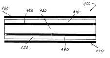
- FIG. 4shows a second exemplary embodiment of a thin laminate film structure 400 .
- the thin laminate film structure 400comprises a first dielectric lamina 410 , a first metallic lamina 420 , a third lamina 430 , a second metallic lamina 440 , and a second dielectric lamina 450 .
- the laminae 410 - 450are attached or bonded together, for example, by a thin film adhesive between respective layers.
- the first metallic lamina 420is attached to or formed on a surface of the first dielectric lamina 410 .
- the first dielectric lamina 410 and the first metallic lamina 420may comprise an aluminized mylar sheet.
- the third lamina 430is attached or bonded to a surface of the first metallic lamina 420 opposite the first dielectric lamina 410 .
- the third lamina 430may comprise a mylar sheet.
- the second metallic lamina 440is similarly attached to or formed on a surface of the second dielectric lamina 450 with the third lamina 430 attached or bonded to a surface of the second metallic lamina 440 opposite the second dielectric lamina 450 .
- the second dielectric lamina 450 and the second metallic lamina 440also may comprise an aluminized mylar sheet.
- the thin laminate film structure 400allows dual-direction actuation of electrostatically and/or magnetically driven devices in which the thin laminate film structure 400 is employed.
- a first electrode 460 and a second electrode 470may be included in such a device for driving the thin laminate film structure 400 in opposite directions.
- the mechanical and electrical/magnetic properties of the thin laminate film structure 400may be optimized separately and/or independently by design of the first and second dielectric laminae 410 and 450 and the third lamina 330 , respectively. Further, the electrical and/or magnetic properties of the thin laminate film structure 400 with respect each dielectric lamina 410 , 450 may be substantially independent by using a dielectric material for the third lamina 430 .
- the first and second dielectric laminae 410 and 450are each thick enough to insulate the first and second metallic laminae 420 and 440 from electrical contact with the first and second electrodes 460 and 470 , respectively.
- the first and second dielectric laminae 410 and 450may be made thinner and may be determined without adversely affecting the mechanical properties of the thin laminate film structure 400 .
- the third lamina 430is thick enough to provide a desired stiffness and/or strength to the thin laminate film structure 400 for a given application. Since the third lamina 430 may be made of a non-dielectric material and/or may be formed on surfaces of the first and second metallic lamina 420 and 440 opposite the first and second dielectric lamina 410 and 450 , respectively, the thickness of the third lamina 430 will not adversely affect the electrical and/or magnetic properties of the thin laminate film structure 400 .
- the thin laminate film structures of this inventionmay be used in a wide variety of other electrostatic or magnetic applications.
- an electrostatically or magnetically actuated film structuremay be used for optical light path deflection.
- an externally applied forcecan be sensed from a measured change in capacitance, which may be used in applications such as, for example, keypads.
- the film stiffnesscan be selected to match the applied forces to optimize membrane deflections.
Landscapes
- Engineering & Computer Science (AREA)
- General Engineering & Computer Science (AREA)
- Mechanical Engineering (AREA)
- Dispersion Chemistry (AREA)
- Chemical & Material Sciences (AREA)
- Theoretical Computer Science (AREA)
- Physics & Mathematics (AREA)
- Fluid Mechanics (AREA)
- Microelectronics & Electronic Packaging (AREA)
- Computer Hardware Design (AREA)
- Laminated Bodies (AREA)
- Electrically Driven Valve-Operating Means (AREA)
- Micromachines (AREA)
Abstract
Description
Claims (20)
Priority Applications (2)
| Application Number | Priority Date | Filing Date | Title |
|---|---|---|---|
| US09/749,431US6676106B2 (en) | 2000-12-28 | 2000-12-28 | Flap structure for electrostatic or magnetic applications and method for making same |
| JP2001388694AJP2002225183A (en) | 2000-12-28 | 2001-12-21 | Membrane laminated film structure for electrostatic or magnetic application apparatus and method for manufacturing the same |
Applications Claiming Priority (1)
| Application Number | Priority Date | Filing Date | Title |
|---|---|---|---|
| US09/749,431US6676106B2 (en) | 2000-12-28 | 2000-12-28 | Flap structure for electrostatic or magnetic applications and method for making same |
Publications (2)
| Publication Number | Publication Date |
|---|---|
| US20020086149A1 US20020086149A1 (en) | 2002-07-04 |
| US6676106B2true US6676106B2 (en) | 2004-01-13 |
Family
ID=25013734
Family Applications (1)
| Application Number | Title | Priority Date | Filing Date |
|---|---|---|---|
| US09/749,431Expired - Fee RelatedUS6676106B2 (en) | 2000-12-28 | 2000-12-28 | Flap structure for electrostatic or magnetic applications and method for making same |
Country Status (2)
| Country | Link |
|---|---|
| US (1) | US6676106B2 (en) |
| JP (1) | JP2002225183A (en) |
Cited By (6)
| Publication number | Priority date | Publication date | Assignee | Title |
|---|---|---|---|---|
| US20040065858A1 (en)* | 2002-10-07 | 2004-04-08 | Thaddeus Schroeder | Unibody valve and techniques for making same for a purge control device |
| US20060135939A1 (en)* | 2004-12-17 | 2006-06-22 | Houston Brown | Electret enhanced automatic IV drip chamber shutoff |
| US20090217997A1 (en)* | 2005-05-04 | 2009-09-03 | Alan Feinerman | Thin welded sheets fluid pathway |
| US20140209824A1 (en)* | 2007-06-20 | 2014-07-31 | So Elektronik Ab | Electromechanical Valve |
| US20150298444A1 (en)* | 2013-10-15 | 2015-10-22 | Shenzhen China Star Optoelectronics Technology Co., Ltd. | Vacuum Suction Adjustable Transfer Roller And Film Attachment Method Using the Transfer Roller |
| EP4384734A4 (en)* | 2021-08-09 | 2025-06-18 | Sartorius Stedim FMT | Actuated elastic valves |
Families Citing this family (5)
| Publication number | Priority date | Publication date | Assignee | Title |
|---|---|---|---|---|
| US6786708B2 (en)* | 2002-07-18 | 2004-09-07 | The Regents Of The University Of Michigan | Laminated devices and methods of making same |
| US7100453B2 (en)* | 2003-12-30 | 2006-09-05 | Honeywell International Inc. | Modified dual diaphragm pressure sensor |
| US6901807B1 (en)* | 2003-12-30 | 2005-06-07 | Honeywell International Inc. | Positive and negative pressure sensor |
| MY155726A (en)* | 2011-11-01 | 2015-11-17 | Mimos Berhad | A microfluidic system and method thereof |
| GB201907171D0 (en)* | 2019-05-21 | 2019-07-03 | Thermo Fisher Scient Bremen Gmbh | Switchable ion guide |
Citations (9)
| Publication number | Priority date | Publication date | Assignee | Title |
|---|---|---|---|---|
| US3118785A (en)* | 1961-10-30 | 1964-01-21 | Gen Electric | Recording film having a thermoplastic polyester image receiving layer |
| US3170833A (en)* | 1961-03-02 | 1965-02-23 | Du Pont | Adhesive compositions and laminates prepared therefrom |
| US3308004A (en)* | 1937-05-10 | 1967-03-07 | Rhone Poulenc Sa | Translucent panels having selective transmission and their manufacture |
| US4543295A (en)* | 1980-09-22 | 1985-09-24 | The United States Of America As Represented By The Director Of The National Aeronautics And Space Administration | High temperature polyimide film laminates and process for preparation thereof |
| US4934401A (en)* | 1988-11-17 | 1990-06-19 | Smc Corporation | Nozzle flapper mechanism |
| US5082242A (en)* | 1989-12-27 | 1992-01-21 | Ulrich Bonne | Electronic microvalve apparatus and fabrication |
| US5441597A (en)* | 1992-12-01 | 1995-08-15 | Honeywell Inc. | Microstructure gas valve control forming method |
| US6032923A (en) | 1998-01-08 | 2000-03-07 | Xerox Corporation | Fluid valves having cantilevered blocking films |
| US6123316A (en) | 1996-11-27 | 2000-09-26 | Xerox Corporation | Conduit system for a valve array |
- 2000
- 2000-12-28USUS09/749,431patent/US6676106B2/ennot_activeExpired - Fee Related
- 2001
- 2001-12-21JPJP2001388694Apatent/JP2002225183A/enactivePending
Patent Citations (10)
| Publication number | Priority date | Publication date | Assignee | Title |
|---|---|---|---|---|
| US3308004A (en)* | 1937-05-10 | 1967-03-07 | Rhone Poulenc Sa | Translucent panels having selective transmission and their manufacture |
| US3170833A (en)* | 1961-03-02 | 1965-02-23 | Du Pont | Adhesive compositions and laminates prepared therefrom |
| US3118785A (en)* | 1961-10-30 | 1964-01-21 | Gen Electric | Recording film having a thermoplastic polyester image receiving layer |
| US4543295A (en)* | 1980-09-22 | 1985-09-24 | The United States Of America As Represented By The Director Of The National Aeronautics And Space Administration | High temperature polyimide film laminates and process for preparation thereof |
| US4934401A (en)* | 1988-11-17 | 1990-06-19 | Smc Corporation | Nozzle flapper mechanism |
| US5082242A (en)* | 1989-12-27 | 1992-01-21 | Ulrich Bonne | Electronic microvalve apparatus and fabrication |
| US5441597A (en)* | 1992-12-01 | 1995-08-15 | Honeywell Inc. | Microstructure gas valve control forming method |
| US6123316A (en) | 1996-11-27 | 2000-09-26 | Xerox Corporation | Conduit system for a valve array |
| US6032923A (en) | 1998-01-08 | 2000-03-07 | Xerox Corporation | Fluid valves having cantilevered blocking films |
| US6120002A (en)* | 1998-01-08 | 2000-09-19 | Xerox Corporation | Fluid valves having cantilevered blocking films |
Non-Patent Citations (2)
| Title |
|---|
| Biegelsen, et al., AirJet paper mover: An example of meso-scale MEMS. |
| D. Biegelsen, et al., "High performance electrostatic air valves formed by thin-film lamination," Proceedings of the Symposium on Micro-Mechanical Systems, ASME International Mechanical Engineering Congress and Exhibition, Nashville, TN, published 1999. |
Cited By (10)
| Publication number | Priority date | Publication date | Assignee | Title |
|---|---|---|---|---|
| US20040065858A1 (en)* | 2002-10-07 | 2004-04-08 | Thaddeus Schroeder | Unibody valve and techniques for making same for a purge control device |
| US6786468B2 (en)* | 2002-10-07 | 2004-09-07 | Delphi Technologies, Inc. | Unibody valve and techniques for making same for a purge control device |
| US20060135939A1 (en)* | 2004-12-17 | 2006-06-22 | Houston Brown | Electret enhanced automatic IV drip chamber shutoff |
| US7338475B2 (en)* | 2004-12-17 | 2008-03-04 | Cardinal Health 303, Inc. | Electret enhanced automatic IV drip chamber shutoff |
| US20090217997A1 (en)* | 2005-05-04 | 2009-09-03 | Alan Feinerman | Thin welded sheets fluid pathway |
| US20140209824A1 (en)* | 2007-06-20 | 2014-07-31 | So Elektronik Ab | Electromechanical Valve |
| US9157546B2 (en)* | 2007-06-20 | 2015-10-13 | So Elektronik Ab | Electromechanical valve |
| US20150298444A1 (en)* | 2013-10-15 | 2015-10-22 | Shenzhen China Star Optoelectronics Technology Co., Ltd. | Vacuum Suction Adjustable Transfer Roller And Film Attachment Method Using the Transfer Roller |
| US9370919B2 (en)* | 2013-10-15 | 2016-06-21 | Shenzhen China Star Optoelectronics Technology Co., Ltd | Vacuum suction adjustable transfer roller and film attachment method using the transfer roller |
| EP4384734A4 (en)* | 2021-08-09 | 2025-06-18 | Sartorius Stedim FMT | Actuated elastic valves |
Also Published As
| Publication number | Publication date |
|---|---|
| JP2002225183A (en) | 2002-08-14 |
| US20020086149A1 (en) | 2002-07-04 |
Similar Documents
| Publication | Publication Date | Title |
|---|---|---|
| US6676106B2 (en) | Flap structure for electrostatic or magnetic applications and method for making same | |
| EP0544405B1 (en) | Piezoelectric fluid flow control valve | |
| US5909078A (en) | Thermal arched beam microelectromechanical actuators | |
| US11724932B2 (en) | Integrated micro-electromechanical device of semiconductor material having a diaphragm | |
| US5029805A (en) | Valve arrangement of microstructured components | |
| JP4205202B2 (en) | Magnetic microswitch and manufacturing method thereof | |
| Hosaka et al. | Electromagnetic microrelays: concepts and fundamental characteristics | |
| US5593134A (en) | Magnetically assisted piezo-electric valve actuator | |
| JP3147938B2 (en) | Liquid outflow control valve, microvalve, and method of controlling liquid outflow control valve | |
| US5065978A (en) | Valve arrangement of microstructured components | |
| US8669627B2 (en) | MEMS element and method for manufacturing same | |
| US6715731B1 (en) | Piezoelectric valve | |
| US8604670B2 (en) | Piezoelectric ALN RF MEM switches monolithically integrated with ALN contour-mode resonators | |
| US20050018322A1 (en) | Magnetically actuated fast MEMS mirrors and microscanners | |
| JPH04282085A (en) | Micro valve of multilayered structure | |
| KR20070090843A (en) | Flow control device | |
| JP2009507655A (en) | Manufacturing method of micro system, micro system, laminated body of foil having macro system, electronic device having micro system, and use of electronic device | |
| EP0218430B1 (en) | Magnetic actuator | |
| US20060082427A1 (en) | Method and apparatus for reducing cantilever stress in magnetically actuated relays | |
| JP2002010612A (en) | Electromagnetic actuator, method of manufacturing the electromagnetic actuator, and optical deflector using the electromagnetic actuator | |
| US5093600A (en) | Piezo-electric relay | |
| Sakata et al. | Pb-based ferroelectric thin film actuator for optical applications | |
| US7422191B2 (en) | Bistable miniature valve | |
| Quandt et al. | Giant magnetostrictive multilayers for thin film actuators | |
| Ikehara et al. | Electromagnetically driven silicon microvalve for large-flow pneumatic controls |
Legal Events
| Date | Code | Title | Description |
|---|---|---|---|
| AS | Assignment | Owner name:XEROX CORPORATION, CONNECTICUT Free format text:ASSIGNMENT OF ASSIGNORS INTEREST;ASSIGNORS:SWARTZ, LARS. E.;BIEGELSEN, DAVID K.;REEL/FRAME:011773/0227 Effective date:20010328 | |
| AS | Assignment | Owner name:BANK ONE, NA, AS ADMINISTRATIVE AGENT, ILLINOIS Free format text:SECURITY AGREEMENT;ASSIGNOR:XEROX CORPORATION;REEL/FRAME:013111/0001 Effective date:20020621 Owner name:BANK ONE, NA, AS ADMINISTRATIVE AGENT,ILLINOIS Free format text:SECURITY AGREEMENT;ASSIGNOR:XEROX CORPORATION;REEL/FRAME:013111/0001 Effective date:20020621 | |
| AS | Assignment | Owner name:JPMORGAN CHASE BANK, AS COLLATERAL AGENT, TEXAS Free format text:SECURITY AGREEMENT;ASSIGNOR:XEROX CORPORATION;REEL/FRAME:015134/0476 Effective date:20030625 Owner name:JPMORGAN CHASE BANK, AS COLLATERAL AGENT,TEXAS Free format text:SECURITY AGREEMENT;ASSIGNOR:XEROX CORPORATION;REEL/FRAME:015134/0476 Effective date:20030625 | |
| FEPP | Fee payment procedure | Free format text:PAYOR NUMBER ASSIGNED (ORIGINAL EVENT CODE: ASPN); ENTITY STATUS OF PATENT OWNER: LARGE ENTITY | |
| CC | Certificate of correction | ||
| AS | Assignment | Owner name:JPMORGAN CHASE BANK, AS COLLATERAL AGENT, TEXAS Free format text:SECURITY AGREEMENT;ASSIGNOR:XEROX CORPORATION;REEL/FRAME:015722/0119 Effective date:20030625 Owner name:JPMORGAN CHASE BANK, AS COLLATERAL AGENT,TEXAS Free format text:SECURITY AGREEMENT;ASSIGNOR:XEROX CORPORATION;REEL/FRAME:015722/0119 Effective date:20030625 | |
| FPAY | Fee payment | Year of fee payment:4 | |
| CC | Certificate of correction | ||
| FPAY | Fee payment | Year of fee payment:8 | |
| REMI | Maintenance fee reminder mailed | ||
| LAPS | Lapse for failure to pay maintenance fees | ||
| STCH | Information on status: patent discontinuation | Free format text:PATENT EXPIRED DUE TO NONPAYMENT OF MAINTENANCE FEES UNDER 37 CFR 1.362 | |
| FP | Lapsed due to failure to pay maintenance fee | Effective date:20160113 | |
| AS | Assignment | Owner name:XEROX CORPORATION, CONNECTICUT Free format text:RELEASE BY SECURED PARTY;ASSIGNOR:JPMORGAN CHASE BANK, N.A. AS SUCCESSOR-IN-INTEREST ADMINISTRATIVE AGENT AND COLLATERAL AGENT TO BANK ONE, N.A.;REEL/FRAME:061360/0501 Effective date:20220822 | |
| AS | Assignment | Owner name:XEROX CORPORATION, CONNECTICUT Free format text:RELEASE BY SECURED PARTY;ASSIGNOR:JPMORGAN CHASE BANK, N.A. AS SUCCESSOR-IN-INTEREST ADMINISTRATIVE AGENT AND COLLATERAL AGENT TO BANK ONE, N.A.;REEL/FRAME:061388/0388 Effective date:20220822 Owner name:XEROX CORPORATION, CONNECTICUT Free format text:RELEASE BY SECURED PARTY;ASSIGNOR:JPMORGAN CHASE BANK, N.A. AS SUCCESSOR-IN-INTEREST ADMINISTRATIVE AGENT AND COLLATERAL AGENT TO JPMORGAN CHASE BANK;REEL/FRAME:066728/0193 Effective date:20220822 |