US6674134B2 - Structure and method for dual gate oxidation for CMOS technology - Google Patents
Structure and method for dual gate oxidation for CMOS technologyDownload PDFInfo
- Publication number
- US6674134B2 US6674134B2US09/173,430US17343098AUS6674134B2US 6674134 B2US6674134 B2US 6674134B2US 17343098 AUS17343098 AUS 17343098AUS 6674134 B2US6674134 B2US 6674134B2
- Authority
- US
- United States
- Prior art keywords
- regions
- integrated circuit
- oxide
- device regions
- preselected
- Prior art date
- Legal status (The legal status is an assumption and is not a legal conclusion. Google has not performed a legal analysis and makes no representation as to the accuracy of the status listed.)
- Expired - Fee Related, expires
Links
Images


Classifications
- H—ELECTRICITY
- H01—ELECTRIC ELEMENTS
- H01L—SEMICONDUCTOR DEVICES NOT COVERED BY CLASS H10
- H01L21/00—Processes or apparatus adapted for the manufacture or treatment of semiconductor or solid state devices or of parts thereof
- H01L21/70—Manufacture or treatment of devices consisting of a plurality of solid state components formed in or on a common substrate or of parts thereof; Manufacture of integrated circuit devices or of parts thereof
- H01L21/77—Manufacture or treatment of devices consisting of a plurality of solid state components or integrated circuits formed in, or on, a common substrate
- H—ELECTRICITY
- H01—ELECTRIC ELEMENTS
- H01L—SEMICONDUCTOR DEVICES NOT COVERED BY CLASS H10
- H01L21/00—Processes or apparatus adapted for the manufacture or treatment of semiconductor or solid state devices or of parts thereof
- H01L21/70—Manufacture or treatment of devices consisting of a plurality of solid state components formed in or on a common substrate or of parts thereof; Manufacture of integrated circuit devices or of parts thereof
- H01L21/71—Manufacture of specific parts of devices defined in group H01L21/70
- H01L21/76—Making of isolation regions between components
- H01L21/762—Dielectric regions, e.g. EPIC dielectric isolation, LOCOS; Trench refilling techniques, SOI technology, use of channel stoppers
- H01L21/76224—Dielectric regions, e.g. EPIC dielectric isolation, LOCOS; Trench refilling techniques, SOI technology, use of channel stoppers using trench refilling with dielectric materials
- H—ELECTRICITY
- H10—SEMICONDUCTOR DEVICES; ELECTRIC SOLID-STATE DEVICES NOT OTHERWISE PROVIDED FOR
- H10D—INORGANIC ELECTRIC SEMICONDUCTOR DEVICES
- H10D84/00—Integrated devices formed in or on semiconductor substrates that comprise only semiconducting layers, e.g. on Si wafers or on GaAs-on-Si wafers
- H10D84/01—Manufacture or treatment
- H10D84/0123—Integrating together multiple components covered by H10D12/00 or H10D30/00, e.g. integrating multiple IGBTs
- H10D84/0126—Integrating together multiple components covered by H10D12/00 or H10D30/00, e.g. integrating multiple IGBTs the components including insulated gates, e.g. IGFETs
- H10D84/0144—Manufacturing their gate insulating layers
- H—ELECTRICITY
- H10—SEMICONDUCTOR DEVICES; ELECTRIC SOLID-STATE DEVICES NOT OTHERWISE PROVIDED FOR
- H10D—INORGANIC ELECTRIC SEMICONDUCTOR DEVICES
- H10D84/00—Integrated devices formed in or on semiconductor substrates that comprise only semiconducting layers, e.g. on Si wafers or on GaAs-on-Si wafers
- H10D84/01—Manufacture or treatment
- H10D84/0123—Integrating together multiple components covered by H10D12/00 or H10D30/00, e.g. integrating multiple IGBTs
- H10D84/0126—Integrating together multiple components covered by H10D12/00 or H10D30/00, e.g. integrating multiple IGBTs the components including insulated gates, e.g. IGFETs
- H10D84/0151—Manufacturing their isolation regions
- H—ELECTRICITY
- H10—SEMICONDUCTOR DEVICES; ELECTRIC SOLID-STATE DEVICES NOT OTHERWISE PROVIDED FOR
- H10D—INORGANIC ELECTRIC SEMICONDUCTOR DEVICES
- H10D84/00—Integrated devices formed in or on semiconductor substrates that comprise only semiconducting layers, e.g. on Si wafers or on GaAs-on-Si wafers
- H10D84/01—Manufacture or treatment
- H10D84/02—Manufacture or treatment characterised by using material-based technologies
- H10D84/03—Manufacture or treatment characterised by using material-based technologies using Group IV technology, e.g. silicon technology or silicon-carbide [SiC] technology
- H10D84/038—Manufacture or treatment characterised by using material-based technologies using Group IV technology, e.g. silicon technology or silicon-carbide [SiC] technology using silicon technology, e.g. SiGe
Definitions
- the present inventionrelates to a semiconductor integrated circuit, and in particular to a dynamic access memory (DRAM) metal oxide semiconductor field effect transistor (MOSFET) which contains gate oxide regions having various oxide thicknesses that are dependent upon the width of the active device areas.
- DRAMdynamic access memory
- MOSFETmetal oxide semiconductor field effect transistor
- the present inventionalso provides an improved gate oxidation process useful in fabricating such a DRAM MOSFET structure wherein the gate oxide thickness is determined by the channel width of the MOSFET structure.
- the threshold voltage of the devicedoes not scale with the power supply voltage and ground rules because of the non-scalability of the sub-threshold slope.
- the minimum gate oxide thickness and/or maximum wordline boost voltage of the array MOSFETis constrained by reliability considerations.
- the relatively thick gate oxide(having a thickness of greater than ⁇ 6 nm for 0.175 ⁇ m technology) required by the array MOSFET results in degradation in the performance of the MOSFET device. Furthermore, if a thinner gate oxide is used to improve the performance of the support circuitry, charge transfer efficiency in the device array is compromised as a result of the reliability limitation of the wordline boost voltage.
- a dual gate oxide thicknessis desired.
- additional gate oxidation processing stepsare costly, and they are also yield limiting since one must utilize additional processing steps such as but not limited to: masking, exposure, etching, oxidizing and strip masking, which either grow a second oxide or mask an existing oxide introducing defect sources into the entire structure of the MOSFET device.
- additional processing stepssuch as but not limited to: masking, exposure, etching, oxidizing and strip masking, which either grow a second oxide or mask an existing oxide introducing defect sources into the entire structure of the MOSFET device.
- prior art gate oxidation processesare not reliable nor cost efficient.
- One object of the present inventionis to provide a dual gate oxidation process for use in DRAM technologies having feature sizes of about 0.15 ⁇ m or less which does not impose the additional manufacturing steps or costs required by prior gate oxidation processes.
- Another object of the present inventionis to provide a dual gate oxidation process which provides a path for growing a thicker gate oxide on the DRAM transistor relative to the support transistor allowing for increased gate voltage, reduced vertical electrical field and improved corner reliability to electric field.
- a still further object of the present inventionis to design a DRAM MOSFET having a minimum ground rule width, to maximize density.
- An additional object of the present inventionis to provide thicker gate oxide MOSFETs having high current capability suitable for reliable I/O devices capable of interfacing with circuitry external to a semiconductor chip operating at voltages which are higher than on the chip.
- the thickness of the gate oxideis determined, i.e. controlled, by the width of the channel the MOSFET; narrow width devices having a gate oxide thickness which is greater than those for wide devices.
- the differential in gate oxide thicknessmay be enhanced in the present invention by decreasing the radius of curvature (increasing sharpness) of the silicon corners.
- One aspect of the present inventionrelates to an integrated circuit, i.e. DRAM MOSFET, which comprises a semiconductor substrate having a plurality of device regions formed therein, said plurality of device regions being electrically isolated from each other by shallow trench isolation (STI) regions, said plurality of device regions each having opposing edges abutting its corresponding STI region;
- STIshallow trench isolation
- this objectis met by providing a plurality of parallel arrayed nested mesa MOSFETs having a narrow width, wherein each narrow MOSFET has a gate oxide which is thicker than the gate oxide of MOSFETs having a mesa with a wider width.
- Another aspect of the present inventionrelates to a dual gate oxidation process which can be used in fabricating the above described integrated circuit.
- the dual gate oxidation process of the present inventioncomprises the steps of:
- the conditions employed during the gate oxidation stepare carefully selected so as to allow flow of the oxide material away from the corners of the device regions.
- This stepallows one to obtain the above structure wherein a thicker gate oxide is grown on a narrower portion of the device structure and a thinner gate oxide is grown on the wider portions of the device structure.
- Such dual oxide gate thicknessescannot be obtained by prior art processes utilizing a single gate oxidation step.
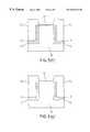
- FIG. 1is a cross-sectional view showing an integrated circuit that can be manufactured using the method of the present invention.
- FIG. 2is a cross-sectional view showing an alternative integrated circuit having a high degree of curvature that can be manufactured using the method of the present invention.
- FIGS. 3 ( a )-( g )are cross-sectional view of the structure of FIG. 1 after various processing steps of the present invention.
- FIG. 4is a cross-sectional view of a plurality of nested narrow mesa devices in parallel arrangement.
- FIGS. 5 ( a )-( b )are TEM photographs of: (a) 198 nm wide device having a 8 nm gate oxide region; and (b) a 53 nm narrow device having a 12 nm gate oxide region.
- the present inventionwhich provides a dual gate DRAM MOSFET structure having different gate oxide thicknesses that are determined by the width of the active device regions, will now be described in greater detail with reference to the accompanying drawings wherein like elements or components are referred to by like and corresponding reference numerals.
- FIGS. 1 and 2are cross-sectional views illustrating integrated circuits (ICs) that can be manufactured using the process of the present invention.
- ICsintegrated circuits
- FIG. 1the active device regions have perfectly sharp 90° corners having little or no radius of curvature.
- the structure shown in FIG. 2has a radius of curvature which is greater than 0 nm.
- the radius of curvature of the corners of the active device regionsis from about 1 to about 30 nm.
- FIGS. 1 and 2comprise a semiconductor substrate or wafer 10 having a plurality of active device regions 12 formed in semiconductor substrate 10 (only two of which are illustrated in the drawings).
- the active device regions 12are isolated from each other by shallow trench isolation regions (STI) 14 which are also formed in semiconductor substrate 10 and have opposing edges which abut its corresponding STI region.
- STIshallow trench isolation regions
- Each active device regioncomprises source/drain regions which are located perpendicular to the plane of the paper; therefore the source/drain regions are not depicted in the drawings of the present application.
- the active device regions in FIG. 1have perfectly sharp 90° corners while the active device regions in FIG. 2 have a high degree of curvature associated therewith.
- the integrated circuit shown in FIG. 1 or 2comprises a first device region 12 a which has a preselected first device width, d 1 , such that an oxide layer 16 formed thereon, i.e. gate oxide, includes substantially thicker perimeter regions 16 a , along opposing edges, compared to a thinner central region 16 b that does not abut the corresponding STI region.
- d 1first device width
- the structures shown in FIGS. 1 and 2also include another device region 12 b having a predetermined device width, d 2 , which is substantially narrower than the device width of device region 12 a (d 1 ) such that an oxide layer 16 formed thereon includes perimeter regions 16 a , along opposing edges, that abut each other over a central region 16 b thereby preventing formation of a thinner central region.
- the narrower device widthhas a thicker oxide region 16 formed thereon as compared to the thinner oxide region 16 which is achieved over the wide device region.
- the wide active device regionhas a width, d 1 , that is from about 0.18 to about 20 ⁇ m whereas the narrow device region, d 2 , has a width of from about 0.03 to about 0.15 ⁇ m. More preferably, d 1 is from about 5 to about 20 ⁇ m whereas d 2 is from about 0.06 to about 0.12 ⁇ m.
- the above rangescorrelate to a gate oxide that has a thickness of from about 2.5 to about 9.0 nm for d 1 and from about 5.0 to about 14.0 nm for d 2 . More preferably, the preferred ranges correlate to a gate oxide thickness for d 1 that is from about 3.0 to about 4.0 nm and a gate oxide thickness for d 2 that is from about 5.5 to about 6.5 nm.
- the integrated circuits shown in FIGS. 1 and 2also contain an oxygen barrier, i.e. nitride liner, 18 which is positioned in STI region 14 .
- the oxygen barrier layeris composed of a conventional barrier layer material such as Si 3 N 4 that is capable of preventing oxygen from diffusing to the semiconductor substrate or wafer.
- oxygen barrier layer 18is optional in the present invention.
- structures not containing oxygen barrier layer 18are also within the contemplation of the present invention. While representing an optional embodiment of the present invention, it is noted that the presence of oxygen barrier layer 18 near the active device corners alters the stress pattern such that any oxide grown at the corners is pushed towards the middle of the device mesa.
- Oxide growing between oxygen barrier layer 18 and device regions 12 a and 12 bis squeezed by the compressive stress generated in that region. This compressive stress forces the flowable oxide away from the corner. Since oxygen barrier layer 18 is relatively rigid compared to the flowable oxygen it resists deformation. This results in a reactive force which pushes the growing oxide away. The higher the top of the oxygen barrier layer relative to the top of the mesa, the more effective this push. Thus it is important in the present invention to control the etch which removes polish stop layer 19 since this etch also attacks and recesses oxygen barrier layer 18 . Overetching should be avoided.
- the present inventionis also applicable for forming I/O devices which are capable of interfacing with circuitry external to the semiconductor wafer.
- the present inventioncan be used to provide thicker gate oxides MOSFETs having high current drive capabilities. This is achieved in the present invention by providing the structure shown in FIG. 4 .
- the structure of FIG. 4comprises a plurality of nested narrow mesa devices which are arranged in parallel.
- the structurecomprises semiconductor substrate or wafer 10 having a plurality of active device regions 12 which are in parallel arrangement and are spaced apart by STI regions 14 .
- the active device regionshave a narrow mesa width, d 2 , associated therewith.
- a partial segment of an active device region having a wider mesa, d 1is also shown. It is noted that wider mesa, d 1 , has a thinner oxide region as compared to the oxide region over d 2 .
- the structuresare designed by taking into account the minimum ground rule width to exploit the oxide thickness dependence on width. This results in the device being manufactured in a small semiconductor mesa as compared with prior art processes wherein device manufacturing is typically carried out on larger semiconductor mesas.
- FIGS. 5 ( a )-( b )are TEM photographs for a device containing a 198 nm wide device region (See FIG. 5 ( a )) and a device containing a 53 nm wide device region (See FIG. 5 ( b )). It is noted that for the device shown in FIG. 5 ( a ) the active device region has a gate oxide of about 8 nm formed thereon whereas in FIG. 5 ( b ) the gate oxide over the narrower device region has a thickness of about 12 nm. This demonstrates the basic concept of the present invention that narrower device regions contain a thicker gate oxide as compared to wider device regions which contain thinner gate oxide regions.
- FIGS. 3 ( a )-( g )show the various processing steps utilized in the present invention in manufacturing the structures shown in FIGS. 1, 2 , 4 and 5 ( a )-( b ) in greater detail with reference to FIGS. 3 ( a )-( g ). Attention is first made to FIG. 3 ( a ) which shows the initial structure that is employed in the present invention. It should be emphasized that although these figures contain device regions having sharp 90° corners, the present processing steps are also applicable for producing the structure shown in FIG. 2, i.e. they can be used in manufacturing a structure which contains a high degree of curvature.
- the initial structure shown in FIG. 3 ( a )comprises a semiconductor substrate or wafer 10 which has a thin oxide pad 20 formed on its surface and a polish stop layer 19 (i.e. Si 3 N 4 ) positioned atop of oxide pad 20 .
- a polish stop layer 19i.e. Si 3 N 4
- the polish stop layeris also referred to in the art as a pad layer.
- the semiconductor substrate or wafer 10is composed of any semiconducting material including, but not limited to: Si, Ge, SiGe, GaAs, InAs, InP and all other III/V compounds. Of these semiconductor materials, it is highly preferred that semiconductor substrate or wafer 10 be composed of silicon.
- the semiconductor substrate or wafermay be of the p-type or the n-type depending on the type of integrated circuit being manufactured.
- Oxide pad 20is composed of any oxide material such as SiO 2 which is capable of being grown thermally or deposited by conventional techniques well known to those skilled in the art.
- the thickness of the oxide pad layer while not being critical to the present inventionis however in the range of from about 3 to about 10 nm. More preferably, oxide pad 20 has a thickness of from about 5 to about 8 nm.
- the polish stop layeris composed of any conventional relatively hard material, e.g. Si 3 N 4 , which is capable of slowing the polishing process and it is formed on top of oxide pad 20 utilizing standard deposition techniques and conditions well known to those skilled in the art.
- chemical vapor deposition, plasma enhanced chemical vapor deposition, plasma vapor deposition, sputtering and other like deposition techniquescan be employed in the present invention in forming polish stop layer 19 .
- the thickness of the polish stop layermay vary depending upon the etching and planarization processes employed in the present invention. Typically, however, the thickness of the polish stop layer is from about 50 to about 350 nm. More preferably, the thickness of the layer is from about 100 to about 200 nm.
- active device regions 12which will contain the MOSFET are predetermined and are formed in the present invention utilizing conventional techniques well known to those skilled in the art.
- FIG. 3 ( b )illustrates the employment of a photoresist 22 which is patterned on the surface of polish stop layer or pad 19 .
- shallow trenchesare formed into semiconductor substrate or wafer 10 utilizing standard etching techniques well known to those skilled in the art. Any anisotropic dry etching technique can be employed in the present invention. Thus, etching may be performed by reactive ion etching, plasma etching and ion beam etching.
- etchingis performed to any predetermined depth into the semiconductor substrate or wafer. Typically, depth ranges are from about 0.08 to about 0.6 ⁇ m. More preferably, the trenches are etched to a depth of from about 0.15 to about 0.30 ⁇ m.
- the shallow trench etching stepis illustrated in FIG. 3 ( c ).
- a thermal oxide 26e.g. SiO 2 is grown to line the surface of the shallow trenches utilizing conventional oxidation techniques well known to those skilled in the art.
- the thermal oxide lineris grown to a thickness that is from about 3 to about 30 nm. More preferably, the thermal oxide has a thickness of from about 5 to about 20 nm.
- an optional oxygen barrier layer 18can be formed on the surface of thermal oxide 26 utilizing the deposition techniques mentioned hereinabove.
- the thickness of the optional oxygen barrier layeris typically of from about 3 to about 20 nm. More preferably, the optional oxygen barrier layer has a thickness of from about 4 to about 10 nm. The above two steps of the process of the present invention are shown in FIG. 3 ( d ).
- a chemical vapor deposited oxide 28such as tetraethylorthosilicate (TEOS) is formed on the top surface of the structure and the structure is then planarized stopping at polish stop layer 19 using conventional planarization techniques such as chemical mechanical polishing (CMP) or grinding.
- CMPchemical mechanical polishing
- the remaining pad layers, i.e. polish stop layer, and oxide pad not covered by the CVD oxide and located over the active device regionsare then removed using a chemical etchant such as but not limited to: hot phosphoric acid, followed by buffered HF.
- a chemical etchantsuch as but not limited to: hot phosphoric acid, followed by buffered HF.
- a sacrificial oxide 29is formed on the exposed surface of the semiconductor substrate under conditions to produce a predetermined radius of curvature in the semiconductor wafer (See, FIG. 3 ( f )).
- Thismay be carrier out in the present invention by a thermal oxidation step, a step of depositing a sacrificial oxide followed by selective etching or a combination of thermal oxidation and etching.
- thermal growingis carried out using a rapid thermal oxidation process in dry O 2 at 1050° C. for 35 seconds.
- an oxide layerwhen first deposited, it can be deposited by a selective deposition process well known to those skilled in the art and then etched to provide a predetermined radius of curvature to the structure.
- Suitable selective etching processesthat can be employed in this step of the present invention include: reactive ion etching, plasma etching, ion beam etching, wet and chemical dry etching.
- N-well and N-well doping regionsare formed in the surface of the semiconductor substrate utilizing conventional ion implantation techniques and conditions well known by those skilled in the art.
- N- or p-type dopant atomsmay be implanted into the semiconductor substrate or wafer depending on the type of electronic device being manufactured.
- the sacrificial oxide layeris removed using standard etching techniques which preferably utilize fluorine based chemistries.
- This step of the present inventionwhich does not remove the above obtained radius of curvature introduced into the structure during formation of the sacrificial oxide is shown in FIG. 3 ( g ).
- the next step of the present inventionis a gate oxidation step.
- the gate oxidation stepis conducted under defined conditions so that the thickness of the gate oxide 16 formed is a function of the channel width of the MOSFET.
- the oxidation conditions employed in the present inventionmust be capable of forming an oxide at the corners of the active device regions such that the formed oxide readily flows therefrom.
- oxidization rateis dependent on the silicon corners.
- the geometry of the corneris characterized by the radius of curvature of the silicon.
- Numerical calculations by Kao, et al. suprashow that oxidation rates increase with decreasing radius of curvature at a convex surface being oxidized.
- the supply of oxidantsi.e. dry oxygen, steam plus any other elements introduced to control the electrical and mechanical properties of the oxide
- the oxidation rateis proportional to the supply oxidants.
- the degree of viscosity flowmust be limited in order to establish a gradient in the oxide thickness going away from the corner towards the middle of the mesa. This gradient in oxide thickness is important because it allows the gate oxide thickness to be controlled by the width of the mesa. Therefore, the oxidation conditions employed in the present invention must be selected to produce a desired viscosity.
- the gate oxidation step employed in the present inventionwhich satisfies all of the above mentioned requirements is carried out in an oxidizing ambient at a temperature of greater than 600° C. but lower than 1100° C.
- oxidizing ambientit is meant any oxygen containing ambient including, but not limited to: dry oxygen and steam.
- the gate oxidation stepmay be carried out under high or low pressures with a preferred range being from about 1 mTorr to about 100 atm. A preferred temperature range is from about 800° to about 1000° C.
- the gate oxidation stepis carried out by a furnance oxidation process using dry O 2 . The temperature of the furnance oxidation is ramped up from ambient to 900° C. in N 2 . At this temperature, N 2 is replaced with dry O 2 and heating is carried out for about 9.5 minutes.
- the gate oxidation step of the present inventionmay be carried out for a period of time of from about 20 seconds to about 60 minutes. More preferably, the oxidation step is carried out for a period of time from about 60 seconds to about 15 minutes. It should be noted that shorter oxidation times are typically employed at higher temperatures whereas longer oxidation times are employed for lower oxidation temperatures.
- the present inventiontakes into account the small feature sizes of the MOS device as well as the fact that oxidation conditions should be controlled within defined limits so as to cause substantial flow of the oxide away from the corners of the active device regions.
- Thisallows for the formation of the structures shown in FIGS. 1, 2 , 4 and 5 ( a )-( b ) as well as being able to form gate oxides on the MOSFET device having different thicknesses.
- Such resultscannot be obtained in a single oxidation step utilizing prior art gate oxidation methods. Instead, the prior art requires additional processing steps in order to fabricate the same structure.
- it is essential that the device being manufacturedhas small feature sizes (0.15 ⁇ m and below) and a substantial radius of curvature so as to allow sufficient flow of oxide away from the corners of the active device region during the oxidation step.
Landscapes
- Engineering & Computer Science (AREA)
- Physics & Mathematics (AREA)
- Condensed Matter Physics & Semiconductors (AREA)
- General Physics & Mathematics (AREA)
- Manufacturing & Machinery (AREA)
- Computer Hardware Design (AREA)
- Microelectronics & Electronic Packaging (AREA)
- Power Engineering (AREA)
- Metal-Oxide And Bipolar Metal-Oxide Semiconductor Integrated Circuits (AREA)
- Insulated Gate Type Field-Effect Transistor (AREA)
Abstract
Description
Claims (12)
Priority Applications (3)
| Application Number | Priority Date | Filing Date | Title |
|---|---|---|---|
| US09/173,430US6674134B2 (en) | 1998-10-15 | 1998-10-15 | Structure and method for dual gate oxidation for CMOS technology |
| KR1019990039473AKR100345430B1 (en) | 1998-10-15 | 1999-09-15 | Structure and method for dual gate oxidation for cmos technology |
| US09/421,853US6344383B1 (en) | 1998-10-15 | 1999-10-20 | Structure and method for dual gate oxidation for CMOS technology |
Applications Claiming Priority (1)
| Application Number | Priority Date | Filing Date | Title |
|---|---|---|---|
| US09/173,430US6674134B2 (en) | 1998-10-15 | 1998-10-15 | Structure and method for dual gate oxidation for CMOS technology |
Related Child Applications (1)
| Application Number | Title | Priority Date | Filing Date |
|---|---|---|---|
| US09/421,853DivisionUS6344383B1 (en) | 1998-10-15 | 1999-10-20 | Structure and method for dual gate oxidation for CMOS technology |
Publications (2)
| Publication Number | Publication Date |
|---|---|
| US20010020724A1 US20010020724A1 (en) | 2001-09-13 |
| US6674134B2true US6674134B2 (en) | 2004-01-06 |
Family
ID=22631983
Family Applications (2)
| Application Number | Title | Priority Date | Filing Date |
|---|---|---|---|
| US09/173,430Expired - Fee RelatedUS6674134B2 (en) | 1998-10-15 | 1998-10-15 | Structure and method for dual gate oxidation for CMOS technology |
| US09/421,853Expired - Fee RelatedUS6344383B1 (en) | 1998-10-15 | 1999-10-20 | Structure and method for dual gate oxidation for CMOS technology |
Family Applications After (1)
| Application Number | Title | Priority Date | Filing Date |
|---|---|---|---|
| US09/421,853Expired - Fee RelatedUS6344383B1 (en) | 1998-10-15 | 1999-10-20 | Structure and method for dual gate oxidation for CMOS technology |
Country Status (2)
| Country | Link |
|---|---|
| US (2) | US6674134B2 (en) |
| KR (1) | KR100345430B1 (en) |
Cited By (7)
| Publication number | Priority date | Publication date | Assignee | Title |
|---|---|---|---|---|
| US20010012664A1 (en)* | 1999-09-01 | 2001-08-09 | Tran Luan C. | Semiconductor processing methods of forming transistors, semiconductor processing methods of forming dynamic random access memory circuitry, and related integrated circuitry |
| US20100025770A1 (en)* | 2008-07-31 | 2010-02-04 | Martin Trentzsch | Gate dielectrics of different thickness in pmos and nmos transistors |
| US8437184B1 (en)* | 2011-12-06 | 2013-05-07 | Rexchip Electronics Corporation | Method of controlling a vertical dual-gate dynamic random access memory |
| US20140306323A1 (en)* | 2013-04-10 | 2014-10-16 | Micron Technology, Inc. | Semiconductor Constructions |
| US9576953B2 (en) | 2014-02-03 | 2017-02-21 | Samsung Electronics Co., Ltd. | Layout design system, semiconductor device fabricated by using the system and method for fabricating the semiconductor device |
| US10181426B1 (en)* | 2017-08-30 | 2019-01-15 | Taiwan Semiconductor Manufacturing Co., Ltd. | Etch profile control of polysilicon structures of semiconductor devices |
| US20200044075A1 (en)* | 2017-05-24 | 2020-02-06 | Semiconductor Manufacturing International (Shanghai) Corporation | Semiconductor structure |
Families Citing this family (8)
| Publication number | Priority date | Publication date | Assignee | Title |
|---|---|---|---|---|
| JP4056195B2 (en)* | 2000-03-30 | 2008-03-05 | 株式会社ルネサステクノロジ | Manufacturing method of semiconductor integrated circuit device |
| GB2381383A (en)* | 2000-07-13 | 2003-04-30 | Seagate Technology Llc | Method for topographical patterning of a device |
| US6693041B2 (en)* | 2001-06-20 | 2004-02-17 | International Business Machines Corporation | Self-aligned STI for narrow trenches |
| US6403425B1 (en)* | 2001-11-27 | 2002-06-11 | Chartered Semiconductor Manufacturing Ltd. | Dual gate oxide process with reduced thermal distribution of thin-gate channel implant profiles due to thick-gate oxide |
| US7660327B2 (en)* | 2004-02-03 | 2010-02-09 | Atheros Communications, Inc. | Temporary priority promotion for network communications in which access to a shared medium depends on a priority level |
| KR100577565B1 (en)* | 2004-02-23 | 2006-05-08 | 삼성전자주식회사 | Manufacturing Method of Fin Field Effect Transistor |
| US7326655B2 (en)* | 2005-09-29 | 2008-02-05 | Tokyo Electron Limited | Method of forming an oxide layer |
| KR102443696B1 (en) | 2016-05-31 | 2022-09-15 | 삼성전자주식회사 | method of manufacturing semiconductor device |
Citations (26)
| Publication number | Priority date | Publication date | Assignee | Title |
|---|---|---|---|---|
| US4474624A (en)* | 1982-07-12 | 1984-10-02 | Intel Corporation | Process for forming self-aligned complementary source/drain regions for MOS transistors |
| US4593459A (en)* | 1984-12-28 | 1986-06-10 | Gte Laboratories Incorporated | Monolithic integrated circuit structure and method of fabrication |
| US4633290A (en)* | 1984-12-28 | 1986-12-30 | Gte Laboratories Incorporated | Monolithic CMOS integrated circuit structure with isolation grooves |
| US4651406A (en)* | 1980-02-27 | 1987-03-24 | Hitachi, Ltd. | Forming memory transistors with varying gate oxide thicknesses |
| US4746963A (en)* | 1982-09-06 | 1988-05-24 | Hitachi, Ltd. | Isolation regions formed by locos followed with groove etch and refill |
| US4752589A (en)* | 1985-12-17 | 1988-06-21 | Siemens Aktiengesellschaft | Process for the production of bipolar transistors and complementary MOS transistors on a common silicon substrate |
| US4830975A (en) | 1983-01-13 | 1989-05-16 | National Semiconductor Corporation | Method of manufacture a primos device |
| US5011788A (en) | 1982-09-29 | 1991-04-30 | Hitachi, Ltd. | Process of manufacturing semiconductor integrated circuit device and product formed thereby |
| US5057449A (en)* | 1990-03-26 | 1991-10-15 | Micron Technology, Inc. | Process for creating two thicknesses of gate oxide within a dynamic random access memory |
| JPH05109984A (en) | 1991-05-27 | 1993-04-30 | Mitsubishi Electric Corp | Semiconductor device and manufacturing method thereof |
| JPH05114646A (en)* | 1991-10-24 | 1993-05-07 | Fujitsu Ltd | Manufacture of semiconductor device |
| US5254489A (en)* | 1990-10-18 | 1993-10-19 | Nec Corporation | Method of manufacturing semiconductor device by forming first and second oxide films by use of nitridation |
| US5306940A (en)* | 1990-10-22 | 1994-04-26 | Nec Corporation | Semiconductor device including a locos type field oxide film and a U trench penetrating the locos film |
| US5319235A (en)* | 1989-11-21 | 1994-06-07 | Kabushiki Kaisha Toshiba | Monolithic IC formed of a CCD, CMOS and a bipolar element |
| US5455438A (en)* | 1991-10-01 | 1995-10-03 | Hitachi, Ltd. | Semiconductor integrated circuit device in which kink current disturbances of MOS transistors are suppressed |
| US5457339A (en)* | 1992-01-17 | 1995-10-10 | Mitsubishi Denki Kabushiki Kaisha | Semiconductor device for element isolation and manufacturing method thereof |
| US5468677A (en) | 1994-10-21 | 1995-11-21 | Goldstar Electron Co., Ltd. | Isolation structure of semiconductor device and method for forming the same |
| US5567645A (en) | 1993-04-24 | 1996-10-22 | Samsung Electronics Co., Ltd. | Device isolation method in integrated circuits |
| US5578860A (en)* | 1995-05-01 | 1996-11-26 | Motorola, Inc. | Monolithic high frequency integrated circuit structure having a grounded source configuration |
| US5691217A (en) | 1996-01-03 | 1997-11-25 | Micron Technology, Inc. | Semiconductor processing method of forming a pair of field effect transistors having different thickness gate dielectric layers |
| US5696459A (en)* | 1994-01-24 | 1997-12-09 | Arithmos, Inc. | High voltage electronic amplifiers |
| US5726093A (en) | 1995-12-06 | 1998-03-10 | Taiwan Semiconductor Manufacturing Company Ltd. | Two-step planer field oxidation method |
| US5728622A (en) | 1996-03-18 | 1998-03-17 | Winbond Electronics Corporation | Process for forming field oxide layers in semiconductor devices |
| US6009023A (en)* | 1998-05-26 | 1999-12-28 | Etron Technology, Inc. | High performance DRAM structure employing multiple thickness gate oxide |
| US6080682A (en)* | 1997-12-18 | 2000-06-27 | Advanced Micro Devices, Inc. | Methodology for achieving dual gate oxide thicknesses |
| US6353253B2 (en)* | 1996-05-02 | 2002-03-05 | Advanced Micro Devices, Inc. | Semiconductor isolation region bounded by a trench and covered with an oxide to improve planarization |
Family Cites Families (8)
| Publication number | Priority date | Publication date | Assignee | Title |
|---|---|---|---|---|
| JPS5717175A (en)* | 1980-07-05 | 1982-01-28 | Fujitsu Ltd | Semiconductor integrated circuit |
| JPH09115869A (en)* | 1995-08-10 | 1997-05-02 | Seiko Epson Corp | Method of manufacturing semiconductor device and semiconductor device |
| JPH09219457A (en)* | 1996-02-14 | 1997-08-19 | Toshiba Microelectron Corp | Method for manufacturing semiconductor device |
| US5808353A (en)* | 1996-06-20 | 1998-09-15 | Harris Corporation | Radiation hardened dielectric for EEPROM |
| US6171896B1 (en)* | 1997-02-03 | 2001-01-09 | Taiwan Semiconductor Manufacturing Company | Method of forming shallow trench isolation by HDPCVD oxide |
| KR100239453B1 (en)* | 1997-11-06 | 2000-01-15 | 김영환 | Method of forming a device isolation film of semiconductor device |
| JPH11163119A (en)* | 1997-11-21 | 1999-06-18 | Matsushita Electron Corp | Manufacture of semiconductor device |
| JPH11204788A (en)* | 1998-01-19 | 1999-07-30 | Toshiba Corp | Semiconductor device and manufacturing method thereof |
- 1998
- 1998-10-15USUS09/173,430patent/US6674134B2/ennot_activeExpired - Fee Related
- 1999
- 1999-09-15KRKR1019990039473Apatent/KR100345430B1/ennot_activeExpired - Fee Related
- 1999-10-20USUS09/421,853patent/US6344383B1/ennot_activeExpired - Fee Related
Patent Citations (28)
| Publication number | Priority date | Publication date | Assignee | Title |
|---|---|---|---|---|
| US4651406A (en)* | 1980-02-27 | 1987-03-24 | Hitachi, Ltd. | Forming memory transistors with varying gate oxide thicknesses |
| US4474624A (en)* | 1982-07-12 | 1984-10-02 | Intel Corporation | Process for forming self-aligned complementary source/drain regions for MOS transistors |
| US4746963A (en)* | 1982-09-06 | 1988-05-24 | Hitachi, Ltd. | Isolation regions formed by locos followed with groove etch and refill |
| US5200348A (en)* | 1982-09-06 | 1993-04-06 | Hatachi, Ltd. | Method of manufacturing semiconductor device with constant width deep groove isolation |
| US5141888A (en)* | 1982-09-29 | 1992-08-25 | Hitachi, Ltd. | Process of manufacturing semiconductor integrated circuit device having trench and field isolation regions |
| US5011788A (en) | 1982-09-29 | 1991-04-30 | Hitachi, Ltd. | Process of manufacturing semiconductor integrated circuit device and product formed thereby |
| US4830975A (en) | 1983-01-13 | 1989-05-16 | National Semiconductor Corporation | Method of manufacture a primos device |
| US4633290A (en)* | 1984-12-28 | 1986-12-30 | Gte Laboratories Incorporated | Monolithic CMOS integrated circuit structure with isolation grooves |
| US4593459A (en)* | 1984-12-28 | 1986-06-10 | Gte Laboratories Incorporated | Monolithic integrated circuit structure and method of fabrication |
| US4752589A (en)* | 1985-12-17 | 1988-06-21 | Siemens Aktiengesellschaft | Process for the production of bipolar transistors and complementary MOS transistors on a common silicon substrate |
| US5319235A (en)* | 1989-11-21 | 1994-06-07 | Kabushiki Kaisha Toshiba | Monolithic IC formed of a CCD, CMOS and a bipolar element |
| US5057449A (en)* | 1990-03-26 | 1991-10-15 | Micron Technology, Inc. | Process for creating two thicknesses of gate oxide within a dynamic random access memory |
| US5254489A (en)* | 1990-10-18 | 1993-10-19 | Nec Corporation | Method of manufacturing semiconductor device by forming first and second oxide films by use of nitridation |
| US5306940A (en)* | 1990-10-22 | 1994-04-26 | Nec Corporation | Semiconductor device including a locos type field oxide film and a U trench penetrating the locos film |
| JPH05109984A (en) | 1991-05-27 | 1993-04-30 | Mitsubishi Electric Corp | Semiconductor device and manufacturing method thereof |
| US5455438A (en)* | 1991-10-01 | 1995-10-03 | Hitachi, Ltd. | Semiconductor integrated circuit device in which kink current disturbances of MOS transistors are suppressed |
| JPH05114646A (en)* | 1991-10-24 | 1993-05-07 | Fujitsu Ltd | Manufacture of semiconductor device |
| US5457339A (en)* | 1992-01-17 | 1995-10-10 | Mitsubishi Denki Kabushiki Kaisha | Semiconductor device for element isolation and manufacturing method thereof |
| US5567645A (en) | 1993-04-24 | 1996-10-22 | Samsung Electronics Co., Ltd. | Device isolation method in integrated circuits |
| US5696459A (en)* | 1994-01-24 | 1997-12-09 | Arithmos, Inc. | High voltage electronic amplifiers |
| US5468677A (en) | 1994-10-21 | 1995-11-21 | Goldstar Electron Co., Ltd. | Isolation structure of semiconductor device and method for forming the same |
| US5578860A (en)* | 1995-05-01 | 1996-11-26 | Motorola, Inc. | Monolithic high frequency integrated circuit structure having a grounded source configuration |
| US5726093A (en) | 1995-12-06 | 1998-03-10 | Taiwan Semiconductor Manufacturing Company Ltd. | Two-step planer field oxidation method |
| US5691217A (en) | 1996-01-03 | 1997-11-25 | Micron Technology, Inc. | Semiconductor processing method of forming a pair of field effect transistors having different thickness gate dielectric layers |
| US5728622A (en) | 1996-03-18 | 1998-03-17 | Winbond Electronics Corporation | Process for forming field oxide layers in semiconductor devices |
| US6353253B2 (en)* | 1996-05-02 | 2002-03-05 | Advanced Micro Devices, Inc. | Semiconductor isolation region bounded by a trench and covered with an oxide to improve planarization |
| US6080682A (en)* | 1997-12-18 | 2000-06-27 | Advanced Micro Devices, Inc. | Methodology for achieving dual gate oxide thicknesses |
| US6009023A (en)* | 1998-05-26 | 1999-12-28 | Etron Technology, Inc. | High performance DRAM structure employing multiple thickness gate oxide |
Non-Patent Citations (3)
| Title |
|---|
| Dah-Bin Kao, et al., "Two Dimensional Thermal Oxidation of Silicon-II. Modeling Stress Effects in Wet Oxides", IEEE Transactions on Electron Devices, vol. ED-35, No. 1, pp. 25-37 (Jan. 1988). |
| L. Nesbit, "A 0.6mum<2 >256Mb Trench DRAM Cell With Self-Aligned BuriEd STrap (BEST)", International Electron Devices Meeting 1993, Technical Digest (Cat. No. 93CH3361-3), pp. 627-630. |
| L. Nesbit, "A 0.6μm2 256Mb Trench DRAM Cell With Self-Aligned BuriEd STrap (BEST)", International Electron Devices Meeting 1993, Technical Digest (Cat. No. 93CH3361-3), pp. 627-630. |
Cited By (25)
| Publication number | Priority date | Publication date | Assignee | Title |
|---|---|---|---|---|
| US20010012664A1 (en)* | 1999-09-01 | 2001-08-09 | Tran Luan C. | Semiconductor processing methods of forming transistors, semiconductor processing methods of forming dynamic random access memory circuitry, and related integrated circuitry |
| US20020072199A1 (en)* | 1999-09-01 | 2002-06-13 | Tran Luan C. | Semiconductor processing methods of forming transistors, semiconductor processing methods of forming dynamic random access memory circuitry, and related integrated circuitry |
| US20030020106A1 (en)* | 1999-09-01 | 2003-01-30 | Luan C. Tran | Semiconductor processing methods of forming transistors, semiconductor processing methods of forming dynamic random access memory circuitry, and related integrated circuitry |
| US20050285163A1 (en)* | 1999-09-01 | 2005-12-29 | Tran Luan C | Semiconductor processing methods of forming transistors, semiconductor processing methods of forming dynamic random access memory circuitry, and related integrated circuitry |
| US20050285201A1 (en)* | 1999-09-01 | 2005-12-29 | Tran Luan C | Semiconductor processing methods of forming transistors, semiconductor processing methods of forming dynamic random access memory circuitry, and related integrated circuitry |
| US20060008977A1 (en)* | 1999-09-01 | 2006-01-12 | Tran Luan C | Semiconductor processing methods of forming transistors, semiconductor processing methods of forming dynamic random access memory circuitry, and related integrated circuitry |
| US7057257B2 (en) | 1999-09-01 | 2006-06-06 | Micron Technology, Inc. | Semiconductor processing methods of forming transistors, semiconductor processing methods of forming dynamic random access memory circuitry, and related integrated circuitry |
| US7253047B2 (en) | 1999-09-01 | 2007-08-07 | Micron Technology, Inc. | Semiconductor processing methods of forming transistors, semiconductor processing methods of forming dynamic random access memory circuitry, and related integrated circuitry |
| US7291880B2 (en) | 1999-09-01 | 2007-11-06 | Micron Technology, Inc. | Transistor assembly |
| US7294903B2 (en) | 1999-09-01 | 2007-11-13 | Micron Technology, Inc. | Transistor assemblies |
| US20100025770A1 (en)* | 2008-07-31 | 2010-02-04 | Martin Trentzsch | Gate dielectrics of different thickness in pmos and nmos transistors |
| US7994037B2 (en)* | 2008-07-31 | 2011-08-09 | Advanced Micro Devices, Inc. | Gate dielectrics of different thickness in PMOS and NMOS transistors |
| US8437184B1 (en)* | 2011-12-06 | 2013-05-07 | Rexchip Electronics Corporation | Method of controlling a vertical dual-gate dynamic random access memory |
| US20140306323A1 (en)* | 2013-04-10 | 2014-10-16 | Micron Technology, Inc. | Semiconductor Constructions |
| US9136331B2 (en)* | 2013-04-10 | 2015-09-15 | Micron Technology, Inc. | Semiconductor constructions |
| US20160005815A1 (en)* | 2013-04-10 | 2016-01-07 | Micron Technology, Inc. | Semiconductor Constructions |
| US9679964B2 (en)* | 2013-04-10 | 2017-06-13 | Micron Technologies, Inc. | Semiconductor constructions having peripheral regions with spaced apart mesas |
| US9576953B2 (en) | 2014-02-03 | 2017-02-21 | Samsung Electronics Co., Ltd. | Layout design system, semiconductor device fabricated by using the system and method for fabricating the semiconductor device |
| US20200044075A1 (en)* | 2017-05-24 | 2020-02-06 | Semiconductor Manufacturing International (Shanghai) Corporation | Semiconductor structure |
| US10879397B2 (en)* | 2017-05-24 | 2020-12-29 | Semiconductor Manufacturing International (Shanghai) Corporation | Semiconductor structure |
| US10181426B1 (en)* | 2017-08-30 | 2019-01-15 | Taiwan Semiconductor Manufacturing Co., Ltd. | Etch profile control of polysilicon structures of semiconductor devices |
| CN109427673A (en)* | 2017-08-30 | 2019-03-05 | 台湾积体电路制造股份有限公司 | Semiconductor devices and forming method thereof |
| US10658245B2 (en) | 2017-08-30 | 2020-05-19 | Taiwan Semiconductor Manufacturing Co., Ltd. | Etch profile control of polysilicon structures of semiconductor devices |
| US10985072B2 (en) | 2017-08-30 | 2021-04-20 | Taiwan Semiconductor Manufacturing Co., Ltd. | Etch profile control of polysilicon structures of semiconductor devices |
| US12014960B2 (en) | 2017-08-30 | 2024-06-18 | Taiwan Semiconductor Manufacturing Co., Ltd. | Etch profile control of polysilicon structures of semiconductor devices |
Also Published As
| Publication number | Publication date |
|---|---|
| US6344383B1 (en) | 2002-02-05 |
| KR100345430B1 (en) | 2002-07-26 |
| KR20000028674A (en) | 2000-05-25 |
| US20010020724A1 (en) | 2001-09-13 |
Similar Documents
| Publication | Publication Date | Title |
|---|---|---|
| EP1213757B1 (en) | Integrated circuits having adjacent p-type doped regions having shallow trench isolation structures without liner layers therebetween and methods of forming same | |
| US4965221A (en) | Spacer isolation method for minimizing parasitic sidewall capacitance and creating fully recessed field oxide regions | |
| US6429061B1 (en) | Method to fabricate a strained Si CMOS structure using selective epitaxial deposition of Si after device isolation formation | |
| US6284623B1 (en) | Method of fabricating semiconductor devices using shallow trench isolation with reduced narrow channel effect | |
| US5910018A (en) | Trench edge rounding method and structure for trench isolation | |
| US6326283B1 (en) | Trench-diffusion corner rounding in a shallow-trench (STI) process | |
| US6245619B1 (en) | Disposable-spacer damascene-gate process for SUB 0.05 μm MOS devices | |
| KR0165457B1 (en) | Trench element isolation | |
| US6674134B2 (en) | Structure and method for dual gate oxidation for CMOS technology | |
| US7202123B1 (en) | Mesa isolation technology for extremely thin silicon-on-insulator semiconductor devices | |
| US20030049893A1 (en) | Method for isolating semiconductor devices | |
| US5387538A (en) | Method of fabrication of integrated circuit isolation structure | |
| US6784073B1 (en) | Method of making semiconductor-on-insulator device with thermoelectric cooler | |
| US6020622A (en) | Trench isolation for semiconductor device with lateral projections above substrate | |
| US6781212B1 (en) | Selectively doped trench device isolation | |
| US6107159A (en) | Method for fabricating a shallow trench isolation structure | |
| US6221733B1 (en) | Reduction of mechanical stress in shallow trench isolation process | |
| US5726095A (en) | Method for making MOSFET device having controlled parasitic isolation threshold voltage | |
| US6768148B1 (en) | Devices with active areas having increased ion concentrations adjacent to isolation structures | |
| US6103581A (en) | Method for producing shallow trench isolation structure | |
| US6211002B1 (en) | CMOS process for forming planarized twin wells | |
| US6235609B1 (en) | Method for forming isolation areas with improved isolation oxide | |
| JPH05102297A (en) | Method for manufacturing semiconductor device | |
| US6140193A (en) | Method for forming a high-voltage semiconductor device with trench structure | |
| US20080305613A1 (en) | Method for fabricating an soi defined semiconductor device |
Legal Events
| Date | Code | Title | Description |
|---|---|---|---|
| AS | Assignment | Owner name:INTERNATIONAL BUSINESS MACHINES CORPORATION, NEW Y Free format text:ASSIGNMENT OF ASSIGNORS INTEREST;ASSIGNORS:BERRY, WAYNE S.;GAMBINO, JEFFREY P.;MANDELMAN, JACK A.;AND OTHERS;REEL/FRAME:009523/0840;SIGNING DATES FROM 19980928 TO 19981005 | |
| FEPP | Fee payment procedure | Free format text:PAYOR NUMBER ASSIGNED (ORIGINAL EVENT CODE: ASPN); ENTITY STATUS OF PATENT OWNER: LARGE ENTITY | |
| FPAY | Fee payment | Year of fee payment:4 | |
| REMI | Maintenance fee reminder mailed | ||
| AS | Assignment | Owner name:GOOGLE INC., CALIFORNIA Free format text:ASSIGNMENT OF ASSIGNORS INTEREST;ASSIGNOR:INTERNATIONAL BUSINESS MACHINES CORPORATION;REEL/FRAME:026894/0001 Effective date:20110817 | |
| FPAY | Fee payment | Year of fee payment:8 | |
| SULP | Surcharge for late payment | Year of fee payment:7 | |
| REMI | Maintenance fee reminder mailed | ||
| LAPS | Lapse for failure to pay maintenance fees | ||
| STCH | Information on status: patent discontinuation | Free format text:PATENT EXPIRED DUE TO NONPAYMENT OF MAINTENANCE FEES UNDER 37 CFR 1.362 | |
| FP | Lapsed due to failure to pay maintenance fee | Effective date:20160106 | |
| AS | Assignment | Owner name:GOOGLE LLC, CALIFORNIA Free format text:CHANGE OF NAME;ASSIGNOR:GOOGLE INC.;REEL/FRAME:044144/0001 Effective date:20170929 | |
| AS | Assignment | Owner name:GOOGLE LLC, CALIFORNIA Free format text:CORRECTIVE ASSIGNMENT TO CORRECT THE THE REMOVAL OF THE INCORRECTLY RECORDED APPLICATION NUMBERS 14/149802 AND 15/419313 PREVIOUSLY RECORDED AT REEL: 44144 FRAME: 1. ASSIGNOR(S) HEREBY CONFIRMS THE CHANGE OF NAME;ASSIGNOR:GOOGLE INC.;REEL/FRAME:068092/0502 Effective date:20170929 |