US6673680B2 - Field coupled power MOSFET bus architecture using trench technology - Google Patents
Field coupled power MOSFET bus architecture using trench technologyDownload PDFInfo
- Publication number
- US6673680B2 US6673680B2US10/105,721US10572102AUS6673680B2US 6673680 B2US6673680 B2US 6673680B2US 10572102 AUS10572102 AUS 10572102AUS 6673680 B2US6673680 B2US 6673680B2
- Authority
- US
- United States
- Prior art keywords
- trenches
- substrate
- trench
- over
- power mosfet
- Prior art date
- Legal status (The legal status is an assumption and is not a legal conclusion. Google has not performed a legal analysis and makes no representation as to the accuracy of the status listed.)
- Expired - Lifetime, expires
Links
Images


Classifications
- H—ELECTRICITY
- H10—SEMICONDUCTOR DEVICES; ELECTRIC SOLID-STATE DEVICES NOT OTHERWISE PROVIDED FOR
- H10D—INORGANIC ELECTRIC SEMICONDUCTOR DEVICES
- H10D30/00—Field-effect transistors [FET]
- H10D30/60—Insulated-gate field-effect transistors [IGFET]
- H10D30/64—Double-diffused metal-oxide semiconductor [DMOS] FETs
- H10D30/66—Vertical DMOS [VDMOS] FETs
- H10D30/668—Vertical DMOS [VDMOS] FETs having trench gate electrodes, e.g. UMOS transistors
- H—ELECTRICITY
- H10—SEMICONDUCTOR DEVICES; ELECTRIC SOLID-STATE DEVICES NOT OTHERWISE PROVIDED FOR
- H10D—INORGANIC ELECTRIC SEMICONDUCTOR DEVICES
- H10D64/00—Electrodes of devices having potential barriers
- H10D64/20—Electrodes characterised by their shapes, relative sizes or dispositions
- H10D64/27—Electrodes not carrying the current to be rectified, amplified, oscillated or switched, e.g. gates
- H10D64/311—Gate electrodes for field-effect devices
- H10D64/411—Gate electrodes for field-effect devices for FETs
- H10D64/511—Gate electrodes for field-effect devices for FETs for IGFETs
- H10D64/512—Disposition of the gate electrodes, e.g. buried gates
- H10D64/513—Disposition of the gate electrodes, e.g. buried gates within recesses in the substrate, e.g. trench gates, groove gates or buried gates
Definitions
- the present inventionrelates to the field of power semiconductor devices. More particularly, the present invention relates to a semiconductor device employing double-diffused metal oxide semiconductor (DMOS) type technology used to construct field effect transistor (FET) devices. Moreover, the present invention relates to a structure which uses trench DMOS-FET technology to implement such devices. Still more particularly, the present invention provides for a redesigned gate signal bus, where MOS trenches are arranged in parallel formation to effect an electric field coupling between the trenches, resulting in a reduction of the peak electric field in the area around the gate signal bus.
- DMOSdouble-diffused metal oxide semiconductor
- FETfield effect transistor
- MOS devicesparticularly MOS field effect transistors (MOSFETs) represent a fundamental component of any contemporary electronic system.
- MOSFETsare distinguished from power MOSFETs in that power MOSFETs can dissipate more than 0.5 W and are physically larger than typical MOSFETs.
- Those power MOSFETs having a drain-to-source voltage of less than 150Vare generally identified as low-voltage power MOSFETs and are typically used in “power management” applications. Such applications include, but are not limited to, power switches, switching regulators, and linear regulators. It is this type of power MOSFET that is the focus of the present invention.
- DMOS transistor fabricationuses diffusion to form the transistor channel regions.
- a power MOSFETis essentially a large array of unit-cell DMOS transistors with several additional elements to evenly distribute gating signals and control device breakdown voltage.
- DMOS deviceshave the advantage of providing low-power dissipation and high-speed capability. Accordingly, DMOS technology is preferred in high-voltage circuitry of today's high-power integrated circuit applications. Applications in which such power MOSFETs utilizing DMOS technology are found range from high-voltage telecommunication circuits down to 3.3 volt DC-DC converters used on personal computers. Devices utilizing DMOS technology have been common throughout these applications for nearly 20 years.
- planar processIn the field of power MOSFET production, there have been a variety of other processes utilized. For production of the dominant device structure for DMOS power MOSFETs, there has existed the so-called “planar process” of production. The planar process derives its name from the fact that the MOSFET channel and gating structures are coplanar with the silicon wafer surface.
- FIG. 1a prior art DMOS structure is shown in the form of a planar DMOS structure 10 produced by the planar process. This planar structure is predominant in mainstream production of DMOS power MOSFETs.
- the DMOS structure 10includes a channel 12 and a gating structure 13 . Both the channel 12 and gating structure 13 are coplanar to a silicon-wafer surface 11 .
- FIG. 2Concurrent with the development of the prior art planar process described above, other technology has been developed with the goal of keeping the JFET resistance term from becoming a dominating constituent. More particularly, an emerging technology in power MOSFET production avoids the JFET problem by forming the device's channel along the sidewalls of an etched trench.
- This alternative prior art designis shown in FIG. 2 and includes a trench DMOS structure 20 .
- the trench DMOS structure 20includes a gate channel 22 along the sidewalls 25 of a trench 24 beside gate 23 .
- This trench 24is etched into the silicon wafer surface 21 so that the channel 22 is positioned perpendicular to the silicon wafer surface 21 .
- trench DMOS technologyThis type of production process is appropriately named “trench DMOS technology,” or simply “trench technology.”
- a benefit of this trench technologyis that it virtually eliminates the JFET problem. It permits increases in cell density by orders of magnitude, the only limitation then being that imposed by the fabrication equipment.
- the width of the depletion regiondetermines the electric field that exists across the region and hence the voltage drop. Therefore, any applied voltage beyond this magnitude must be partially dropped across the thin gate oxide layer. If this becomes too great, hot electron generation can occur, which can lead to an irreversible device breakdown.
- thisis alleviated by placing a thick layer (e.g., 8500 ⁇ ) of thermally grown silicon dioxide underneath the polysilicon gate.
- This additional oxide layeris not inconsequential. It effectively represents one to three additional photomasking steps and a relatively long thermal cycle for its growth. In some cases, a thermal cycle upwards of nine hours is needed. Further, this additional oxide layer is commonly found to be a significant source of ionic contaminants. Such contamination can ultimately adversely influence the given device's reliability.
- the use of trench technology in the power MOSFET structure of the present inventioneliminates the need for this additional oxide layer.
- Trench technologyhas not heretofore been utilized to its fullest extent.
- One area in which trench technology has not been utilizedis in power MOSFET bus architecture.
- Contemporary production power MOSFETs, using trench—or other—technology,require a thick field oxide layer beneath the polysilicon gate bus structure to suppress hot electron injection.
- Another method to address this problemincludes forming impurity junctions within the gate bus. That method would also suggest a field-coupling mechanism. This, however, requires more area for the gate bus since holes must be etched into the polysilicon bus to allow implanted ions into the silicon surface below. Furthermore, these junctions would be electrically floating and, hence, would not have a well-defined potential voltage. This can lead to dynamic performance degradation since bulk carriers near the junction can be modulated under certain bias conditions.
- the prior artfails to provide any MOSFET bus architecture capable of efficient utilization of trench technology. Therefore, what is needed is a method of MOSFET device production that utilizes trench technology to redesign an element of that device—namely, the gate signal bus. What is needed is such MOSFET device production that results in the formation of a value supported by the underlying epitaxial layer. Further, what is needed is such a method that ensures a production process that is shortened and thus less costly. It is the capability to fabricate efficiently an effective bus architecture that would make the use of trench technology desirable.
- the present inventionfocuses on using trench technology to redesign a gate signal bus of a power MOSFET device.
- the innovation in bus architectureis accomplished by using MOS trenches placed in such a way so as to couple the depletion region widths of the trenches to one another. Such placement thus forms a structure capable of withstanding voltages up to the maximum value supported by the underlying epitaxial layer.
- the generation of the depletion layer, characteristic of all MOS structures,is critical to the success of this approach of the present invention.
- the nature of each depletion region and thus the means of coupling of depletion region widths together in the present inventiondepends on both the applied voltage across the MOS system and the semiconductor dopant concentration. These factors are determined by the specifications demanded by the device using that MOS system.
- the spacing between the trenchesis a key factor in depletion region width coupling. Accordingly, the spacing of trenches will be influences by the demands of the final device.
- the trench process utilized in the present inventionresults in a reduction in the number of masks required to produce a power MOSFET device.
- Present techniquescommonly require up to nine (photo) masking steps to fabricate a device.
- the present inventionreduces the required masking steps by one. It also removes a relatively long thermal oxide formation process.
- a distinguishing feature of this type of “reduced-mask” deviceis the current-conduction-path.
- the current-conduction-paths in MOS devices of the present inventionare vertical paths—through the epitaxial layer and the substrate.
- the channel junctionsare self-aligned to the polysilicon and trenches.
- Initial simulations and experimentationprovided suitable results via trench dimensions of two microns of depth by one micron of width.
- Initial simulationswere performed with the MEDICI 2 dimensional device simulator and prototyped in an edge-termination structure.
- the field coupling effect that allows the reduced mask to occuris a result of the two-dimensional behavior of trench technology. Because silicon trench etching can be controlled quite easily in production, the present invention is a valuable approach for power MOSFET bus device production.
- Enhanced voltage protectionoccurs in the present invention through the coupling of the depletion regions of each trench that forms the gate bus.
- a given gate busthere will be multiple trenches formed below a single polysilicon surface structure.
- Each trenchcontributes a depletion region within each space of—epitaxy substrate material between adjacent gate trenches, so as to create an expanded depletion region.
- the resultant increase in the collective depletion regionprovides the gate bus with the ability to support an increased voltage during normal operation conditions.
- Such enhanced overvoltage protectionis accomplished via the structural arrangement of the trenches and is easily controlled by determination of spacing for any given application.
- FIG. 1is a schematic of a prior art planar DMOS unit cell structure.
- FIG. 2is a schematic of a prior art trench DMOS device.
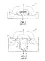
- FIG. 3is a schematic of a gate signal bus utilizing trenches in accordance with the preferred embodiment of the present invention, showing the mechanism for enhanced voltage protection.
- FIG. 3 ais a partial cutaway close-up schematic of the gate signal bus as shown in FIG. 3, showing the mechanism for enhanced voltage protection as it relates to trench spacing.
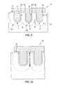
- FIGS. 4 a to 4 fare a series of schematics showing the trench process utilizing in a gate signal bus production according to the present invention.
- FIG. 3shows a power MOSFET gate signal bus 30 (shown simplified) utilizing trench technology.
- the gate signal bus 30includes trenches 31 , 32 , and 33 . These trenches 31 , 32 , and 33 are placed within an N+ substrate in parallel to one another and spaced apart by a distance X. Forming trenches 31 , 32 , and 33 in such a way creates a depletion region overlap 34 between adjacent trenches 31 , 32 and 33 so as to couple the depletion region 31 s with depletion region 32 a and depletion region 32 a with depletion region 33 a.
- gate signal bus 30is capable of withstanding voltages up to the maximum value supported by the underlying epitaxial layer 35 .
- the generation of the depletion regions 31 a, 32 a, and 33 ais a characteristic of all MOS structures and, in this case, is critical to the feasibility of the present invention.
- the nature of the depletion regions 31 a, 32 a, and 33 ais well understood and known to be dependent upon the applied voltage across the MOS system as well as the semiconductor dopant concentration. Accordingly, the spacing distance X between the trenches 31 , 32 , and 33 is related to the required specifications that any given final device demands.
- each of the depletion regions 31 a, 32 a, and 33 ahave a depletion region width Y that determines the electric field that exists across the region and hence the voltage drop. Therefore, any applied voltage beyond that voltage drop must be partially dropped across the thin gate oxide layer 36 . If this becomes too great, hot electron generation can occur, which can lead to an irreversible device breakdown.
- a thick layer of thermally grown silicon dioxide(not shown) is typically placed underneath the gate oxide layer 36 to prevent such breakdowns in planar structures and single trench structures, such an additional layer is typically both time consuming and costly. This extra layer is unnecessary in the present invention as illustrated in FIG. 3 because the overlap 34 of the depletion regions effectively extends the space charge boundary 37 , as shown in FIG. 3 a, due to the trench field coupling.
- FIG. 3 aillustrates a section 30 a of the gate signal bus 30 shown in FIG. 3 .
- FIGS. 4 a through 4 fare a series of schematics showing steps in the production of a field coupled power MOSFET bus using trench technology in accordance with the preferred embodiment of the present invention.
- a silicon surface 40is shown having been formed with spaced-apart trenches 41 . Any suitable method of formation may be utilized such as photoresist mask deposition with anisotropic etching.
- a central group 42 of closely aligned trenches 41is formed. This central group 42 is the initial structure required to form a gate bus. Each trench 41 within the central group 42 is spaced apart by a predetermined distance X as discussed above with respect to FIG. 3 .
- the distance Xis determined by the electrical characteristics (i.e., its breakdown voltage value).
- a gate oxide layer 43is shown as having been formed on the exposed top-portions of the silicon surface 40 .
- the gate oxide layer 43is a relatively thin layer (preferably 400 ⁇ ) of silicon dioxide.
- a total depth 44 from the top edge of the gate oxide layer 43 to the bottom trench edgeis approximately 2.0 microns in this case, but is dependent on, and hence can change with, the device's breakdown voltage.
- the trenches 41are etched and the gate oxide layer 43 are uniformly grown over the silicon surface 40 by any well known methods—e.g., photomasking and thermal cycling.
- each trench 41is back-filled with N type polysilicon 45 .
- surface structures 46 a, 46 b, and 46 care formed, also from N type polysilicon 45 .
- Surface structure 46 bis formed so as to be uniformly aligned above the central group of trenches 42 . This surface structure 46 b formed above the central group 42 is spaced by a gap 47 from the two laterally-placed surface structures 46 a and 46 c.
- These surface structures 46 a, 46 b, and 46 care formed with one trench set aligned in the area between each surface pair, i.e., 45 between 46 a and 46 b and between 46 ba and 46 c in preparation of the formation of active MOS transistor devices.
- FIG. 4 dillustrates well formation through the gaps 47 .
- Ion implantsare illustrated by arrows 48 .
- ion implants 48are utilized with thermal diffusion to distribute dopant and remove defects so as to form P type wells 49 (Pwells) and N type well (Nwells).
- PwellsP type wells 49
- NwellsN type well
- Commonly used boron implants and arsenic implantsare utilized in the well formation, utilizing any suitable prior art method and are not critical for purposes of disclosing the present invention.
- the P type wells 49include channel (P ⁇ ) and heavy body (P+) material (as also detailed in FIG. 2 ).
- the N type wells 50are formed as source (N+) material.
- an interlayer dielectric 51is shown deposited on the silicon surface 40 so as to surround each of the surface structures 46 a, 46 b, and 46 c.
- the dielectric 51is preferably boronphosphosilicate glass a (BPSG), but phosphosilicate glass (PSG) may alternatively be used.
- BPSGboronphosphosilicate glass a
- PSGphosphosilicate glass
- the dielectric 51is patterned in such a way so as to form source-metal-contact regions 52 a and 52 b.
- Subsequent well-known trench DMOS fabrication stepsinclude the formation of contact ports for forming electrical connection on the double-diffused active devices associated with openings 52 a and 52 b while isolating the polysilicon material 45 of the trenches therefrom Deposition of a top metal 53 to thereby form sources 54 a and 54 b is shown in FIG. 4 f. Between sources 54 a and 54 b, there is formed a trench gate signal bus region 55 formed by the gates 58 . It can be seen that through layer 46 b, all of the individual gates are connected together to establish the single trench gate signal bus region 55 .
- a double-diffused MOS deviceis thereby formed by the double diffusion of regions 49 and 50 to form the active source regions, and the non-double diffused gate signal bus associated with region 55 .
- a critical distinguishing feature of the present inventionis the current conduction path shown by arrows 59 .
- the current conduction path 59 of the present inventive designis vertically aligned through the epitaxial and substrate layers. The channel junctions are self-aligned to the polysilicon and trenches.
Landscapes
- Insulated Gate Type Field-Effect Transistor (AREA)
- Electrodes Of Semiconductors (AREA)
- Metal-Oxide And Bipolar Metal-Oxide Semiconductor Integrated Circuits (AREA)
- Thyristors (AREA)
Abstract
Description
Claims (6)
Priority Applications (1)
| Application Number | Priority Date | Filing Date | Title |
|---|---|---|---|
| US10/105,721US6673680B2 (en) | 1998-01-27 | 2002-03-25 | Field coupled power MOSFET bus architecture using trench technology |
Applications Claiming Priority (2)
| Application Number | Priority Date | Filing Date | Title |
|---|---|---|---|
| US09/014,115US6396102B1 (en) | 1998-01-27 | 1998-01-27 | Field coupled power MOSFET bus architecture using trench technology |
| US10/105,721US6673680B2 (en) | 1998-01-27 | 2002-03-25 | Field coupled power MOSFET bus architecture using trench technology |
Related Parent Applications (1)
| Application Number | Title | Priority Date | Filing Date |
|---|---|---|---|
| US09/014,115DivisionUS6396102B1 (en) | 1998-01-27 | 1998-01-27 | Field coupled power MOSFET bus architecture using trench technology |
Publications (2)
| Publication Number | Publication Date |
|---|---|
| US20020102795A1 US20020102795A1 (en) | 2002-08-01 |
| US6673680B2true US6673680B2 (en) | 2004-01-06 |
Family
ID=21763629
Family Applications (2)
| Application Number | Title | Priority Date | Filing Date |
|---|---|---|---|
| US09/014,115Expired - LifetimeUS6396102B1 (en) | 1998-01-27 | 1998-01-27 | Field coupled power MOSFET bus architecture using trench technology |
| US10/105,721Expired - LifetimeUS6673680B2 (en) | 1998-01-27 | 2002-03-25 | Field coupled power MOSFET bus architecture using trench technology |
Family Applications Before (1)
| Application Number | Title | Priority Date | Filing Date |
|---|---|---|---|
| US09/014,115Expired - LifetimeUS6396102B1 (en) | 1998-01-27 | 1998-01-27 | Field coupled power MOSFET bus architecture using trench technology |
Country Status (4)
| Country | Link |
|---|---|
| US (2) | US6396102B1 (en) |
| JP (1) | JPH11284174A (en) |
| DE (1) | DE19901386A1 (en) |
| FR (1) | FR2776837A1 (en) |
Cited By (23)
| Publication number | Priority date | Publication date | Assignee | Title |
|---|---|---|---|---|
| US20040173844A1 (en)* | 2003-03-05 | 2004-09-09 | Advanced Analogic Technologies, Inc. Advanced Analogic Technologies (Hongkong) Limited | Trench power MOSFET with planarized gate bus |
| US20050224887A1 (en)* | 2004-04-09 | 2005-10-13 | Kabushiki Kaisha Toshiba | Semiconductor device for power MOS transistor module |
| US20050287721A1 (en)* | 2004-06-28 | 2005-12-29 | Semiconductor Energy Laboratory Co., Ltd. | Method for manufacturing wiring substrate, thin film transistor, display device and television device |
| US20060158482A1 (en)* | 2003-04-25 | 2006-07-20 | Semiconductor Energy Laboratory Co., Ltd. | Drop discharge apparatus, method for forming pattern and method for manufacturing semiconductor device |
| US20070155104A1 (en)* | 2006-01-05 | 2007-07-05 | Marchant Bruce D | Power device utilizing chemical mechanical planarization |
| US20080012569A1 (en)* | 2005-05-21 | 2008-01-17 | Hall David R | Downhole Coils |
| US20080012076A1 (en)* | 2004-01-26 | 2008-01-17 | Semiconductor Energy Laboratory Co., Ltd. | Display device, method for manufacturing thereof, and television device |
| US20080081423A1 (en)* | 2006-09-29 | 2008-04-03 | Sadwick Laurence P | Processes and packaging for high voltage integrated circuits, electronic devices, and circuits |
| CN100388445C (en)* | 2004-12-08 | 2008-05-14 | 上海华虹Nec电子有限公司 | Manufacturing method of high-power MOS tube with small line width trench structure |
| KR100897820B1 (en) | 2007-07-26 | 2009-05-15 | 주식회사 동부하이텍 | Semiconductor device and its manufacturing method |
| US20100051943A1 (en)* | 2004-03-24 | 2010-03-04 | Semiconductor Energy Laboratory Co. Ltd. | Method for forming pattern, thin film transistor, display device, method for manufacturing thereof, and television apparatus |
| US20100140689A1 (en)* | 2008-12-08 | 2010-06-10 | Yedinak Joseph A | Trench-Based Power Semiconductor Devices with Increased Breakdown Voltage Characteristics |
| US20100140695A1 (en)* | 2008-12-08 | 2010-06-10 | Yedinak Joseph A | Trench-Based Power Semiconductor Devices With Increased Breakdown Voltage Characteristics |
| US20100200910A1 (en)* | 2009-02-09 | 2010-08-12 | Joseph Yedinak | Semiconductor Devices with Stable and Controlled Avalanche Characteristics and Methods of Fabricating the Same |
| US20100207205A1 (en)* | 2009-02-19 | 2010-08-19 | Grebs Thomas E | Structures and Methods for Improving Trench-Shielded Semiconductor Devices and Schottky Barrier Rectifier Devices |
| US7812355B2 (en) | 2004-03-03 | 2010-10-12 | Semiconductor Energy Laboratory Co., Ltd. | Semiconductor device and method for manufacturing the same, liquid crystal television, and EL television |
| US20100314707A1 (en)* | 2009-06-12 | 2010-12-16 | Yedinak Joseph A | Reduced Process Sensitivity of Electrode-Semiconductor Rectifiers |
| US20120161286A1 (en)* | 2010-12-23 | 2012-06-28 | Anup Bhalla | Monolithic IGBT and diode structure for quasi-resonant converters |
| US8786045B2 (en) | 2003-05-20 | 2014-07-22 | Fairchild Semiconductor Corporation | Power semiconductor devices having termination structures |
| US8872278B2 (en) | 2011-10-25 | 2014-10-28 | Fairchild Semiconductor Corporation | Integrated gate runner and field implant termination for trench devices |
| US20140342556A1 (en)* | 2013-05-20 | 2014-11-20 | Globalfoundries Inc. | Reusing active area mask for trench transfer exposure |
| US8928077B2 (en) | 2007-09-21 | 2015-01-06 | Fairchild Semiconductor Corporation | Superjunction structures for power devices |
| US9613892B2 (en) | 2014-10-31 | 2017-04-04 | Hamilton Sundstrand Corporation | Solid state contactor with improved interconnect structure |
Families Citing this family (23)
| Publication number | Priority date | Publication date | Assignee | Title |
|---|---|---|---|---|
| US7084456B2 (en)* | 1999-05-25 | 2006-08-01 | Advanced Analogic Technologies, Inc. | Trench MOSFET with recessed clamping diode using graded doping |
| JP4128700B2 (en)* | 1999-09-08 | 2008-07-30 | ローム株式会社 | Inductive load drive circuit |
| JP3679954B2 (en)* | 1999-09-24 | 2005-08-03 | 株式会社東芝 | Semiconductor device |
| US6838735B1 (en)* | 2000-02-24 | 2005-01-04 | International Rectifier Corporation | Trench FET with non overlapping poly and remote contact therefor |
| US6921939B2 (en)* | 2000-07-20 | 2005-07-26 | Fairchild Semiconductor Corporation | Power MOSFET and method for forming same using a self-aligned body implant |
| CN1187839C (en)* | 2001-01-19 | 2005-02-02 | 三菱电机株式会社 | Semiconductor device |
| US7132712B2 (en) | 2002-11-05 | 2006-11-07 | Fairchild Semiconductor Corporation | Trench structure having one or more diodes embedded therein adjacent a PN junction |
| GB0122120D0 (en) | 2001-09-13 | 2001-10-31 | Koninkl Philips Electronics Nv | Edge termination in MOS transistors |
| US7061066B2 (en) | 2001-10-17 | 2006-06-13 | Fairchild Semiconductor Corporation | Schottky diode using charge balance structure |
| DE10164486A1 (en)* | 2001-12-29 | 2003-07-17 | Bosch Gmbh Robert | Device for controlling an electrical power component |
| FR2859731B1 (en) | 2003-09-16 | 2008-03-07 | Arkema | COMPOSITIONS BASED ON FLUORINATED HYDROCARBONS AND SECONDARY BUTANOL FOR THE DEFLUXING OF ELECTRONIC CARDS |
| DE10353387B4 (en)* | 2003-11-14 | 2008-07-24 | Infineon Technologies Ag | Method for producing a power transistor arrangement and power transistor arrangement |
| US7462908B2 (en)* | 2004-07-14 | 2008-12-09 | International Rectifier Corporation | Dynamic deep depletion field effect transistor |
| US7352036B2 (en) | 2004-08-03 | 2008-04-01 | Fairchild Semiconductor Corporation | Semiconductor power device having a top-side drain using a sinker trench |
| CN101185169B (en) | 2005-04-06 | 2010-08-18 | 飞兆半导体公司 | Trench gate field effect transistor and method of forming the same |
| DE102005028224B4 (en)* | 2005-06-17 | 2015-08-20 | Infineon Technologies Ag | Semiconductor device with a transistor |
| US20090098701A1 (en)* | 2007-10-15 | 2009-04-16 | Jurgen Faul | Method of manufacturing an integrated circuit |
| US8912621B1 (en)* | 2011-07-11 | 2014-12-16 | Diodes Incorporated | Trench schottky devices |
| US9130060B2 (en) | 2012-07-11 | 2015-09-08 | Taiwan Semiconductor Manufacturing Company, Ltd. | Integrated circuit having a vertical power MOS transistor |
| US8669611B2 (en) | 2012-07-11 | 2014-03-11 | Taiwan Semiconductor Manufacturing Company, Ltd. | Apparatus and method for power MOS transistor |
| DE102013108518B4 (en)* | 2013-08-07 | 2016-11-24 | Infineon Technologies Ag | SEMICONDUCTOR DEVICE AND METHOD FOR MANUFACTURING THE SAME |
| JP6946764B2 (en)* | 2017-06-09 | 2021-10-06 | 富士電機株式会社 | Semiconductor devices and manufacturing methods for semiconductor devices |
| US10438813B2 (en) | 2017-11-13 | 2019-10-08 | Alpha And Omega Semiconductor (Cayman) Ltd. | Semiconductor device having one or more titanium interlayers and method of making the same |
Citations (13)
| Publication number | Priority date | Publication date | Assignee | Title |
|---|---|---|---|---|
| JPS5718365A (en) | 1980-07-08 | 1982-01-30 | Matsushita Electronics Corp | Semiconductor device and manufacture thereof |
| US4697201A (en) | 1981-12-18 | 1987-09-29 | Nissan Motor Company, Limited | Power MOS FET with decreased resistance in the conducting state |
| US4914058A (en) | 1987-12-29 | 1990-04-03 | Siliconix Incorporated | Grooved DMOS process with varying gate dielectric thickness |
| US4942445A (en)* | 1988-07-05 | 1990-07-17 | General Electric Company | Lateral depletion mode tyristor |
| US4994883A (en)* | 1989-10-02 | 1991-02-19 | General Electric Company | Field controlled diode (FCD) having MOS trench gates |
| US5072266A (en)* | 1988-12-27 | 1991-12-10 | Siliconix Incorporated | Trench DMOS power transistor with field-shaping body profile and three-dimensional geometry |
| EP0594177A1 (en) | 1992-10-22 | 1994-04-27 | Kabushiki Kaisha Toshiba | Vertical MOSFET having trench covered with multilayer gate film |
| US5541430A (en) | 1992-06-12 | 1996-07-30 | Mitsubishi Denki Kabushiki Kaisha | VDMOS semiconductor device |
| US5557127A (en) | 1995-03-23 | 1996-09-17 | International Rectifier Corporation | Termination structure for mosgated device with reduced mask count and process for its manufacture |
| US5602046A (en) | 1996-04-12 | 1997-02-11 | National Semiconductor Corporation | Integrated zener diode protection structures and fabrication methods for DMOS power devices |
| US5665996A (en) | 1994-12-30 | 1997-09-09 | Siliconix Incorporated | Vertical power mosfet having thick metal layer to reduce distributed resistance |
| US5894149A (en) | 1996-04-11 | 1999-04-13 | Mitsubishi Denki Kabushiki Kaisha | Semiconductor device having high breakdown voltage and method of manufacturing the same |
| US5972741A (en) | 1996-10-31 | 1999-10-26 | Sanyo Electric Co., Ltd. | Method of manufacturing semiconductor device |
- 1998
- 1998-01-27USUS09/014,115patent/US6396102B1/ennot_activeExpired - Lifetime
- 1999
- 1999-01-15DEDE19901386Apatent/DE19901386A1/ennot_activeWithdrawn
- 1999-01-25FRFR9900780Apatent/FR2776837A1/enactivePending
- 1999-01-27JPJP11019040Apatent/JPH11284174A/enactivePending
- 2002
- 2002-03-25USUS10/105,721patent/US6673680B2/ennot_activeExpired - Lifetime
Patent Citations (14)
| Publication number | Priority date | Publication date | Assignee | Title |
|---|---|---|---|---|
| JPS5718365A (en) | 1980-07-08 | 1982-01-30 | Matsushita Electronics Corp | Semiconductor device and manufacture thereof |
| US4697201A (en) | 1981-12-18 | 1987-09-29 | Nissan Motor Company, Limited | Power MOS FET with decreased resistance in the conducting state |
| US4914058A (en) | 1987-12-29 | 1990-04-03 | Siliconix Incorporated | Grooved DMOS process with varying gate dielectric thickness |
| US4942445A (en)* | 1988-07-05 | 1990-07-17 | General Electric Company | Lateral depletion mode tyristor |
| US5072266A (en)* | 1988-12-27 | 1991-12-10 | Siliconix Incorporated | Trench DMOS power transistor with field-shaping body profile and three-dimensional geometry |
| US4994883A (en)* | 1989-10-02 | 1991-02-19 | General Electric Company | Field controlled diode (FCD) having MOS trench gates |
| US5541430A (en) | 1992-06-12 | 1996-07-30 | Mitsubishi Denki Kabushiki Kaisha | VDMOS semiconductor device |
| EP0594177A1 (en) | 1992-10-22 | 1994-04-27 | Kabushiki Kaisha Toshiba | Vertical MOSFET having trench covered with multilayer gate film |
| US5321289A (en) | 1992-10-22 | 1994-06-14 | Kabushiki Kaisha Toshiba | Vertical MOSFET having trench covered with multilayer gate film |
| US5665996A (en) | 1994-12-30 | 1997-09-09 | Siliconix Incorporated | Vertical power mosfet having thick metal layer to reduce distributed resistance |
| US5557127A (en) | 1995-03-23 | 1996-09-17 | International Rectifier Corporation | Termination structure for mosgated device with reduced mask count and process for its manufacture |
| US5894149A (en) | 1996-04-11 | 1999-04-13 | Mitsubishi Denki Kabushiki Kaisha | Semiconductor device having high breakdown voltage and method of manufacturing the same |
| US5602046A (en) | 1996-04-12 | 1997-02-11 | National Semiconductor Corporation | Integrated zener diode protection structures and fabrication methods for DMOS power devices |
| US5972741A (en) | 1996-10-31 | 1999-10-26 | Sanyo Electric Co., Ltd. | Method of manufacturing semiconductor device |
Non-Patent Citations (2)
| Title |
|---|
| Baba, et al, "A Study on High Blocking Voltage UMOS-FET With a Double Gate Structure", Published May 19, 1992 & Presented at 1992 International Symposium on Power Semiconductor Devices & ICs, Tokyo, pp. 300-302. |
| Goodenough, Frank, "Small Packages on Tap for Low-Voltage Power MOSFETs", Electronic Design, pp. 103-110, (Jun. 9, 1997). |
Cited By (65)
| Publication number | Priority date | Publication date | Assignee | Title |
|---|---|---|---|---|
| US20060014349A1 (en)* | 2003-03-05 | 2006-01-19 | Williams Richard K | Planarized and silicided trench contact |
| US20040173844A1 (en)* | 2003-03-05 | 2004-09-09 | Advanced Analogic Technologies, Inc. Advanced Analogic Technologies (Hongkong) Limited | Trench power MOSFET with planarized gate bus |
| US20040183136A1 (en)* | 2003-03-05 | 2004-09-23 | Williams Richard K. | Planarized and silicided trench contact |
| US6861701B2 (en)* | 2003-03-05 | 2005-03-01 | Advanced Analogic Technologies, Inc. | Trench power MOSFET with planarized gate bus |
| US6969888B2 (en)* | 2003-03-05 | 2005-11-29 | Advanced Analogic Technologies, Inc. | Planarized and silicided trench contact |
| US7075145B2 (en) | 2003-03-05 | 2006-07-11 | Advanced Analogic Technologies, Inc. | Poly-sealed silicide trench gate |
| US20040183129A1 (en)* | 2003-03-05 | 2004-09-23 | Williams Richard K. | Poly-sealed silicide trench gate |
| US7419878B2 (en) | 2003-03-05 | 2008-09-02 | Advanced Analogic Technologies, Inc. | Planarized and silicided trench contact |
| US20090314203A1 (en)* | 2003-04-25 | 2009-12-24 | Semiconductor Energy Laboratory Co., Ltd. | Drop discharge apparatus, method for forming pattern and method for manufacturing semiconductor device |
| US20060158482A1 (en)* | 2003-04-25 | 2006-07-20 | Semiconductor Energy Laboratory Co., Ltd. | Drop discharge apparatus, method for forming pattern and method for manufacturing semiconductor device |
| US7585783B2 (en)* | 2003-04-25 | 2009-09-08 | Semiconductor Energy Laboratory Co., Ltd. | Drop discharge apparatus, method for forming pattern and method for manufacturing semiconductor device |
| US8528497B2 (en) | 2003-04-25 | 2013-09-10 | Semiconductor Energy Laboratory Co., Ltd. | Drop discharge apparatus, method for forming pattern and method for manufacturing semiconductor device |
| US8786045B2 (en) | 2003-05-20 | 2014-07-22 | Fairchild Semiconductor Corporation | Power semiconductor devices having termination structures |
| US20080012076A1 (en)* | 2004-01-26 | 2008-01-17 | Semiconductor Energy Laboratory Co., Ltd. | Display device, method for manufacturing thereof, and television device |
| US8518760B2 (en) | 2004-01-26 | 2013-08-27 | Semiconductor Energy Co., Ltd. | Display device, method for manufacturing thereof, and television device |
| US7939888B2 (en) | 2004-01-26 | 2011-05-10 | Semiconductor Energy Laboratory Co., Ltd. | Display device and television device using the same |
| US20110165741A1 (en)* | 2004-01-26 | 2011-07-07 | Semiconductor Energy Laboratory Co., Ltd. | Display device, method for manufacturing thereof, and television device |
| US7812355B2 (en) | 2004-03-03 | 2010-10-12 | Semiconductor Energy Laboratory Co., Ltd. | Semiconductor device and method for manufacturing the same, liquid crystal television, and EL television |
| US20100051943A1 (en)* | 2004-03-24 | 2010-03-04 | Semiconductor Energy Laboratory Co. Ltd. | Method for forming pattern, thin film transistor, display device, method for manufacturing thereof, and television apparatus |
| US8222636B2 (en) | 2004-03-24 | 2012-07-17 | Semiconductor Energy Laboratory Co., Ltd. | Method for forming pattern, thin film transistor, display device, method for manufacturing thereof, and television apparatus |
| US6992351B2 (en)* | 2004-04-09 | 2006-01-31 | Kabushiki Kaisha Toshiba | Semiconductor device for power MOS transistor module |
| US20050224887A1 (en)* | 2004-04-09 | 2005-10-13 | Kabushiki Kaisha Toshiba | Semiconductor device for power MOS transistor module |
| US20050287721A1 (en)* | 2004-06-28 | 2005-12-29 | Semiconductor Energy Laboratory Co., Ltd. | Method for manufacturing wiring substrate, thin film transistor, display device and television device |
| US8158517B2 (en) | 2004-06-28 | 2012-04-17 | Semiconductor Energy Laboratory Co., Ltd. | Method for manufacturing wiring substrate, thin film transistor, display device and television device |
| CN100388445C (en)* | 2004-12-08 | 2008-05-14 | 上海华虹Nec电子有限公司 | Manufacturing method of high-power MOS tube with small line width trench structure |
| US20080012569A1 (en)* | 2005-05-21 | 2008-01-17 | Hall David R | Downhole Coils |
| US20070155104A1 (en)* | 2006-01-05 | 2007-07-05 | Marchant Bruce D | Power device utilizing chemical mechanical planarization |
| US7772642B2 (en) | 2006-01-05 | 2010-08-10 | Fairchild Semiconductor Corporation | Power trench gate FET with active gate trenches that are contiguous with gate runner trench |
| US8461040B2 (en) | 2006-01-05 | 2013-06-11 | Fairchild Semiconductor Corporation | Method of forming shielded gate power transistor utilizing chemical mechanical planarization |
| US7449354B2 (en) | 2006-01-05 | 2008-11-11 | Fairchild Semiconductor Corporation | Trench-gated FET for power device with active gate trenches and gate runner trench utilizing one-mask etch |
| US20090020810A1 (en)* | 2006-01-05 | 2009-01-22 | Bruce Douglas Marchant | Method of Forming Power Device Utilizing Chemical Mechanical Planarization |
| US7902071B2 (en) | 2006-01-05 | 2011-03-08 | Fairchild Semiconductor Corporation | Method for forming active and gate runner trenches |
| US7709292B2 (en) | 2006-09-29 | 2010-05-04 | Sadwick Laurence P | Processes and packaging for high voltage integrated circuits, electronic devices, and circuits |
| US20080081423A1 (en)* | 2006-09-29 | 2008-04-03 | Sadwick Laurence P | Processes and packaging for high voltage integrated circuits, electronic devices, and circuits |
| KR100897820B1 (en) | 2007-07-26 | 2009-05-15 | 주식회사 동부하이텍 | Semiconductor device and its manufacturing method |
| US8928077B2 (en) | 2007-09-21 | 2015-01-06 | Fairchild Semiconductor Corporation | Superjunction structures for power devices |
| US9595596B2 (en) | 2007-09-21 | 2017-03-14 | Fairchild Semiconductor Corporation | Superjunction structures for power devices |
| US20100140696A1 (en)* | 2008-12-08 | 2010-06-10 | Yedinak Joseph A | Trench-Based Power Semiconductor Devices With Increased Breakdown Voltage Characteristics |
| US9391193B2 (en) | 2008-12-08 | 2016-07-12 | Fairchild Semiconductor Corporation | Trench-based power semiconductor devices with increased breakdown voltage characteristics |
| US8174067B2 (en) | 2008-12-08 | 2012-05-08 | Fairchild Semiconductor Corporation | Trench-based power semiconductor devices with increased breakdown voltage characteristics |
| US8193581B2 (en) | 2008-12-08 | 2012-06-05 | Fairchild Semiconductor Corporation | Trench-based power semiconductor devices with increased breakdown voltage characteristics |
| US8563377B2 (en) | 2008-12-08 | 2013-10-22 | Fairchild Semiconductor Corporation | Trench-based power semiconductor devices with increased breakdown voltage characteristics |
| US20100140689A1 (en)* | 2008-12-08 | 2010-06-10 | Yedinak Joseph A | Trench-Based Power Semiconductor Devices with Increased Breakdown Voltage Characteristics |
| US10868113B2 (en) | 2008-12-08 | 2020-12-15 | Fairchild Semiconductor Corporation | Trench-based power semiconductor devices with increased breakdown voltage characteristics |
| US8304829B2 (en) | 2008-12-08 | 2012-11-06 | Fairchild Semiconductor Corporation | Trench-based power semiconductor devices with increased breakdown voltage characteristics |
| US9748329B2 (en) | 2008-12-08 | 2017-08-29 | Fairchild Semiconductor Corporation | Trench-based power semiconductor devices with increased breakdown voltage characteristics |
| US8564024B2 (en) | 2008-12-08 | 2013-10-22 | Fairchild Semiconductor Corporation | Trench-based power semiconductor devices with increased breakdown voltage characteristics |
| US9293526B2 (en) | 2008-12-08 | 2016-03-22 | Fairchild Semiconductor Corporation | Trench-based power semiconductor devices with increased breakdown voltage characteristics |
| US8963212B2 (en) | 2008-12-08 | 2015-02-24 | Fairchild Semiconductor Corporation | Trench-based power semiconductor devices with increased breakdown voltage characteristics |
| US8932924B2 (en) | 2008-12-08 | 2015-01-13 | Fairchild Semiconductor Corporation | Trench-based power semiconductor devices with increased breakdown voltage characteristics |
| US20100140697A1 (en)* | 2008-12-08 | 2010-06-10 | Yedinak Joseph A | Trench-Based Power Semiconductor Devices with Increased Breakdown Voltage Characteristics |
| US20100140695A1 (en)* | 2008-12-08 | 2010-06-10 | Yedinak Joseph A | Trench-Based Power Semiconductor Devices With Increased Breakdown Voltage Characteristics |
| US20100200910A1 (en)* | 2009-02-09 | 2010-08-12 | Joseph Yedinak | Semiconductor Devices with Stable and Controlled Avalanche Characteristics and Methods of Fabricating the Same |
| US8227855B2 (en) | 2009-02-09 | 2012-07-24 | Fairchild Semiconductor Corporation | Semiconductor devices with stable and controlled avalanche characteristics and methods of fabricating the same |
| US20100207205A1 (en)* | 2009-02-19 | 2010-08-19 | Grebs Thomas E | Structures and Methods for Improving Trench-Shielded Semiconductor Devices and Schottky Barrier Rectifier Devices |
| US8148749B2 (en) | 2009-02-19 | 2012-04-03 | Fairchild Semiconductor Corporation | Trench-shielded semiconductor device |
| US20100314707A1 (en)* | 2009-06-12 | 2010-12-16 | Yedinak Joseph A | Reduced Process Sensitivity of Electrode-Semiconductor Rectifiers |
| US8492837B2 (en) | 2009-06-12 | 2013-07-23 | Fairchild Semiconductor Corporation | Reduced process sensitivity of electrode-semiconductor rectifiers |
| US8049276B2 (en) | 2009-06-12 | 2011-11-01 | Fairchild Semiconductor Corporation | Reduced process sensitivity of electrode-semiconductor rectifiers |
| US8502346B2 (en)* | 2010-12-23 | 2013-08-06 | Alpha And Omega Semiconductor Incorporated | Monolithic IGBT and diode structure for quasi-resonant converters |
| US20120161286A1 (en)* | 2010-12-23 | 2012-06-28 | Anup Bhalla | Monolithic IGBT and diode structure for quasi-resonant converters |
| US8872278B2 (en) | 2011-10-25 | 2014-10-28 | Fairchild Semiconductor Corporation | Integrated gate runner and field implant termination for trench devices |
| US8962485B2 (en)* | 2013-05-20 | 2015-02-24 | Globalfoundries Inc. | Reusing active area mask for trench transfer exposure |
| US20140342556A1 (en)* | 2013-05-20 | 2014-11-20 | Globalfoundries Inc. | Reusing active area mask for trench transfer exposure |
| US9613892B2 (en) | 2014-10-31 | 2017-04-04 | Hamilton Sundstrand Corporation | Solid state contactor with improved interconnect structure |
Also Published As
| Publication number | Publication date |
|---|---|
| JPH11284174A (en) | 1999-10-15 |
| US6396102B1 (en) | 2002-05-28 |
| FR2776837A1 (en) | 1999-10-01 |
| US20020102795A1 (en) | 2002-08-01 |
| DE19901386A1 (en) | 1999-09-23 |
Similar Documents
| Publication | Publication Date | Title |
|---|---|---|
| US6673680B2 (en) | Field coupled power MOSFET bus architecture using trench technology | |
| US5897343A (en) | Method of making a power switching trench MOSFET having aligned source regions | |
| US6468866B2 (en) | Single feature size MOS technology power device | |
| US5879994A (en) | Self-aligned method of fabricating terrace gate DMOS transistor | |
| KR100415490B1 (en) | Power mos element and method for producing the same | |
| US7186618B2 (en) | Power transistor arrangement and method for fabricating it | |
| US7989886B2 (en) | Alignment of trench for MOS | |
| US6117738A (en) | Method for fabricating a high-bias semiconductor device | |
| KR20060111859A (en) | Semiconductor device and method with screening electrodes | |
| US6548864B2 (en) | High density MOS technology power device | |
| US6160288A (en) | Vertical type misfet having improved pressure resistance | |
| US6674123B2 (en) | MOS control diode and method for manufacturing the same | |
| EP1535344B1 (en) | Vertical gate semiconductor device with a self-aligned structure | |
| JP2006510206A (en) | Integrated circuit structure | |
| US7205605B2 (en) | Semiconductor component and method of manufacturing | |
| US5844277A (en) | Power MOSFETs and cell topology | |
| JP3489362B2 (en) | Semiconductor device and manufacturing method thereof | |
| US20230261085A1 (en) | Fabrication method of forming silicon carbide mosfet | |
| JP2003174164A (en) | Vertical MOS semiconductor device and method of manufacturing the same | |
| EP0568692B1 (en) | Power fet with shielded channels | |
| US6420756B1 (en) | Semiconductor device and method | |
| EP0791965A2 (en) | Vertical four terminal transistor | |
| HK1081325B (en) | Vertical gate semiconductor device with a self-aligned structure | |
| HK1097098B (en) | Semiconductor device having screening electrode and method |
Legal Events
| Date | Code | Title | Description |
|---|---|---|---|
| AS | Assignment | Owner name:FAIRCHILD SEMICONDUCTOR CORPORATION, MAINE Free format text:ASSIGNMENT OF ASSIGNORS INTEREST;ASSIGNOR:CALAFUT, DANIEL S.;REEL/FRAME:012739/0627 Effective date:20020320 | |
| STCF | Information on status: patent grant | Free format text:PATENTED CASE | |
| FPAY | Fee payment | Year of fee payment:4 | |
| FPAY | Fee payment | Year of fee payment:8 | |
| FPAY | Fee payment | Year of fee payment:12 | |
| AS | Assignment | Owner name:DEUTSCHE BANK AG NEW YORK BRANCH, AS COLLATERAL AGENT, NEW YORK Free format text:PATENT SECURITY AGREEMENT;ASSIGNOR:FAIRCHILD SEMICONDUCTOR CORPORATION;REEL/FRAME:040075/0644 Effective date:20160916 Owner name:DEUTSCHE BANK AG NEW YORK BRANCH, AS COLLATERAL AG Free format text:PATENT SECURITY AGREEMENT;ASSIGNOR:FAIRCHILD SEMICONDUCTOR CORPORATION;REEL/FRAME:040075/0644 Effective date:20160916 | |
| AS | Assignment | Owner name:SEMICONDUCTOR COMPONENTS INDUSTRIES, LLC, ARIZONA Free format text:ASSIGNMENT OF ASSIGNORS INTEREST;ASSIGNOR:FAIRCHILD SEMICONDUCTOR CORPORATION;REEL/FRAME:057694/0374 Effective date:20210722 | |
| AS | Assignment | Owner name:FAIRCHILD SEMICONDUCTOR CORPORATION, ARIZONA Free format text:RELEASE BY SECURED PARTY;ASSIGNOR:DEUTSCHE BANK AG NEW YORK BRANCH;REEL/FRAME:057969/0206 Effective date:20211027 | |
| AS | Assignment | Owner name:DEUTSCHE BANK AG NEW YORK BRANCH, AS COLLATERAL AGENT, NEW YORK Free format text:SECURITY INTEREST;ASSIGNOR:SEMICONDUCTOR COMPONENTS INDUSTRIES, LLC;REEL/FRAME:058871/0799 Effective date:20211028 | |
| AS | Assignment | Owner name:FAIRCHILD SEMICONDUCTOR CORPORATION, ARIZONA Free format text:RELEASE OF SECURITY INTEREST IN PATENTS RECORDED AT REEL 040075, FRAME 0644;ASSIGNOR:DEUTSCHE BANK AG NEW YORK BRANCH, AS COLLATERAL AGENT;REEL/FRAME:064070/0536 Effective date:20230622 Owner name:SEMICONDUCTOR COMPONENTS INDUSTRIES, LLC, ARIZONA Free format text:RELEASE OF SECURITY INTEREST IN PATENTS RECORDED AT REEL 040075, FRAME 0644;ASSIGNOR:DEUTSCHE BANK AG NEW YORK BRANCH, AS COLLATERAL AGENT;REEL/FRAME:064070/0536 Effective date:20230622 | |
| AS | Assignment | Owner name:FAIRCHILD SEMICONDUCTOR CORPORATION, ARIZONA Free format text:RELEASE OF SECURITY INTEREST IN PATENTS RECORDED AT REEL 058871, FRAME 0799;ASSIGNOR:DEUTSCHE BANK AG NEW YORK BRANCH, AS COLLATERAL AGENT;REEL/FRAME:065653/0001 Effective date:20230622 Owner name:SEMICONDUCTOR COMPONENTS INDUSTRIES, LLC, ARIZONA Free format text:RELEASE OF SECURITY INTEREST IN PATENTS RECORDED AT REEL 058871, FRAME 0799;ASSIGNOR:DEUTSCHE BANK AG NEW YORK BRANCH, AS COLLATERAL AGENT;REEL/FRAME:065653/0001 Effective date:20230622 |