US6673653B2 - Wafer-interposer using a ceramic substrate - Google Patents
Wafer-interposer using a ceramic substrateDownload PDFInfo
- Publication number
- US6673653B2 US6673653B2US09/792,257US79225701AUS6673653B2US 6673653 B2US6673653 B2US 6673653B2US 79225701 AUS79225701 AUS 79225701AUS 6673653 B2US6673653 B2US 6673653B2
- Authority
- US
- United States
- Prior art keywords
- recited
- ceramic substrate
- electrical contacts
- semiconductor wafer
- testing
- Prior art date
- Legal status (The legal status is an assumption and is not a legal conclusion. Google has not performed a legal analysis and makes no representation as to the accuracy of the status listed.)
- Expired - Fee Related, expires
Links
Images
Classifications
- H—ELECTRICITY
- H01—ELECTRIC ELEMENTS
- H01L—SEMICONDUCTOR DEVICES NOT COVERED BY CLASS H10
- H01L23/00—Details of semiconductor or other solid state devices
- H01L23/48—Arrangements for conducting electric current to or from the solid state body in operation, e.g. leads, terminal arrangements ; Selection of materials therefor
- H01L23/488—Arrangements for conducting electric current to or from the solid state body in operation, e.g. leads, terminal arrangements ; Selection of materials therefor consisting of soldered or bonded constructions
- H01L23/498—Leads, i.e. metallisations or lead-frames on insulating substrates, e.g. chip carriers
- H01L23/49827—Via connections through the substrates, e.g. pins going through the substrate, coaxial cables
- H—ELECTRICITY
- H01—ELECTRIC ELEMENTS
- H01L—SEMICONDUCTOR DEVICES NOT COVERED BY CLASS H10
- H01L2924/00—Indexing scheme for arrangements or methods for connecting or disconnecting semiconductor or solid-state bodies as covered by H01L24/00
- H01L2924/0001—Technical content checked by a classifier
- H01L2924/0002—Not covered by any one of groups H01L24/00, H01L24/00 and H01L2224/00
Definitions
- the present inventionrelates generally to the field of integrated circuits, and more particularly, to an interposer assembly apparatus and method.
- Wire bondingis still the interconnection strategy most often used in the semiconductor industry today. But the growing demand for products that are smaller, faster, less expensive, more reliable and have a reduced thermal profile has pushed wire bonding technology to its limits (and beyond) thereby creating barriers to sustained product improvement and growth.
- the high-performance alternative to wire bonding techniquesare flip chip techniques, in which solder balls or bumps are attached to the input/output (I/O) pads of the die at the wafer level.
- the bumped dieis flipped over and attached to a substrate “face down,” rather than “face up” as with wire bonding.
- Flip chipsresolve many, if not all, of the problems introduced by wire bonding.
- flip chipshave fewer electrical interconnects than wire bonding, which results in improved reliability and fewer manufacturing steps, thereby reducing production costs.
- the face down mounting of a flip chip die on a substrateallows superior thermal management techniques to be deployed than those available in wire bonding.
- flip chipsallow I/O to be located essentially anywhere on the die, within the limits of substrate pitch technology and manufacturing equipment, instead of forcing I/O to the peripheral of the die as in wire bonding. This results in increased I/O density and system miniaturization.
- the dieare removed from the test fixture and either retailed as a Known Good Die (“KGD”) product or used by the manufacturer in an end product, such as a Flip Chip Module (“FCM”).
- the Flip Chip Modulemay constitute a subassembly in a larger system product. This Known Good Die process is inherently inefficient due to its complexity.
- the coefficient of thermal expansion (CTE), and the ability to be planed to a high degree of flatnessare two characteristics that are important when selecting a material to form an interposer substrate.
- the CTE of the material chosenshould be close to that of a silicon wafer if the end use will be subjected to a range of temperatures, and the planarity should be as flat as possible, in any event, at least as flat as the semiconductor wafer the interposer substrate will be attached to.
- the material used for the interposer substrateshould also be structurally sound and capable of being patterned with traces, connectivity pads and vias. It should also be capable of withstanding the temperatures required to solder the finished semiconductor circuit to a printed circuit board.
- the present inventionprovides a method and apparatus for testing semiconductor wafers that is simple and allows testing prior to dicing so that the need to temporarily package individual dies for testing is eliminated. As a result, the number of manufacturing steps is reduced, thus increasing first pass yields. In addition, manufacturing time is decreased, thereby improving cycle times and avoiding additional costs. Eliminating the need to singulate and package the dies before testing results in a significant cost avoidance opportunity for chip manufacturers. The fact that the use of the wafer-interposer accomplishes all of this while providing cost effective packaging is another substantial benefit of the present invention.
- the ceramic substrate of the present inventionhas a good coefficient of thermal expansion that is close to that of a silicon wafer. Moreover, the ceramic substrate can be planed to a high degree of flatness and is capable of being patterned with traces, connectivity pads and electrical passageways or vias. The ceramic substrate also is capable of withstanding the temperatures required to solder the finished semiconductor circuit to a printed circuit board.
- One form of the present inventionprovides an interposer substrate made of a ceramic material that has an upper and a lower surface. There are one or more first electrical contacts on the lower surface and one or more second electrical contacts on the upper surface. There are also one or more electrical pathways that connect the first and second electrical contacts.
- Another form of the present inventionprovides an interposer assembly that includes a ceramic substrate having an upper and a lower surface with one or more first electrical contacts on the lower surface and one or more second electrical contacts on the upper surface.
- One or more electrical pathwaysconnect the first and second electrical contacts.
- a semiconductor waferincluding one or more semiconductor dies, and having an upper surface and lower surface with one or more third electrical contacts on the first surface.
- a conductorelectrically connects each first electrical contact with a corresponding third electrical contact, and a layer of no-flow underfill is disposed between the upper surface of the semiconductor wafer and the lower surface of the ceramic substrate.
- Yet another form of the present inventionis a method for producing an interposer substrate that includes the steps of creating one or more electrical pathways passing through a ceramic substrate having an upper surface and a lower surface. One or more first electrical contacts are attached to the one or more electrical pathways on the lower surface of the ceramic substrate. One or more second electrical contacts are attached to the one or more electrical pathways on the upper surface of the ceramic substrate.
- Still another form of the present inventionprovides a method for producing an interposer assembly. It includes the steps of creating one or more electrical pathways passing through a ceramic substrate having an upper surface and a lower surface. One or more first electrical contacts are attached to the one or more electrical pathways on the lower surface of the ceramic substrate. One or more second electrical contacts are attached to the one or more electrical pathways on the upper surface of the ceramic substrate. A conductor and a no-flow underfill are deposited and the ceramic substrate is bonded to a semiconductor wafer such that the conductor and the no-flow underfill form an adhesive bond between the lower side of the ceramic substrate and the upper side of the semiconductor wafer.
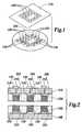
- FIG. 1depicts an exploded view of an interposer substrate and a semiconductor wafer in accordance with the present invention
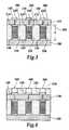
- FIG. 2depicts a side view of an interposer substrate and a semiconductor wafer prior to attachment in accordance with the present invention
- FIG. 3depicts a side view of an interposer substrate and a semiconductor wafer after attachment to form an interposer assembly in accordance with the present invention
- the present inventionprovides a method and apparatus for testing semiconductor wafers that is simple and allows testing prior to dicing so that the need to temporarily package individual dies for testing is eliminated. As a result, the number of manufacturing steps is reduced, thus increasing first pass yields. In addition, manufacturing time is decreased, thereby improving cycle times and avoiding additional costs. Eliminating the need to singulate and package the dies before testing results in a significant cost avoidance opportunity for chip manufacturers. The fact that the use of the wafer-interposer accomplishes all of this while providing cost effective packaging is another substantial benefit of the present invention.
- the ceramic substrate of the present inventionhas a good coefficient of thermal expansion that is close to that of a silicon wafer. Moreover, the ceramic substrate can be planed to a high degree of flatness and is capable of being patterned with traces, connectivity pads and electrical passageways or vias. The ceramic substrate also is capable of withstanding the temperatures required to solder the finished semiconductor circuit to a printed circuit board.
- the interposer assembly of the present inventionrevolutionizes the semiconductor fabrication process by enabling burn-in and electrical testing at the wafer level.
- the interposereliminates the need to singulate, package, test, and unpackage each die in order to arrive at the Known Good Die product stage.
- the interposerremains attached to the die following dicing, and thus provides the additional benefit of redistributing the die I/O pads so that they can be larger and more easily accessed and/or mated to other downstream components.
- FIG. 1depicts a semiconductor wafer 100 and a ceramic substrate 110 . When attached to one another, the pair forms an interposer assembly. An exploded view of a single die is shown on the semiconductor wafer 100 enclosed by a dotted line. The die has fourteen peripheral connection pads 120 . An actual wafer would have many more die and many more pads; the enlarged view is for illustrative purposes only.
- the larger pads 130are formed as part of a redistribution layer (RDL) that is added to the semiconductor wafer.
- the RDLconnects each peripheral connection pad 120 to an RDL pad 130 .
- the relationship between the peripheral and RDL padsis one-to-one, however other connectivity schemes are possible.
- Methods for designing and applying redistribution layersare well known in the industry. Because the RDL pads use the space in the center of the die, they can have greater size and pitch than the peripheral pads. The ability to use larger pads can be advantageous in compensating for thermal mismatches as discussed below. The larger pads also allow for easier connection to test equipment or printed circuit boards.
- FIG. 1also depicts a ceramic substrate 110 .
- the ceramic materialmay be chosen to meet the needs of a particular application. For example, if the circuit does not require burn-in or extended high or low temperature testing, then alumina may be an appropriate choice. Alumina is inexpensive, but it has a relatively high coefficient of thermal expansion that makes it a poor choice for applications that are exposed to large changes in temperature. Conversely, for extended temperature operation silicon nitride may be used. Silicon nitride more closely matches the coefficient of thermal expansion of a semiconductor wafer than does alumina, although it is more costly. There are no limitations on the nature of the ceramic used to form the interposer substrate of the present invention other than the requirements of the specific application envisioned.
- connection pads 140 on the upper surfaces of the ceramic substrate 110correspond with a second set of connectivity pads 210 on the lower surface of the ceramic substrate that in turn match up with the RDL pads on the semiconductor wafer 100 .
- the connectivity pads 210 on the lower surface of the ceramic substrateare not visible in FIG. 1 .
- the two sets of connectivity pads on the upper and lower surfaces of the ceramic substrateare connected by vias.
- the surfaces of the semiconductor wafer and the ceramic substrate that will meet when the interposer assembly is formedare very flat. Due to the nature of the processing involved to produce the semiconductor wafer, they are generally already very flat.
- the ceramic substratecan be polished on the lower surface in order to achieve approximately the same flatness as that of the semiconductor wafer. The polishing will be done prior to the addition of the connectivity pads to the lower surface of the ceramic substrate.
- FIG. 2depicts a side view of the semiconductor wafer 100 the ceramic substrate 110 after the application of a conductor 250 , 260 and a no-flow underfill 230 , 240 .
- the wafer and substrateare now ready to be joined to form an interposer assembly.
- the underfillis not cured.
- the conductor 250is applied to the pads 130 of the semiconductor wafer 100 .
- the method of applicationmay be screen printing, dispensing or any other method known in the industry.
- the material making up the conductormay be solder or conductive polymeric adhesive or conductive plastic.
- the height of the column of conductorwill be approximately equal to the diameter of the connectivity pad 130 .
- a layer of no-flow underfill 240is applied after the application of the conductor.
- Conductor 260is applied to connectivity pads 210 , followed by the application of no-flow underfill 230 .
- the column height of the conductoris approximately the same as the corresponding column of conductor applied to the semiconductor wafer 100 .
- the electrical pathways or vias 220 that connect the two sets of connectivity pads of the ceramic substrate 140 , 210are also depicted in FIG. 2 .
- FIG. 3depicts the ceramic substrate 110 connected to the semiconductor wafer 100 , thus forming an interposer assembly.
- the substrate and the waferare aligned and then brought together.
- Many means for alignmentmay be used, including aligning the edges of the respective components as well as the use of fiducials located on the wafers.
- Split vision opticsmay also be employed for alignment.
- the assemblyis then heated to fuse the two columns of conductor, if necessary, and to cure the underfill.
- a certain amount of “over travel”may be required to make sure that contact is made between all of the respective columns of conductor. This technique will compensate for slight differences in the height of the columns of conductor as well as minor deviations from planarity of either the ceramic substrate or the semiconductor wafer. If the exact distance required to bring the two tallest columns together is x as shown in FIG.
- the substrate and the waferwould be brought within x-y, where y is the difference between the tallest column of conductor and the shortest column. This would insure that all of the connections are made, and increase the production of good dies. The result would be that some of the columns would have excess conductor, but this would expand into the surrounding underfill and eventually produce a slightly wider column of conductor during the reflow and curing process.
- the connectivity pads 140are the points of connection when the die is eventually attached to a printed circuit board or other surface.
- the entire connection path of the interposer assemblyis defined starting with the peripheral connection pads 120 and proceeding through the RDL pads 130 , the columns of conductor 250 and 260 , to pads 210 , by way of the electrical pathways or vias 220 and ending at the connectivity pads 140 .
- the interposer assemblyis then heated reflow and cure and reflow the columns of conductor and to cure the underfill.
- the relatively tall columns of conductor in the completed interposer assemblythat are formed as a result of applying conductor to both the semiconductor wafer and the ceramic substrate prior to assembly, serve to compensate for thermal mismatches between the ceramic and wafer.
- the tall columncan adjust to any slight lateral movement cause by a thermal mismatch between the components.
- the underfillserves to suppress this lateral movement.
- the large connectivity pads 140 on the interposer assemblyfacilitate connection with burn-in boards or automated test equipment.
- the last test before the interposer assembly is diced into separate die unitsis to create a map of the die positions that indicates which are acceptable for further use. Following the dicing procedure the unacceptable units are culled and discarded.
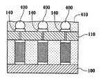
- solder bumps 400are applied to pads 140 after testing.
- FIG. 4depicts the interposer assembly following testing where the solder bumps have been applied, as well as a layer of low-melting underfill 410 .
- the low-melting underfillis chosen so that it is a solid at room temperature, but that during attachment of the circuit to a printed circuit board or other surface, it will flow at the same temperature as the solder bumps in order to assure good adhesion.
- the low-melting underfillwill compensate for any thermal mismatches between the ceramic portion of the interposer assembly and the printed circuit board or other surface to which the assembly is attached.
Landscapes
- Physics & Mathematics (AREA)
- Condensed Matter Physics & Semiconductors (AREA)
- General Physics & Mathematics (AREA)
- Engineering & Computer Science (AREA)
- Computer Hardware Design (AREA)
- Microelectronics & Electronic Packaging (AREA)
- Power Engineering (AREA)
- Wire Bonding (AREA)
Abstract
Description
Claims (31)
Priority Applications (1)
| Application Number | Priority Date | Filing Date | Title |
|---|---|---|---|
| US09/792,257US6673653B2 (en) | 2001-02-23 | 2001-02-23 | Wafer-interposer using a ceramic substrate |
Applications Claiming Priority (1)
| Application Number | Priority Date | Filing Date | Title |
|---|---|---|---|
| US09/792,257US6673653B2 (en) | 2001-02-23 | 2001-02-23 | Wafer-interposer using a ceramic substrate |
Publications (2)
| Publication Number | Publication Date |
|---|---|
| US20020119600A1 US20020119600A1 (en) | 2002-08-29 |
| US6673653B2true US6673653B2 (en) | 2004-01-06 |
Family
ID=25156277
Family Applications (1)
| Application Number | Title | Priority Date | Filing Date |
|---|---|---|---|
| US09/792,257Expired - Fee RelatedUS6673653B2 (en) | 2001-02-23 | 2001-02-23 | Wafer-interposer using a ceramic substrate |
Country Status (1)
| Country | Link |
|---|---|
| US (1) | US6673653B2 (en) |
Cited By (10)
| Publication number | Priority date | Publication date | Assignee | Title |
|---|---|---|---|---|
| US20040087057A1 (en)* | 2002-10-30 | 2004-05-06 | Advanpack Solutions Pte. Ltd. | Method for fabricating a flip chip package with pillar bump and no flow underfill |
| US20040147064A1 (en)* | 2002-11-06 | 2004-07-29 | He Sambo S. | Neo-wafer device and method |
| US20040155328A1 (en)* | 2000-07-31 | 2004-08-12 | Kline Jerry D. | Wafer-interposer assembly |
| US20040166663A1 (en)* | 2000-11-07 | 2004-08-26 | Kline Jerry D. | Method for constructing a wafer-interposer assembly |
| US20060063312A1 (en)* | 2004-06-30 | 2006-03-23 | Nec Electronics Corporation | Semiconductor device and method for manufacturing the same |
| US7217999B1 (en)* | 1999-10-05 | 2007-05-15 | Nec Electronics Corporation | Multilayer interconnection board, semiconductor device having the same, and method of forming the same as well as method of mounting the semiconductor chip on the interconnection board |
| US20070111386A1 (en)* | 2002-02-20 | 2007-05-17 | Kim Sarah E | Process of vertically stacking multiple wafers supporting different active integrated circuit (IC) devices |
| US20090061564A1 (en)* | 2007-08-29 | 2009-03-05 | Freescale Semiconductor, Inc. | Method of packaging an integrated circuit die |
| US20100263923A1 (en)* | 2009-04-16 | 2010-10-21 | Shinko Electric Industries Co., Ltd. | Wiring substrate having columnar protruding part |
| US11694936B2 (en) | 2020-09-09 | 2023-07-04 | Samsung Electronics Co., Ltd. | Semiconductor package and method of fabricating the same |
Families Citing this family (3)
| Publication number | Priority date | Publication date | Assignee | Title |
|---|---|---|---|---|
| US20030132513A1 (en)* | 2002-01-11 | 2003-07-17 | Motorola, Inc. | Semiconductor package device and method |
| US7927919B1 (en)* | 2009-12-03 | 2011-04-19 | Powertech Technology Inc. | Semiconductor packaging method to save interposer |
| US11211319B2 (en) | 2019-11-21 | 2021-12-28 | Advanced Semiconductor Engineering, Inc. | Device structure |
Citations (120)
| Publication number | Priority date | Publication date | Assignee | Title |
|---|---|---|---|---|
| US3939588A (en) | 1974-06-24 | 1976-02-24 | Hockaday Robert C | Lettering guide apparatus |
| US4577214A (en) | 1981-05-06 | 1986-03-18 | At&T Bell Laboratories | Low-inductance power/ground distribution in a package for a semiconductor chip |
| US4617730A (en) | 1984-08-13 | 1986-10-21 | International Business Machines Corporation | Method of fabricating a chip interposer |
| US4628411A (en) | 1984-03-12 | 1986-12-09 | International Business Machines Corporation | Apparatus for directly powering a multi-chip module from a power distribution bus |
| US4688151A (en) | 1986-03-10 | 1987-08-18 | International Business Machines Corporation | Multilayered interposer board for powering high current chip modules |
| US4868712A (en) | 1987-02-04 | 1989-09-19 | Woodman John K | Three dimensional integrated circuit package |
| US4998885A (en) | 1989-10-27 | 1991-03-12 | International Business Machines Corporation | Elastomeric area array interposer |
| US5016138A (en) | 1987-10-27 | 1991-05-14 | Woodman John K | Three dimensional integrated circuit package |
| US5060052A (en) | 1990-09-04 | 1991-10-22 | Motorola, Inc. | TAB bonded semiconductor device having off-chip power and ground distribution |
| US5065227A (en) | 1990-06-04 | 1991-11-12 | International Business Machines Corporation | Integrated circuit packaging using flexible substrate |
| US5068558A (en) | 1988-10-07 | 1991-11-26 | Nippon Ferrofluidics Corporation | Magnetic bearing device |
| US5123850A (en) | 1990-04-06 | 1992-06-23 | Texas Instruments Incorporated | Non-destructive burn-in test socket for integrated circuit die |
| US5132613A (en) | 1990-11-30 | 1992-07-21 | International Business Machines Corporation | Low inductance side mount decoupling test structure |
| US5148266A (en) | 1990-09-24 | 1992-09-15 | Ist Associates, Inc. | Semiconductor chip assemblies having interposer and flexible lead |
| US5148265A (en) | 1990-09-24 | 1992-09-15 | Ist Associates, Inc. | Semiconductor chip assemblies with fan-in leads |
| US5309021A (en) | 1991-10-16 | 1994-05-03 | Mitsubishi Denki Kabushiki Kaisha | Semiconductor device having particular power distribution interconnection arrangement |
| US5327325A (en) | 1993-02-08 | 1994-07-05 | Fairchild Space And Defense Corporation | Three-dimensional integrated circuit package |
| US5347162A (en) | 1989-08-28 | 1994-09-13 | Lsi Logic Corporation | Preformed planar structures employing embedded conductors |
| US5371654A (en) | 1992-10-19 | 1994-12-06 | International Business Machines Corporation | Three dimensional high performance interconnection package |
| US5382898A (en) | 1992-09-21 | 1995-01-17 | Cerprobe Corporation | High density probe card for testing electrical circuits |
| US5384691A (en) | 1993-01-08 | 1995-01-24 | General Electric Company | High density interconnect multi-chip modules including embedded distributed power supply elements |
| US5399898A (en) | 1992-07-17 | 1995-03-21 | Lsi Logic Corporation | Multi-chip semiconductor arrangements using flip chip dies |
| US5399505A (en) | 1993-07-23 | 1995-03-21 | Motorola, Inc. | Method and apparatus for performing wafer level testing of integrated circuit dice |
| US5410259A (en) | 1992-06-01 | 1995-04-25 | Tokyo Electron Yamanashi Limited | Probing device setting a probe card parallel |
| US5477160A (en) | 1992-08-12 | 1995-12-19 | Fujitsu Limited | Module test card |
| US5476211A (en) | 1993-11-16 | 1995-12-19 | Form Factor, Inc. | Method of manufacturing electrical contacts, using a sacrificial member |
| US5483421A (en) | 1992-03-09 | 1996-01-09 | International Business Machines Corporation | IC chip attachment |
| US5489804A (en) | 1989-08-28 | 1996-02-06 | Lsi Logic Corporation | Flexible preformed planar structures for interposing between a chip and a substrate |
| US5491612A (en) | 1995-02-21 | 1996-02-13 | Fairchild Space And Defense Corporation | Three-dimensional modular assembly of integrated circuits |
| US5497079A (en) | 1992-09-01 | 1996-03-05 | Matsushita Electric Industrial Co., Ltd. | Semiconductor testing apparatus, semiconductor testing circuit chip, and probe card |
| US5517515A (en) | 1994-08-17 | 1996-05-14 | International Business Machines Corporation | Multichip module with integrated test circuitry disposed within interposer substrate |
| US5518964A (en) | 1994-07-07 | 1996-05-21 | Tessera, Inc. | Microelectronic mounting with multiple lead deformation and bonding |
| US5532612A (en) | 1994-07-19 | 1996-07-02 | Liang; Louis H. | Methods and apparatus for test and burn-in of integrated circuit devices |
| US5544017A (en) | 1992-08-05 | 1996-08-06 | Fujitsu Limited | Multichip module substrate |
| US5570032A (en) | 1993-08-17 | 1996-10-29 | Micron Technology, Inc. | Wafer scale burn-in apparatus and process |
| US5579207A (en) | 1994-10-20 | 1996-11-26 | Hughes Electronics | Three-dimensional integrated circuit stacking |
| US5594273A (en) | 1993-07-23 | 1997-01-14 | Motorola Inc. | Apparatus for performing wafer-level testing of integrated circuits where test pads lie within integrated circuit die but overly no active circuitry for improved yield |
| US5600541A (en) | 1993-12-08 | 1997-02-04 | Hughes Aircraft Company | Vertical IC chip stack with discrete chip carriers formed from dielectric tape |
| US5600257A (en) | 1995-08-09 | 1997-02-04 | International Business Machines Corporation | Semiconductor wafer test and burn-in |
| US5612575A (en) | 1994-05-20 | 1997-03-18 | Matra Marconi Space France | Method of connecting the output pads on an integrated circuit chip, and multichip module thus obtained |
| US5615089A (en) | 1994-07-26 | 1997-03-25 | Fujitsu Limited | BGA semiconductor device including a plurality of semiconductor chips located on upper and lower surfaces of a first substrate |
| US5635101A (en) | 1996-01-22 | 1997-06-03 | Janke George A | Deicing composition and method |
| US5637920A (en) | 1995-10-04 | 1997-06-10 | Lsi Logic Corporation | High contact density ball grid array package for flip-chips |
| US5654588A (en) | 1993-07-23 | 1997-08-05 | Motorola Inc. | Apparatus for performing wafer-level testing of integrated circuits where the wafer uses a segmented conductive top-layer bus structure |
| US5655290A (en) | 1992-08-05 | 1997-08-12 | Fujitsu Limited | Method for making a three-dimensional multichip module |
| US5685885A (en) | 1990-09-24 | 1997-11-11 | Tessera, Inc. | Wafer-scale techniques for fabrication of semiconductor chip assemblies |
| US5701666A (en) | 1994-08-31 | 1997-12-30 | Motorola, Inc. | Method for manufacturing a stimulus wafer for use in a wafer-to-wafer testing system to test integrated circuits located on a product wafer |
| US5759047A (en) | 1996-05-24 | 1998-06-02 | International Business Machines Corporation | Flexible circuitized interposer with apertured member and method for making same |
| US5764071A (en) | 1996-01-05 | 1998-06-09 | International Business Machines Corporation | Method and system for testing an electronic module mounted on a printed circuit board |
| US5789807A (en) | 1996-10-15 | 1998-08-04 | International Business Machines Corporation | On-chip power distribution for improved decoupling |
| US5794175A (en) | 1997-09-09 | 1998-08-11 | Teradyne, Inc. | Low cost, highly parallel memory tester |
| US5796746A (en) | 1995-12-22 | 1998-08-18 | Micron Technology, Inc. | Device and method for testing integrated circuit dice in an integrated circuit module |
| US5798652A (en) | 1993-11-23 | 1998-08-25 | Semicoa Semiconductors | Method of batch testing surface mount devices using a substrate edge connector |
| US5800184A (en) | 1994-03-08 | 1998-09-01 | International Business Machines Corporation | High density electrical interconnect apparatus and method |
| US5802713A (en) | 1995-01-20 | 1998-09-08 | Fairchild Space And Defense Corportion | Circuit board manufacturing method |
| US5806181A (en) | 1993-11-16 | 1998-09-15 | Formfactor, Inc. | Contact carriers (tiles) for populating larger substrates with spring contacts |
| US5832601A (en) | 1993-11-16 | 1998-11-10 | Form Factor, Inc. | Method of making temporary connections between electronic components |
| US5834946A (en) | 1995-10-19 | 1998-11-10 | Mosaid Technologies Incorporated | Integrated circuit test head |
| US5838060A (en) | 1995-12-12 | 1998-11-17 | Comer; Alan E. | Stacked assemblies of semiconductor packages containing programmable interconnect |
| US5838072A (en) | 1997-02-24 | 1998-11-17 | Mosel Vitalic Corporation | Intrachip power distribution package and method for semiconductors having a supply node electrically interconnected with one or more intermediate nodes |
| US5844803A (en) | 1997-02-17 | 1998-12-01 | Micron Technology, Inc. | Method of sorting a group of integrated circuit devices for those devices requiring special testing |
| US5854507A (en) | 1998-07-21 | 1998-12-29 | Hewlett-Packard Company | Multiple chip assembly |
| US5878486A (en) | 1993-11-16 | 1999-03-09 | Formfactor, Inc. | Method of burning-in semiconductor devices |
| US5885849A (en) | 1995-03-28 | 1999-03-23 | Tessera, Inc. | Methods of making microelectronic assemblies |
| US5892287A (en) | 1997-08-18 | 1999-04-06 | Texas Instruments | Semiconductor device including stacked chips having metal patterned on circuit surface and on edge side of chip |
| US5897326A (en) | 1993-11-16 | 1999-04-27 | Eldridge; Benjamin N. | Method of exercising semiconductor devices |
| US5900738A (en) | 1993-11-16 | 1999-05-04 | Formfactor, Inc. | Contact structure device for interconnections, interposer, semiconductor assembly and package using the same and method |
| US5905382A (en) | 1990-08-29 | 1999-05-18 | Micron Technology, Inc. | Universal wafer carrier for wafer level die burn-in |
| US5915752A (en) | 1992-07-24 | 1999-06-29 | Tessera, Inc. | Method of making connections to a semiconductor chip assembly |
| US5927193A (en) | 1997-10-16 | 1999-07-27 | International Business Machines Corporation | Process for via fill |
| US5936847A (en) | 1996-05-02 | 1999-08-10 | Hei, Inc. | Low profile electronic circuit modules |
| US5942246A (en) | 1996-02-16 | 1999-08-24 | The Liposome Company, Inc. | Etherlipid containing multiple lipid liposomes |
| US5943213A (en) | 1997-11-03 | 1999-08-24 | R-Amtech International, Inc. | Three-dimensional electronic module |
| US5950070A (en) | 1997-05-15 | 1999-09-07 | Kulicke & Soffa Investments | Method of forming a chip scale package, and a tool used in forming the chip scale package |
| US5949246A (en) | 1997-01-28 | 1999-09-07 | International Business Machines | Test head for applying signals in a burn-in test of an integrated circuit |
| US5959462A (en) | 1996-09-03 | 1999-09-28 | Motorola, Inc. | Test structure for enabling burn-in testing on an entire semiconductor wafer |
| US5977640A (en) | 1998-06-26 | 1999-11-02 | International Business Machines Corporation | Highly integrated chip-on-chip packaging |
| US5994168A (en)* | 1997-02-25 | 1999-11-30 | Oki Electric Industry Co., Ltd. | Method of manufacturing semiconductor device |
| US6002178A (en) | 1997-11-12 | 1999-12-14 | Lin; Paul T. | Multiple chip module configuration to simplify testing process and reuse of known-good chip-size package (CSP) |
| US6020220A (en)* | 1996-07-09 | 2000-02-01 | Tessera, Inc. | Compliant semiconductor chip assemblies and methods of making same |
| US6024275A (en) | 1997-06-18 | 2000-02-15 | National Semiconductor Corporation | Method of making flip chip and BGA interconnections |
| US6032356A (en) | 1993-11-16 | 2000-03-07 | Formfactor. Inc. | Wafer-level test and burn-in, and semiconductor process |
| US6034332A (en) | 1995-05-22 | 2000-03-07 | Fujitsu Limited | Power supply distribution structure for integrated circuit chip modules |
| US6046600A (en) | 1995-10-31 | 2000-04-04 | Texas Instruments Incorporated | Process of testing integrated circuit dies on a wafer |
| US6049467A (en) | 1998-08-31 | 2000-04-11 | Unisys Corporation | Stackable high density RAM modules |
| US6050829A (en) | 1996-08-28 | 2000-04-18 | Formfactor, Inc. | Making discrete power connections to a space transformer of a probe card assembly |
| US6053395A (en) | 1997-08-06 | 2000-04-25 | Nec Corporation | Method of flip-chip bonding between a chip element and a wafer-board |
| US6064213A (en) | 1993-11-16 | 2000-05-16 | Formfactor, Inc. | Wafer-level burn-in and test |
| US6069026A (en) | 1997-08-18 | 2000-05-30 | Texas Instruments Incorporated | Semiconductor device and method of fabrication |
| US6080264A (en) | 1996-05-20 | 2000-06-27 | Micron Technology, Inc. | Combination of semiconductor interconnect |
| US6080494A (en) | 1997-08-29 | 2000-06-27 | Texas Instruments Incorporated | Method to manufacture ball grid arrays with excellent solder ball adhesion for semiconductor packaging and the array |
| US6083773A (en) | 1997-09-16 | 2000-07-04 | Micron Technology, Inc. | Methods of forming flip chip bumps and related flip chip bump constructions |
| US6082610A (en) | 1997-06-23 | 2000-07-04 | Ford Motor Company | Method of forming interconnections on electronic modules |
| US6101100A (en) | 1996-07-23 | 2000-08-08 | International Business Machines Corporation | Multi-electronic device package |
| US6098278A (en) | 1994-06-23 | 2000-08-08 | Cubic Memory, Inc. | Method for forming conductive epoxy flip-chip on chip |
| US6104202A (en) | 1994-09-01 | 2000-08-15 | Aesop, Inc. | Interface apparatus for automatic test equipment |
| US6133070A (en) | 1996-05-27 | 2000-10-17 | Dai Nippon Printing Co., Ltd. | Circuit member for semiconductor device, semiconductor device using the same, and method for manufacturing them |
| US6137299A (en) | 1997-06-27 | 2000-10-24 | International Business Machines Corporation | Method and apparatus for testing integrated circuit chips |
| US6147400A (en) | 1995-09-22 | 2000-11-14 | Tessera, Inc. | Connecting multiple microelectronic elements with lead deformation |
| US6154371A (en) | 1998-09-30 | 2000-11-28 | Cisco Technology, Inc. | Printed circuit board assembly and method |
| US6218910B1 (en) | 1999-02-25 | 2001-04-17 | Formfactor, Inc. | High bandwidth passive integrated circuit tester probe card assembly |
| US6242932B1 (en) | 1999-02-19 | 2001-06-05 | Micron Technology, Inc. | Interposer for semiconductor components having contact balls |
| US6242279B1 (en) | 1999-06-14 | 2001-06-05 | Thin Film Module, Inc. | High density wire bond BGA |
| US6246247B1 (en) | 1994-11-15 | 2001-06-12 | Formfactor, Inc. | Probe card assembly and kit, and methods of using same |
| US6258627B1 (en)* | 1999-01-19 | 2001-07-10 | International Business Machines Corporation | Underfill preform interposer for joining chip to substrate |
| US6275051B1 (en) | 1997-12-29 | 2001-08-14 | International Business Machines Corporation | Segmented architecture for wafer test and burn-in |
| US6281046B1 (en) | 2000-04-25 | 2001-08-28 | Atmel Corporation | Method of forming an integrated circuit package at a wafer level |
| US6303992B1 (en) | 1999-07-06 | 2001-10-16 | Visteon Global Technologies, Inc. | Interposer for mounting semiconductor dice on substrates |
| US6313522B1 (en) | 1998-08-28 | 2001-11-06 | Micron Technology, Inc. | Semiconductor structure having stacked semiconductor devices |
| US6319829B1 (en)* | 1999-08-18 | 2001-11-20 | International Business Machines Corporation | Enhanced interconnection to ceramic substrates |
| US6372548B2 (en)* | 1998-06-04 | 2002-04-16 | Matsushita Electric Industrial Co., Ltd. | Method for fabricating a semiconductor package with a semiconductor device attached to a multilayered substrate |
| US6372547B2 (en)* | 1995-02-23 | 2002-04-16 | Matsushita Electric Industrial Co., Ltd. | Method for manufacturing electronic device with resin layer between chip carrier and circuit wiring board |
| US6392428B1 (en) | 1999-11-16 | 2002-05-21 | Eaglestone Partners I, Llc | Wafer level interposer |
| US6432744B1 (en) | 1997-11-20 | 2002-08-13 | Texas Instruments Incorporated | Wafer-scale assembly of chip-size packages |
| US6440771B1 (en)* | 2001-03-23 | 2002-08-27 | Eaglestone Partners I, Llc | Method for constructing a wafer interposer by using conductive columns |
| US6483330B1 (en) | 2000-09-11 | 2002-11-19 | Eaglestone Partners I, Llc | Method for selecting components for a matched set using wafer interposers |
| US6483043B1 (en) | 2000-05-19 | 2002-11-19 | Eaglestone Partners I, Llc | Chip assembly with integrated power distribution between a wafer interposer and an integrated circuit chip |
| US6524885B2 (en) | 2000-12-15 | 2003-02-25 | Eaglestone Partners I, Llc | Method, apparatus and system for building an interposer onto a semiconductor wafer using laser techniques |
| US6529022B2 (en) | 2000-12-15 | 2003-03-04 | Eaglestone Pareners I, Llc | Wafer testing interposer for a conventional package |
| US6537831B1 (en) | 2000-07-31 | 2003-03-25 | Eaglestone Partners I, Llc | Method for selecting components for a matched set using a multi wafer interposer |
- 2001
- 2001-02-23USUS09/792,257patent/US6673653B2/ennot_activeExpired - Fee Related
Patent Citations (128)
| Publication number | Priority date | Publication date | Assignee | Title |
|---|---|---|---|---|
| US3939588A (en) | 1974-06-24 | 1976-02-24 | Hockaday Robert C | Lettering guide apparatus |
| US4577214A (en) | 1981-05-06 | 1986-03-18 | At&T Bell Laboratories | Low-inductance power/ground distribution in a package for a semiconductor chip |
| US4628411A (en) | 1984-03-12 | 1986-12-09 | International Business Machines Corporation | Apparatus for directly powering a multi-chip module from a power distribution bus |
| US4617730A (en) | 1984-08-13 | 1986-10-21 | International Business Machines Corporation | Method of fabricating a chip interposer |
| US4688151A (en) | 1986-03-10 | 1987-08-18 | International Business Machines Corporation | Multilayered interposer board for powering high current chip modules |
| US4868712A (en) | 1987-02-04 | 1989-09-19 | Woodman John K | Three dimensional integrated circuit package |
| US5016138A (en) | 1987-10-27 | 1991-05-14 | Woodman John K | Three dimensional integrated circuit package |
| US5068558A (en) | 1988-10-07 | 1991-11-26 | Nippon Ferrofluidics Corporation | Magnetic bearing device |
| US5489804A (en) | 1989-08-28 | 1996-02-06 | Lsi Logic Corporation | Flexible preformed planar structures for interposing between a chip and a substrate |
| US5347162A (en) | 1989-08-28 | 1994-09-13 | Lsi Logic Corporation | Preformed planar structures employing embedded conductors |
| US4998885A (en) | 1989-10-27 | 1991-03-12 | International Business Machines Corporation | Elastomeric area array interposer |
| US5123850A (en) | 1990-04-06 | 1992-06-23 | Texas Instruments Incorporated | Non-destructive burn-in test socket for integrated circuit die |
| US5065227A (en) | 1990-06-04 | 1991-11-12 | International Business Machines Corporation | Integrated circuit packaging using flexible substrate |
| US5905382A (en) | 1990-08-29 | 1999-05-18 | Micron Technology, Inc. | Universal wafer carrier for wafer level die burn-in |
| US5060052A (en) | 1990-09-04 | 1991-10-22 | Motorola, Inc. | TAB bonded semiconductor device having off-chip power and ground distribution |
| US5685885A (en) | 1990-09-24 | 1997-11-11 | Tessera, Inc. | Wafer-scale techniques for fabrication of semiconductor chip assemblies |
| US5848467A (en) | 1990-09-24 | 1998-12-15 | Tessera, Inc. | Methods of making semiconductor chip assemblies |
| US5347159A (en) | 1990-09-24 | 1994-09-13 | Tessera, Inc. | Semiconductor chip assemblies with face-up mounting and rear-surface connection to substrate |
| US5148265A (en) | 1990-09-24 | 1992-09-15 | Ist Associates, Inc. | Semiconductor chip assemblies with fan-in leads |
| US5148266A (en) | 1990-09-24 | 1992-09-15 | Ist Associates, Inc. | Semiconductor chip assemblies having interposer and flexible lead |
| US5950304A (en) | 1990-09-24 | 1999-09-14 | Tessera, Inc. | Methods of making semiconductor chip assemblies |
| US5132613A (en) | 1990-11-30 | 1992-07-21 | International Business Machines Corporation | Low inductance side mount decoupling test structure |
| US5309021A (en) | 1991-10-16 | 1994-05-03 | Mitsubishi Denki Kabushiki Kaisha | Semiconductor device having particular power distribution interconnection arrangement |
| US5483421A (en) | 1992-03-09 | 1996-01-09 | International Business Machines Corporation | IC chip attachment |
| US5410259A (en) | 1992-06-01 | 1995-04-25 | Tokyo Electron Yamanashi Limited | Probing device setting a probe card parallel |
| US5399898A (en) | 1992-07-17 | 1995-03-21 | Lsi Logic Corporation | Multi-chip semiconductor arrangements using flip chip dies |
| US5915752A (en) | 1992-07-24 | 1999-06-29 | Tessera, Inc. | Method of making connections to a semiconductor chip assembly |
| US5655290A (en) | 1992-08-05 | 1997-08-12 | Fujitsu Limited | Method for making a three-dimensional multichip module |
| US5544017A (en) | 1992-08-05 | 1996-08-06 | Fujitsu Limited | Multichip module substrate |
| US5477160A (en) | 1992-08-12 | 1995-12-19 | Fujitsu Limited | Module test card |
| US5497079A (en) | 1992-09-01 | 1996-03-05 | Matsushita Electric Industrial Co., Ltd. | Semiconductor testing apparatus, semiconductor testing circuit chip, and probe card |
| US5382898A (en) | 1992-09-21 | 1995-01-17 | Cerprobe Corporation | High density probe card for testing electrical circuits |
| US5371654A (en) | 1992-10-19 | 1994-12-06 | International Business Machines Corporation | Three dimensional high performance interconnection package |
| US5531022A (en) | 1992-10-19 | 1996-07-02 | International Business Machines Corporation | Method of forming a three dimensional high performance interconnection package |
| US5384691A (en) | 1993-01-08 | 1995-01-24 | General Electric Company | High density interconnect multi-chip modules including embedded distributed power supply elements |
| US5327325A (en) | 1993-02-08 | 1994-07-05 | Fairchild Space And Defense Corporation | Three-dimensional integrated circuit package |
| US5504369A (en) | 1993-07-23 | 1996-04-02 | Motorola Inc. | Apparatus for performing wafer level testing of integrated circuit dice |
| US5399505A (en) | 1993-07-23 | 1995-03-21 | Motorola, Inc. | Method and apparatus for performing wafer level testing of integrated circuit dice |
| US5654588A (en) | 1993-07-23 | 1997-08-05 | Motorola Inc. | Apparatus for performing wafer-level testing of integrated circuits where the wafer uses a segmented conductive top-layer bus structure |
| US5594273A (en) | 1993-07-23 | 1997-01-14 | Motorola Inc. | Apparatus for performing wafer-level testing of integrated circuits where test pads lie within integrated circuit die but overly no active circuitry for improved yield |
| US5570032A (en) | 1993-08-17 | 1996-10-29 | Micron Technology, Inc. | Wafer scale burn-in apparatus and process |
| US5832601A (en) | 1993-11-16 | 1998-11-10 | Form Factor, Inc. | Method of making temporary connections between electronic components |
| US5878486A (en) | 1993-11-16 | 1999-03-09 | Formfactor, Inc. | Method of burning-in semiconductor devices |
| US5897326A (en) | 1993-11-16 | 1999-04-27 | Eldridge; Benjamin N. | Method of exercising semiconductor devices |
| US6064213A (en) | 1993-11-16 | 2000-05-16 | Formfactor, Inc. | Wafer-level burn-in and test |
| US5900738A (en) | 1993-11-16 | 1999-05-04 | Formfactor, Inc. | Contact structure device for interconnections, interposer, semiconductor assembly and package using the same and method |
| US6032356A (en) | 1993-11-16 | 2000-03-07 | Formfactor. Inc. | Wafer-level test and burn-in, and semiconductor process |
| US5476211A (en) | 1993-11-16 | 1995-12-19 | Form Factor, Inc. | Method of manufacturing electrical contacts, using a sacrificial member |
| US5806181A (en) | 1993-11-16 | 1998-09-15 | Formfactor, Inc. | Contact carriers (tiles) for populating larger substrates with spring contacts |
| US5798652A (en) | 1993-11-23 | 1998-08-25 | Semicoa Semiconductors | Method of batch testing surface mount devices using a substrate edge connector |
| US5600541A (en) | 1993-12-08 | 1997-02-04 | Hughes Aircraft Company | Vertical IC chip stack with discrete chip carriers formed from dielectric tape |
| US5800184A (en) | 1994-03-08 | 1998-09-01 | International Business Machines Corporation | High density electrical interconnect apparatus and method |
| US5612575A (en) | 1994-05-20 | 1997-03-18 | Matra Marconi Space France | Method of connecting the output pads on an integrated circuit chip, and multichip module thus obtained |
| US6098278A (en) | 1994-06-23 | 2000-08-08 | Cubic Memory, Inc. | Method for forming conductive epoxy flip-chip on chip |
| US5518964A (en) | 1994-07-07 | 1996-05-21 | Tessera, Inc. | Microelectronic mounting with multiple lead deformation and bonding |
| US5532612A (en) | 1994-07-19 | 1996-07-02 | Liang; Louis H. | Methods and apparatus for test and burn-in of integrated circuit devices |
| US5615089A (en) | 1994-07-26 | 1997-03-25 | Fujitsu Limited | BGA semiconductor device including a plurality of semiconductor chips located on upper and lower surfaces of a first substrate |
| US5517515A (en) | 1994-08-17 | 1996-05-14 | International Business Machines Corporation | Multichip module with integrated test circuitry disposed within interposer substrate |
| US5701666A (en) | 1994-08-31 | 1997-12-30 | Motorola, Inc. | Method for manufacturing a stimulus wafer for use in a wafer-to-wafer testing system to test integrated circuits located on a product wafer |
| US6104202A (en) | 1994-09-01 | 2000-08-15 | Aesop, Inc. | Interface apparatus for automatic test equipment |
| US5579207A (en) | 1994-10-20 | 1996-11-26 | Hughes Electronics | Three-dimensional integrated circuit stacking |
| US6246247B1 (en) | 1994-11-15 | 2001-06-12 | Formfactor, Inc. | Probe card assembly and kit, and methods of using same |
| US5802713A (en) | 1995-01-20 | 1998-09-08 | Fairchild Space And Defense Corportion | Circuit board manufacturing method |
| US5491612A (en) | 1995-02-21 | 1996-02-13 | Fairchild Space And Defense Corporation | Three-dimensional modular assembly of integrated circuits |
| US6372547B2 (en)* | 1995-02-23 | 2002-04-16 | Matsushita Electric Industrial Co., Ltd. | Method for manufacturing electronic device with resin layer between chip carrier and circuit wiring board |
| US5885849A (en) | 1995-03-28 | 1999-03-23 | Tessera, Inc. | Methods of making microelectronic assemblies |
| US6034332A (en) | 1995-05-22 | 2000-03-07 | Fujitsu Limited | Power supply distribution structure for integrated circuit chip modules |
| US5600257A (en) | 1995-08-09 | 1997-02-04 | International Business Machines Corporation | Semiconductor wafer test and burn-in |
| US5929651A (en) | 1995-08-09 | 1999-07-27 | International Business Machines Corporation | Semiconductor wafer test and burn-in |
| US6147400A (en) | 1995-09-22 | 2000-11-14 | Tessera, Inc. | Connecting multiple microelectronic elements with lead deformation |
| US5637920A (en) | 1995-10-04 | 1997-06-10 | Lsi Logic Corporation | High contact density ball grid array package for flip-chips |
| US5834946A (en) | 1995-10-19 | 1998-11-10 | Mosaid Technologies Incorporated | Integrated circuit test head |
| US6046600A (en) | 1995-10-31 | 2000-04-04 | Texas Instruments Incorporated | Process of testing integrated circuit dies on a wafer |
| US5838060A (en) | 1995-12-12 | 1998-11-17 | Comer; Alan E. | Stacked assemblies of semiconductor packages containing programmable interconnect |
| US5796746A (en) | 1995-12-22 | 1998-08-18 | Micron Technology, Inc. | Device and method for testing integrated circuit dice in an integrated circuit module |
| US5764071A (en) | 1996-01-05 | 1998-06-09 | International Business Machines Corporation | Method and system for testing an electronic module mounted on a printed circuit board |
| US5635101A (en) | 1996-01-22 | 1997-06-03 | Janke George A | Deicing composition and method |
| US5942246A (en) | 1996-02-16 | 1999-08-24 | The Liposome Company, Inc. | Etherlipid containing multiple lipid liposomes |
| US5936847A (en) | 1996-05-02 | 1999-08-10 | Hei, Inc. | Low profile electronic circuit modules |
| US6080264A (en) | 1996-05-20 | 2000-06-27 | Micron Technology, Inc. | Combination of semiconductor interconnect |
| US5759047A (en) | 1996-05-24 | 1998-06-02 | International Business Machines Corporation | Flexible circuitized interposer with apertured member and method for making same |
| US5984691A (en) | 1996-05-24 | 1999-11-16 | International Business Machines Corporation | Flexible circuitized interposer with apertured member and method for making same |
| US6133070A (en) | 1996-05-27 | 2000-10-17 | Dai Nippon Printing Co., Ltd. | Circuit member for semiconductor device, semiconductor device using the same, and method for manufacturing them |
| US6020220A (en)* | 1996-07-09 | 2000-02-01 | Tessera, Inc. | Compliant semiconductor chip assemblies and methods of making same |
| US6101100A (en) | 1996-07-23 | 2000-08-08 | International Business Machines Corporation | Multi-electronic device package |
| US6050829A (en) | 1996-08-28 | 2000-04-18 | Formfactor, Inc. | Making discrete power connections to a space transformer of a probe card assembly |
| US5959462A (en) | 1996-09-03 | 1999-09-28 | Motorola, Inc. | Test structure for enabling burn-in testing on an entire semiconductor wafer |
| US5789807A (en) | 1996-10-15 | 1998-08-04 | International Business Machines Corporation | On-chip power distribution for improved decoupling |
| US5949246A (en) | 1997-01-28 | 1999-09-07 | International Business Machines | Test head for applying signals in a burn-in test of an integrated circuit |
| US5844803A (en) | 1997-02-17 | 1998-12-01 | Micron Technology, Inc. | Method of sorting a group of integrated circuit devices for those devices requiring special testing |
| US5838072A (en) | 1997-02-24 | 1998-11-17 | Mosel Vitalic Corporation | Intrachip power distribution package and method for semiconductors having a supply node electrically interconnected with one or more intermediate nodes |
| US5994168A (en)* | 1997-02-25 | 1999-11-30 | Oki Electric Industry Co., Ltd. | Method of manufacturing semiconductor device |
| US6136681A (en) | 1997-05-15 | 2000-10-24 | Kulicke & Soffa Investments, Inc. | Tool used in forming a chip scale package |
| US5950070A (en) | 1997-05-15 | 1999-09-07 | Kulicke & Soffa Investments | Method of forming a chip scale package, and a tool used in forming the chip scale package |
| US6024275A (en) | 1997-06-18 | 2000-02-15 | National Semiconductor Corporation | Method of making flip chip and BGA interconnections |
| US6082610A (en) | 1997-06-23 | 2000-07-04 | Ford Motor Company | Method of forming interconnections on electronic modules |
| US6137299A (en) | 1997-06-27 | 2000-10-24 | International Business Machines Corporation | Method and apparatus for testing integrated circuit chips |
| US6053395A (en) | 1997-08-06 | 2000-04-25 | Nec Corporation | Method of flip-chip bonding between a chip element and a wafer-board |
| US6069026A (en) | 1997-08-18 | 2000-05-30 | Texas Instruments Incorporated | Semiconductor device and method of fabrication |
| US5892287A (en) | 1997-08-18 | 1999-04-06 | Texas Instruments | Semiconductor device including stacked chips having metal patterned on circuit surface and on edge side of chip |
| US6080494A (en) | 1997-08-29 | 2000-06-27 | Texas Instruments Incorporated | Method to manufacture ball grid arrays with excellent solder ball adhesion for semiconductor packaging and the array |
| US5794175A (en) | 1997-09-09 | 1998-08-11 | Teradyne, Inc. | Low cost, highly parallel memory tester |
| US6083773A (en) | 1997-09-16 | 2000-07-04 | Micron Technology, Inc. | Methods of forming flip chip bumps and related flip chip bump constructions |
| US5927193A (en) | 1997-10-16 | 1999-07-27 | International Business Machines Corporation | Process for via fill |
| US5943213A (en) | 1997-11-03 | 1999-08-24 | R-Amtech International, Inc. | Three-dimensional electronic module |
| US6002178A (en) | 1997-11-12 | 1999-12-14 | Lin; Paul T. | Multiple chip module configuration to simplify testing process and reuse of known-good chip-size package (CSP) |
| US6432744B1 (en) | 1997-11-20 | 2002-08-13 | Texas Instruments Incorporated | Wafer-scale assembly of chip-size packages |
| US6275051B1 (en) | 1997-12-29 | 2001-08-14 | International Business Machines Corporation | Segmented architecture for wafer test and burn-in |
| US6372548B2 (en)* | 1998-06-04 | 2002-04-16 | Matsushita Electric Industrial Co., Ltd. | Method for fabricating a semiconductor package with a semiconductor device attached to a multilayered substrate |
| US5977640A (en) | 1998-06-26 | 1999-11-02 | International Business Machines Corporation | Highly integrated chip-on-chip packaging |
| US5854507A (en) | 1998-07-21 | 1998-12-29 | Hewlett-Packard Company | Multiple chip assembly |
| US6313522B1 (en) | 1998-08-28 | 2001-11-06 | Micron Technology, Inc. | Semiconductor structure having stacked semiconductor devices |
| US6049467A (en) | 1998-08-31 | 2000-04-11 | Unisys Corporation | Stackable high density RAM modules |
| US6154371A (en) | 1998-09-30 | 2000-11-28 | Cisco Technology, Inc. | Printed circuit board assembly and method |
| US6258627B1 (en)* | 1999-01-19 | 2001-07-10 | International Business Machines Corporation | Underfill preform interposer for joining chip to substrate |
| US6242932B1 (en) | 1999-02-19 | 2001-06-05 | Micron Technology, Inc. | Interposer for semiconductor components having contact balls |
| US6218910B1 (en) | 1999-02-25 | 2001-04-17 | Formfactor, Inc. | High bandwidth passive integrated circuit tester probe card assembly |
| US6242279B1 (en) | 1999-06-14 | 2001-06-05 | Thin Film Module, Inc. | High density wire bond BGA |
| US6303992B1 (en) | 1999-07-06 | 2001-10-16 | Visteon Global Technologies, Inc. | Interposer for mounting semiconductor dice on substrates |
| US6319829B1 (en)* | 1999-08-18 | 2001-11-20 | International Business Machines Corporation | Enhanced interconnection to ceramic substrates |
| US6392428B1 (en) | 1999-11-16 | 2002-05-21 | Eaglestone Partners I, Llc | Wafer level interposer |
| US6281046B1 (en) | 2000-04-25 | 2001-08-28 | Atmel Corporation | Method of forming an integrated circuit package at a wafer level |
| US6483043B1 (en) | 2000-05-19 | 2002-11-19 | Eaglestone Partners I, Llc | Chip assembly with integrated power distribution between a wafer interposer and an integrated circuit chip |
| US6537831B1 (en) | 2000-07-31 | 2003-03-25 | Eaglestone Partners I, Llc | Method for selecting components for a matched set using a multi wafer interposer |
| US6483330B1 (en) | 2000-09-11 | 2002-11-19 | Eaglestone Partners I, Llc | Method for selecting components for a matched set using wafer interposers |
| US6524885B2 (en) | 2000-12-15 | 2003-02-25 | Eaglestone Partners I, Llc | Method, apparatus and system for building an interposer onto a semiconductor wafer using laser techniques |
| US6529022B2 (en) | 2000-12-15 | 2003-03-04 | Eaglestone Pareners I, Llc | Wafer testing interposer for a conventional package |
| US6440771B1 (en)* | 2001-03-23 | 2002-08-27 | Eaglestone Partners I, Llc | Method for constructing a wafer interposer by using conductive columns |
Cited By (29)
| Publication number | Priority date | Publication date | Assignee | Title |
|---|---|---|---|---|
| US7217999B1 (en)* | 1999-10-05 | 2007-05-15 | Nec Electronics Corporation | Multilayer interconnection board, semiconductor device having the same, and method of forming the same as well as method of mounting the semiconductor chip on the interconnection board |
| US8008130B2 (en) | 1999-10-05 | 2011-08-30 | Renesas Electronics Corporation | Multilayer interconnection board, semiconductor device having the same, and method of forming the same as well as method of mounting the semicondutor chip on the interconnection board |
| US20070184604A1 (en)* | 1999-10-05 | 2007-08-09 | Nec Electronics Corporation | Multilayer interconnection board, semiconductor device having the same, and method of forming the same as well as method of mounting the semicondutor chip on the interconnection board |
| US6967494B2 (en) | 2000-07-31 | 2005-11-22 | Eaglestone Partners I, Llc | Wafer-interposer assembly |
| US20040155328A1 (en)* | 2000-07-31 | 2004-08-12 | Kline Jerry D. | Wafer-interposer assembly |
| US6927083B2 (en) | 2000-11-07 | 2005-08-09 | Eaglestone Partners I, Llc | Method for constructing a wafer-interposer assembly |
| US20040166663A1 (en)* | 2000-11-07 | 2004-08-26 | Kline Jerry D. | Method for constructing a wafer-interposer assembly |
| US20070111386A1 (en)* | 2002-02-20 | 2007-05-17 | Kim Sarah E | Process of vertically stacking multiple wafers supporting different active integrated circuit (IC) devices |
| US20040087057A1 (en)* | 2002-10-30 | 2004-05-06 | Advanpack Solutions Pte. Ltd. | Method for fabricating a flip chip package with pillar bump and no flow underfill |
| US7087458B2 (en)* | 2002-10-30 | 2006-08-08 | Advanpack Solutions Pte. Ltd. | Method for fabricating a flip chip package with pillar bump and no flow underfill |
| US20040147064A1 (en)* | 2002-11-06 | 2004-07-29 | He Sambo S. | Neo-wafer device and method |
| US7417323B2 (en)* | 2002-11-06 | 2008-08-26 | Irvine Sensors Corp. | Neo-wafer device and method |
| US20080265434A1 (en)* | 2004-06-30 | 2008-10-30 | Nec Electronics Corporation | Semiconductor device having a sealing resin and method of manufacturing the same |
| US10672750B2 (en) | 2004-06-30 | 2020-06-02 | Renesas Electronics Corporation | Semiconductor device |
| US20060063312A1 (en)* | 2004-06-30 | 2006-03-23 | Nec Electronics Corporation | Semiconductor device and method for manufacturing the same |
| US7795721B2 (en)* | 2004-06-30 | 2010-09-14 | Nec Electronics Corporation | Semiconductor device and method for manufacturing the same |
| US9324699B2 (en) | 2004-06-30 | 2016-04-26 | Renesas Electonics Corporation | Semiconductor device |
| US20100314749A1 (en)* | 2004-06-30 | 2010-12-16 | Nec Electronics Corporation | Semiconductor device having a sealing resin and method of manufacturing the same |
| US8541874B2 (en) | 2004-06-30 | 2013-09-24 | Renesas Electronics Corporation | Semiconductor device |
| US8193033B2 (en) | 2004-06-30 | 2012-06-05 | Renesas Electronics Corporation | Semiconductor device having a sealing resin and method of manufacturing the same |
| US8207605B2 (en) | 2004-06-30 | 2012-06-26 | Renesas Electronics Corporation | Semiconductor device having a sealing resin and method of manufacturing the same |
| US8890305B2 (en) | 2004-06-30 | 2014-11-18 | Renesas Electronics Corporation | Semiconductor device |
| US7595226B2 (en)* | 2007-08-29 | 2009-09-29 | Freescale Semiconductor, Inc. | Method of packaging an integrated circuit die |
| TWI423350B (en)* | 2007-08-29 | 2014-01-11 | Freescale Semiconductor Inc | Method of packaging an integrated circuit die |
| US20090061564A1 (en)* | 2007-08-29 | 2009-03-05 | Freescale Semiconductor, Inc. | Method of packaging an integrated circuit die |
| US8458900B2 (en)* | 2009-04-16 | 2013-06-11 | Shinko Electric Industries Co., Ltd. | Wiring substrate having columnar protruding part |
| US9018538B2 (en) | 2009-04-16 | 2015-04-28 | Shinko Electric Industries Co., Ltd. | Wiring substrate having columnar protruding part |
| US20100263923A1 (en)* | 2009-04-16 | 2010-10-21 | Shinko Electric Industries Co., Ltd. | Wiring substrate having columnar protruding part |
| US11694936B2 (en) | 2020-09-09 | 2023-07-04 | Samsung Electronics Co., Ltd. | Semiconductor package and method of fabricating the same |
Also Published As
| Publication number | Publication date |
|---|---|
| US20020119600A1 (en) | 2002-08-29 |
Similar Documents
| Publication | Publication Date | Title |
|---|---|---|
| US6379982B1 (en) | Wafer on wafer packaging and method of fabrication for full-wafer burn-in and testing | |
| US6812048B1 (en) | Method for manufacturing a wafer-interposer assembly | |
| US5123850A (en) | Non-destructive burn-in test socket for integrated circuit die | |
| US6221753B1 (en) | Flip chip technique for chip assembly | |
| US5678301A (en) | Method for forming an interconnect for testing unpackaged semiconductor dice | |
| US7167014B2 (en) | Method for testing using a universal wafer carrier for wafer level die burn-in | |
| US6002178A (en) | Multiple chip module configuration to simplify testing process and reuse of known-good chip-size package (CSP) | |
| US7317249B2 (en) | Microelectronic package having stacked semiconductor devices and a process for its fabrication | |
| US6673653B2 (en) | Wafer-interposer using a ceramic substrate | |
| US6825678B2 (en) | Wafer level interposer | |
| US6396292B2 (en) | Test carrier with decoupling capacitors for testing semiconductor components | |
| EP0432361A2 (en) | Strain relief flip-chip integrated circuit assembly with test fixturing | |
| US6680212B2 (en) | Method of testing and constructing monolithic multi-chip modules | |
| CN1241353A (en) | System and method for packaging integrated circuits | |
| CN111696879B (en) | Bare chip KGD screening method based on switching substrate | |
| KR20080077936A (en) | Semiconductor device package and manufacturing method having die receiving through hole and connecting through hole | |
| US6440771B1 (en) | Method for constructing a wafer interposer by using conductive columns | |
| JP2021197431A (en) | Manufacturing method of semiconductor device | |
| JP2013140971A (en) | Package method for electronic components by thin substrate | |
| KR100687687B1 (en) | Multichip Module Packaging Method | |
| US8802454B1 (en) | Methods of manufacturing a semiconductor structure | |
| US5940680A (en) | Method for manufacturing known good die array having solder bumps | |
| US20020076854A1 (en) | System, method and apparatus for constructing a semiconductor wafer-interposer using B-Stage laminates | |
| US6255208B1 (en) | Selective wafer-level testing and burn-in | |
| US20070228580A1 (en) | Semiconductor device having stacked structure and method of manufacturing the same |
Legal Events
| Date | Code | Title | Description |
|---|---|---|---|
| AS | Assignment | Owner name:MICRO-ASI, INC., TEXAS Free format text:ASSIGNMENT OF ASSIGNORS INTEREST;ASSIGNOR:PIERCE, JOHN L.;REEL/FRAME:013994/0670 Effective date:20010222 | |
| AS | Assignment | Owner name:EAGLESTONE INVESTMENT PARTNERS I, L.P., CALIFORNIA Free format text:SECURITY AGREEMENT;ASSIGNOR:MICRO-ASI, INC.;REEL/FRAME:016127/0641 Effective date:20010426 | |
| REMI | Maintenance fee reminder mailed | ||
| FPAY | Fee payment | Year of fee payment:4 | |
| SULP | Surcharge for late payment | ||
| AS | Assignment | Owner name:TRANSPACIFIC MULTICAST, LLC, DELAWARE Free format text:ASSIGNMENT OF ASSIGNORS INTEREST;ASSIGNOR:EAGLESTONE INVESTMENT PARTNERS I, L.P.;REEL/FRAME:021450/0271 Effective date:20080718 | |
| FEPP | Fee payment procedure | Free format text:PAT HOLDER NO LONGER CLAIMS SMALL ENTITY STATUS, ENTITY STATUS SET TO UNDISCOUNTED (ORIGINAL EVENT CODE: STOL); ENTITY STATUS OF PATENT OWNER: LARGE ENTITY | |
| FPAY | Fee payment | Year of fee payment:8 | |
| REMI | Maintenance fee reminder mailed | ||
| LAPS | Lapse for failure to pay maintenance fees | ||
| STCH | Information on status: patent discontinuation | Free format text:PATENT EXPIRED DUE TO NONPAYMENT OF MAINTENANCE FEES UNDER 37 CFR 1.362 | |
| FP | Lapsed due to failure to pay maintenance fee | Effective date:20160106 |