US6672902B2 - Reducing electromagnetic interference (EMI) emissions - Google Patents
Reducing electromagnetic interference (EMI) emissionsDownload PDFInfo
- Publication number
- US6672902B2 US6672902B2US10/017,456US1745601AUS6672902B2US 6672902 B2US6672902 B2US 6672902B2US 1745601 AUS1745601 AUS 1745601AUS 6672902 B2US6672902 B2US 6672902B2
- Authority
- US
- United States
- Prior art keywords
- foam
- layer
- absorption material
- chassis
- emi
- Prior art date
- Legal status (The legal status is an assumption and is not a legal conclusion. Google has not performed a legal analysis and makes no representation as to the accuracy of the status listed.)
- Expired - Lifetime, expires
Links
- 239000000463materialSubstances0.000claimsabstractdescription29
- 238000010521absorption reactionMethods0.000claimsabstractdescription27
- 239000006260foamSubstances0.000claimsabstractdescription19
- 239000010410layerSubstances0.000claimsdescription31
- 229920001247Reticulated foamPolymers0.000claimsdescription7
- 239000002184metalSubstances0.000claimsdescription7
- 239000011248coating agentSubstances0.000claimsdescription4
- 238000000576coating methodMethods0.000claimsdescription4
- 239000000945fillerSubstances0.000claimsdescription4
- 229920002635polyurethanePolymers0.000claimsdescription4
- 239000004814polyurethaneSubstances0.000claimsdescription4
- 239000002356single layerSubstances0.000claimsdescription3
- 239000006096absorbing agentSubstances0.000claimsdescription2
- 238000000034methodMethods0.000claims6
- 238000010586diagramMethods0.000description4
- 230000002093peripheral effectEffects0.000description3
- 239000004033plasticSubstances0.000description3
- 229920003023plasticPolymers0.000description3
- 230000005855radiationEffects0.000description2
- 239000000853adhesiveSubstances0.000description1
- 230000001070adhesive effectEffects0.000description1
- 230000000712assemblyEffects0.000description1
- 238000000429assemblyMethods0.000description1
- 238000005516engineering processMethods0.000description1
- 238000004519manufacturing processMethods0.000description1
- 239000007787solidSubstances0.000description1
- 238000013022ventingMethods0.000description1
Images


Classifications
- H—ELECTRICITY
- H01—ELECTRIC ELEMENTS
- H01R—ELECTRICALLY-CONDUCTIVE CONNECTIONS; STRUCTURAL ASSOCIATIONS OF A PLURALITY OF MUTUALLY-INSULATED ELECTRICAL CONNECTING ELEMENTS; COUPLING DEVICES; CURRENT COLLECTORS
- H01R13/00—Details of coupling devices of the kinds covered by groups H01R12/70 or H01R24/00 - H01R33/00
- H01R13/648—Protective earth or shield arrangements on coupling devices, e.g. anti-static shielding
- H01R13/658—High frequency shielding arrangements, e.g. against EMI [Electro-Magnetic Interference] or EMP [Electro-Magnetic Pulse]
- H01R13/6591—Specific features or arrangements of connection of shield to conductive members
- H01R13/6596—Specific features or arrangements of connection of shield to conductive members the conductive member being a metal grounding panel
- H—ELECTRICITY
- H01—ELECTRIC ELEMENTS
- H01R—ELECTRICALLY-CONDUCTIVE CONNECTIONS; STRUCTURAL ASSOCIATIONS OF A PLURALITY OF MUTUALLY-INSULATED ELECTRICAL CONNECTING ELEMENTS; COUPLING DEVICES; CURRENT COLLECTORS
- H01R13/00—Details of coupling devices of the kinds covered by groups H01R12/70 or H01R24/00 - H01R33/00
- H01R13/648—Protective earth or shield arrangements on coupling devices, e.g. anti-static shielding
- H01R13/658—High frequency shielding arrangements, e.g. against EMI [Electro-Magnetic Interference] or EMP [Electro-Magnetic Pulse]
- H01R13/6598—Shield material
Definitions
- This inventionrelates to reducing electromagnetic interference (EMI) emissions.
- EMIelectromagnetic interference
- electromagnetic interference (EMI) emissionsare generated by motors, drives, processors, chips and circuits.
- EMIelectromagnetic interference
- One way to contain these emissionsis to surround the circuit in a metal panel. Further, in some situations, these emissions must be contained in order to comply with certain regulations.
- FIG. 1is a block diagram of a first embodiment.
- FIG. 2is a block diagram of a second embodiment.
- FIG. 3is a block diagram of a third embodiment.
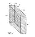
- FIG. 4is a block diagram of a fourth embodiment.
- a computer 10includes a metal or plastic chassis 12 in which a motherboard 14 is mounted.
- a chassisis the physical frame or structure of a computer that houses the main electronic components, including the motherboard 14 with places (not shown) to insert or replace microchips for the main and possibly specialized processors and random access memory (RAM) and places for adding optional adapters like audio or video capabilities, for example. Typically, room is also provided for a hard-disk drive and a CD-ROM drive.
- a processor 16is connected to the motherboard 14 .
- a number of memory devices or modules 18 and two input/output (I/O) devices 20are also mounted to the motherboard 14 .
- Two buses 16 a and 16 bare also provided on the motherboard 14 and connect the processor 16 to the memory modules 18 and to the input/output devices 20 , respectively.
- a power supply 22is connected to the motherboard 14 and a pair of cable assemblies 24 a and 24 b connect the motherboard 14 to a hard drive unit 26 and a disk drive 28 .
- Other components(not shown), electrical traces, electrical circuits and related devices may also be provided in the chassis 12 .
- a layer 30 of electromagnetic interference (EMI) emission absorption materialis covered with a layer 30 of electromagnetic interference (EMI) emission absorption material.
- the layer 30is affixed to the interior walls of chassis 12 and absorbs electromagnetic emissions.
- the layer 30can absorb 6 dB of the EMI emission.
- the layer 30can protect sensitive components in a wireless device from emissions from circuitry or transmitting antenna. Rather than containing EMI emissions, the layer 30 absorbs the EMI emissions.
- One or more layers of EMI emission absorption materialscan easily be applied to all computer-type systems, such as work stations, desktop computers, servers, as well as any electronic device, such as personal data assistants (PDAs), wireless devices, internet tables, game consoles and peripherals.
- PDAspersonal data assistants
- the layer 30is shown attached to an interior of a side panel 32 of the chassis 12 .
- An adhesiveis used to bond the layer 30 to the side panel 32 during manufacturing and assembly of the chassis 12 and sized to the dimensions of the interior portion of the side panel 32 of the chassis 12 .
- No electrical groundingis required.
- the layer 30may be fabricated in a variety of thicknesses to cover a wide range of EMI emission ranges.
- the layer 30may be constructed as a lightweight, flexible, low density, and high-loss foam. Thickness may range, for example, from 0.01′′ to 1.0′′, and densities may range, for example, from 0.05 to 5.0 pounds per cubic foot, however the thickness and densities are not limited to these values.
- the layer 30may be single layer, multilayer, weatherproof, reticulated and or rigid. Suitable EMI emission absorber material is supplied, for example, by R+F Products of San Marcos, Calif. and ARC Technologies of Amesbury, Mass.
- the chassis 12may be fitted with a molded, i.e., rigid, EMI emission absorption panel 34 that replaces a metal or plastic panel of FIG. 1 .
- the panel 34is, for example, a reticulated foam with a continuously graded lossy coating produced using a two part closed cell polyurethane filler to provide structural integrity.
- the front panel 34replaces the front wall of the chassis with a rigid material capable of EMI emission absorption.
- the chassis 12includes a front panel 40 of rigid EMI absorption material and two side panels 42 a, 42 b of rigid EMI absorption material.
- a back panel 44has attached on an interior surface 46 a panel 48 of flexible EMI absorption material.
- one or more of the interior and/or exterior metal or plastic walls of the chassis 12are replaced with solid molded EMI emission absorption panels.
- Use of the molded EMI emission absorption panelsalso provides thermal venting since it is porous and not impermeable. Further, combining a different EMI emission absorption material in a single panel or layer covers a very wide frequency band.
- layers of EMI emission absorption materialsare used to line internal bays within the chassis, like, for example, a bay in which the power supply 22 resides.
- EMI emission absorption materialsare used to suppress EMI around slots in computer peripherals, such as CD-ROMs, DVDs, CD-RWs and floppy/disk drives.
Landscapes
- Shielding Devices Or Components To Electric Or Magnetic Fields (AREA)
Abstract
Description
This invention relates to reducing electromagnetic interference (EMI) emissions.
During the operation of computers, or other similar electronic components, electromagnetic interference (EMI) emissions, or radiation, are generated by motors, drives, processors, chips and circuits. One way to contain these emissions is to surround the circuit in a metal panel. Further, in some situations, these emissions must be contained in order to comply with certain regulations.
FIG. 1 is a block diagram of a first embodiment.
FIG. 2 is a block diagram of a second embodiment.
FIG. 3 is a block diagram of a third embodiment.
FIG. 4 is a block diagram of a fourth embodiment.
Referring to FIG. 1, acomputer 10 includes a metal orplastic chassis 12 in which amotherboard 14 is mounted. A chassis is the physical frame or structure of a computer that houses the main electronic components, including themotherboard 14 with places (not shown) to insert or replace microchips for the main and possibly specialized processors and random access memory (RAM) and places for adding optional adapters like audio or video capabilities, for example. Typically, room is also provided for a hard-disk drive and a CD-ROM drive. Aprocessor 16 is connected to themotherboard 14. A number of memory devices ormodules 18 and two input/output (I/O)devices 20 are also mounted to themotherboard 14. Twobuses motherboard 14 and connect theprocessor 16 to thememory modules 18 and to the input/output devices 20, respectively. Apower supply 22 is connected to themotherboard 14 and a pair ofcable assemblies motherboard 14 to ahard drive unit 26 and adisk drive 28. Other components (not shown), electrical traces, electrical circuits and related devices may also be provided in thechassis 12.
At least part of the interior walls of thechassis 12 is covered with alayer 30 of electromagnetic interference (EMI) emission absorption material. Thelayer 30 is affixed to the interior walls ofchassis 12 and absorbs electromagnetic emissions. For example, in a personal computer where thechassis 12 may be expected to provide 6 dB attenuation of EMI emission, thelayer 30 can absorb 6 dB of the EMI emission. In another example, thelayer 30 can protect sensitive components in a wireless device from emissions from circuitry or transmitting antenna. Rather than containing EMI emissions, thelayer 30 absorbs the EMI emissions. One or more layers of EMI emission absorption materials can easily be applied to all computer-type systems, such as work stations, desktop computers, servers, as well as any electronic device, such as personal data assistants (PDAs), wireless devices, internet tables, game consoles and peripherals.
Referring to FIG. 2, thelayer 30 is shown attached to an interior of aside panel 32 of thechassis 12. An adhesive is used to bond thelayer 30 to theside panel 32 during manufacturing and assembly of thechassis 12 and sized to the dimensions of the interior portion of theside panel 32 of thechassis 12. No electrical grounding is required. Thelayer 30 may be fabricated in a variety of thicknesses to cover a wide range of EMI emission ranges. For example, thelayer 30 may be constructed as a lightweight, flexible, low density, and high-loss foam. Thickness may range, for example, from 0.01″ to 1.0″, and densities may range, for example, from 0.05 to 5.0 pounds per cubic foot, however the thickness and densities are not limited to these values. Thelayer 30 may be single layer, multilayer, weatherproof, reticulated and or rigid. Suitable EMI emission absorber material is supplied, for example, by R+F Products of San Marcos, Calif. and ARC Technologies of Amesbury, Mass.
Referring to FIG. 3, in another approach, thechassis 12 may be fitted with a molded, i.e., rigid, EMIemission absorption panel 34 that replaces a metal or plastic panel of FIG.1. Thepanel 34 is, for example, a reticulated foam with a continuously graded lossy coating produced using a two part closed cell polyurethane filler to provide structural integrity. Thus, rather than bonding alayer 30 to the interior walls of thechassis 12, thefront panel 34 replaces the front wall of the chassis with a rigid material capable of EMI emission absorption.
Referring to FIG. 4, in still another approach, thechassis 12 includes afront panel 40 of rigid EMI absorption material and twoside panels back panel 44 has attached on an interior surface46 apanel 48 of flexible EMI absorption material.
In other examples, one or more of the interior and/or exterior metal or plastic walls of thechassis 12 are replaced with solid molded EMI emission absorption panels. Use of the molded EMI emission absorption panels also provides thermal venting since it is porous and not impermeable. Further, combining a different EMI emission absorption material in a single panel or layer covers a very wide frequency band.
In still other examples, layers of EMI emission absorption materials are used to line internal bays within the chassis, like, for example, a bay in which thepower supply 22 resides.
In another example, where slots are common in computer peripherals for assembly and thermal reasons, radiation from these slots may cause EMI problems. Layers of EMI emission absorption materials are used to suppress EMI around slots in computer peripherals, such as CD-ROMs, DVDs, CD-RWs and floppy/disk drives.
Other embodiments are within the following claims.
Claims (26)
1. A system comprising:
a chassis having at least one wall, the chassis housing electrical components; and a layer of flexible, lightweight, low density, high-loss foam electromagnetic interference (EMI) emission absorption material covering an interior surface of the wall, the material having a thickness of 0.01″ to 1.0″ and a density of 0.05 to 5 pounds per cubic foot.
2. The system ofclaim 1 wherein the layer comprises a single layer of lossy foam.
3. The system ofclaim 1 wherein the layer comprises multiple layers of lossy foam.
4. The system ofclaim 1 wherein the layer comprises a layer of weatherproof lossy foam.
5. The system ofclaim 1 in which the layer covers all walls within the chassis.
6. The system ofclaim 1 in which the layer covers more than one wall within the chassis.
7. The system ofclaim 1 in which another wall is made entirely of a rigid EMI emission absorption material.
8. Apparatus comprising:
an electrical chassis, at least one rigid reticulated foam with a continuously graded lossy coating produced using a two part closed cell polyurethane filler connected to a plurality of non-shielded walls.
9. Apparatus comprising:
panels joined to form a chassis;
at least one bay located within an interior of the chassis, the bay having at least one wall; and
a layer of flexible, lightweight, low density, high-loss foam EMI emission absorption material affixed to an interior surface of the wall of the bay, the material having a thickness of 0.01″ to 1.0″ and a density of 0.05 to 5 Pounds per cubic foot.
10. The apparatus ofclaim 9 in which a second wall is constructed from a rigid foam EMI emission absorption material.
11. An enclosure comprising:
a front panel constructed from a rigid reticulated foam with a continuously graded lossy coating produced using a two part closed cell polyurethane filler and joined to two side panels, an upper panel and a lower panel; and
a rear panel joined to the two side panels and upper and lower panels.
12. The enclosure ofclaim 11 in which the two side panels are constructed of a rigid reticulated foam EMI emission absorption material.
13. The enclosure ofclaim 11 in which the upper and lower panels are constructed of a rigid reticulated foam EMI emission absorption material.
14. The enclosure ofclaim 11 further comprising internal bays having walls lined with a flexible foam EMI emission absorption material.
15. The enclosure ofclaim 11 further comprising internal bays having walls constructed of a rigid reticulated foam EMI emission absorption material.
16. A method comprising:
forming a front panel from a rigid reticulated foam with a continuously graded lossy coating produced using a two part closed cell polyurethane filler; and
joining the front panel to a top and bottom panel, two side panels and a back panel.
17. The method ofclaim 16 further comprising:
providing internal bays having metal walls; and
covering the metal walls with a first layer of flexible foam EMI emission absorption material.
18. The method ofclaim 17 further comprising covering the metal walls with a second layer of foam EMI emission absorber material.
19. The method ofclaim 16 further comprising covering an interior side of the top and bottom wall with a flexible foam EMI emission absorption material.
20. The method ofclaim 16 further comprising covering an interior surface of the back panel with a flexible foam EMI emission absorption material.
21. The method ofclaim 16 further comprising covering an interior surface of the two side panels with a flexible foam EMI emission absorption material.
22. A system comprising:
a chassis containing a plurality of slots, the chassis housing electrical components; and
a layer of flexible, lightweight, low density, high-loss foam electromagnetic interference (EMI) emission absorption material covering at least one of the slots, the material having a thickness of 0.01″ to 1.0″ and a density of 0.05 to 5 pounds per cubic foot.
23. The system ofclaim 22 wherein the layer comprises a single layer of lossy foam.
24. The system ofclaim 22 wherein the layer comprises multiple layers of lossy foam.
25. The system ofclaim 22 wherein the layer comprises a layer of weatherproof lossy foam.
26. The system ofclaim 22 in which the layer covers more than one slot.
Priority Applications (1)
| Application Number | Priority Date | Filing Date | Title |
|---|---|---|---|
| US10/017,456US6672902B2 (en) | 2001-12-12 | 2001-12-12 | Reducing electromagnetic interference (EMI) emissions |
Applications Claiming Priority (1)
| Application Number | Priority Date | Filing Date | Title |
|---|---|---|---|
| US10/017,456US6672902B2 (en) | 2001-12-12 | 2001-12-12 | Reducing electromagnetic interference (EMI) emissions |
Publications (2)
| Publication Number | Publication Date |
|---|---|
| US20030109175A1 US20030109175A1 (en) | 2003-06-12 |
| US6672902B2true US6672902B2 (en) | 2004-01-06 |
Family
ID=21782683
Family Applications (1)
| Application Number | Title | Priority Date | Filing Date |
|---|---|---|---|
| US10/017,456Expired - LifetimeUS6672902B2 (en) | 2001-12-12 | 2001-12-12 | Reducing electromagnetic interference (EMI) emissions |
Country Status (1)
| Country | Link |
|---|---|
| US (1) | US6672902B2 (en) |
Cited By (12)
| Publication number | Priority date | Publication date | Assignee | Title |
|---|---|---|---|---|
| US20040165347A1 (en)* | 2003-02-24 | 2004-08-26 | Roesner Arlen L. | Computer identification system and method |
| US20050281003A1 (en)* | 2004-06-21 | 2005-12-22 | Carullo Thomas J | Waveguide power supply enclosure |
| US20060285851A1 (en)* | 2005-06-16 | 2006-12-21 | Jiaxi Kan | Optical transceivers and methods to reduce interference in optical transceivers |
| US20070145595A1 (en)* | 2005-12-27 | 2007-06-28 | Hall Stephen H | High speed interconnect |
| US20080157903A1 (en)* | 2006-12-29 | 2008-07-03 | Hall Stephen H | Ultra-high bandwidth interconnect for data transmission |
| US20090147455A1 (en)* | 2007-12-11 | 2009-06-11 | Dell Products, Lp | Information handling systems having coatings with porous particles and processes of forming the same |
| US7976340B1 (en)* | 2010-03-12 | 2011-07-12 | Tyco Electronics Corporation | Connector system with electromagnetic interference shielding |
| US20120001001A1 (en)* | 2009-10-05 | 2012-01-05 | Hermann Schwelling | File shredder having a metal detector |
| US8742267B2 (en)* | 2012-05-29 | 2014-06-03 | Hong Fu Jin Precision Industry (Shenzhen) Co., Ltd. | Electromagnetic interference shielding assembly and electronic device having same |
| US20150333452A1 (en)* | 2014-05-14 | 2015-11-19 | Commscope Technologies Llc | Rf-isolating sealing enclosure and interconnection junctions protected thereby |
| US20170132168A1 (en)* | 2015-11-09 | 2017-05-11 | Dell Products, Lp | System and Method for Providing Wireless Communications to a Boxed Server |
| US9731456B2 (en) | 2013-03-14 | 2017-08-15 | Sabic Global Technologies B.V. | Method of manufacturing a functionally graded article |
Families Citing this family (4)
| Publication number | Priority date | Publication date | Assignee | Title |
|---|---|---|---|---|
| US7138896B2 (en) | 2004-06-29 | 2006-11-21 | International Business Machines Corporation | Ferrite core, and flexible assembly of ferrite cores for suppressing electromagnetic interference |
| US8018725B2 (en)* | 2007-06-07 | 2011-09-13 | Tyco Electronics Corporation | Cable support bracket for an electrical component |
| GB201412572D0 (en)* | 2014-07-15 | 2014-08-27 | Univ Bristol | Wireless sensor |
| US20230127240A1 (en)* | 2021-10-22 | 2023-04-27 | EMC IP Holding Company, LLC | Chassis Node Coupling System |
Citations (24)
| Publication number | Priority date | Publication date | Assignee | Title |
|---|---|---|---|---|
| US4404617A (en)* | 1978-08-07 | 1983-09-13 | Sadahiro Ohyama | High-frequency circuit device having a circuit board fixed to a shield casing by projections of the shield casing and soldering |
| US4717990A (en)* | 1986-05-30 | 1988-01-05 | Motorola, Inc. | Double-shielded housing for RF circuitry |
| US4931479A (en)* | 1988-11-07 | 1990-06-05 | Chomerics, Inc. | Foam in place conductive polyurethane foam |
| US4964017A (en)* | 1989-04-26 | 1990-10-16 | Intelligent Instrumentation, Inc. | Adaptable housing for embedding of computer-controlled products |
| US5155316A (en)* | 1990-12-24 | 1992-10-13 | Chiu Sou Kuein | Heat-conducting mat for absorbing microwave and electromagnetic wave energy |
| US5244708A (en)* | 1990-03-28 | 1993-09-14 | Fujita Corporation | Electromagnetic wave shielding interior material |
| US5278351A (en)* | 1991-04-02 | 1994-01-11 | Zeos International, Inc. | Personal computer cabinet cover with EMI clips |
| US5473110A (en)* | 1995-03-07 | 1995-12-05 | Unisys Corporation | Magnetically-attachable EMI shielding cover for attenuating electromagnetic emanation |
| US5562497A (en)* | 1994-05-25 | 1996-10-08 | Molex Incorporated | Shielded plug assembly |
| US5583318A (en)* | 1993-12-30 | 1996-12-10 | Lucent Technologies Inc. | Multi-layer shield for absorption of electromagnetic energy |
| US5676812A (en)* | 1990-03-24 | 1997-10-14 | Canon Kabushiki Kaisha | Electronic equipment with an adhesive member to intercept electromagnetic waves |
| US6018125A (en)* | 1996-11-15 | 2000-01-25 | Collins; Pat Eliot | High frequency EMI shield with air flow for electronic device enclosure |
| US6046652A (en)* | 1997-03-31 | 2000-04-04 | International Business Machines Corporation | Loading element for EMI prevention within an enclosure |
| US6114622A (en)* | 1998-05-06 | 2000-09-05 | Bermo, Inc. | Personal computer chassis with hinged side wall |
| US6137694A (en)* | 1998-10-19 | 2000-10-24 | International Business Machines Corporation | Integral EMI shielding for computer enclosures |
| US6140577A (en)* | 1998-10-08 | 2000-10-31 | Gateway 2000, Inc | Electronic chassis electro-magnetic interference seal and sealing device |
| US6242691B1 (en)* | 1999-02-03 | 2001-06-05 | Lockheed Martin Corporation | Electronic packaging and method of packaging |
| US6278606B1 (en)* | 1999-01-06 | 2001-08-21 | Dell Usa, L.P. | Computer and method for EMI containment in a computer |
| US6309742B1 (en)* | 2000-01-28 | 2001-10-30 | Gore Enterprise Holdings, Inc. | EMI/RFI shielding gasket |
| US6346491B1 (en)* | 1999-05-28 | 2002-02-12 | Milliken & Company | Felt having conductivity gradient |
| US6359213B1 (en)* | 1999-10-26 | 2002-03-19 | L. Jacqueline Long | Emissions blocking apparatus |
| US20020046849A1 (en)* | 2000-01-24 | 2002-04-25 | Rapp Martin L. | Methods and apparatus for EMI shielding |
| US6410847B1 (en)* | 2000-07-25 | 2002-06-25 | Trw Inc. | Packaged electronic system having selectively plated microwave absorbing cover |
| US20020104670A1 (en)* | 2001-02-06 | 2002-08-08 | Richard Marmel | Magnetic insulation for electronic devices |
- 2001
- 2001-12-12USUS10/017,456patent/US6672902B2/ennot_activeExpired - Lifetime
Patent Citations (25)
| Publication number | Priority date | Publication date | Assignee | Title |
|---|---|---|---|---|
| US4404617A (en)* | 1978-08-07 | 1983-09-13 | Sadahiro Ohyama | High-frequency circuit device having a circuit board fixed to a shield casing by projections of the shield casing and soldering |
| US4717990A (en)* | 1986-05-30 | 1988-01-05 | Motorola, Inc. | Double-shielded housing for RF circuitry |
| US4931479A (en)* | 1988-11-07 | 1990-06-05 | Chomerics, Inc. | Foam in place conductive polyurethane foam |
| US4931479B1 (en)* | 1988-11-07 | 2000-10-10 | Parker Intangibles Inc | Foam in place conductive polyurethane foam |
| US4964017A (en)* | 1989-04-26 | 1990-10-16 | Intelligent Instrumentation, Inc. | Adaptable housing for embedding of computer-controlled products |
| US5676812A (en)* | 1990-03-24 | 1997-10-14 | Canon Kabushiki Kaisha | Electronic equipment with an adhesive member to intercept electromagnetic waves |
| US5244708A (en)* | 1990-03-28 | 1993-09-14 | Fujita Corporation | Electromagnetic wave shielding interior material |
| US5155316A (en)* | 1990-12-24 | 1992-10-13 | Chiu Sou Kuein | Heat-conducting mat for absorbing microwave and electromagnetic wave energy |
| US5278351A (en)* | 1991-04-02 | 1994-01-11 | Zeos International, Inc. | Personal computer cabinet cover with EMI clips |
| US5583318A (en)* | 1993-12-30 | 1996-12-10 | Lucent Technologies Inc. | Multi-layer shield for absorption of electromagnetic energy |
| US5562497A (en)* | 1994-05-25 | 1996-10-08 | Molex Incorporated | Shielded plug assembly |
| US5473110A (en)* | 1995-03-07 | 1995-12-05 | Unisys Corporation | Magnetically-attachable EMI shielding cover for attenuating electromagnetic emanation |
| US6018125A (en)* | 1996-11-15 | 2000-01-25 | Collins; Pat Eliot | High frequency EMI shield with air flow for electronic device enclosure |
| US6046652A (en)* | 1997-03-31 | 2000-04-04 | International Business Machines Corporation | Loading element for EMI prevention within an enclosure |
| US6114622A (en)* | 1998-05-06 | 2000-09-05 | Bermo, Inc. | Personal computer chassis with hinged side wall |
| US6140577A (en)* | 1998-10-08 | 2000-10-31 | Gateway 2000, Inc | Electronic chassis electro-magnetic interference seal and sealing device |
| US6137694A (en)* | 1998-10-19 | 2000-10-24 | International Business Machines Corporation | Integral EMI shielding for computer enclosures |
| US6278606B1 (en)* | 1999-01-06 | 2001-08-21 | Dell Usa, L.P. | Computer and method for EMI containment in a computer |
| US6242691B1 (en)* | 1999-02-03 | 2001-06-05 | Lockheed Martin Corporation | Electronic packaging and method of packaging |
| US6346491B1 (en)* | 1999-05-28 | 2002-02-12 | Milliken & Company | Felt having conductivity gradient |
| US6359213B1 (en)* | 1999-10-26 | 2002-03-19 | L. Jacqueline Long | Emissions blocking apparatus |
| US20020046849A1 (en)* | 2000-01-24 | 2002-04-25 | Rapp Martin L. | Methods and apparatus for EMI shielding |
| US6309742B1 (en)* | 2000-01-28 | 2001-10-30 | Gore Enterprise Holdings, Inc. | EMI/RFI shielding gasket |
| US6410847B1 (en)* | 2000-07-25 | 2002-06-25 | Trw Inc. | Packaged electronic system having selectively plated microwave absorbing cover |
| US20020104670A1 (en)* | 2001-02-06 | 2002-08-08 | Richard Marmel | Magnetic insulation for electronic devices |
Cited By (19)
| Publication number | Priority date | Publication date | Assignee | Title |
|---|---|---|---|---|
| US20040165347A1 (en)* | 2003-02-24 | 2004-08-26 | Roesner Arlen L. | Computer identification system and method |
| US20050281003A1 (en)* | 2004-06-21 | 2005-12-22 | Carullo Thomas J | Waveguide power supply enclosure |
| US20060285851A1 (en)* | 2005-06-16 | 2006-12-21 | Jiaxi Kan | Optical transceivers and methods to reduce interference in optical transceivers |
| US20070145595A1 (en)* | 2005-12-27 | 2007-06-28 | Hall Stephen H | High speed interconnect |
| US8732942B2 (en) | 2005-12-27 | 2014-05-27 | Intel Corporation | Method of forming a high speed interconnect |
| US20080172872A1 (en)* | 2005-12-27 | 2008-07-24 | Intel Corporation | High speed interconnect |
| US7800459B2 (en) | 2006-12-29 | 2010-09-21 | Intel Corporation | Ultra-high bandwidth interconnect for data transmission |
| US20080157903A1 (en)* | 2006-12-29 | 2008-07-03 | Hall Stephen H | Ultra-high bandwidth interconnect for data transmission |
| US7729108B2 (en)* | 2007-12-11 | 2010-06-01 | Dell Products, Lp | Information handling systems having coatings with porous particles and processes of forming the same |
| US20090147455A1 (en)* | 2007-12-11 | 2009-06-11 | Dell Products, Lp | Information handling systems having coatings with porous particles and processes of forming the same |
| US20120001001A1 (en)* | 2009-10-05 | 2012-01-05 | Hermann Schwelling | File shredder having a metal detector |
| US9254491B2 (en)* | 2009-10-05 | 2016-02-09 | Hermann Schwelling | File shredder having a metal detector |
| US7976340B1 (en)* | 2010-03-12 | 2011-07-12 | Tyco Electronics Corporation | Connector system with electromagnetic interference shielding |
| US8742267B2 (en)* | 2012-05-29 | 2014-06-03 | Hong Fu Jin Precision Industry (Shenzhen) Co., Ltd. | Electromagnetic interference shielding assembly and electronic device having same |
| US9731456B2 (en) | 2013-03-14 | 2017-08-15 | Sabic Global Technologies B.V. | Method of manufacturing a functionally graded article |
| US20150333452A1 (en)* | 2014-05-14 | 2015-11-19 | Commscope Technologies Llc | Rf-isolating sealing enclosure and interconnection junctions protected thereby |
| US9653852B2 (en)* | 2014-05-14 | 2017-05-16 | Commscope Technologies Llc | RF-isolating sealing enclosure and interconnection junctions protected thereby |
| US20170132168A1 (en)* | 2015-11-09 | 2017-05-11 | Dell Products, Lp | System and Method for Providing Wireless Communications to a Boxed Server |
| US10229082B2 (en)* | 2015-11-09 | 2019-03-12 | Dell Products, Lp | System and method for providing wireless communications to a boxed server |
Also Published As
| Publication number | Publication date |
|---|---|
| US20030109175A1 (en) | 2003-06-12 |
Similar Documents
| Publication | Publication Date | Title |
|---|---|---|
| US6672902B2 (en) | Reducing electromagnetic interference (EMI) emissions | |
| US6671186B2 (en) | Electromagnetic interference shield | |
| US6122167A (en) | Integrated hybrid cooling with EMI shielding for a portable computer | |
| US5353202A (en) | Personal computer with shielding of input/output signals | |
| US5570270A (en) | Chassis and personal computer for severe environment embedded applications | |
| US5473507A (en) | Chassis of a device | |
| US6542384B1 (en) | Riser card local EMI shield for a computer chassis | |
| AU2016222502B9 (en) | Architecture features of an electronic device | |
| US8411432B1 (en) | System, apparatus and method for tiered shock solution | |
| US5713790A (en) | Embedded heat dissipating device mounting structure | |
| US20080192425A1 (en) | Thin Solid State Drive Housing Structures | |
| US6362968B1 (en) | Computer system motherboard stiffener | |
| US20020057813A1 (en) | Impact-resistant electronic device | |
| MY110236A (en) | Personal computer enclosure with shielding. | |
| JP2003133448A (en) | Apparatus and method for shielding device | |
| JP2001160663A (en) | Circuit substrate | |
| US6538903B1 (en) | Method and apparatus for reducing electromagnetic radiation from a computer enclosure | |
| US6208516B1 (en) | Electromagnetic interference shield and gap filler for a circuit board | |
| JP2006173609A (en) | Electronic system and method for configuring electronic system for reducing electromagnetic interference | |
| US6274807B1 (en) | Method and apparatus for controlling electromagnetic radiation emissions generated by electrical components | |
| JP2005268428A (en) | PCB electromagnetic shield structure | |
| JP2009212187A (en) | Electronic control device | |
| US6723915B2 (en) | Emi-shielding riser card for a computer chassis | |
| JPH08125373A (en) | Electronics | |
| US20010053677A1 (en) | Method and apparatus for integrating an intentional radiator in a system |
Legal Events
| Date | Code | Title | Description |
|---|---|---|---|
| AS | Assignment | Owner name:INTEL CORPORATION, CALIFORNIA Free format text:ASSIGNMENT OF ASSIGNORS INTEREST;ASSIGNORS:HECK, HOWARD L.;CHANG, STEVE Y.;SKINNER, HARRY G.;AND OTHERS;REEL/FRAME:012953/0977;SIGNING DATES FROM 20020516 TO 20020520 | |
| STCF | Information on status: patent grant | Free format text:PATENTED CASE | |
| FEPP | Fee payment procedure | Free format text:PAYER NUMBER DE-ASSIGNED (ORIGINAL EVENT CODE: RMPN); ENTITY STATUS OF PATENT OWNER: LARGE ENTITY Free format text:PAYOR NUMBER ASSIGNED (ORIGINAL EVENT CODE: ASPN); ENTITY STATUS OF PATENT OWNER: LARGE ENTITY | |
| FPAY | Fee payment | Year of fee payment:4 | |
| FPAY | Fee payment | Year of fee payment:8 | |
| FPAY | Fee payment | Year of fee payment:12 |