US6670921B2 - Low-cost HDMI-D packaging technique for integrating an efficient reconfigurable antenna array with RF MEMS switches and a high impedance surface - Google Patents
Low-cost HDMI-D packaging technique for integrating an efficient reconfigurable antenna array with RF MEMS switches and a high impedance surfaceDownload PDFInfo
- Publication number
- US6670921B2 US6670921B2US09/906,035US90603501AUS6670921B2US 6670921 B2US6670921 B2US 6670921B2US 90603501 AUS90603501 AUS 90603501AUS 6670921 B2US6670921 B2US 6670921B2
- Authority
- US
- United States
- Prior art keywords
- layer
- array
- switches
- metallic
- patterned
- Prior art date
- Legal status (The legal status is an assumption and is not a legal conclusion. Google has not performed a legal analysis and makes no representation as to the accuracy of the status listed.)
- Expired - Lifetime
Links
Images
Classifications
- H—ELECTRICITY
- H01—ELECTRIC ELEMENTS
- H01P—WAVEGUIDES; RESONATORS, LINES, OR OTHER DEVICES OF THE WAVEGUIDE TYPE
- H01P1/00—Auxiliary devices
- H01P1/20—Frequency-selective devices, e.g. filters
- H01P1/2005—Electromagnetic photonic bandgaps [EPB], or photonic bandgaps [PBG]
- H—ELECTRICITY
- H01—ELECTRIC ELEMENTS
- H01Q—ANTENNAS, i.e. RADIO AERIALS
- H01Q1/00—Details of, or arrangements associated with, antennas
- H01Q1/36—Structural form of radiating elements, e.g. cone, spiral, umbrella; Particular materials used therewith
- H01Q1/38—Structural form of radiating elements, e.g. cone, spiral, umbrella; Particular materials used therewith formed by a conductive layer on an insulating support
- H—ELECTRICITY
- H01—ELECTRIC ELEMENTS
- H01Q—ANTENNAS, i.e. RADIO AERIALS
- H01Q15/00—Devices for reflection, refraction, diffraction or polarisation of waves radiated from an antenna, e.g. quasi-optical devices
- H01Q15/0006—Devices acting selectively as reflecting surface, as diffracting or as refracting device, e.g. frequency filtering or angular spatial filtering devices
- H01Q15/006—Selective devices having photonic band gap materials or materials of which the material properties are frequency dependent, e.g. perforated substrates, high-impedance surfaces
- H01Q15/0066—Selective devices having photonic band gap materials or materials of which the material properties are frequency dependent, e.g. perforated substrates, high-impedance surfaces said selective devices being reconfigurable, tunable or controllable, e.g. using switches
- H—ELECTRICITY
- H01—ELECTRIC ELEMENTS
- H01Q—ANTENNAS, i.e. RADIO AERIALS
- H01Q15/00—Devices for reflection, refraction, diffraction or polarisation of waves radiated from an antenna, e.g. quasi-optical devices
- H01Q15/0006—Devices acting selectively as reflecting surface, as diffracting or as refracting device, e.g. frequency filtering or angular spatial filtering devices
- H01Q15/006—Selective devices having photonic band gap materials or materials of which the material properties are frequency dependent, e.g. perforated substrates, high-impedance surfaces
- H01Q15/008—Selective devices having photonic band gap materials or materials of which the material properties are frequency dependent, e.g. perforated substrates, high-impedance surfaces said selective devices having Sievenpipers' mushroom elements
Definitions
- This inventionrelates to a low-cost packaging method which utilizes a commercially available High Density Multilayer Interconnect (HDMI or sometimes simply HDI) package and multichip interconnect for the integration of a novel 2-D reconfigurable antenna array with Radio Frequency (RF) Microelectromechanical (MEM) switches on top of a high impedance surface (High-Z Surface).
- HDMIHigh Density Multilayer Interconnect
- RFRadio Frequency
- MEMMicroelectromechanical
- the prior artalso includes RF MEMS tunable dipoles 1 ⁇ 4 wavelength above a metallic ground plane, but this approach results in limited bandwidth and is not suspectible to convenient packaging.
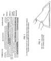
- FIG. 1illustrates a cross-section of a prior art thin film copper/polyimide multilayer HDMI MCM-D integrated structure fabricated on a silicon substrate.
- the fabrication processinvolves spin or curtain coating of ⁇ 10- ⁇ m-thick polyimide dielectric layers and sputter deposition of ⁇ 10- ⁇ m-thick copper conductor layers in an interactive process which includes phase mask laser formation of z-axis interconnect vias and metal patterning.
- more than 35,000 complex 2′′ ⁇ 4′′ MCM-D moduleshave been built and used in airborne radar, military and commercial satellites, and space projectiles to meet demanding weight and volume requirements, with no reported field failures.
- the substrate for this package used in the present inventionis preferably either glass, quartz or silicon (Si).
- a Hi-Zis also provided.
- the dielectric for the Hi-Z surfaceis a polyimide layer which may have been originally used for the packaging.
- the antennais placed adjacent the Hi-Z surface, and the RF MEMS switches are used to reconfigure the antenna simply by changing the dipole's length.
- the feed structures for the antennas and dc linesare placed behind the Hi-Z Surface, so that they do not interfere with the radiation pattern of the antenna. The whole package is environmentally protected.
- the Hi-Z surface utilizedis a Hi-Z surface with added discrete inductors.
- RF MEMS switchesoffer very low insertion loss ( ⁇ 0.2 dB) and high isolation (>35 dB) over a very broad frequency range from dc to 40 GHz. Furthermore, they consume very little power (i.e. less than 200 pJ per activation). The High-Z Surface allows the antenna to be very compact. Finally, since the antenna is reconfigurable by means of the RF MEM switches, it can be made to operate at different desired frequencies.
- the present inventionprovides, in one aspect thereof, a method of making a thin, flexible antenna.
- a layer of a flexible insulating mediumis deposited on a substrate and patterning the layer of insulating medium to form openings therein.
- metal layersare deposited on a previously deposited insulating layer and patterned as needed and layers of a flexible insulating medium are deposited on the previously deposited metal layer and patterned as needed, the layers of metal and layers of insulating medium forming form a multilayered high impedance surface having an upper surface with antenna segments having been patterned from a metal layer previously deposited thereat, an array of metallic top elements formed in a layer spaced from the upper surface, the array of metallic top elements having been patterned from a metal layer previously deposited thereat, a metallic ground plane formed in a layer spaced from the array of metallic top elements, the metallic ground plane having been formed from a metal layer previously deposited thereat, and inductive elements coupling each of the top elements in the array of metallic top elements with the ground plane, the inductive elements having been formed from one or more metal layers previously deposited.
- optically controlled switchesare disposed adjacent at least selected ones of the antenna segments for coupling the adjacent antenna segments together in response to light impinging a photovoltaic cell associated each optically controlled switch.
- Optic fibersare arranged on or adjacent the high impedance surface with distal ends of each optic fiber being coupled to a respective one of the optically controlled switches for coupling light carried by the optic fibre to the photovoltaic cells associated with the optically controlled switch.
- the multilayered high impedance surface from the substrate, the substratesimply providing a support for making the thin, flexible antenna during manufacture.
- FIG. 1is a cross sectional view through a thin film copper/polyimide multilayer HDMI MCM-D integration structure fabricated upon a silicon substrate;
- FIG. 2depicts a HDMI decal being peeled from a reuseable quartz carrier or substrate
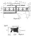
- FIG. 3 ais a cross sectional view of an HDMI reconfigurable antenna in accordance with the present invention.
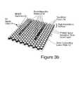
- FIG. 3 bis a perspective view of the HDMI reconfigurable antenna of FIG. 3 a , with the polyimide layers and the dielectric top layer omitted for clarity's sake;
- FIG. 4is a top view of an optically controlled MEMS switch.
- FIG. 2shows a 24′′ ⁇ 24′′0.007′′-thick flexible multi-layer HDMI interconnection structure being removed from the reusable carrier upon which it was fabricated.
- FIG. 3 ashows a cross-section the reconfigurable antenna of the present invention.
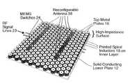
- the first 1 , second 2 , and third 3 HDMI layersare utilized to help define a Hi-Z surface 10 and preferably a Hi-Z surface with added discrete inductors 18 .
- Plated through metallic viasform a plurality of pairs of studs 14 a , 14 b , each pair connecting each metallic top element 16 of Hi-Z surface formed on the third layer 3 to a ground plane 12 formed on the first layer 1 .
- a plurality of discrete inductors 18are optionally formed on the third layer with each inductor 28 of the plurality being arranged in series with each pair of studs 14 a , 14 b to increase the bandwidth of the Hi-Z surface.
- those practicing the present inventionmay decide not to use discrete inductors 18 , in which case layers 2 and 3 can then be combined into a single layer and the plurality of pairs of studs 14 a , 14 b would typically then be replaced by a plurality of single studs.
- the top elements 16are closely arranged to capacitively couple them to neighboring elements 16 .
- antenna dipole segments 22 and RF MEMS switches 24are disposed above the Hi-Z surface formed on layers 1 - 3 .
- the antenna dipole elements 22are preferably formed on a layer 1 which overlays the Hi-Z surface formed on layers 1 - 3 .
- the antenna dipole segment feed lines 23are preferably arranged beneath the ground plane 12 on layer 4 and are connected by studs 25 formed by metal filled via holes through layers 1 - 4 to the dipole segments 22 .
- the RF MEM switches 24are preferably optically controlled. Optically controlled RF MEMS switches 24 are equipped with photovoltaic cells 16 (FIG. 4) which provide an actuation voltage for an associated cantilevered arm 28 (FIG. 4 ).
- FIG. 3 bis a perspective view of the HDMI reconfigurable antenna of FIG. 3 a , with the polyimide layers 1 , 2 , 3 , and 4 and the dielectric top layer 36 omitted for clarity's sake.
- the top elements 16are shown in a two dimensional array disposed over the ground plane 12 .
- Each top elementhas an associated discrete inductor 18 in this embodiment.
- the discrete inductors 18may be omitted since there may be sufficient inductive inherent in the other structures depicted. In that case, one of the mid layers 2 or 3 may also be omitted.
- the inductors 18are depicted in FIG. 3 a are preferably coil-shaped inductors.
- the top elements 16are depicted as being hexagonal in plan view (see FIG. 3 b ).
- the top elementscan be of any convenient shape, including circular, square, rectangular, rectilinear, etc.
- the feed line conductors 23are depicted over each other in FIG. 3 a , but the number of layers needed for the HDMI structure can possibly be reduced by disposing these conductors adjacent to each other instead.
- FIG. 4is a top view of an optically controlled MEM switch 24 .
- the switch 24has a photovoltaic cell 26 , a cantilevered arm or beam 28 which is connected at one end to a pivot point 34 and has at its other end a contact or actuation pad 35 which is pulled into contact with two dipole segments, here identified as 22 - 1 and 22 - 2 .
- two dipole segmentshere identified as 22 - 1 and 22 - 2 .
- Typically a number of dipole segments 22are arranged axially of each other and the effective length of a dipole antenna 38 formed thereby is controlled by controlling the number of segments 22 connected together by closing appropriate ones of the switches 24 .
- each arm of a dipole antennawould comprise a number of segments 22 and controlling the number of segments which are connected at a given time controls the frequency at which each dipole antenna 38 is resonant.
- each arm of the dipole antenna 38is shown with two segments 22 solely for ease of representation, it being understood that typically each arm would comprise many such segments 22 and associated switches 24 and moreover that the segments 22 may have different lengths. By appropriately controlling which switches 24 are closed, the resonant frequency of the associated dipole 38 is similarly controlled.
- the length of a arm of a dipoleis typically equal to 1 ⁇ 4 its wavelength while the size of each top element 16 is typically about ⁇ fraction (1/10) ⁇ its wavelength.
- the size of the top elementis its diameter (if circular viewed from the top) or the length of one of its side (if square viewed from the top) or a similar measurement of size it the top element assumes some other shape than square or circular. Indeed, the preferred shape of a top element 16 is hexagonal when viewed from the top.
- This HDMI packaging approachenables effective integration of reconfigurable antenna, high impedance surface, and RF MEMS switch technologies as a compact ultra-lightweight antenna.
- the mass of commercially available seven-conductor-layer HDMI interconnection decalsis approximately 506 grams/m 2 , so individual antenna can be both small and light weight.
- Making the Hi-Z HDMI devices disclosed hereininvolves providing layers 1 , 2 , 3 , 4 of polyimide and layers of metal which are deposited sequentially.
- a conductors 23are shown immediately adjacent a release layer 41 supported by support surface 40 and thus they would be deposited first on the release layer 41 .
- the use of a release layer 41is optional.
- the release layer 41facilitates removed of the fabricated Hi-Z HDMI devices from the support surface 40 used to support the device during manufacture.
- the support surface 40may be a quartz substrate, particularly if the Hi-Z HDMI devices are to be removed therefrom after fabrication. Alternatively, the support surface may be a substrate 40 which becomes a part of the finished Hi-Z HDMI device if no release layer 41 is used.
- the first layer of polyimide 4is deposited preferably as a liquid film which can be as thin as a few microns or even thinner.
- the polyimideis typically thermally hardened, after which it is patterned, for example by scanning across it with a laser beam through a phase mask.
- the phase maskis disposed in front of the surface and it determines the pattern which is left by the laser beam.
- the exposed parts of the polyimideare removed with an appropriate solvent. Holes are thus formed in the polyimide and those holes define where conductive vias will occur in the layer of polyimide to form the vertically arranged feed wires and studs 14 a , 14 b , 25 .
- Metalis then deposited by evaporation or by electroplating it, filling the holes in the polyimide to form metal metal vias therein.
- Each metal layeris patterned, as needed, to define either the ground plane 12 , the inductors 18 or the top elements 16 using suitable a suitable etchant.
- an etched metal layeris typically covered by another layer of polyimide which is exposed and patterned in the same way as the prior layer, with suitable locations for the vias being defined therein and followed by another metal layer which is patterned as needed.
- This processis repeated building up multiple layers of etched polyimide and etched metal until a major portion of the structure depicted in FIG. 3 a is arrived at.
- the MEM switches 24are installed to selectively connect segments 22 .
- the MEM switches 24are preferably attached with a suitable adhesive, such as epoxy, and then their contacts are wire-bonded to the antenna segments 22 .
- the RF MEM switches 24are preferably optically triggered.
- Optically triggered MEM switchessuch as the MEM switch 24 depicted by FIG. 4, include an integral photovoltaic cell 26 which generates a voltage in response to light, the voltage being effective to close the switch.
- the MEM switchincludes an actuation pad 35 disposed at the end of switch's cantilevered beam 28 which pad 35 is effective to couple the two RF lines 22 - 1 and 22 - 2 to each order in response to light impinging on the photovoltaic cell 26 .
- Optically controlled MEM switchesare further disclosed in U.S. patent application Ser. No. 09/429,234 filed Oct.
- Optically controlled MEM switchescan be coupled to optic fibers 30 (see FIG. 3 a ) using the techniques disclosed in U.S. patent application Ser. No. 09/648,689 filed Aug. 25, 2000 entitled “Optical Bond Wire Interconnections” which application is assigned to the assignee of the present application, by which inclined mirrored surfaces are formed to direct light from a wave guide or an optical fiber 30 into an optically controlled MEM switch 24 .
- the disclosures of U.S. patent application Ser. No. 09/429,234 filed Oct. 29, 1999 entitled “Optically Controlled MEM” and U.S. patent application Ser. No. 09/648,689 filed Aug. 25, 2000 entitled “Optical Bond Wire Interconnections”are hereby incorporated herein by this reference.
- This HDMI packaging approachcan be used to form optical channels within the HDMI polyimide to provide for the optical actuation of optically activated RF MEMS switches and/or photonic distribution of signals.
- optically triggered RF MEM switcheswhen used, the present invention allows for the direct optical mixing of microwave RF signals at the antenna elements.
- prismsmay be disposed above each optically triggered MEM switch 24 to couple light from an optical wave guide, such as one of the aforementioned optical fibers 30 , into an associated optically controlled MEM switch 24 .
- both the prism and the inclined mirrored surfaceprovide a reflecting surface 32 for directing the light 31 carried by a wave guide or an optical fiber 30 in a direction essentially orthogonal to the major axis of the wave guide or optical fiber 30 .
- the optical signalscan be routed to the optically activated MEM switches using planar optical wave guides, which can be printed on a dielectric substrate 36 .
- planar optical wave guideswhich can be printed on a dielectric substrate 36 .
- Such wave guides 30would typically consist of linear channels of material having a higher index of refraction provided on a substrate 36 having a lower index of refraction. This structure, when placed over the optically activated MEM switches, would radiate light in a downward direction to the optically activated MEM switches through small prisms or inclined mirrored surfaces 32 , as shown by FIG.
- the substrate 36can be glass of a lower refractive index.
- Silasticis a silicone-like material manufactured by Corning Glass.
- a corresponding reflecting surface 32is disposed above each optically triggered MEM switch 24 to couple the light from a wave guide/optical fiber 30 into the photovoltaic cell 28 associated therewith.
- the dipole segmentsare typically longer than an individual cell of the high-impedance surface which is defined size-wise by a top element 16 .
- the number of MEM switches utilized withdepend on the capabilities of the antenna. For simply switching frequencies, only a few MEM switches 24 would be needed—typically two for each frequency band needed for each dipole 38 . For phase tuning, many switches 24 would be typically utilized-two for each phase state needed for each dipole 38 .
- the dielectric substrate 36is preferably patterned or formed having cavities 37 formed therein to accommodate the MEM switches 22 and to help align the reflecting surfaces 32 at the ends of the fibre optic cables 30 with the MEM switches 22 .
- the final packageis then preferably hermetically sealed in an air-tight package which is preferably filled with an inert gas 20 such as nitrogen, argon or sulfur hexafluroide.
- HDMI processingis well known in the art of multilayer electronic packaging and therefore the details of the HDMI processing are not spelled out here. Raytheon in Dallas, Tex. is well known in the in this field.
Landscapes
- Physics & Mathematics (AREA)
- Optics & Photonics (AREA)
- Electromagnetism (AREA)
- Variable-Direction Aerials And Aerial Arrays (AREA)
- Details Of Aerials (AREA)
- Waveguide Switches, Polarizers, And Phase Shifters (AREA)
Abstract
Description
Claims (20)
Priority Applications (5)
| Application Number | Priority Date | Filing Date | Title |
|---|---|---|---|
| US09/906,035US6670921B2 (en) | 2001-07-13 | 2001-07-13 | Low-cost HDMI-D packaging technique for integrating an efficient reconfigurable antenna array with RF MEMS switches and a high impedance surface |
| GB0400095AGB2394362B (en) | 2001-07-13 | 2002-07-11 | Antenna array and method of manufacture thereof |
| JP2003513083AJP2004535720A (en) | 2001-07-13 | 2002-07-11 | A low-cost implementation method for reconfigurable antenna arrays |
| PCT/US2002/022140WO2003007427A1 (en) | 2001-07-13 | 2002-07-11 | A low cost packaging technique for reconfigurable antenna array |
| TW091115398ATW583789B (en) | 2001-07-13 | 2002-07-11 | A low-cost HDMI-D packaging technique for integrating an efficient reconfigurable antenna array with RF MEMS switches and a high impedance surface |
Applications Claiming Priority (1)
| Application Number | Priority Date | Filing Date | Title |
|---|---|---|---|
| US09/906,035US6670921B2 (en) | 2001-07-13 | 2001-07-13 | Low-cost HDMI-D packaging technique for integrating an efficient reconfigurable antenna array with RF MEMS switches and a high impedance surface |
Publications (2)
| Publication Number | Publication Date |
|---|---|
| US20030011518A1 US20030011518A1 (en) | 2003-01-16 |
| US6670921B2true US6670921B2 (en) | 2003-12-30 |
Family
ID=25421839
Family Applications (1)
| Application Number | Title | Priority Date | Filing Date |
|---|---|---|---|
| US09/906,035Expired - LifetimeUS6670921B2 (en) | 2001-07-13 | 2001-07-13 | Low-cost HDMI-D packaging technique for integrating an efficient reconfigurable antenna array with RF MEMS switches and a high impedance surface |
Country Status (5)
| Country | Link |
|---|---|
| US (1) | US6670921B2 (en) |
| JP (1) | JP2004535720A (en) |
| GB (1) | GB2394362B (en) |
| TW (1) | TW583789B (en) |
| WO (1) | WO2003007427A1 (en) |
Cited By (148)
| Publication number | Priority date | Publication date | Assignee | Title |
|---|---|---|---|---|
| US6937194B1 (en)* | 2003-08-21 | 2005-08-30 | Rockwell Collins | Conformal electronic scanning array |
| US20050237252A1 (en)* | 2003-03-07 | 2005-10-27 | Franck Thudor | Radiation diversity antennas |
| US20060227052A1 (en)* | 2005-04-07 | 2006-10-12 | X-Ether, Inc. | Multi-band or wide-band antenna |
| US20070120742A1 (en)* | 2002-11-07 | 2007-05-31 | Fractus, S.A. | Radio-frequency system in package including antenna |
| US20070159401A1 (en)* | 2004-02-26 | 2007-07-12 | Baliarda Carles P | Handset with electromagnetic bra |
| US20070176832A1 (en)* | 2006-01-31 | 2007-08-02 | Zhengfang Qian | Nanostructured tunable antennas for communication devices |
| US20070243662A1 (en)* | 2006-03-17 | 2007-10-18 | Johnson Donald W | Packaging of MEMS devices |
| US20080062049A1 (en)* | 2004-09-27 | 2008-03-13 | Fractus, S.A. | Tunable Antenna |
| US20080160851A1 (en)* | 2006-12-27 | 2008-07-03 | Motorola, Inc. | Textiles Having a High Impedance Surface |
| US20080204347A1 (en)* | 2007-02-26 | 2008-08-28 | Alvey Graham R | Increasing isolation between multiple antennas with a grounded meander line structure |
| US7423608B2 (en) | 2005-12-20 | 2008-09-09 | Motorola, Inc. | High impedance electromagnetic surface and method |
| US20080265038A1 (en)* | 2004-07-23 | 2008-10-30 | Fractus, S.A. | Antenna in Package with Reduced Electromagnetic Interaction with on Chip Elements |
| US20090109096A1 (en)* | 2005-04-07 | 2009-04-30 | Transpacific Technologies, Llc | Multi-Band or Wide-Band Antenna |
| US20090140929A1 (en)* | 2007-11-30 | 2009-06-04 | Kabushiki Kaisha Toshiba | Antenna apparatus |
| US20090295665A1 (en)* | 2006-08-18 | 2009-12-03 | Bae Systems Plc. | Electromagnetic Band-Gap Structure |
| US20100019038A1 (en)* | 2006-06-23 | 2010-01-28 | Fractus, S.A. | Chip module, sim card, wireless device and wireless communication method |
| US20100252319A1 (en)* | 2009-04-07 | 2010-10-07 | Won Woo Cho | Electromagnetic bandgap structure and printed circuit board having the same |
| US20110175795A1 (en)* | 2008-09-03 | 2011-07-21 | Murata Manufacturing Co., Ltd. | Metamaterial |
| US8482465B1 (en)* | 2010-01-10 | 2013-07-09 | Stc.Unm | Optically pumped reconfigurable antenna systems (OPRAS) |
| US20140268618A1 (en)* | 2013-03-18 | 2014-09-18 | Fujitsu Limited | Printed board, printed board unit, and method of manufacturing printed board |
| US20140320380A1 (en)* | 2012-06-20 | 2014-10-30 | Mediatek Inc. | Flexible Transmission Device and Communication Device Using the Same |
| US8963779B2 (en) | 2010-11-08 | 2015-02-24 | Industrial Technology Research Institute | Silicon-based suspending antenna with photonic bandgap structure |
| US20150130673A1 (en)* | 2013-11-12 | 2015-05-14 | Raytheon Company | Beam-Steered Wide Bandwidth Electromagnetic Band Gap Antenna |
| US9667317B2 (en) | 2015-06-15 | 2017-05-30 | At&T Intellectual Property I, L.P. | Method and apparatus for providing security using network traffic adjustments |
| US9674711B2 (en) | 2013-11-06 | 2017-06-06 | At&T Intellectual Property I, L.P. | Surface-wave communications and methods thereof |
| US9685992B2 (en) | 2014-10-03 | 2017-06-20 | At&T Intellectual Property I, L.P. | Circuit panel network and methods thereof |
| US9705610B2 (en) | 2014-10-21 | 2017-07-11 | At&T Intellectual Property I, L.P. | Transmission device with impairment compensation and methods for use therewith |
| US9705561B2 (en) | 2015-04-24 | 2017-07-11 | At&T Intellectual Property I, L.P. | Directional coupling device and methods for use therewith |
| US9722318B2 (en) | 2015-07-14 | 2017-08-01 | At&T Intellectual Property I, L.P. | Method and apparatus for coupling an antenna to a device |
| US9729197B2 (en) | 2015-10-01 | 2017-08-08 | At&T Intellectual Property I, L.P. | Method and apparatus for communicating network management traffic over a network |
| US9735833B2 (en) | 2015-07-31 | 2017-08-15 | At&T Intellectual Property I, L.P. | Method and apparatus for communications management in a neighborhood network |
| US9742462B2 (en) | 2014-12-04 | 2017-08-22 | At&T Intellectual Property I, L.P. | Transmission medium and communication interfaces and methods for use therewith |
| US9742521B2 (en) | 2014-11-20 | 2017-08-22 | At&T Intellectual Property I, L.P. | Transmission device with mode division multiplexing and methods for use therewith |
| US9749013B2 (en) | 2015-03-17 | 2017-08-29 | At&T Intellectual Property I, L.P. | Method and apparatus for reducing attenuation of electromagnetic waves guided by a transmission medium |
| US9748626B2 (en) | 2015-05-14 | 2017-08-29 | At&T Intellectual Property I, L.P. | Plurality of cables having different cross-sectional shapes which are bundled together to form a transmission medium |
| US9749053B2 (en) | 2015-07-23 | 2017-08-29 | At&T Intellectual Property I, L.P. | Node device, repeater and methods for use therewith |
| US9769128B2 (en) | 2015-09-28 | 2017-09-19 | At&T Intellectual Property I, L.P. | Method and apparatus for encryption of communications over a network |
| US9769020B2 (en) | 2014-10-21 | 2017-09-19 | At&T Intellectual Property I, L.P. | Method and apparatus for responding to events affecting communications in a communication network |
| US9768833B2 (en) | 2014-09-15 | 2017-09-19 | At&T Intellectual Property I, L.P. | Method and apparatus for sensing a condition in a transmission medium of electromagnetic waves |
| US9780834B2 (en) | 2014-10-21 | 2017-10-03 | At&T Intellectual Property I, L.P. | Method and apparatus for transmitting electromagnetic waves |
| US9787412B2 (en) | 2015-06-25 | 2017-10-10 | At&T Intellectual Property I, L.P. | Methods and apparatus for inducing a fundamental wave mode on a transmission medium |
| US9793954B2 (en) | 2015-04-28 | 2017-10-17 | At&T Intellectual Property I, L.P. | Magnetic coupling device and methods for use therewith |
| US9793951B2 (en) | 2015-07-15 | 2017-10-17 | At&T Intellectual Property I, L.P. | Method and apparatus for launching a wave mode that mitigates interference |
| US9793955B2 (en) | 2015-04-24 | 2017-10-17 | At&T Intellectual Property I, Lp | Passive electrical coupling device and methods for use therewith |
| US9800327B2 (en) | 2014-11-20 | 2017-10-24 | At&T Intellectual Property I, L.P. | Apparatus for controlling operations of a communication device and methods thereof |
| US9820146B2 (en) | 2015-06-12 | 2017-11-14 | At&T Intellectual Property I, L.P. | Method and apparatus for authentication and identity management of communicating devices |
| US9838078B2 (en) | 2015-07-31 | 2017-12-05 | At&T Intellectual Property I, L.P. | Method and apparatus for exchanging communication signals |
| US9838896B1 (en) | 2016-12-09 | 2017-12-05 | At&T Intellectual Property I, L.P. | Method and apparatus for assessing network coverage |
| US9847850B2 (en) | 2014-10-14 | 2017-12-19 | At&T Intellectual Property I, L.P. | Method and apparatus for adjusting a mode of communication in a communication network |
| US9847566B2 (en) | 2015-07-14 | 2017-12-19 | At&T Intellectual Property I, L.P. | Method and apparatus for adjusting a field of a signal to mitigate interference |
| US9853342B2 (en) | 2015-07-14 | 2017-12-26 | At&T Intellectual Property I, L.P. | Dielectric transmission medium connector and methods for use therewith |
| US9860075B1 (en) | 2016-08-26 | 2018-01-02 | At&T Intellectual Property I, L.P. | Method and communication node for broadband distribution |
| US9866276B2 (en) | 2014-10-10 | 2018-01-09 | At&T Intellectual Property I, L.P. | Method and apparatus for arranging communication sessions in a communication system |
| US9866309B2 (en) | 2015-06-03 | 2018-01-09 | At&T Intellectual Property I, Lp | Host node device and methods for use therewith |
| US9865911B2 (en) | 2015-06-25 | 2018-01-09 | At&T Intellectual Property I, L.P. | Waveguide system for slot radiating first electromagnetic waves that are combined into a non-fundamental wave mode second electromagnetic wave on a transmission medium |
| US9871283B2 (en) | 2015-07-23 | 2018-01-16 | At&T Intellectual Property I, Lp | Transmission medium having a dielectric core comprised of plural members connected by a ball and socket configuration |
| US9871558B2 (en) | 2014-10-21 | 2018-01-16 | At&T Intellectual Property I, L.P. | Guided-wave transmission device and methods for use therewith |
| US9871282B2 (en) | 2015-05-14 | 2018-01-16 | At&T Intellectual Property I, L.P. | At least one transmission medium having a dielectric surface that is covered at least in part by a second dielectric |
| US9876264B2 (en) | 2015-10-02 | 2018-01-23 | At&T Intellectual Property I, Lp | Communication system, guided wave switch and methods for use therewith |
| US9876571B2 (en) | 2015-02-20 | 2018-01-23 | At&T Intellectual Property I, Lp | Guided-wave transmission device with non-fundamental mode propagation and methods for use therewith |
| US9876605B1 (en) | 2016-10-21 | 2018-01-23 | At&T Intellectual Property I, L.P. | Launcher and coupling system to support desired guided wave mode |
| US9882257B2 (en) | 2015-07-14 | 2018-01-30 | At&T Intellectual Property I, L.P. | Method and apparatus for launching a wave mode that mitigates interference |
| US9887447B2 (en) | 2015-05-14 | 2018-02-06 | At&T Intellectual Property I, L.P. | Transmission medium having multiple cores and methods for use therewith |
| US9893795B1 (en) | 2016-12-07 | 2018-02-13 | At&T Intellectual Property I, Lp | Method and repeater for broadband distribution |
| US9904535B2 (en) | 2015-09-14 | 2018-02-27 | At&T Intellectual Property I, L.P. | Method and apparatus for distributing software |
| US9906269B2 (en) | 2014-09-17 | 2018-02-27 | At&T Intellectual Property I, L.P. | Monitoring and mitigating conditions in a communication network |
| US9913139B2 (en) | 2015-06-09 | 2018-03-06 | At&T Intellectual Property I, L.P. | Signal fingerprinting for authentication of communicating devices |
| US9912027B2 (en) | 2015-07-23 | 2018-03-06 | At&T Intellectual Property I, L.P. | Method and apparatus for exchanging communication signals |
| US9912382B2 (en) | 2015-06-03 | 2018-03-06 | At&T Intellectual Property I, Lp | Network termination and methods for use therewith |
| US9912033B2 (en) | 2014-10-21 | 2018-03-06 | At&T Intellectual Property I, Lp | Guided wave coupler, coupling module and methods for use therewith |
| US9911020B1 (en) | 2016-12-08 | 2018-03-06 | At&T Intellectual Property I, L.P. | Method and apparatus for tracking via a radio frequency identification device |
| US9917341B2 (en) | 2015-05-27 | 2018-03-13 | At&T Intellectual Property I, L.P. | Apparatus and method for launching electromagnetic waves and for modifying radial dimensions of the propagating electromagnetic waves |
| US9929755B2 (en) | 2015-07-14 | 2018-03-27 | At&T Intellectual Property I, L.P. | Method and apparatus for coupling an antenna to a device |
| US9927517B1 (en) | 2016-12-06 | 2018-03-27 | At&T Intellectual Property I, L.P. | Apparatus and methods for sensing rainfall |
| US9948333B2 (en) | 2015-07-23 | 2018-04-17 | At&T Intellectual Property I, L.P. | Method and apparatus for wireless communications to mitigate interference |
| US9954287B2 (en) | 2014-11-20 | 2018-04-24 | At&T Intellectual Property I, L.P. | Apparatus for converting wireless signals and electromagnetic waves and methods thereof |
| US9954286B2 (en) | 2014-10-21 | 2018-04-24 | At&T Intellectual Property I, L.P. | Guided-wave transmission device with non-fundamental mode propagation and methods for use therewith |
| US9967173B2 (en) | 2015-07-31 | 2018-05-08 | At&T Intellectual Property I, L.P. | Method and apparatus for authentication and identity management of communicating devices |
| US9973940B1 (en) | 2017-02-27 | 2018-05-15 | At&T Intellectual Property I, L.P. | Apparatus and methods for dynamic impedance matching of a guided wave launcher |
| US9973416B2 (en) | 2014-10-02 | 2018-05-15 | At&T Intellectual Property I, L.P. | Method and apparatus that provides fault tolerance in a communication network |
| US9991580B2 (en) | 2016-10-21 | 2018-06-05 | At&T Intellectual Property I, L.P. | Launcher and coupling system for guided wave mode cancellation |
| US9999038B2 (en) | 2013-05-31 | 2018-06-12 | At&T Intellectual Property I, L.P. | Remote distributed antenna system |
| US9997819B2 (en) | 2015-06-09 | 2018-06-12 | At&T Intellectual Property I, L.P. | Transmission medium and method for facilitating propagation of electromagnetic waves via a core |
| US9998870B1 (en) | 2016-12-08 | 2018-06-12 | At&T Intellectual Property I, L.P. | Method and apparatus for proximity sensing |
| US10009067B2 (en) | 2014-12-04 | 2018-06-26 | At&T Intellectual Property I, L.P. | Method and apparatus for configuring a communication interface |
| US10020844B2 (en) | 2016-12-06 | 2018-07-10 | T&T Intellectual Property I, L.P. | Method and apparatus for broadcast communication via guided waves |
| US10027397B2 (en) | 2016-12-07 | 2018-07-17 | At&T Intellectual Property I, L.P. | Distributed antenna system and methods for use therewith |
| US10044409B2 (en) | 2015-07-14 | 2018-08-07 | At&T Intellectual Property I, L.P. | Transmission medium and methods for use therewith |
| US10051630B2 (en) | 2013-05-31 | 2018-08-14 | At&T Intellectual Property I, L.P. | Remote distributed antenna system |
| US10069535B2 (en) | 2016-12-08 | 2018-09-04 | At&T Intellectual Property I, L.P. | Apparatus and methods for launching electromagnetic waves having a certain electric field structure |
| US10069185B2 (en) | 2015-06-25 | 2018-09-04 | At&T Intellectual Property I, L.P. | Methods and apparatus for inducing a non-fundamental wave mode on a transmission medium |
| US10090606B2 (en) | 2015-07-15 | 2018-10-02 | At&T Intellectual Property I, L.P. | Antenna system with dielectric array and methods for use therewith |
| US10090594B2 (en) | 2016-11-23 | 2018-10-02 | At&T Intellectual Property I, L.P. | Antenna system having structural configurations for assembly |
| US10103422B2 (en) | 2016-12-08 | 2018-10-16 | At&T Intellectual Property I, L.P. | Method and apparatus for mounting network devices |
| US10135147B2 (en) | 2016-10-18 | 2018-11-20 | At&T Intellectual Property I, L.P. | Apparatus and methods for launching guided waves via an antenna |
| US10135146B2 (en) | 2016-10-18 | 2018-11-20 | At&T Intellectual Property I, L.P. | Apparatus and methods for launching guided waves via circuits |
| US10135145B2 (en) | 2016-12-06 | 2018-11-20 | At&T Intellectual Property I, L.P. | Apparatus and methods for generating an electromagnetic wave along a transmission medium |
| US10139820B2 (en) | 2016-12-07 | 2018-11-27 | At&T Intellectual Property I, L.P. | Method and apparatus for deploying equipment of a communication system |
| US10148016B2 (en) | 2015-07-14 | 2018-12-04 | At&T Intellectual Property I, L.P. | Apparatus and methods for communicating utilizing an antenna array |
| US10168695B2 (en) | 2016-12-07 | 2019-01-01 | At&T Intellectual Property I, L.P. | Method and apparatus for controlling an unmanned aircraft |
| US10178445B2 (en) | 2016-11-23 | 2019-01-08 | At&T Intellectual Property I, L.P. | Methods, devices, and systems for load balancing between a plurality of waveguides |
| US10205655B2 (en) | 2015-07-14 | 2019-02-12 | At&T Intellectual Property I, L.P. | Apparatus and methods for communicating utilizing an antenna array and multiple communication paths |
| US10225025B2 (en) | 2016-11-03 | 2019-03-05 | At&T Intellectual Property I, L.P. | Method and apparatus for detecting a fault in a communication system |
| US10224634B2 (en) | 2016-11-03 | 2019-03-05 | At&T Intellectual Property I, L.P. | Methods and apparatus for adjusting an operational characteristic of an antenna |
| US10243784B2 (en) | 2014-11-20 | 2019-03-26 | At&T Intellectual Property I, L.P. | System for generating topology information and methods thereof |
| US10243270B2 (en) | 2016-12-07 | 2019-03-26 | At&T Intellectual Property I, L.P. | Beam adaptive multi-feed dielectric antenna system and methods for use therewith |
| US10249953B2 (en) | 2015-11-10 | 2019-04-02 | Raytheon Company | Directive fixed beam ramp EBG antenna |
| US10264586B2 (en) | 2016-12-09 | 2019-04-16 | At&T Mobility Ii Llc | Cloud-based packet controller and methods for use therewith |
| US10291334B2 (en) | 2016-11-03 | 2019-05-14 | At&T Intellectual Property I, L.P. | System for detecting a fault in a communication system |
| US10298293B2 (en) | 2017-03-13 | 2019-05-21 | At&T Intellectual Property I, L.P. | Apparatus of communication utilizing wireless network devices |
| US10305190B2 (en) | 2016-12-01 | 2019-05-28 | At&T Intellectual Property I, L.P. | Reflecting dielectric antenna system and methods for use therewith |
| US10312567B2 (en) | 2016-10-26 | 2019-06-04 | At&T Intellectual Property I, L.P. | Launcher with planar strip antenna and methods for use therewith |
| US10326689B2 (en) | 2016-12-08 | 2019-06-18 | At&T Intellectual Property I, L.P. | Method and system for providing alternative communication paths |
| US10326494B2 (en) | 2016-12-06 | 2019-06-18 | At&T Intellectual Property I, L.P. | Apparatus for measurement de-embedding and methods for use therewith |
| US10340573B2 (en) | 2016-10-26 | 2019-07-02 | At&T Intellectual Property I, L.P. | Launcher with cylindrical coupling device and methods for use therewith |
| US10340983B2 (en) | 2016-12-09 | 2019-07-02 | At&T Intellectual Property I, L.P. | Method and apparatus for surveying remote sites via guided wave communications |
| US10340603B2 (en) | 2016-11-23 | 2019-07-02 | At&T Intellectual Property I, L.P. | Antenna system having shielded structural configurations for assembly |
| US10340600B2 (en) | 2016-10-18 | 2019-07-02 | At&T Intellectual Property I, L.P. | Apparatus and methods for launching guided waves via plural waveguide systems |
| US10340601B2 (en) | 2016-11-23 | 2019-07-02 | At&T Intellectual Property I, L.P. | Multi-antenna system and methods for use therewith |
| US10355367B2 (en) | 2015-10-16 | 2019-07-16 | At&T Intellectual Property I, L.P. | Antenna structure for exchanging wireless signals |
| US10361489B2 (en) | 2016-12-01 | 2019-07-23 | At&T Intellectual Property I, L.P. | Dielectric dish antenna system and methods for use therewith |
| US10359749B2 (en) | 2016-12-07 | 2019-07-23 | At&T Intellectual Property I, L.P. | Method and apparatus for utilities management via guided wave communication |
| US10374316B2 (en) | 2016-10-21 | 2019-08-06 | At&T Intellectual Property I, L.P. | System and dielectric antenna with non-uniform dielectric |
| US10382976B2 (en) | 2016-12-06 | 2019-08-13 | At&T Intellectual Property I, L.P. | Method and apparatus for managing wireless communications based on communication paths and network device positions |
| US10389029B2 (en) | 2016-12-07 | 2019-08-20 | At&T Intellectual Property I, L.P. | Multi-feed dielectric antenna system with core selection and methods for use therewith |
| US10389037B2 (en) | 2016-12-08 | 2019-08-20 | At&T Intellectual Property I, L.P. | Apparatus and methods for selecting sections of an antenna array and use therewith |
| US10411356B2 (en) | 2016-12-08 | 2019-09-10 | At&T Intellectual Property I, L.P. | Apparatus and methods for selectively targeting communication devices with an antenna array |
| US10439675B2 (en) | 2016-12-06 | 2019-10-08 | At&T Intellectual Property I, L.P. | Method and apparatus for repeating guided wave communication signals |
| US10446936B2 (en) | 2016-12-07 | 2019-10-15 | At&T Intellectual Property I, L.P. | Multi-feed dielectric antenna system and methods for use therewith |
| US10498044B2 (en) | 2016-11-03 | 2019-12-03 | At&T Intellectual Property I, L.P. | Apparatus for configuring a surface of an antenna |
| US10530505B2 (en) | 2016-12-08 | 2020-01-07 | At&T Intellectual Property I, L.P. | Apparatus and methods for launching electromagnetic waves along a transmission medium |
| US10535928B2 (en) | 2016-11-23 | 2020-01-14 | At&T Intellectual Property I, L.P. | Antenna system and methods for use therewith |
| US10547348B2 (en) | 2016-12-07 | 2020-01-28 | At&T Intellectual Property I, L.P. | Method and apparatus for switching transmission mediums in a communication system |
| US10601494B2 (en) | 2016-12-08 | 2020-03-24 | At&T Intellectual Property I, L.P. | Dual-band communication device and method for use therewith |
| US10637149B2 (en) | 2016-12-06 | 2020-04-28 | At&T Intellectual Property I, L.P. | Injection molded dielectric antenna and methods for use therewith |
| US10650940B2 (en) | 2015-05-15 | 2020-05-12 | At&T Intellectual Property I, L.P. | Transmission medium having a conductive material and methods for use therewith |
| US10694379B2 (en) | 2016-12-06 | 2020-06-23 | At&T Intellectual Property I, L.P. | Waveguide system with device-based authentication and methods for use therewith |
| US10727599B2 (en) | 2016-12-06 | 2020-07-28 | At&T Intellectual Property I, L.P. | Launcher with slot antenna and methods for use therewith |
| US10755542B2 (en) | 2016-12-06 | 2020-08-25 | At&T Intellectual Property I, L.P. | Method and apparatus for surveillance via guided wave communication |
| US10777873B2 (en) | 2016-12-08 | 2020-09-15 | At&T Intellectual Property I, L.P. | Method and apparatus for mounting network devices |
| US10797781B2 (en) | 2015-06-03 | 2020-10-06 | At&T Intellectual Property I, L.P. | Client node device and methods for use therewith |
| US10811767B2 (en) | 2016-10-21 | 2020-10-20 | At&T Intellectual Property I, L.P. | System and dielectric antenna with convex dielectric radome |
| US10819035B2 (en) | 2016-12-06 | 2020-10-27 | At&T Intellectual Property I, L.P. | Launcher with helical antenna and methods for use therewith |
| US10916969B2 (en) | 2016-12-08 | 2021-02-09 | At&T Intellectual Property I, L.P. | Method and apparatus for providing power using an inductive coupling |
| US10938108B2 (en) | 2016-12-08 | 2021-03-02 | At&T Intellectual Property I, L.P. | Frequency selective multi-feed dielectric antenna system and methods for use therewith |
| US20230254972A1 (en)* | 2022-02-09 | 2023-08-10 | Georgia Tech Research Corporation | Electrical structure with non-linear electrical interconnect |
| US12088013B2 (en) | 2021-03-30 | 2024-09-10 | Skyworks Solutions, Inc. | Frequency range two antenna array with switches for joining antennas for frequency range one communications |
| US20240305003A1 (en)* | 2023-03-07 | 2024-09-12 | Agency For Defense Development | All-metal vivaldi antenna having band notch and operation frequency tunable characteristics and array antenna including the same |
Families Citing this family (27)
| Publication number | Priority date | Publication date | Assignee | Title |
|---|---|---|---|---|
| US6897831B2 (en)* | 2001-04-30 | 2005-05-24 | Titan Aerospace Electronic Division | Reconfigurable artificial magnetic conductor |
| US7071889B2 (en) | 2001-08-06 | 2006-07-04 | Actiontec Electronics, Inc. | Low frequency enhanced frequency selective surface technology and applications |
| US6917343B2 (en) | 2001-09-19 | 2005-07-12 | Titan Aerospace Electronics Division | Broadband antennas over electronically reconfigurable artificial magnetic conductor surfaces |
| US6882316B2 (en) | 2002-01-23 | 2005-04-19 | Actiontec Electronics, Inc. | DC inductive shorted patch antenna |
| US6985109B2 (en)* | 2004-04-23 | 2006-01-10 | Honeywell International, Inc. | Reconfigurable aperture with an optical backplane |
| JP2006253929A (en)* | 2005-03-09 | 2006-09-21 | Mitsubishi Electric Corp | EBG material |
| TW200644333A (en)* | 2005-06-03 | 2006-12-16 | Coretronic Corp | Ultra-wideband directional antenna |
| CN101218709B (en)* | 2005-06-20 | 2011-07-27 | 汤姆森特许公司 | Optically reconfigurable multi-element device |
| CN103441339B (en)* | 2006-04-27 | 2016-01-13 | 泰科电子服务有限责任公司 | Metamaterial antenna equipment |
| US7760140B2 (en)* | 2006-06-09 | 2010-07-20 | Intel Corporation | Multiband antenna array using electromagnetic bandgap structures |
| US7755547B2 (en) | 2006-06-30 | 2010-07-13 | Nokia Corporation | Mechanically tunable antenna for communication devices |
| JP2008160589A (en) | 2006-12-25 | 2008-07-10 | Toshiba Corp | High impedance substrate, antenna device, and portable radio device |
| TWI495195B (en) | 2009-08-04 | 2015-08-01 | Ind Tech Res Inst | Solar photoelectric conversion device |
| US8842055B2 (en) | 2011-05-26 | 2014-09-23 | Texas Instruments Incorporated | High impedance surface |
| CN103843198B (en) | 2011-07-29 | 2016-05-04 | 萨斯喀彻温大学 | Polymers resonant aerial |
| GB2495093B (en)* | 2011-09-27 | 2016-07-20 | Lucas Gertenbach Johan | Omnidirectional wideband collinear antenna array |
| US9431709B2 (en) | 2012-04-03 | 2016-08-30 | Wemtec, Inc. | Artificial magnetic conductor antennas with shielded feedlines |
| WO2014117259A1 (en)* | 2013-01-31 | 2014-08-07 | Tayfeh Aligodarz Mohammadreza | Meta-material resonator antennas |
| KR102002060B1 (en) | 2013-04-22 | 2019-07-19 | 삼성전자주식회사 | Antenna and emission filter |
| EP3075028B1 (en) | 2013-12-20 | 2021-08-25 | University of Saskatchewan | Dielectric resonator antenna arrays |
| CN104037489A (en)* | 2014-03-26 | 2014-09-10 | 杭州电子科技大学 | 60GHz on-chip antenna based on artificial magnetic conductor structure |
| US9647331B2 (en) | 2014-04-15 | 2017-05-09 | The Boeing Company | Configurable antenna assembly |
| JP6273182B2 (en)* | 2014-08-25 | 2018-01-31 | 株式会社東芝 | Electronics |
| US9954263B2 (en)* | 2015-08-28 | 2018-04-24 | General Electric Company | Radio frequency micro-electromechanical systems having inverted microstrip transmission lines and method of making the same |
| KR102114632B1 (en)* | 2019-03-26 | 2020-05-25 | 홍익대학교 산학협력단 | Apparatus of beam steering and multibeam high gain antenna using rearrangement of source |
| CN116034517B (en)* | 2021-08-25 | 2025-09-23 | 京东方科技集团股份有限公司 | RF micro-electromechanical switches, RF devices |
| JP2023106892A (en)* | 2022-01-21 | 2023-08-02 | 三省電機株式会社 | Antenna and manufacturing method of the same |
Citations (89)
| Publication number | Priority date | Publication date | Assignee | Title |
|---|---|---|---|---|
| US3267480A (en) | 1961-02-23 | 1966-08-16 | Hazeltine Research Inc | Polarization converter |
| US3810183A (en) | 1970-12-18 | 1974-05-07 | Ball Brothers Res Corp | Dual slot antenna device |
| US3961333A (en) | 1974-08-29 | 1976-06-01 | Texas Instruments Incorporated | Radome wire grid having low pass frequency characteristics |
| US4150382A (en) | 1973-09-13 | 1979-04-17 | Wisconsin Alumni Research Foundation | Non-uniform variable guided wave antennas with electronically controllable scanning |
| US4266203A (en) | 1977-02-25 | 1981-05-05 | Thomson-Csf | Microwave polarization transformer |
| US4308541A (en) | 1979-12-21 | 1981-12-29 | Nasa | Antenna feed system for receiving circular polarization and transmitting linear polarization |
| US4387377A (en) | 1980-06-24 | 1983-06-07 | Siemens Aktiengesellschaft | Apparatus for converting the polarization of electromagnetic waves |
| US4594595A (en) | 1984-04-18 | 1986-06-10 | Sanders Associates, Inc. | Circular log-periodic direction-finder array |
| US4737795A (en) | 1986-07-25 | 1988-04-12 | General Motors Corporation | Vehicle roof mounted slot antenna with AM and FM grounding |
| US4749996A (en) | 1983-08-29 | 1988-06-07 | Allied-Signal Inc. | Double tuned, coupled microstrip antenna |
| US4760402A (en) | 1985-05-30 | 1988-07-26 | Nippondenso Co., Ltd. | Antenna system incorporated in the air spoiler of an automobile |
| US4782346A (en) | 1986-03-11 | 1988-11-01 | General Electric Company | Finline antennas |
| US4821040A (en) | 1986-12-23 | 1989-04-11 | Ball Corporation | Circular microstrip vehicular rf antenna |
| US4835541A (en) | 1986-12-29 | 1989-05-30 | Ball Corporation | Near-isotropic low-profile microstrip radiator especially suited for use as a mobile vehicle antenna |
| US4843400A (en) | 1988-08-09 | 1989-06-27 | Ford Aerospace Corporation | Aperture coupled circular polarization antenna |
| US4843403A (en) | 1987-07-29 | 1989-06-27 | Ball Corporation | Broadband notch antenna |
| US4853704A (en) | 1988-05-23 | 1989-08-01 | Ball Corporation | Notch antenna with microstrip feed |
| US4905014A (en) | 1988-04-05 | 1990-02-27 | Malibu Research Associates, Inc. | Microwave phasing structures for electromagnetically emulating reflective surfaces and focusing elements of selected geometry |
| US5021795A (en) | 1989-06-23 | 1991-06-04 | Motorola, Inc. | Passive temperature compensation scheme for microstrip antennas |
| US5023623A (en) | 1989-12-21 | 1991-06-11 | Hughes Aircraft Company | Dual mode antenna apparatus having slotted waveguide and broadband arrays |
| US5081466A (en) | 1990-05-04 | 1992-01-14 | Motorola, Inc. | Tapered notch antenna |
| US5115217A (en) | 1990-12-06 | 1992-05-19 | California Institute Of Technology | RF tuning element |
| US5146235A (en) | 1989-12-18 | 1992-09-08 | Akg Akustische U. Kino-Gerate Gesellschaft M.B.H. | Helical uhf transmitting and/or receiving antenna |
| US5158611A (en) | 1985-10-28 | 1992-10-27 | Sumitomo Chemical Co., Ltd. | Paper coating composition |
| US5177493A (en) | 1990-03-05 | 1993-01-05 | Pioneer Electronic Corporation | Antenna device for movable body |
| EP0539297A1 (en) | 1991-10-25 | 1993-04-28 | Commissariat A L'energie Atomique | Device with adjustable frequency selective surface |
| US5208603A (en) | 1990-06-15 | 1993-05-04 | The Boeing Company | Frequency selective surface (FSS) |
| US5268701A (en) | 1992-03-23 | 1993-12-07 | Raytheon Company | Radio frequency antenna |
| WO1994000891A1 (en) | 1992-06-29 | 1994-01-06 | Loughborough University Of Technology | Reconfigurable frequency selective surfaces |
| US5287118A (en) | 1990-07-24 | 1994-02-15 | British Aerospace Public Limited Company | Layer frequency selective surface assembly and method of modulating the power or frequency characteristics thereof |
| GB2281662A (en) | 1993-09-07 | 1995-03-08 | Alcatel Espace | Antenna |
| US5402134A (en) | 1993-03-01 | 1995-03-28 | R. A. Miller Industries, Inc. | Flat plate antenna module |
| US5519408A (en) | 1991-01-22 | 1996-05-21 | Us Air Force | Tapered notch antenna using coplanar waveguide |
| US5525954A (en) | 1993-08-09 | 1996-06-11 | Oki Electric Industry Co., Ltd. | Stripline resonator |
| US5532709A (en) | 1994-11-02 | 1996-07-02 | Ford Motor Company | Directional antenna for vehicle entry system |
| US5531018A (en) | 1993-12-20 | 1996-07-02 | General Electric Company | Method of micromachining electromagnetically actuated current switches with polyimide reinforcement seals, and switches produced thereby |
| US5534877A (en) | 1989-12-14 | 1996-07-09 | Comsat | Orthogonally polarized dual-band printed circuit antenna employing radiating elements capacitively coupled to feedlines |
| US5541614A (en) | 1995-04-04 | 1996-07-30 | Hughes Aircraft Company | Smart antenna system using microelectromechanically tunable dipole antennas and photonic bandgap materials |
| US5557291A (en) | 1995-05-25 | 1996-09-17 | Hughes Aircraft Company | Multiband, phased-array antenna with interleaved tapered-element and waveguide radiators |
| WO1996029621A1 (en) | 1995-03-17 | 1996-09-26 | Massachusetts Institute Of Technology | Metallodielectric photonic crystal |
| US5589845A (en) | 1992-12-01 | 1996-12-31 | Superconducting Core Technologies, Inc. | Tuneable electric antenna apparatus including ferroelectric material |
| US5611940A (en) | 1994-04-28 | 1997-03-18 | Siemens Aktiengesellschaft | Microsystem with integrated circuit and micromechanical component, and production process |
| DE19600609A1 (en) | 1995-09-30 | 1997-04-03 | Daimler Benz Aerospace Ag | Polarisation especially for converting linear polarised wave into circular polarised wave and vice versa |
| US5638946A (en) | 1996-01-11 | 1997-06-17 | Northeastern University | Micromechanical switch with insulated switch contact |
| EP0801423A2 (en) | 1996-04-08 | 1997-10-15 | HE HOLDINGS, INC. dba HUGHES ELECTRONICS | Hdmi decal and fine line flexible interconnect forming methods |
| US5682168A (en) | 1996-05-20 | 1997-10-28 | Mcdonnell Douglas Corporation | Hidden vehicle antennas |
| US5694134A (en) | 1992-12-01 | 1997-12-02 | Superconducting Core Technologies, Inc. | Phased array antenna system including a coplanar waveguide feed arrangement |
| WO1998021734A1 (en) | 1996-11-12 | 1998-05-22 | Fraunhofer-Gesellschaft zur Förderung der angewandten Forschung e.V. | Method for manufacturing a micromechanical relay |
| US5818394A (en) | 1996-04-09 | 1998-10-06 | Fuba Automotive Gmbh | Flat antenna |
| US5850198A (en) | 1995-03-21 | 1998-12-15 | Fuba Automotive Gmbh | Flat antenna with low overall height |
| US5874915A (en) | 1997-08-08 | 1999-02-23 | Raytheon Company | Wideband cylindrical UHF array |
| GB2328748A (en) | 1997-08-30 | 1999-03-03 | Ford Motor Co | Collision avoidance system with sensors mounted on flexible p.c.b. |
| US5892485A (en) | 1997-02-25 | 1999-04-06 | Pacific Antenna Technologies | Dual frequency reflector antenna feed element |
| US5894288A (en) | 1997-08-08 | 1999-04-13 | Raytheon Company | Wideband end-fire array |
| US5917458A (en) | 1995-09-08 | 1999-06-29 | The United States Of America As Represented By The Secretary Of The Navy | Frequency selective surface integrated antenna system |
| US5923303A (en) | 1997-12-24 | 1999-07-13 | U S West, Inc. | Combined space and polarization diversity antennas |
| US5929819A (en) | 1996-12-17 | 1999-07-27 | Hughes Electronics Corporation | Flat antenna for satellite communication |
| US5945951A (en) | 1997-09-03 | 1999-08-31 | Andrew Corporation | High isolation dual polarized antenna system with microstrip-fed aperture coupled patches |
| US5949382A (en) | 1990-09-28 | 1999-09-07 | Raytheon Company | Dielectric flare notch radiator with separate transmit and receive ports |
| WO1999050929A1 (en) | 1998-03-30 | 1999-10-07 | The Regents Of The University Of California | Circuit and method for eliminating surface currents on metals |
| US6005521A (en) | 1996-04-25 | 1999-12-21 | Kyocera Corporation | Composite antenna |
| US6005519A (en) | 1996-09-04 | 1999-12-21 | 3 Com Corporation | Tunable microstrip antenna and method for tuning the same |
| US6037912A (en) | 1998-09-22 | 2000-03-14 | Allen Telecom Inc. | Low profile bi-directional antenna |
| US6040803A (en) | 1998-02-19 | 2000-03-21 | Ericsson Inc. | Dual band diversity antenna having parasitic radiating element |
| US6046655A (en) | 1997-11-10 | 2000-04-04 | Datron/Transco Inc. | Antenna feed system |
| US6054659A (en) | 1998-03-09 | 2000-04-25 | General Motors Corporation | Integrated electrostatically-actuated micromachined all-metal micro-relays |
| FR2785476A1 (en) | 1998-11-04 | 2000-05-05 | Thomson Multimedia Sa | Multiple beam wireless reception system has circular multiple beam printed circuit with beam switching mechanism, mounted on camera |
| US6075485A (en) | 1998-11-03 | 2000-06-13 | Atlantic Aerospace Electronics Corp. | Reduced weight artificial dielectric antennas and method for providing the same |
| US6081235A (en) | 1998-04-30 | 2000-06-27 | The United States Of America As Represented By The Administrator Of The National Aeronautics And Space Administration | High resolution scanning reflectarray antenna |
| US6081239A (en) | 1998-10-23 | 2000-06-27 | Gradient Technologies, Llc | Planar antenna including a superstrate lens having an effective dielectric constant |
| US6091367A (en) | 1997-09-30 | 2000-07-18 | Mitsubishi Denki Kabushiki Kaisha | Light-weight flat antenna device tolerant of temperature variation |
| WO2000044012A1 (en) | 1999-01-25 | 2000-07-27 | GFD-Gesellschaft für Diamantprodukte mbH | Microswitching contact |
| US6097263A (en) | 1996-06-28 | 2000-08-01 | Robert M. Yandrofski | Method and apparatus for electrically tuning a resonating device |
| US6097343A (en) | 1998-10-23 | 2000-08-01 | Trw Inc. | Conformal load-bearing antenna system that excites aircraft structure |
| US6118410A (en) | 1999-07-29 | 2000-09-12 | General Motors Corporation | Automobile roof antenna shelf |
| US6118406A (en) | 1998-12-21 | 2000-09-12 | The United States Of America As Represented By The Secretary Of The Navy | Broadband direct fed phased array antenna comprising stacked patches |
| US6127908A (en) | 1997-11-17 | 2000-10-03 | Massachusetts Institute Of Technology | Microelectro-mechanical system actuator device and reconfigurable circuits utilizing same |
| US6154176A (en) | 1998-08-07 | 2000-11-28 | Sarnoff Corporation | Antennas formed using multilayer ceramic substrates |
| US6166705A (en) | 1999-07-20 | 2000-12-26 | Harris Corporation | Multi title-configured phased array antenna architecture |
| US6175337B1 (en) | 1999-09-17 | 2001-01-16 | The United States Of America As Represented By The Secretary Of The Army | High-gain, dielectric loaded, slotted waveguide antenna |
| US6191724B1 (en) | 1999-01-28 | 2001-02-20 | Mcewan Thomas E. | Short pulse microwave transceiver |
| US6208316B1 (en) | 1995-10-02 | 2001-03-27 | Matra Marconi Space Uk Limited | Frequency selective surface devices for separating multiple frequencies |
| US6218978B1 (en) | 1994-06-22 | 2001-04-17 | British Aerospace Public Limited Co. | Frequency selective surface |
| WO2001031664A1 (en) | 1999-10-28 | 2001-05-03 | Hrl Laboratories, Llc. | Optically controlled mem switches |
| US6246377B1 (en) | 1998-11-02 | 2001-06-12 | Fantasma Networks, Inc. | Antenna comprising two separate wideband notch regions on one coplanar substrate |
| US6384797B1 (en)* | 2000-08-01 | 2002-05-07 | Hrl Laboratories, Llc | Reconfigurable antenna for multiple band, beam-switching operation |
| US6417807B1 (en) | 2001-04-27 | 2002-07-09 | Hrl Laboratories, Llc | Optically controlled RF MEMS switch array for reconfigurable broadband reflective antennas |
| US6433756B1 (en)* | 2001-07-13 | 2002-08-13 | Hrl Laboratories, Llc. | Method of providing increased low-angle radiation sensitivity in an antenna and an antenna having increased low-angle radiation sensitivity |
| US6483481B1 (en)* | 2000-11-14 | 2002-11-19 | Hrl Laboratories, Llc | Textured surface having high electromagnetic impedance in multiple frequency bands |
- 2001
- 2001-07-13USUS09/906,035patent/US6670921B2/ennot_activeExpired - Lifetime
- 2002
- 2002-07-11WOPCT/US2002/022140patent/WO2003007427A1/enactiveApplication Filing
- 2002-07-11TWTW091115398Apatent/TW583789B/ennot_activeIP Right Cessation
- 2002-07-11JPJP2003513083Apatent/JP2004535720A/ennot_activeCeased
- 2002-07-11GBGB0400095Apatent/GB2394362B/ennot_activeExpired - Fee Related
Patent Citations (90)
| Publication number | Priority date | Publication date | Assignee | Title |
|---|---|---|---|---|
| US3267480A (en) | 1961-02-23 | 1966-08-16 | Hazeltine Research Inc | Polarization converter |
| US3810183A (en) | 1970-12-18 | 1974-05-07 | Ball Brothers Res Corp | Dual slot antenna device |
| US4150382A (en) | 1973-09-13 | 1979-04-17 | Wisconsin Alumni Research Foundation | Non-uniform variable guided wave antennas with electronically controllable scanning |
| US3961333A (en) | 1974-08-29 | 1976-06-01 | Texas Instruments Incorporated | Radome wire grid having low pass frequency characteristics |
| US4266203A (en) | 1977-02-25 | 1981-05-05 | Thomson-Csf | Microwave polarization transformer |
| US4308541A (en) | 1979-12-21 | 1981-12-29 | Nasa | Antenna feed system for receiving circular polarization and transmitting linear polarization |
| US4387377A (en) | 1980-06-24 | 1983-06-07 | Siemens Aktiengesellschaft | Apparatus for converting the polarization of electromagnetic waves |
| US4749996A (en) | 1983-08-29 | 1988-06-07 | Allied-Signal Inc. | Double tuned, coupled microstrip antenna |
| US4594595A (en) | 1984-04-18 | 1986-06-10 | Sanders Associates, Inc. | Circular log-periodic direction-finder array |
| US4760402A (en) | 1985-05-30 | 1988-07-26 | Nippondenso Co., Ltd. | Antenna system incorporated in the air spoiler of an automobile |
| US5158611A (en) | 1985-10-28 | 1992-10-27 | Sumitomo Chemical Co., Ltd. | Paper coating composition |
| US4782346A (en) | 1986-03-11 | 1988-11-01 | General Electric Company | Finline antennas |
| US4737795A (en) | 1986-07-25 | 1988-04-12 | General Motors Corporation | Vehicle roof mounted slot antenna with AM and FM grounding |
| US4821040A (en) | 1986-12-23 | 1989-04-11 | Ball Corporation | Circular microstrip vehicular rf antenna |
| US4835541A (en) | 1986-12-29 | 1989-05-30 | Ball Corporation | Near-isotropic low-profile microstrip radiator especially suited for use as a mobile vehicle antenna |
| US4843403A (en) | 1987-07-29 | 1989-06-27 | Ball Corporation | Broadband notch antenna |
| US4905014A (en) | 1988-04-05 | 1990-02-27 | Malibu Research Associates, Inc. | Microwave phasing structures for electromagnetically emulating reflective surfaces and focusing elements of selected geometry |
| US4853704A (en) | 1988-05-23 | 1989-08-01 | Ball Corporation | Notch antenna with microstrip feed |
| US4843400A (en) | 1988-08-09 | 1989-06-27 | Ford Aerospace Corporation | Aperture coupled circular polarization antenna |
| US5021795A (en) | 1989-06-23 | 1991-06-04 | Motorola, Inc. | Passive temperature compensation scheme for microstrip antennas |
| US5534877A (en) | 1989-12-14 | 1996-07-09 | Comsat | Orthogonally polarized dual-band printed circuit antenna employing radiating elements capacitively coupled to feedlines |
| US5146235A (en) | 1989-12-18 | 1992-09-08 | Akg Akustische U. Kino-Gerate Gesellschaft M.B.H. | Helical uhf transmitting and/or receiving antenna |
| US5023623A (en) | 1989-12-21 | 1991-06-11 | Hughes Aircraft Company | Dual mode antenna apparatus having slotted waveguide and broadband arrays |
| US5177493A (en) | 1990-03-05 | 1993-01-05 | Pioneer Electronic Corporation | Antenna device for movable body |
| US5081466A (en) | 1990-05-04 | 1992-01-14 | Motorola, Inc. | Tapered notch antenna |
| US5208603A (en) | 1990-06-15 | 1993-05-04 | The Boeing Company | Frequency selective surface (FSS) |
| US5287118A (en) | 1990-07-24 | 1994-02-15 | British Aerospace Public Limited Company | Layer frequency selective surface assembly and method of modulating the power or frequency characteristics thereof |
| US5949382A (en) | 1990-09-28 | 1999-09-07 | Raytheon Company | Dielectric flare notch radiator with separate transmit and receive ports |
| US5115217A (en) | 1990-12-06 | 1992-05-19 | California Institute Of Technology | RF tuning element |
| US5519408A (en) | 1991-01-22 | 1996-05-21 | Us Air Force | Tapered notch antenna using coplanar waveguide |
| EP0539297A1 (en) | 1991-10-25 | 1993-04-28 | Commissariat A L'energie Atomique | Device with adjustable frequency selective surface |
| US5268701A (en) | 1992-03-23 | 1993-12-07 | Raytheon Company | Radio frequency antenna |
| WO1994000891A1 (en) | 1992-06-29 | 1994-01-06 | Loughborough University Of Technology | Reconfigurable frequency selective surfaces |
| US5721194A (en) | 1992-12-01 | 1998-02-24 | Superconducting Core Technologies, Inc. | Tuneable microwave devices including fringe effect capacitor incorporating ferroelectric films |
| US5694134A (en) | 1992-12-01 | 1997-12-02 | Superconducting Core Technologies, Inc. | Phased array antenna system including a coplanar waveguide feed arrangement |
| US5589845A (en) | 1992-12-01 | 1996-12-31 | Superconducting Core Technologies, Inc. | Tuneable electric antenna apparatus including ferroelectric material |
| US5402134A (en) | 1993-03-01 | 1995-03-28 | R. A. Miller Industries, Inc. | Flat plate antenna module |
| US5525954A (en) | 1993-08-09 | 1996-06-11 | Oki Electric Industry Co., Ltd. | Stripline resonator |
| GB2281662A (en) | 1993-09-07 | 1995-03-08 | Alcatel Espace | Antenna |
| US5531018A (en) | 1993-12-20 | 1996-07-02 | General Electric Company | Method of micromachining electromagnetically actuated current switches with polyimide reinforcement seals, and switches produced thereby |
| US5611940A (en) | 1994-04-28 | 1997-03-18 | Siemens Aktiengesellschaft | Microsystem with integrated circuit and micromechanical component, and production process |
| US6218978B1 (en) | 1994-06-22 | 2001-04-17 | British Aerospace Public Limited Co. | Frequency selective surface |
| US5532709A (en) | 1994-11-02 | 1996-07-02 | Ford Motor Company | Directional antenna for vehicle entry system |
| WO1996029621A1 (en) | 1995-03-17 | 1996-09-26 | Massachusetts Institute Of Technology | Metallodielectric photonic crystal |
| US5850198A (en) | 1995-03-21 | 1998-12-15 | Fuba Automotive Gmbh | Flat antenna with low overall height |
| US5541614A (en) | 1995-04-04 | 1996-07-30 | Hughes Aircraft Company | Smart antenna system using microelectromechanically tunable dipole antennas and photonic bandgap materials |
| US5557291A (en) | 1995-05-25 | 1996-09-17 | Hughes Aircraft Company | Multiband, phased-array antenna with interleaved tapered-element and waveguide radiators |
| US5917458A (en) | 1995-09-08 | 1999-06-29 | The United States Of America As Represented By The Secretary Of The Navy | Frequency selective surface integrated antenna system |
| DE19600609A1 (en) | 1995-09-30 | 1997-04-03 | Daimler Benz Aerospace Ag | Polarisation especially for converting linear polarised wave into circular polarised wave and vice versa |
| US6208316B1 (en) | 1995-10-02 | 2001-03-27 | Matra Marconi Space Uk Limited | Frequency selective surface devices for separating multiple frequencies |
| US5638946A (en) | 1996-01-11 | 1997-06-17 | Northeastern University | Micromechanical switch with insulated switch contact |
| EP0801423A2 (en) | 1996-04-08 | 1997-10-15 | HE HOLDINGS, INC. dba HUGHES ELECTRONICS | Hdmi decal and fine line flexible interconnect forming methods |
| US5818394A (en) | 1996-04-09 | 1998-10-06 | Fuba Automotive Gmbh | Flat antenna |
| US6005521A (en) | 1996-04-25 | 1999-12-21 | Kyocera Corporation | Composite antenna |
| US5682168A (en) | 1996-05-20 | 1997-10-28 | Mcdonnell Douglas Corporation | Hidden vehicle antennas |
| US6097263A (en) | 1996-06-28 | 2000-08-01 | Robert M. Yandrofski | Method and apparatus for electrically tuning a resonating device |
| US6005519A (en) | 1996-09-04 | 1999-12-21 | 3 Com Corporation | Tunable microstrip antenna and method for tuning the same |
| WO1998021734A1 (en) | 1996-11-12 | 1998-05-22 | Fraunhofer-Gesellschaft zur Förderung der angewandten Forschung e.V. | Method for manufacturing a micromechanical relay |
| US5929819A (en) | 1996-12-17 | 1999-07-27 | Hughes Electronics Corporation | Flat antenna for satellite communication |
| US5892485A (en) | 1997-02-25 | 1999-04-06 | Pacific Antenna Technologies | Dual frequency reflector antenna feed element |
| US5874915A (en) | 1997-08-08 | 1999-02-23 | Raytheon Company | Wideband cylindrical UHF array |
| US5894288A (en) | 1997-08-08 | 1999-04-13 | Raytheon Company | Wideband end-fire array |
| GB2328748A (en) | 1997-08-30 | 1999-03-03 | Ford Motor Co | Collision avoidance system with sensors mounted on flexible p.c.b. |
| US5945951A (en) | 1997-09-03 | 1999-08-31 | Andrew Corporation | High isolation dual polarized antenna system with microstrip-fed aperture coupled patches |
| US6091367A (en) | 1997-09-30 | 2000-07-18 | Mitsubishi Denki Kabushiki Kaisha | Light-weight flat antenna device tolerant of temperature variation |
| US6046655A (en) | 1997-11-10 | 2000-04-04 | Datron/Transco Inc. | Antenna feed system |
| US6127908A (en) | 1997-11-17 | 2000-10-03 | Massachusetts Institute Of Technology | Microelectro-mechanical system actuator device and reconfigurable circuits utilizing same |
| US5923303A (en) | 1997-12-24 | 1999-07-13 | U S West, Inc. | Combined space and polarization diversity antennas |
| US6040803A (en) | 1998-02-19 | 2000-03-21 | Ericsson Inc. | Dual band diversity antenna having parasitic radiating element |
| US6054659A (en) | 1998-03-09 | 2000-04-25 | General Motors Corporation | Integrated electrostatically-actuated micromachined all-metal micro-relays |
| WO1999050929A1 (en) | 1998-03-30 | 1999-10-07 | The Regents Of The University Of California | Circuit and method for eliminating surface currents on metals |
| US6081235A (en) | 1998-04-30 | 2000-06-27 | The United States Of America As Represented By The Administrator Of The National Aeronautics And Space Administration | High resolution scanning reflectarray antenna |
| US6154176A (en) | 1998-08-07 | 2000-11-28 | Sarnoff Corporation | Antennas formed using multilayer ceramic substrates |
| US6037912A (en) | 1998-09-22 | 2000-03-14 | Allen Telecom Inc. | Low profile bi-directional antenna |
| US6081239A (en) | 1998-10-23 | 2000-06-27 | Gradient Technologies, Llc | Planar antenna including a superstrate lens having an effective dielectric constant |
| US6097343A (en) | 1998-10-23 | 2000-08-01 | Trw Inc. | Conformal load-bearing antenna system that excites aircraft structure |
| US6246377B1 (en) | 1998-11-02 | 2001-06-12 | Fantasma Networks, Inc. | Antenna comprising two separate wideband notch regions on one coplanar substrate |
| US6075485A (en) | 1998-11-03 | 2000-06-13 | Atlantic Aerospace Electronics Corp. | Reduced weight artificial dielectric antennas and method for providing the same |
| FR2785476A1 (en) | 1998-11-04 | 2000-05-05 | Thomson Multimedia Sa | Multiple beam wireless reception system has circular multiple beam printed circuit with beam switching mechanism, mounted on camera |
| US6118406A (en) | 1998-12-21 | 2000-09-12 | The United States Of America As Represented By The Secretary Of The Navy | Broadband direct fed phased array antenna comprising stacked patches |
| WO2000044012A1 (en) | 1999-01-25 | 2000-07-27 | GFD-Gesellschaft für Diamantprodukte mbH | Microswitching contact |
| US6191724B1 (en) | 1999-01-28 | 2001-02-20 | Mcewan Thomas E. | Short pulse microwave transceiver |
| US6166705A (en) | 1999-07-20 | 2000-12-26 | Harris Corporation | Multi title-configured phased array antenna architecture |
| US6118410A (en) | 1999-07-29 | 2000-09-12 | General Motors Corporation | Automobile roof antenna shelf |
| US6175337B1 (en) | 1999-09-17 | 2001-01-16 | The United States Of America As Represented By The Secretary Of The Army | High-gain, dielectric loaded, slotted waveguide antenna |
| WO2001031664A1 (en) | 1999-10-28 | 2001-05-03 | Hrl Laboratories, Llc. | Optically controlled mem switches |
| US6384797B1 (en)* | 2000-08-01 | 2002-05-07 | Hrl Laboratories, Llc | Reconfigurable antenna for multiple band, beam-switching operation |
| US6483481B1 (en)* | 2000-11-14 | 2002-11-19 | Hrl Laboratories, Llc | Textured surface having high electromagnetic impedance in multiple frequency bands |
| US6417807B1 (en) | 2001-04-27 | 2002-07-09 | Hrl Laboratories, Llc | Optically controlled RF MEMS switch array for reconfigurable broadband reflective antennas |
| US6433756B1 (en)* | 2001-07-13 | 2002-08-13 | Hrl Laboratories, Llc. | Method of providing increased low-angle radiation sensitivity in an antenna and an antenna having increased low-angle radiation sensitivity |
Non-Patent Citations (18)
| Title |
|---|
| Balanis, C., "Aperture Antennas," Antenna Theory, Analysis and Design, 2nd edition, John Wiley & Sons, New York, Chap. 12, pp. 575-597 (1997). |
| Balanis, C., "Microstrip Antennas," Antenna Theory, Analysis and Design, 2nd edition, John Wiley & Sons, New York, Chap. 14, pp. 722-736 (1997). |
| Bradley, T.W., et al., "Developmen.t of a Voltage-Variable Dielectric (VVD), Electronic Scan Antenna," Radar 97, Publication No. 449, pp. 383-385 (Oct. 1997). |
| Cognard, J., "Alignment of Nematic Liquid Crystals and Their Mixtures," Mol. Cryst. Liq, Cryst., Suppl. 1, 1 (1982) pp. 1-74. |
| Doane, J.W., et al., "Field Controlled Light Scattering from Nematic Microdroplets," Appl. Phys. Lett., vol. 48, pp. 269-271 (Jan. 1986). |
| Ellis, T.J. and G.M. Rebeiz, "MM-Wave Tapered Slot Antennas on Micromachined Photonic Bandgap Dielectrics," 1996 IEEE MTT-S International Microwave Symposium Digest, vol. 2, pp. 1157-1160 (1996). |
| Jensen, M.A., et al., "EM Interaction of Handset Antennas and a Human in Personal Communications," Proceedings of the IEEE, vol. 83, No. 1, pp. 7-17 (Jan. 1995). |
| Jensen, M.A., et al., "Performance Analysis of Antennas for Hand-held Transceivers using FDTD," IEEE Transactions on Antenna and Propagation, vol. 42, No. 8, pp. 1106-1113 (Aug. 1994). |
| Linardou, I., et al., "Twin Vivaldi antenna fed by coplanar waveguide," Electronics Letters, vol. 33, No. 22, pp. 1835-1837 (Oct. 23, 1997). |
| Perini, P. and C. Holloway, "Angle and Space Diversity Comparisons in Different Mobile Radio Environments," IEEE Transactions on Antennas and Propagation, vol. 46, No. 6, pp. 764-775 (Jun. 1998). |
| Ramo, S., et al., Fields and Waves in Communication Electronics, 3rd edition (New York, John Wiley & Sons, 1994) Section 9.8-9.11, pp. 476-487. |
| Schaffner, J.H., et al., "Reconfigurable Aperture Antennas Using RF MEMS Switches for Multi-Octave Tunability and Beam Steering," IEEE, pp. 321-324 (2000). |
| Sevenpiper, D., "High-Impedance Electromagnetic Surfaces," Ph.D. Dissertation, Dept. of Electrical Engineering, University of California, Los Angeles, CA, 1999. |
| Sievenpiper, D. and Eli Yablonovitch, "Eliminating Surgace Currents with Metallodielectric Photonic Crystals," 1998 IEEE MTT-S International Microwave Symposium Digest, vol. 2, pp. 663-666 (Jun. 7, 1998). |
| Sievenpiper, D., et al., "Low-profile, four-sector diversity antenna on high-impedance ground plane," Electronics Letters, vol. 36, No. 16, pp. 1343-1345 (Aug. 3, 2000). |
| Sievenpiper, D., et. al., "High-Impedance Electromagnetic Surfaces with a Forbidden Frequency Band," IEEE Transactions on Microwave Theory and Techniques, vol. 47, No. 11, pp. 2059-2074 (Nov. 1999). |
| Vaughan, R., "Spaced Directive Antennas for Mobile Communications by the Fourier Transform Method," IEEE Transactions on Antennas and Propagation, vol. 48, No. 7, pp. 1025-1032 (Jul. 2000). |
| Wu, S.T., et al., "High Birefringence and Wide Nematic Range Bis-tolane Liquid Crystals," Appl. Phys. Lett., vol. 74, No. 5, pp. 344-346 (Jan. 1999). |
Cited By (193)
| Publication number | Priority date | Publication date | Assignee | Title |
|---|---|---|---|---|
| US8203488B2 (en) | 2002-11-07 | 2012-06-19 | Fractus, S.A. | Integrated circuit package including miniature antenna |
| US20100328185A1 (en)* | 2002-11-07 | 2010-12-30 | Jordi Soler Castany | Radio-frequency system in package including antenna |
| US10644405B2 (en) | 2002-11-07 | 2020-05-05 | Fractus, S.A. | Integrated circuit package including miniature antenna |
| US20070120742A1 (en)* | 2002-11-07 | 2007-05-31 | Fractus, S.A. | Radio-frequency system in package including antenna |
| US10320079B2 (en) | 2002-11-07 | 2019-06-11 | Fractus, S.A. | Integrated circuit package including miniature antenna |
| US7463199B2 (en) | 2002-11-07 | 2008-12-09 | Fractus, S.A. | Integrated circuit package including miniature antenna |
| US9761948B2 (en) | 2002-11-07 | 2017-09-12 | Fractus, S.A. | Integrated circuit package including miniature antenna |
| US7791539B2 (en) | 2002-11-07 | 2010-09-07 | Fractus, S.A. | Radio-frequency system in package including antenna |
| US9077073B2 (en) | 2002-11-07 | 2015-07-07 | Fractus, S.A. | Integrated circuit package including miniature antenna |
| US10056691B2 (en) | 2002-11-07 | 2018-08-21 | Fractus, S.A. | Integrated circuit package including miniature antenna |
| US20090085810A1 (en)* | 2002-11-07 | 2009-04-02 | Fractus, S.A. | Integrated circuit package including miniature antenna |
| US8421686B2 (en) | 2002-11-07 | 2013-04-16 | Fractus, S.A. | Radio-frequency system in package including antenna |
| US7336233B2 (en)* | 2003-03-07 | 2008-02-26 | Thomson Licensing | Radiation diversity antennas |
| US20050237252A1 (en)* | 2003-03-07 | 2005-10-27 | Franck Thudor | Radiation diversity antennas |
| US6937194B1 (en)* | 2003-08-21 | 2005-08-30 | Rockwell Collins | Conformal electronic scanning array |
| US7456792B2 (en) | 2004-02-26 | 2008-11-25 | Fractus, S.A. | Handset with electromagnetic bra |
| US20070159401A1 (en)* | 2004-02-26 | 2007-07-12 | Baliarda Carles P | Handset with electromagnetic bra |
| US8330259B2 (en) | 2004-07-23 | 2012-12-11 | Fractus, S.A. | Antenna in package with reduced electromagnetic interaction with on chip elements |
| US20080265038A1 (en)* | 2004-07-23 | 2008-10-30 | Fractus, S.A. | Antenna in Package with Reduced Electromagnetic Interaction with on Chip Elements |
| US20080062049A1 (en)* | 2004-09-27 | 2008-03-13 | Fractus, S.A. | Tunable Antenna |
| US7924226B2 (en) | 2004-09-27 | 2011-04-12 | Fractus, S.A. | Tunable antenna |
| US7733279B2 (en) | 2005-04-07 | 2010-06-08 | Behzad Tavassoli Hozouri | Multi-band or wide-band antenna including driven and parasitic top-loading elements |
| US20090109096A1 (en)* | 2005-04-07 | 2009-04-30 | Transpacific Technologies, Llc | Multi-Band or Wide-Band Antenna |
| US7242352B2 (en)* | 2005-04-07 | 2007-07-10 | X-Ether, Inc, | Multi-band or wide-band antenna |
| US20060227052A1 (en)* | 2005-04-07 | 2006-10-12 | X-Ether, Inc. | Multi-band or wide-band antenna |
| US7423608B2 (en) | 2005-12-20 | 2008-09-09 | Motorola, Inc. | High impedance electromagnetic surface and method |
| US20080272982A1 (en)* | 2005-12-20 | 2008-11-06 | Motorola, Inc. | High impedance electromagnetic surface and method |
| US7528788B2 (en) | 2005-12-20 | 2009-05-05 | Motorola, Inc. | High impedance electromagnetic surface and method |
| US7501985B2 (en)* | 2006-01-31 | 2009-03-10 | Motorola, Inc. | Nanostructured tunable antennas for communication devices |
| US20070176832A1 (en)* | 2006-01-31 | 2007-08-02 | Zhengfang Qian | Nanostructured tunable antennas for communication devices |
| US20070243662A1 (en)* | 2006-03-17 | 2007-10-18 | Johnson Donald W | Packaging of MEMS devices |
| US20100019038A1 (en)* | 2006-06-23 | 2010-01-28 | Fractus, S.A. | Chip module, sim card, wireless device and wireless communication method |
| US8196829B2 (en) | 2006-06-23 | 2012-06-12 | Fractus, S.A. | Chip module, sim card, wireless device and wireless communication method |
| US7982673B2 (en)* | 2006-08-18 | 2011-07-19 | Bae Systems Plc | Electromagnetic band-gap structure |
| US20090295665A1 (en)* | 2006-08-18 | 2009-12-03 | Bae Systems Plc. | Electromagnetic Band-Gap Structure |
| US20080160851A1 (en)* | 2006-12-27 | 2008-07-03 | Motorola, Inc. | Textiles Having a High Impedance Surface |
| US7701395B2 (en) | 2007-02-26 | 2010-04-20 | The Board Of Trustees Of The University Of Illinois | Increasing isolation between multiple antennas with a grounded meander line structure |
| US20080204347A1 (en)* | 2007-02-26 | 2008-08-28 | Alvey Graham R | Increasing isolation between multiple antennas with a grounded meander line structure |
| US7994984B2 (en)* | 2007-11-30 | 2011-08-09 | Kabushiki Kaisha Toshiba | Antenna apparatus |
| CN101447605B (en)* | 2007-11-30 | 2013-01-09 | 株式会社东芝 | Antenna apparatus |
| US20090140929A1 (en)* | 2007-11-30 | 2009-06-04 | Kabushiki Kaisha Toshiba | Antenna apparatus |
| US8860631B2 (en)* | 2008-09-03 | 2014-10-14 | Murata Manufacturing Co., Ltd. | Metamaterial |
| US20110175795A1 (en)* | 2008-09-03 | 2011-07-21 | Murata Manufacturing Co., Ltd. | Metamaterial |
| US8330048B2 (en)* | 2009-04-07 | 2012-12-11 | Samsung Electro-Mechanics Co., Ltd. | Electromagnetic bandgap structure and printed circuit board having the same |
| US20100252319A1 (en)* | 2009-04-07 | 2010-10-07 | Won Woo Cho | Electromagnetic bandgap structure and printed circuit board having the same |
| US8482465B1 (en)* | 2010-01-10 | 2013-07-09 | Stc.Unm | Optically pumped reconfigurable antenna systems (OPRAS) |
| US8963779B2 (en) | 2010-11-08 | 2015-02-24 | Industrial Technology Research Institute | Silicon-based suspending antenna with photonic bandgap structure |
| US9123980B2 (en)* | 2012-06-20 | 2015-09-01 | Mediatek Inc. | Flexible transmission device and communication device using the same |
| US20140320380A1 (en)* | 2012-06-20 | 2014-10-30 | Mediatek Inc. | Flexible Transmission Device and Communication Device Using the Same |
| US20140268618A1 (en)* | 2013-03-18 | 2014-09-18 | Fujitsu Limited | Printed board, printed board unit, and method of manufacturing printed board |
| US9307642B2 (en)* | 2013-03-18 | 2016-04-05 | Fujitsu Limited | Printed board, printed board unit, and method of manufacturing printed board |
| US9999038B2 (en) | 2013-05-31 | 2018-06-12 | At&T Intellectual Property I, L.P. | Remote distributed antenna system |
| US10051630B2 (en) | 2013-05-31 | 2018-08-14 | At&T Intellectual Property I, L.P. | Remote distributed antenna system |
| US9674711B2 (en) | 2013-11-06 | 2017-06-06 | At&T Intellectual Property I, L.P. | Surface-wave communications and methods thereof |
| US20150130673A1 (en)* | 2013-11-12 | 2015-05-14 | Raytheon Company | Beam-Steered Wide Bandwidth Electromagnetic Band Gap Antenna |
| US9323877B2 (en)* | 2013-11-12 | 2016-04-26 | Raytheon Company | Beam-steered wide bandwidth electromagnetic band gap antenna |
| US9768833B2 (en) | 2014-09-15 | 2017-09-19 | At&T Intellectual Property I, L.P. | Method and apparatus for sensing a condition in a transmission medium of electromagnetic waves |
| US10063280B2 (en) | 2014-09-17 | 2018-08-28 | At&T Intellectual Property I, L.P. | Monitoring and mitigating conditions in a communication network |
| US9906269B2 (en) | 2014-09-17 | 2018-02-27 | At&T Intellectual Property I, L.P. | Monitoring and mitigating conditions in a communication network |
| US9973416B2 (en) | 2014-10-02 | 2018-05-15 | At&T Intellectual Property I, L.P. | Method and apparatus that provides fault tolerance in a communication network |
| US9685992B2 (en) | 2014-10-03 | 2017-06-20 | At&T Intellectual Property I, L.P. | Circuit panel network and methods thereof |
| US9866276B2 (en) | 2014-10-10 | 2018-01-09 | At&T Intellectual Property I, L.P. | Method and apparatus for arranging communication sessions in a communication system |
| US9847850B2 (en) | 2014-10-14 | 2017-12-19 | At&T Intellectual Property I, L.P. | Method and apparatus for adjusting a mode of communication in a communication network |
| US9912033B2 (en) | 2014-10-21 | 2018-03-06 | At&T Intellectual Property I, Lp | Guided wave coupler, coupling module and methods for use therewith |
| US9876587B2 (en) | 2014-10-21 | 2018-01-23 | At&T Intellectual Property I, L.P. | Transmission device with impairment compensation and methods for use therewith |
| US9769020B2 (en) | 2014-10-21 | 2017-09-19 | At&T Intellectual Property I, L.P. | Method and apparatus for responding to events affecting communications in a communication network |
| US9954286B2 (en) | 2014-10-21 | 2018-04-24 | At&T Intellectual Property I, L.P. | Guided-wave transmission device with non-fundamental mode propagation and methods for use therewith |
| US9780834B2 (en) | 2014-10-21 | 2017-10-03 | At&T Intellectual Property I, L.P. | Method and apparatus for transmitting electromagnetic waves |
| US9871558B2 (en) | 2014-10-21 | 2018-01-16 | At&T Intellectual Property I, L.P. | Guided-wave transmission device and methods for use therewith |
| US9960808B2 (en) | 2014-10-21 | 2018-05-01 | At&T Intellectual Property I, L.P. | Guided-wave transmission device and methods for use therewith |
| US9705610B2 (en) | 2014-10-21 | 2017-07-11 | At&T Intellectual Property I, L.P. | Transmission device with impairment compensation and methods for use therewith |
| US9749083B2 (en) | 2014-11-20 | 2017-08-29 | At&T Intellectual Property I, L.P. | Transmission device with mode division multiplexing and methods for use therewith |
| US10243784B2 (en) | 2014-11-20 | 2019-03-26 | At&T Intellectual Property I, L.P. | System for generating topology information and methods thereof |
| US9800327B2 (en) | 2014-11-20 | 2017-10-24 | At&T Intellectual Property I, L.P. | Apparatus for controlling operations of a communication device and methods thereof |
| US9954287B2 (en) | 2014-11-20 | 2018-04-24 | At&T Intellectual Property I, L.P. | Apparatus for converting wireless signals and electromagnetic waves and methods thereof |
| US9742521B2 (en) | 2014-11-20 | 2017-08-22 | At&T Intellectual Property I, L.P. | Transmission device with mode division multiplexing and methods for use therewith |
| US10009067B2 (en) | 2014-12-04 | 2018-06-26 | At&T Intellectual Property I, L.P. | Method and apparatus for configuring a communication interface |
| US9742462B2 (en) | 2014-12-04 | 2017-08-22 | At&T Intellectual Property I, L.P. | Transmission medium and communication interfaces and methods for use therewith |
| US9876570B2 (en) | 2015-02-20 | 2018-01-23 | At&T Intellectual Property I, Lp | Guided-wave transmission device with non-fundamental mode propagation and methods for use therewith |
| US9876571B2 (en) | 2015-02-20 | 2018-01-23 | At&T Intellectual Property I, Lp | Guided-wave transmission device with non-fundamental mode propagation and methods for use therewith |
| US9749013B2 (en) | 2015-03-17 | 2017-08-29 | At&T Intellectual Property I, L.P. | Method and apparatus for reducing attenuation of electromagnetic waves guided by a transmission medium |
| US9831912B2 (en) | 2015-04-24 | 2017-11-28 | At&T Intellectual Property I, Lp | Directional coupling device and methods for use therewith |
| US9793955B2 (en) | 2015-04-24 | 2017-10-17 | At&T Intellectual Property I, Lp | Passive electrical coupling device and methods for use therewith |
| US9705561B2 (en) | 2015-04-24 | 2017-07-11 | At&T Intellectual Property I, L.P. | Directional coupling device and methods for use therewith |
| US10224981B2 (en) | 2015-04-24 | 2019-03-05 | At&T Intellectual Property I, Lp | Passive electrical coupling device and methods for use therewith |
| US9793954B2 (en) | 2015-04-28 | 2017-10-17 | At&T Intellectual Property I, L.P. | Magnetic coupling device and methods for use therewith |
| US9748626B2 (en) | 2015-05-14 | 2017-08-29 | At&T Intellectual Property I, L.P. | Plurality of cables having different cross-sectional shapes which are bundled together to form a transmission medium |
| US9871282B2 (en) | 2015-05-14 | 2018-01-16 | At&T Intellectual Property I, L.P. | At least one transmission medium having a dielectric surface that is covered at least in part by a second dielectric |
| US9887447B2 (en) | 2015-05-14 | 2018-02-06 | At&T Intellectual Property I, L.P. | Transmission medium having multiple cores and methods for use therewith |
| US10650940B2 (en) | 2015-05-15 | 2020-05-12 | At&T Intellectual Property I, L.P. | Transmission medium having a conductive material and methods for use therewith |
| US9917341B2 (en) | 2015-05-27 | 2018-03-13 | At&T Intellectual Property I, L.P. | Apparatus and method for launching electromagnetic waves and for modifying radial dimensions of the propagating electromagnetic waves |
| US9912382B2 (en) | 2015-06-03 | 2018-03-06 | At&T Intellectual Property I, Lp | Network termination and methods for use therewith |
| US10050697B2 (en) | 2015-06-03 | 2018-08-14 | At&T Intellectual Property I, L.P. | Host node device and methods for use therewith |
| US9967002B2 (en) | 2015-06-03 | 2018-05-08 | At&T Intellectual I, Lp | Network termination and methods for use therewith |
| US10797781B2 (en) | 2015-06-03 | 2020-10-06 | At&T Intellectual Property I, L.P. | Client node device and methods for use therewith |
| US9935703B2 (en) | 2015-06-03 | 2018-04-03 | At&T Intellectual Property I, L.P. | Host node device and methods for use therewith |
| US9912381B2 (en) | 2015-06-03 | 2018-03-06 | At&T Intellectual Property I, Lp | Network termination and methods for use therewith |
| US10812174B2 (en) | 2015-06-03 | 2020-10-20 | At&T Intellectual Property I, L.P. | Client node device and methods for use therewith |
| US9866309B2 (en) | 2015-06-03 | 2018-01-09 | At&T Intellectual Property I, Lp | Host node device and methods for use therewith |
| US9913139B2 (en) | 2015-06-09 | 2018-03-06 | At&T Intellectual Property I, L.P. | Signal fingerprinting for authentication of communicating devices |
| US9997819B2 (en) | 2015-06-09 | 2018-06-12 | At&T Intellectual Property I, L.P. | Transmission medium and method for facilitating propagation of electromagnetic waves via a core |
| US9820146B2 (en) | 2015-06-12 | 2017-11-14 | At&T Intellectual Property I, L.P. | Method and apparatus for authentication and identity management of communicating devices |
| US9667317B2 (en) | 2015-06-15 | 2017-05-30 | At&T Intellectual Property I, L.P. | Method and apparatus for providing security using network traffic adjustments |
| US9865911B2 (en) | 2015-06-25 | 2018-01-09 | At&T Intellectual Property I, L.P. | Waveguide system for slot radiating first electromagnetic waves that are combined into a non-fundamental wave mode second electromagnetic wave on a transmission medium |
| US9787412B2 (en) | 2015-06-25 | 2017-10-10 | At&T Intellectual Property I, L.P. | Methods and apparatus for inducing a fundamental wave mode on a transmission medium |
| US10069185B2 (en) | 2015-06-25 | 2018-09-04 | At&T Intellectual Property I, L.P. | Methods and apparatus for inducing a non-fundamental wave mode on a transmission medium |
| US10148016B2 (en) | 2015-07-14 | 2018-12-04 | At&T Intellectual Property I, L.P. | Apparatus and methods for communicating utilizing an antenna array |
| US9722318B2 (en) | 2015-07-14 | 2017-08-01 | At&T Intellectual Property I, L.P. | Method and apparatus for coupling an antenna to a device |
| US10044409B2 (en) | 2015-07-14 | 2018-08-07 | At&T Intellectual Property I, L.P. | Transmission medium and methods for use therewith |
| US9882257B2 (en) | 2015-07-14 | 2018-01-30 | At&T Intellectual Property I, L.P. | Method and apparatus for launching a wave mode that mitigates interference |
| US10205655B2 (en) | 2015-07-14 | 2019-02-12 | At&T Intellectual Property I, L.P. | Apparatus and methods for communicating utilizing an antenna array and multiple communication paths |
| US9853342B2 (en) | 2015-07-14 | 2017-12-26 | At&T Intellectual Property I, L.P. | Dielectric transmission medium connector and methods for use therewith |
| US9929755B2 (en) | 2015-07-14 | 2018-03-27 | At&T Intellectual Property I, L.P. | Method and apparatus for coupling an antenna to a device |
| US9847566B2 (en) | 2015-07-14 | 2017-12-19 | At&T Intellectual Property I, L.P. | Method and apparatus for adjusting a field of a signal to mitigate interference |
| US10090606B2 (en) | 2015-07-15 | 2018-10-02 | At&T Intellectual Property I, L.P. | Antenna system with dielectric array and methods for use therewith |
| US9793951B2 (en) | 2015-07-15 | 2017-10-17 | At&T Intellectual Property I, L.P. | Method and apparatus for launching a wave mode that mitigates interference |
| US9871283B2 (en) | 2015-07-23 | 2018-01-16 | At&T Intellectual Property I, Lp | Transmission medium having a dielectric core comprised of plural members connected by a ball and socket configuration |
| US9912027B2 (en) | 2015-07-23 | 2018-03-06 | At&T Intellectual Property I, L.P. | Method and apparatus for exchanging communication signals |
| US9806818B2 (en) | 2015-07-23 | 2017-10-31 | At&T Intellectual Property I, Lp | Node device, repeater and methods for use therewith |
| US9749053B2 (en) | 2015-07-23 | 2017-08-29 | At&T Intellectual Property I, L.P. | Node device, repeater and methods for use therewith |
| US9948333B2 (en) | 2015-07-23 | 2018-04-17 | At&T Intellectual Property I, L.P. | Method and apparatus for wireless communications to mitigate interference |
| US9735833B2 (en) | 2015-07-31 | 2017-08-15 | At&T Intellectual Property I, L.P. | Method and apparatus for communications management in a neighborhood network |
| US9967173B2 (en) | 2015-07-31 | 2018-05-08 | At&T Intellectual Property I, L.P. | Method and apparatus for authentication and identity management of communicating devices |
| US9838078B2 (en) | 2015-07-31 | 2017-12-05 | At&T Intellectual Property I, L.P. | Method and apparatus for exchanging communication signals |
| US9904535B2 (en) | 2015-09-14 | 2018-02-27 | At&T Intellectual Property I, L.P. | Method and apparatus for distributing software |
| US9769128B2 (en) | 2015-09-28 | 2017-09-19 | At&T Intellectual Property I, L.P. | Method and apparatus for encryption of communications over a network |
| US9729197B2 (en) | 2015-10-01 | 2017-08-08 | At&T Intellectual Property I, L.P. | Method and apparatus for communicating network management traffic over a network |
| US9876264B2 (en) | 2015-10-02 | 2018-01-23 | At&T Intellectual Property I, Lp | Communication system, guided wave switch and methods for use therewith |
| US10355367B2 (en) | 2015-10-16 | 2019-07-16 | At&T Intellectual Property I, L.P. | Antenna structure for exchanging wireless signals |
| US10249953B2 (en) | 2015-11-10 | 2019-04-02 | Raytheon Company | Directive fixed beam ramp EBG antenna |
| US9860075B1 (en) | 2016-08-26 | 2018-01-02 | At&T Intellectual Property I, L.P. | Method and communication node for broadband distribution |
| US10135146B2 (en) | 2016-10-18 | 2018-11-20 | At&T Intellectual Property I, L.P. | Apparatus and methods for launching guided waves via circuits |
| US10135147B2 (en) | 2016-10-18 | 2018-11-20 | At&T Intellectual Property I, L.P. | Apparatus and methods for launching guided waves via an antenna |
| US10340600B2 (en) | 2016-10-18 | 2019-07-02 | At&T Intellectual Property I, L.P. | Apparatus and methods for launching guided waves via plural waveguide systems |
| US10374316B2 (en) | 2016-10-21 | 2019-08-06 | At&T Intellectual Property I, L.P. | System and dielectric antenna with non-uniform dielectric |
| US9876605B1 (en) | 2016-10-21 | 2018-01-23 | At&T Intellectual Property I, L.P. | Launcher and coupling system to support desired guided wave mode |
| US9991580B2 (en) | 2016-10-21 | 2018-06-05 | At&T Intellectual Property I, L.P. | Launcher and coupling system for guided wave mode cancellation |
| US10811767B2 (en) | 2016-10-21 | 2020-10-20 | At&T Intellectual Property I, L.P. | System and dielectric antenna with convex dielectric radome |
| US10340573B2 (en) | 2016-10-26 | 2019-07-02 | At&T Intellectual Property I, L.P. | Launcher with cylindrical coupling device and methods for use therewith |
| US10312567B2 (en) | 2016-10-26 | 2019-06-04 | At&T Intellectual Property I, L.P. | Launcher with planar strip antenna and methods for use therewith |
| US10224634B2 (en) | 2016-11-03 | 2019-03-05 | At&T Intellectual Property I, L.P. | Methods and apparatus for adjusting an operational characteristic of an antenna |
| US10225025B2 (en) | 2016-11-03 | 2019-03-05 | At&T Intellectual Property I, L.P. | Method and apparatus for detecting a fault in a communication system |
| US10498044B2 (en) | 2016-11-03 | 2019-12-03 | At&T Intellectual Property I, L.P. | Apparatus for configuring a surface of an antenna |
| US10291334B2 (en) | 2016-11-03 | 2019-05-14 | At&T Intellectual Property I, L.P. | System for detecting a fault in a communication system |
| US10090594B2 (en) | 2016-11-23 | 2018-10-02 | At&T Intellectual Property I, L.P. | Antenna system having structural configurations for assembly |
| US10340601B2 (en) | 2016-11-23 | 2019-07-02 | At&T Intellectual Property I, L.P. | Multi-antenna system and methods for use therewith |
| US10340603B2 (en) | 2016-11-23 | 2019-07-02 | At&T Intellectual Property I, L.P. | Antenna system having shielded structural configurations for assembly |
| US10178445B2 (en) | 2016-11-23 | 2019-01-08 | At&T Intellectual Property I, L.P. | Methods, devices, and systems for load balancing between a plurality of waveguides |
| US10535928B2 (en) | 2016-11-23 | 2020-01-14 | At&T Intellectual Property I, L.P. | Antenna system and methods for use therewith |
| US10361489B2 (en) | 2016-12-01 | 2019-07-23 | At&T Intellectual Property I, L.P. | Dielectric dish antenna system and methods for use therewith |
| US10305190B2 (en) | 2016-12-01 | 2019-05-28 | At&T Intellectual Property I, L.P. | Reflecting dielectric antenna system and methods for use therewith |
| US10637149B2 (en) | 2016-12-06 | 2020-04-28 | At&T Intellectual Property I, L.P. | Injection molded dielectric antenna and methods for use therewith |
| US9927517B1 (en) | 2016-12-06 | 2018-03-27 | At&T Intellectual Property I, L.P. | Apparatus and methods for sensing rainfall |
| US10694379B2 (en) | 2016-12-06 | 2020-06-23 | At&T Intellectual Property I, L.P. | Waveguide system with device-based authentication and methods for use therewith |
| US10326494B2 (en) | 2016-12-06 | 2019-06-18 | At&T Intellectual Property I, L.P. | Apparatus for measurement de-embedding and methods for use therewith |
| US10727599B2 (en) | 2016-12-06 | 2020-07-28 | At&T Intellectual Property I, L.P. | Launcher with slot antenna and methods for use therewith |
| US10439675B2 (en) | 2016-12-06 | 2019-10-08 | At&T Intellectual Property I, L.P. | Method and apparatus for repeating guided wave communication signals |
| US10755542B2 (en) | 2016-12-06 | 2020-08-25 | At&T Intellectual Property I, L.P. | Method and apparatus for surveillance via guided wave communication |
| US10135145B2 (en) | 2016-12-06 | 2018-11-20 | At&T Intellectual Property I, L.P. | Apparatus and methods for generating an electromagnetic wave along a transmission medium |
| US10020844B2 (en) | 2016-12-06 | 2018-07-10 | T&T Intellectual Property I, L.P. | Method and apparatus for broadcast communication via guided waves |
| US10382976B2 (en) | 2016-12-06 | 2019-08-13 | At&T Intellectual Property I, L.P. | Method and apparatus for managing wireless communications based on communication paths and network device positions |
| US10819035B2 (en) | 2016-12-06 | 2020-10-27 | At&T Intellectual Property I, L.P. | Launcher with helical antenna and methods for use therewith |
| US10139820B2 (en) | 2016-12-07 | 2018-11-27 | At&T Intellectual Property I, L.P. | Method and apparatus for deploying equipment of a communication system |
| US10547348B2 (en) | 2016-12-07 | 2020-01-28 | At&T Intellectual Property I, L.P. | Method and apparatus for switching transmission mediums in a communication system |
| US10027397B2 (en) | 2016-12-07 | 2018-07-17 | At&T Intellectual Property I, L.P. | Distributed antenna system and methods for use therewith |
| US10389029B2 (en) | 2016-12-07 | 2019-08-20 | At&T Intellectual Property I, L.P. | Multi-feed dielectric antenna system with core selection and methods for use therewith |
| US10359749B2 (en) | 2016-12-07 | 2019-07-23 | At&T Intellectual Property I, L.P. | Method and apparatus for utilities management via guided wave communication |
| US10243270B2 (en) | 2016-12-07 | 2019-03-26 | At&T Intellectual Property I, L.P. | Beam adaptive multi-feed dielectric antenna system and methods for use therewith |
| US10168695B2 (en) | 2016-12-07 | 2019-01-01 | At&T Intellectual Property I, L.P. | Method and apparatus for controlling an unmanned aircraft |
| US10446936B2 (en) | 2016-12-07 | 2019-10-15 | At&T Intellectual Property I, L.P. | Multi-feed dielectric antenna system and methods for use therewith |
| US9893795B1 (en) | 2016-12-07 | 2018-02-13 | At&T Intellectual Property I, Lp | Method and repeater for broadband distribution |
| US9911020B1 (en) | 2016-12-08 | 2018-03-06 | At&T Intellectual Property I, L.P. | Method and apparatus for tracking via a radio frequency identification device |
| US10938108B2 (en) | 2016-12-08 | 2021-03-02 | At&T Intellectual Property I, L.P. | Frequency selective multi-feed dielectric antenna system and methods for use therewith |
| US10530505B2 (en) | 2016-12-08 | 2020-01-07 | At&T Intellectual Property I, L.P. | Apparatus and methods for launching electromagnetic waves along a transmission medium |
| US10601494B2 (en) | 2016-12-08 | 2020-03-24 | At&T Intellectual Property I, L.P. | Dual-band communication device and method for use therewith |
| US10326689B2 (en) | 2016-12-08 | 2019-06-18 | At&T Intellectual Property I, L.P. | Method and system for providing alternative communication paths |
| US10916969B2 (en) | 2016-12-08 | 2021-02-09 | At&T Intellectual Property I, L.P. | Method and apparatus for providing power using an inductive coupling |
| US10103422B2 (en) | 2016-12-08 | 2018-10-16 | At&T Intellectual Property I, L.P. | Method and apparatus for mounting network devices |
| US10389037B2 (en) | 2016-12-08 | 2019-08-20 | At&T Intellectual Property I, L.P. | Apparatus and methods for selecting sections of an antenna array and use therewith |
| US9998870B1 (en) | 2016-12-08 | 2018-06-12 | At&T Intellectual Property I, L.P. | Method and apparatus for proximity sensing |
| US10411356B2 (en) | 2016-12-08 | 2019-09-10 | At&T Intellectual Property I, L.P. | Apparatus and methods for selectively targeting communication devices with an antenna array |
| US10777873B2 (en) | 2016-12-08 | 2020-09-15 | At&T Intellectual Property I, L.P. | Method and apparatus for mounting network devices |
| US10069535B2 (en) | 2016-12-08 | 2018-09-04 | At&T Intellectual Property I, L.P. | Apparatus and methods for launching electromagnetic waves having a certain electric field structure |
| US10264586B2 (en) | 2016-12-09 | 2019-04-16 | At&T Mobility Ii Llc | Cloud-based packet controller and methods for use therewith |
| US9838896B1 (en) | 2016-12-09 | 2017-12-05 | At&T Intellectual Property I, L.P. | Method and apparatus for assessing network coverage |
| US10340983B2 (en) | 2016-12-09 | 2019-07-02 | At&T Intellectual Property I, L.P. | Method and apparatus for surveying remote sites via guided wave communications |
| US9973940B1 (en) | 2017-02-27 | 2018-05-15 | At&T Intellectual Property I, L.P. | Apparatus and methods for dynamic impedance matching of a guided wave launcher |
| US10298293B2 (en) | 2017-03-13 | 2019-05-21 | At&T Intellectual Property I, L.P. | Apparatus of communication utilizing wireless network devices |
| US12088013B2 (en) | 2021-03-30 | 2024-09-10 | Skyworks Solutions, Inc. | Frequency range two antenna array with switches for joining antennas for frequency range one communications |
| US20230254972A1 (en)* | 2022-02-09 | 2023-08-10 | Georgia Tech Research Corporation | Electrical structure with non-linear electrical interconnect |
| US12426159B2 (en)* | 2022-02-09 | 2025-09-23 | Georgia Tech Research Corporation | Electrical structure with non-linear electrical interconnect |
| US20240305003A1 (en)* | 2023-03-07 | 2024-09-12 | Agency For Defense Development | All-metal vivaldi antenna having band notch and operation frequency tunable characteristics and array antenna including the same |
| US12199343B2 (en)* | 2023-03-07 | 2025-01-14 | Agency For Defense Development | All-metal vivaldi antenna having band notch and operation frequency tunable characteristics and array antenna including the same |
Also Published As
| Publication number | Publication date |
|---|---|
| GB0400095D0 (en) | 2004-02-04 |
| GB2394362A (en) | 2004-04-21 |
| GB2394362B (en) | 2005-02-09 |
| WO2003007427A1 (en) | 2003-01-23 |
| JP2004535720A (en) | 2004-11-25 |
| US20030011518A1 (en) | 2003-01-16 |
| TW583789B (en) | 2004-04-11 |
Similar Documents
| Publication | Publication Date | Title |
|---|---|---|
| US6670921B2 (en) | Low-cost HDMI-D packaging technique for integrating an efficient reconfigurable antenna array with RF MEMS switches and a high impedance surface | |
| US5541614A (en) | Smart antenna system using microelectromechanically tunable dipole antennas and photonic bandgap materials | |
| US5155493A (en) | Tape type microstrip patch antenna | |
| US7045440B2 (en) | Method of fabricating radio frequency microelectromechanical systems (MEMS) devices on low-temperature co-fired ceramic (LTCC) substrates | |
| US6417807B1 (en) | Optically controlled RF MEMS switch array for reconfigurable broadband reflective antennas | |
| US20190013561A1 (en) | Coaxial Waveguide Microstructures Having an Active Device and Methods of Formation Thereof | |
| US6384797B1 (en) | Reconfigurable antenna for multiple band, beam-switching operation | |
| US5485021A (en) | Semiconductor device with optical waveguides to achieve signal transmission using optical means | |
| US7798817B2 (en) | Integrated circuit interconnects with coaxial conductors | |
| US7030824B1 (en) | MEMS reflectarray antenna for satellite applications | |
| US7548205B2 (en) | Wafer scale antenna module with a backside connectivity | |
| Huang et al. | An electronically switchable leaky wave antenna | |
| JP2004533183A (en) | Apparatus and method for reconfiguring antenna element | |
| WO2000039891A1 (en) | Phased array antenna and its manufacturing method | |
| US5659648A (en) | Polyimide optical waveguide having electrical conductivity | |
| WO2008030208A2 (en) | Multilayer electronic component systems and methods of manufacture | |
| WO2018160881A1 (en) | Two-dimensional conformal optically-fed phased array and methods of manufacturing the same | |
| JP2005532015A (en) | Miniature RF and microwave components and methods for manufacturing such components | |
| JP2003279771A (en) | Optical waveguide device, photoelectric fusion substrate, high-speed optical serial bus, and manufacturing method thereof | |
| US6448936B2 (en) | Reconfigurable resonant cavity with frequency-selective surfaces and shorting posts | |
| US20040017215A1 (en) | High input/output density optoelectronic probe card for wafer-level test of electrical and optical interconnect components, methods of fabrication, and methods of use | |
| Coutts et al. | Microelectromechanical systems tunable frequency-selective surfaces and electromagnetic-bandgap structures on rigid-flex substrates | |
| WO2000060699A1 (en) | High-frequency device using switch having movable parts, and method of manufacture thereof | |
| Coutts | Miniature MEMS-based Adaptive Antennas on Flexible Substrates | |
| US20250266410A1 (en) | Stacked Chips System |
Legal Events
| Date | Code | Title | Description |
|---|---|---|---|
| AS | Assignment | Owner name:HRL LABORATORIES, LLC, CALIFORNIA Free format text:ASSIGNMENT OF ASSIGNORS INTEREST;ASSIGNORS:SIEVENPIPER, DANIEL F.;SCHMITZ, ADELE E.;SCHAFFNER, JAMES H.;AND OTHERS;REEL/FRAME:013989/0286;SIGNING DATES FROM 20010806 TO 20010807 Owner name:RAYTHEON COMPANY, MASSACHUSETTS Free format text:COPY OF EMPLOYEE AGREEMENT OF ROBERT S. MILES WITH HUGHES AIRCRAFT COMPANY DATED 7/12/1977 WITH SIGNED STATEMENT BY RAYTHEON COMPANY REPRESENTATIVE LEONARD A. ALKOV DETAILING RELATIONSHIP HUGHES AIRCRAFT COMPANY AND RAYTHEON COMPANY;ASSIGNOR:MILES, ROBERT S.;REEL/FRAME:013989/0255 Effective date:20030102 | |
| STCF | Information on status: patent grant | Free format text:PATENTED CASE | |
| FEPP | Fee payment procedure | Free format text:PAYOR NUMBER ASSIGNED (ORIGINAL EVENT CODE: ASPN); ENTITY STATUS OF PATENT OWNER: LARGE ENTITY | |
| FPAY | Fee payment | Year of fee payment:4 | |
| FPAY | Fee payment | Year of fee payment:8 | |
| FPAY | Fee payment | Year of fee payment:12 |