US6670852B1 - Oscillator tuning method - Google Patents
Oscillator tuning methodDownload PDFInfo
- Publication number
- US6670852B1 US6670852B1US09/981,448US98144801AUS6670852B1US 6670852 B1US6670852 B1US 6670852B1US 98144801 AUS98144801 AUS 98144801AUS 6670852 B1US6670852 B1US 6670852B1
- Authority
- US
- United States
- Prior art keywords
- signal
- frequency
- response
- counter value
- circuit
- Prior art date
- Legal status (The legal status is an assumption and is not a legal conclusion. Google has not performed a legal analysis and makes no representation as to the accuracy of the status listed.)
- Expired - Lifetime
Links
- 238000000034methodMethods0.000titleclaimsdescription47
- 230000004044responseEffects0.000claimsabstractdescription30
- 230000003247decreasing effectEffects0.000claims1
- 230000008014freezingEffects0.000claims1
- 238000007710freezingMethods0.000claims1
- 238000010586diagramMethods0.000description5
- 238000013461designMethods0.000description3
- 230000000737periodic effectEffects0.000description2
- 230000008859changeEffects0.000description1
- 239000013078crystalSubstances0.000description1
- 238000005516engineering processMethods0.000description1
- 230000006870functionEffects0.000description1
- 238000009533lab testMethods0.000description1
- 238000005259measurementMethods0.000description1
- 230000004048modificationEffects0.000description1
- 238000012986modificationMethods0.000description1
- 230000008569processEffects0.000description1
- 238000012360testing methodMethods0.000description1
Images


Classifications
- H—ELECTRICITY
- H03—ELECTRONIC CIRCUITRY
- H03L—AUTOMATIC CONTROL, STARTING, SYNCHRONISATION OR STABILISATION OF GENERATORS OF ELECTRONIC OSCILLATIONS OR PULSES
- H03L1/00—Stabilisation of generator output against variations of physical values, e.g. power supply
- H—ELECTRICITY
- H03—ELECTRONIC CIRCUITRY
- H03L—AUTOMATIC CONTROL, STARTING, SYNCHRONISATION OR STABILISATION OF GENERATORS OF ELECTRONIC OSCILLATIONS OR PULSES
- H03L7/00—Automatic control of frequency or phase; Synchronisation
- H03L7/06—Automatic control of frequency or phase; Synchronisation using a reference signal applied to a frequency- or phase-locked loop
- H03L7/08—Details of the phase-locked loop
- H03L7/099—Details of the phase-locked loop concerning mainly the controlled oscillator of the loop
- H03L7/0991—Details of the phase-locked loop concerning mainly the controlled oscillator of the loop the oscillator being a digital oscillator, e.g. composed of a fixed oscillator followed by a variable frequency divider
- H—ELECTRICITY
- H03—ELECTRONIC CIRCUITRY
- H03L—AUTOMATIC CONTROL, STARTING, SYNCHRONISATION OR STABILISATION OF GENERATORS OF ELECTRONIC OSCILLATIONS OR PULSES
- H03L7/00—Automatic control of frequency or phase; Synchronisation
- H03L7/06—Automatic control of frequency or phase; Synchronisation using a reference signal applied to a frequency- or phase-locked loop
- H03L7/08—Details of the phase-locked loop
- H03L7/14—Details of the phase-locked loop for assuring constant frequency when supply or correction voltages fail
- H03L7/146—Details of the phase-locked loop for assuring constant frequency when supply or correction voltages fail by using digital means for generating the oscillator control signal
- H03L7/148—Details of the phase-locked loop for assuring constant frequency when supply or correction voltages fail by using digital means for generating the oscillator control signal said digital means comprising a counter or a divider
Definitions
- the present inventionrelates to a method and/or architecture for implementing oscillators generally and, more particularly, to a method and/or architecture for calibrating the operating frequency of a self contained, on-chip oscillator, using a single pin.
- oscillatorsuse external components (i.e., crystals, RC networks, resistors, etc.), to tune the operating frequency.
- Manufacturerstypically factory trim the oscillator die and optionally fine tune the die with in-system measurements of known events in time to tune the oscillators.
- tuning configurationsare typically restricted to parameters such as die trim when the final package is pin limited and cannot include pins for fine tuning.
- in-system tuningcan be relatively complex and can involve extra pins, special test modes, complex procedures, and specialized equipment.
- the present inventionconcerns an apparatus comprising an output circuit and a control circuit.
- the output circuitmay be configured to generate an output signal oscillating at a frequency in response to a control signal.
- the control circuitmay be configured to generate the control signal in response to (i) a frequency of said input signal when in a first mode and (ii) a stored value when in a second mode.
- the objects, features and advantages of the present inventioninclude providing a method and/or architecture for setting the operating frequency of a self contained, on-chip oscillator that may (i) be implemented using a single pin, (ii) allow accuracy to be determined by a signal source plus internal resolution, (iii) provide easy in-system features, (iv) be implemented without additional programming and/or (v) be implemented without special configuration modes such as a programming mode requiring special pins, modes, or programming voltages.
- FIG. 1is a block diagram of a preferred embodiment of the present invention
- FIG. 2is a detailed block diagram of the circuit of FIG. 1;
- FIG. 3is a block diagram of an exemplary implementation of the present invention.
- FIG. 4is a flow chart illustrating an operation of the present invention.
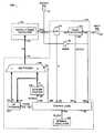
- FIG. 1a block diagram of a system (or circuit) 100 is shown in accordance with a preferred embodiment of the present invention.
- the circuit 100may be implemented as an integrated circuit (IC) on a single package (or die).
- the circuit 100may allow an operating frequency of a self-contained, on-chip oscillator to be set via a single pin.
- the present inventionmay also provide a method for tuning an oscillator.
- the circuit 100generally comprises a control block (or circuit) 102 and an output block (or circuit) 104 .
- the control circuit 102may have an input 110 that may receive a signal (e.g., IN), an input 112 that may receive a signal (e.g., OUT) and an output 114 that may present a signal (e.g., CS).
- the signal INmay be a periodic signal having a reference frequency.
- the signal OUTmay be implemented as an output signal that may oscillate at a particular frequency.
- the signal CSmay be implemented as a single-bit or a multi-bit control signal.
- the frequency of the signal OUTmay be tuned in response to the frequency of the signal IN.
- the circuit 102may be configured to generate the signal CS in response to the signals IN and OUT.
- the control circuit 102may be configured to tune the frequency of the signal OUT.
- the output circuit 104may have an input 116 that may receive the signal CS and an output 118 that may present the signal OUT.
- the signal CSmay be used to tune the circuit 104 .
- the circuit 104may be configured to generate the signal OUT in response to the signal CS.
- the signal INmay be received on a pin (or terminal) 120 .
- the signal OUTmay be presented on a pin 122 .
- the output circuit 104may be implemented as a digitally tuned oscillator. However, other types of oscillators may be implemented accordingly to meet the design criteria of a particular application.
- the control circuit 102may comprise a phase detector 121 , a control logic block (or circuit) 150 , an oscillator 152 , a counter 154 , a storage device it 156 , a divide block (or circuit) 157 and a multiplexer 158 .
- the phase detector 121may be configured to detect and compare a phase of the signal IN with a phase of the signal OUT.
- the phase detector 121may have an input 122 that may receive the signal IN, an input 124 that may receive the signal OUT through the divider 157 and an output 126 that may present a signal (e.g., DETECT).
- the phase detector 121may be configured to generate the signal DETECT in response to the signal IN and the signal OUT.
- the signal DETECTmay be implemented to indicate phase and/or frequency differences between the signal IN and the signal OUT.
- the signal DETECTmay be implemented as a single-bit or a multi-bit signal. The comparison of (difference between) the phases may be presented as the signal DETECT.
- the control logic 150may have an input 130 that may receive the signal IN and an input 132 that may receive the signal DETECT.
- the control logic 150may also have an input 160 that may receive a signal (e.g., IN_CLK), an output 162 that may present a signal (e.g., STORE), an output 164 that may present a signal (e.g., INC/DEC), an output 166 that may present a signal (e.g., SEL) and an output 167 that may present a divide signal (e.g., N).
- the signal IN_CLKmay be an internal oscillator signal.
- the signals STORE, INC/DEC, N and SELmay be control signals.
- the control logic 150may be configured to generate the signals STORE, INC/DEC and SEL in response to one or more of the signals IN, DETECT and IN_CLK.
- the oscillator 152may be implemented as an internal oscillator.
- the control logic 150may be clocked by the internal oscillator 152 via the signal IN_CLK.
- the frequency (or accuracy) of the signal IN_CLKis generally non-critical because the signal IN_CLK generally controls the timing of calibration operational steps, not the frequency of the output signal OUT.
- the counter 154may be implemented as an up/down counter.
- the counter 154may have an input 168 that may receive the signal INC/DEC.
- the counter 154may also have an output 170 that may present a signal (e.g., A).
- the counter 154may generate the signal A in response to the signal INC/DEC.
- the signal Amay be a configuration (or calibration) value for the circuit 100 .
- the storage device 156may be implemented as a non-volatile storage device (e.g., EEPROM, Flash, Single-poly EPROM, other non-volatile floating gate technologies, etc.). RAM storage where the contents of the RAM are maintained for an extended period (more than 1 year) by an external battery source would also be within the scope contemplated by the present invention as well as any method of memory that is erasable and electrically programmable.
- the storage device 156may be configured to store a configuration (or calibration) value of the circuit 100 .
- the storage device 156may have an input 172 that may receive the signal STORE and an input 174 that may receive the signal A.
- the storage device 156may also have an output 176 that may present a signal (e.g., B).
- the storage device 156may be configured to generate (modify) the signal B in response to the signal STORE and the signal A.
- the storage device 156may be configured to store the value A when prompted via the signal STORE.
- the storage device 156may also be configured to present the value B during an operational (e.g., non-calibration) mode of the circuit 100 .
- the multiplexer 158may have a first input that may receive the signal A, a second input that may receive the signal B, a select input that may receive the signal SEL and an output that may present the signal CS.
- the signals A and Bmay be implemented as multi-bit or single-bit signals.
- the multiplexer 158generally passes either the signal A or the signal B as the signal CS in response to the signal SEL.
- the signal CSmay be implemented as a multi-bit or single-bit signal.
- the device 100may be configured to enter a calibration mode. While in the calibration mode, the control logic 150 may assert the signal SEL having a first state that may cause the multiplexer 158 to route (or pass) the first input (e.g., the signal A) to the output (e.g., the signal CS). The multiplexer 158 may pass a digital value of the signal A from the up/down counter 154 to the digitally tuned oscillator 104 . The control logic 150 may increment or decrement the counter 154 via the signal INC/DEC.
- the counter 154may be incremented/decremented until the phase detector 121 indicates that the frequency IN and the frequency OUT (from the digitally tuned oscillator 104 ) are similar in response to a predetermined criteria.
- the accuracy of the frequency matchmay be determined, in one example, by the resolution of counter 154 .
- the counter 154may also set the step size for frequency adjustments applied to the oscillator 104 .
- the circuit 100may be implemented as a phase-lock loop (PLL).
- PLL 100may be “locked” when the output DETECT (of the phase detector 121 ) is within a predetermined criteria.
- the control logic 150may implement the signal INC/DEC to stop the counter 154 .
- the control logic 150may then activate the signal STORE.
- the signal STOREmay cause the digital value A from the up/down counter 154 to be stored in the non-volatile storage device 156 .
- the control logic 150may control the device 100 to exit the calibration mode and enter a normal operation mode.
- the control logic 150may assert the signal SEL having a second state that may cause the multiplexer 158 to route the second input (e.g., the signal B) to the output (e.g., the signal CS).
- the multiplexer 158may then pass the value B as the signal CS to the oscillator 104 .
- the circuit 100may use the value B stored in the non-volatile storage device 156 for tuning the oscillator 104 , via the signal CS.
- the device 100may continue to generate the signal OUT having the frequency similar to the signal IN even when the signal IN is no longer applied to the input pin 120 .
- the control logic 150may be implemented as a state machine, a microcontroller, dedicated logic, or other appropriate type of device to meet the design criteria of a particular implementation.
- the control logic 150may implement various search methods for controlling the counter 154 to achieve loop lock.
- the control logic 150may implement a simple up/down ramp, binary search, or other appropriate method.
- the control logic 150may be configured to wait a predetermined amount of time (e.g., employ a time constant) after every frequency step (e.g., a modification of the output A) of the counter 154 to allow the phase detector 121 to settle.
- the input pin 120e.g., the signal IN
- output pin 122e.g., the signal OUT
- a tri-state buffermay be connected between the signal OUT and the common pin. The tri-state buffer may be in a high-impedance state (disabled) for the calibration mode and enabled for the operational mode.
- the device 100may also be configured to notify a user when calibration is finished. For example, the device 100 may gate the signal OUT off during calibration, and on when calibration is complete, where the onset of the oscillator signal OUT on the pin 122 may indicate the operational mode.
- the control logic 150may be configured to generate a signal (e.g., DONE) that may be presented to an additional output pin (not shown) indicating a current mode of the circuit 100 (e.g., calibrate or operational mode).
- the device 100may also be configured to present the signal OUT at terminal 122 having a frequency that is a multiple of the calibration frequency applied as the signal IN.
- the divide circuit 157may be implemented as a “divide by N” counter interposed between the input 112 of the circuit 102 and the input 124 of the circuit 121 .
- the divider 157may be controlled by the signal N received from the control logic 150 .
- the frequency of the signal OUTis generally twice the frequency of the applied calibration signal IN.
- the multiplicative valuesmay be controlled using additional input pins to the control logic 150 (not shown).
- Frequency multiplicationmay make the circuit 100 more useful since a common lab function generator may not generate a high enough frequency for calibration. For example, if an output frequency of 48 MHz is needed, but a particular lab generator can only generate 20 MHz, the circuit 100 may be configured to multiply by 4 while receiving a 12 MHz calibration signal.
- a circuit 200is shown illustrating an implementation of the circuit 100 .
- the circuit 200may provide a stand-alone implementation of the circuit 100 .
- the circuit 200may be implemented as a single package that may be easily tuned.
- the reference frequency INmay be applied to the pin 120 .
- the reference frequency signal INmay be removed from the pin 120 .
- the output pin 122may then present a signal with substantially the same frequency as applied via the signal IN (e.g., within a predetermined oscillator tolerance). Alternately, the absence or presence of an oscillator signal OUT at the terminal 122 may be used as a calibrate/operate indication.
- the package 200may also have a pin 204 that may be coupled to a supply voltage VCC and a pin 206 that may be coupled to the ground GND.
- the flow chart 300may illustrate a tuning procedure of the circuit 100 and/or 200 .
- the method 300generally comprises a decision state 302 , a state 304 , a state 306 , a state 308 , a decision state 310 , a state 312 , a decision state 314 , a state 316 , a decision state 318 , a state 320 , a state 322 and a state 324 .
- the state 304may represent the normal operation mode.
- the states 306 - 324may represent steps of the calibration operation mode.
- the method 300may determine whether the signal IN is present. When the signal IN is not detected the method 300 may continue to the state 304 . While in the state 304 , the method 300 may allow the circuit 100 to operate in a normal operation mode. While in the normal operation mode (e.g., the state 304 ) the circuit 100 may allow the multiplexer 154 to select the stored value B and the oscillator 104 may be tuned using the stored value from the non-volatile storage 156 to generate the output frequency OUT. The state 304 may return to the decision state 302 periodically.
- the normal operation modee.g., the state 304
- the circuit 100may allow the multiplexer 154 to select the stored value B and the oscillator 104 may be tuned using the stored value from the non-volatile storage 156 to generate the output frequency OUT.
- the state 304may return to the decision state 302 periodically.
- the method 300may proceed to the state 306 . While in the state 306 , the method 300 may set the counter 154 to an initial value. The method 300 may then proceed to the state 308 . While in the state 308 , the method 300 may set the multiplexer 158 to pass the counter value A. The method 300 may then proceed to the decision state 310 after a predetermined settling interval.
- the method 300may determine whether the input frequency IN is greater than the output frequency OUT. When the input frequency IN is greater than the output frequency OUT, the method 300 may increase the count of the counter 154 while at the state 312 . The method 300 may then return to the decision state 310 . When the input frequency IN is not greater than the output frequency OUT, the method 300 may proceed to the decision state 314 .
- the method 300may determine whether the input frequency IN is less than the output frequency OUT. When the input frequency IN is less than the output frequency OUT, the method 300 may decrease the count of the counter 154 while at the state 316 . The method 300 may then return to the decision state 310 . When the input frequency IN is not greater than and not less than the output frequency OUT, the method 300 ,may proceed to the decision state 318 .
- the method 300may determine whether the input frequency IN is equal to the output frequency OUT. When the output frequency OUT is not equal to the input frequency IN, the method 300 may then return to the decision state 310 . When the input frequency IN is equal to the output frequency OUT, the method 300 may proceed to the state 320 .
- the state 318may respond to a predetermined criteria (e.g., a predetermined tolerance).
- the method 300may freeze the counter 154 . The method 300 may then proceed to the state 322 . While in the state 322 , the method 300 may write the current value (e.g., the value A) from the counter 154 into the non-volatile storage 156 . The method 300 may then proceed to the state 324 . While in the state 324 , the method 300 may switch the multiplexer. 158 to the second input to route the value B from the storage 156 to the oscillator 104 . The method 300 may then return to the state 304 .
- the current valuee.g., the value A
- the method 300may switch the multiplexer. 158 to the second input to route the value B from the storage 156 to the oscillator 104 .
- the method 300may then return to the state 304 .
- the circuit 100may tune (set) the operating frequency of an on-chip oscillator using a single pin.
- the circuit 100may provide in-system tuning.
- the circuit 100may have a simple implementation.
- the circuit 100may allow an external reference frequency to set the operating frequency of the on-chip oscillator.
- the circuit 100may allow the input and output frequencies to be shared on a single pin, further reducing pin count.
- the circuit 100may provide an accuracy of the output frequency OUT determined by a frequency accuracy of an input signal plus the internal resolution of the counter 154 . Additionally, the circuit 100 may eliminate special modes for tuning.
- the various signals of the present inventionare generally “on” (e.g., a digital HIGH, or 1) or “off” (e.g., a digital LOW, or 0).
- the particular polarities of the on (e.g., asserted) and off (e.g., de-asserted) states of the signalsmay be adjusted (e.g., reversed) accordingly to meet the design criteria of a particular implementation.
- invertersmay be added to change a particular polarity of the signals.
Landscapes
- Stabilization Of Oscillater, Synchronisation, Frequency Synthesizers (AREA)
Abstract
Description
Claims (23)
Priority Applications (1)
| Application Number | Priority Date | Filing Date | Title |
|---|---|---|---|
| US09/981,448US6670852B1 (en) | 2001-10-17 | 2001-10-17 | Oscillator tuning method |
Applications Claiming Priority (1)
| Application Number | Priority Date | Filing Date | Title |
|---|---|---|---|
| US09/981,448US6670852B1 (en) | 2001-10-17 | 2001-10-17 | Oscillator tuning method |
Publications (1)
| Publication Number | Publication Date |
|---|---|
| US6670852B1true US6670852B1 (en) | 2003-12-30 |
Family
ID=29737346
Family Applications (1)
| Application Number | Title | Priority Date | Filing Date |
|---|---|---|---|
| US09/981,448Expired - LifetimeUS6670852B1 (en) | 2001-10-17 | 2001-10-17 | Oscillator tuning method |
Country Status (1)
| Country | Link |
|---|---|
| US (1) | US6670852B1 (en) |
Cited By (56)
| Publication number | Priority date | Publication date | Assignee | Title |
|---|---|---|---|---|
| US20040232995A1 (en)* | 2003-05-02 | 2004-11-25 | Silicon Laboratories Inc. | Dual loop architecture useful for a programmable clock source and clock multiplier applications |
| US20050068118A1 (en)* | 2003-09-30 | 2005-03-31 | Silicon Laboratories, Inc. | Reconfigurable terminal |
| US20050151592A1 (en)* | 2004-01-09 | 2005-07-14 | Aaron Partridge | Frequency and/or phase compensated microelectromechanical oscillator |
| US20060056561A1 (en)* | 2004-09-15 | 2006-03-16 | Silicon Laboratories Inc. | Jitter self test |
| US20060119437A1 (en)* | 2003-05-02 | 2006-06-08 | Axel Thomsen | Voltage controlled clock synthesizer |
| US20060119402A1 (en)* | 2003-05-02 | 2006-06-08 | Axel Thomsen | Multi-frequency clock synthesizer |
| US20060267701A1 (en)* | 2005-05-27 | 2006-11-30 | Robert Eilers | Method and system for dynamically calculating values for tuning of voltage-controlled crystal oscillators |
| US7187245B1 (en) | 2003-09-25 | 2007-03-06 | Cypress Semiconductor Corporation | Amplitude control for crystal oscillator |
| US20070146083A1 (en)* | 2003-05-02 | 2007-06-28 | Jerrell Hein | Calibration of oscillator devices |
| US20070188245A1 (en)* | 2006-01-24 | 2007-08-16 | Stmicroelectronics Sa | Calibrating an oscillator and corresponding calibration device |
| US7265633B1 (en) | 2004-06-14 | 2007-09-04 | Cypress Semiconductor Corporation | Open loop bandwidth test architecture and method for phase locked loop (PLL) |
| US7332976B1 (en) | 2005-02-04 | 2008-02-19 | Cypress Semiconductor Corporation | Poly-phase frequency synthesis oscillator |
| US7737724B2 (en) | 2007-04-17 | 2010-06-15 | Cypress Semiconductor Corporation | Universal digital block interconnection and channel routing |
| US7761845B1 (en) | 2002-09-09 | 2010-07-20 | Cypress Semiconductor Corporation | Method for parameterizing a user module |
| US20100182062A1 (en)* | 2009-01-21 | 2010-07-22 | Gautham Devendra Kamath | Audio processor with internal oscillator-generated audio intermediate frequency reference |
| US7765095B1 (en) | 2000-10-26 | 2010-07-27 | Cypress Semiconductor Corporation | Conditional branching in an in-circuit emulation system |
| US7770113B1 (en) | 2001-11-19 | 2010-08-03 | Cypress Semiconductor Corporation | System and method for dynamically generating a configuration datasheet |
| US7774190B1 (en) | 2001-11-19 | 2010-08-10 | Cypress Semiconductor Corporation | Sleep and stall in an in-circuit emulation system |
| US7825688B1 (en) | 2000-10-26 | 2010-11-02 | Cypress Semiconductor Corporation | Programmable microcontroller architecture(mixed analog/digital) |
| US7844437B1 (en) | 2001-11-19 | 2010-11-30 | Cypress Semiconductor Corporation | System and method for performing next placements and pruning of disallowed placements for programming an integrated circuit |
| US7893724B2 (en) | 2004-03-25 | 2011-02-22 | Cypress Semiconductor Corporation | Method and circuit for rapid alignment of signals |
| US8026739B2 (en) | 2007-04-17 | 2011-09-27 | Cypress Semiconductor Corporation | System level interconnect with programmable switching |
| US8035455B1 (en) | 2005-12-21 | 2011-10-11 | Cypress Semiconductor Corporation | Oscillator amplitude control network |
| US8040266B2 (en) | 2007-04-17 | 2011-10-18 | Cypress Semiconductor Corporation | Programmable sigma-delta analog-to-digital converter |
| US8040193B2 (en) | 2008-03-06 | 2011-10-18 | Holtek Semiconductor Inc. | Oscillation adjusting circuit and method |
| US8049569B1 (en) | 2007-09-05 | 2011-11-01 | Cypress Semiconductor Corporation | Circuit and method for improving the accuracy of a crystal-less oscillator having dual-frequency modes |
| US8067948B2 (en) | 2006-03-27 | 2011-11-29 | Cypress Semiconductor Corporation | Input/output multiplexer bus |
| US8069428B1 (en) | 2001-10-24 | 2011-11-29 | Cypress Semiconductor Corporation | Techniques for generating microcontroller configuration information |
| US8069405B1 (en) | 2001-11-19 | 2011-11-29 | Cypress Semiconductor Corporation | User interface for efficiently browsing an electronic document using data-driven tabs |
| US8069436B2 (en) | 2004-08-13 | 2011-11-29 | Cypress Semiconductor Corporation | Providing hardware independence to automate code generation of processing device firmware |
| US8078894B1 (en) | 2007-04-25 | 2011-12-13 | Cypress Semiconductor Corporation | Power management architecture, method and configuration system |
| US8078970B1 (en) | 2001-11-09 | 2011-12-13 | Cypress Semiconductor Corporation | Graphical user interface with user-selectable list-box |
| US8085067B1 (en) | 2005-12-21 | 2011-12-27 | Cypress Semiconductor Corporation | Differential-to-single ended signal converter circuit and method |
| US8089461B2 (en) | 2005-06-23 | 2012-01-03 | Cypress Semiconductor Corporation | Touch wake for electronic devices |
| US8092083B2 (en) | 2007-04-17 | 2012-01-10 | Cypress Semiconductor Corporation | Temperature sensor with digital bandgap |
| US8103497B1 (en) | 2002-03-28 | 2012-01-24 | Cypress Semiconductor Corporation | External interface for event architecture |
| US8103496B1 (en) | 2000-10-26 | 2012-01-24 | Cypress Semicondutor Corporation | Breakpoint control in an in-circuit emulation system |
| US8120408B1 (en) | 2005-05-05 | 2012-02-21 | Cypress Semiconductor Corporation | Voltage controlled oscillator delay cell and method |
| US8130025B2 (en) | 2007-04-17 | 2012-03-06 | Cypress Semiconductor Corporation | Numerical band gap |
| US8149048B1 (en) | 2000-10-26 | 2012-04-03 | Cypress Semiconductor Corporation | Apparatus and method for programmable power management in a programmable analog circuit block |
| US8160864B1 (en) | 2000-10-26 | 2012-04-17 | Cypress Semiconductor Corporation | In-circuit emulator and pod synchronized boot |
| US8176296B2 (en) | 2000-10-26 | 2012-05-08 | Cypress Semiconductor Corporation | Programmable microcontroller architecture |
| US8242849B1 (en)* | 2011-03-30 | 2012-08-14 | Silicon Laboratories Inc. | Compensation for crystal offset in PLL-based crystal oscillators |
| US8286125B2 (en) | 2004-08-13 | 2012-10-09 | Cypress Semiconductor Corporation | Model for a hardware device-independent method of defining embedded firmware for programmable systems |
| WO2012151313A3 (en)* | 2011-05-02 | 2013-01-24 | Texas Instruments Incorporated | Apparatus and method to hold pll output frequency when input clock is lost |
| US8402313B1 (en) | 2002-05-01 | 2013-03-19 | Cypress Semiconductor Corporation | Reconfigurable testing system and method |
| US8499270B1 (en) | 2007-04-25 | 2013-07-30 | Cypress Semiconductor Corporation | Configuration of programmable IC design elements |
| US8516025B2 (en) | 2007-04-17 | 2013-08-20 | Cypress Semiconductor Corporation | Clock driven dynamic datapath chaining |
| US8533677B1 (en) | 2001-11-19 | 2013-09-10 | Cypress Semiconductor Corporation | Graphical user interface for dynamically reconfiguring a programmable device |
| US8884673B1 (en)* | 2013-10-04 | 2014-11-11 | Ememory Technology Inc. | Clock trimming apparatus and associated clock trimming method |
| US9448964B2 (en) | 2009-05-04 | 2016-09-20 | Cypress Semiconductor Corporation | Autonomous control in a programmable system |
| US9564902B2 (en) | 2007-04-17 | 2017-02-07 | Cypress Semiconductor Corporation | Dynamically configurable and re-configurable data path |
| US9720805B1 (en) | 2007-04-25 | 2017-08-01 | Cypress Semiconductor Corporation | System and method for controlling a target device |
| WO2019231523A1 (en)* | 2018-05-31 | 2019-12-05 | Wiliot, LTD. | Oscillator calibration from over-the air signals |
| US10700718B2 (en) | 2018-07-19 | 2020-06-30 | Wiliot, LTD. | Frequency detection for over-the-air calibration of oscillators |
| US10698662B2 (en) | 2001-11-15 | 2020-06-30 | Cypress Semiconductor Corporation | System providing automatic source code generation for personalization and parameterization of user modules |
Citations (2)
| Publication number | Priority date | Publication date | Assignee | Title |
|---|---|---|---|---|
| US5892408A (en)* | 1997-01-31 | 1999-04-06 | Binder; Yehuda | Method and system for calibrating a crystal oscillator |
| US6345079B1 (en)* | 1997-10-29 | 2002-02-05 | Victor Company Of Japan, Ltd. | Clock signal generation apparatus |
- 2001
- 2001-10-17USUS09/981,448patent/US6670852B1/ennot_activeExpired - Lifetime
Patent Citations (2)
| Publication number | Priority date | Publication date | Assignee | Title |
|---|---|---|---|---|
| US5892408A (en)* | 1997-01-31 | 1999-04-06 | Binder; Yehuda | Method and system for calibrating a crystal oscillator |
| US6345079B1 (en)* | 1997-10-29 | 2002-02-05 | Victor Company Of Japan, Ltd. | Clock signal generation apparatus |
Non-Patent Citations (5)
| Title |
|---|
| "1kHz to 30MHz Resistor Set SOT-23 Oscillator", Initial Release Final Electrical Specifications LTC1799, Linear Technology Corporation, Jan. 2001, pp. 1-4. |
| "CY7C63221/31A enCoRe(TM) USB Low-Speed USB Peripheral Controller", Cypress Semiconductor Corporation, Jan. 16, 2001, pp. 1-42. |
| "CY7C63221/31A enCoRe™ USB Low-Speed USB Peripheral Controller", Cypress Semiconductor Corporation, Jan. 16, 2001, pp. 1-42. |
| CY7C63722/23-CY7C63742/43 enCoRe(TM) USB Combination Low-Speed USB & PS/2 Peripheral Controller, Cypress Semiconductor Corporation, May 25, 2000, pp. 1-48. |
| CY7C63722/23—CY7C63742/43 enCoRe™ USB Combination Low-Speed USB & PS/2 Peripheral Controller, Cypress Semiconductor Corporation, May 25, 2000, pp. 1-48. |
Cited By (90)
| Publication number | Priority date | Publication date | Assignee | Title |
|---|---|---|---|---|
| US8736303B2 (en) | 2000-10-26 | 2014-05-27 | Cypress Semiconductor Corporation | PSOC architecture |
| US9766650B2 (en) | 2000-10-26 | 2017-09-19 | Cypress Semiconductor Corporation | Microcontroller programmable system on a chip with programmable interconnect |
| US8176296B2 (en) | 2000-10-26 | 2012-05-08 | Cypress Semiconductor Corporation | Programmable microcontroller architecture |
| US8160864B1 (en) | 2000-10-26 | 2012-04-17 | Cypress Semiconductor Corporation | In-circuit emulator and pod synchronized boot |
| US8149048B1 (en) | 2000-10-26 | 2012-04-03 | Cypress Semiconductor Corporation | Apparatus and method for programmable power management in a programmable analog circuit block |
| US8103496B1 (en) | 2000-10-26 | 2012-01-24 | Cypress Semicondutor Corporation | Breakpoint control in an in-circuit emulation system |
| US8555032B2 (en) | 2000-10-26 | 2013-10-08 | Cypress Semiconductor Corporation | Microcontroller programmable system on a chip with programmable interconnect |
| US7765095B1 (en) | 2000-10-26 | 2010-07-27 | Cypress Semiconductor Corporation | Conditional branching in an in-circuit emulation system |
| US8358150B1 (en) | 2000-10-26 | 2013-01-22 | Cypress Semiconductor Corporation | Programmable microcontroller architecture(mixed analog/digital) |
| US10261932B2 (en) | 2000-10-26 | 2019-04-16 | Cypress Semiconductor Corporation | Microcontroller programmable system on a chip |
| US7825688B1 (en) | 2000-10-26 | 2010-11-02 | Cypress Semiconductor Corporation | Programmable microcontroller architecture(mixed analog/digital) |
| US9843327B1 (en) | 2000-10-26 | 2017-12-12 | Cypress Semiconductor Corporation | PSOC architecture |
| US10725954B2 (en) | 2000-10-26 | 2020-07-28 | Monterey Research, Llc | Microcontroller programmable system on a chip |
| US10020810B2 (en) | 2000-10-26 | 2018-07-10 | Cypress Semiconductor Corporation | PSoC architecture |
| US10248604B2 (en) | 2000-10-26 | 2019-04-02 | Cypress Semiconductor Corporation | Microcontroller programmable system on a chip |
| US8793635B1 (en) | 2001-10-24 | 2014-07-29 | Cypress Semiconductor Corporation | Techniques for generating microcontroller configuration information |
| US10466980B2 (en) | 2001-10-24 | 2019-11-05 | Cypress Semiconductor Corporation | Techniques for generating microcontroller configuration information |
| US8069428B1 (en) | 2001-10-24 | 2011-11-29 | Cypress Semiconductor Corporation | Techniques for generating microcontroller configuration information |
| US8078970B1 (en) | 2001-11-09 | 2011-12-13 | Cypress Semiconductor Corporation | Graphical user interface with user-selectable list-box |
| US10698662B2 (en) | 2001-11-15 | 2020-06-30 | Cypress Semiconductor Corporation | System providing automatic source code generation for personalization and parameterization of user modules |
| US8069405B1 (en) | 2001-11-19 | 2011-11-29 | Cypress Semiconductor Corporation | User interface for efficiently browsing an electronic document using data-driven tabs |
| US8370791B2 (en) | 2001-11-19 | 2013-02-05 | Cypress Semiconductor Corporation | System and method for performing next placements and pruning of disallowed placements for programming an integrated circuit |
| US7770113B1 (en) | 2001-11-19 | 2010-08-03 | Cypress Semiconductor Corporation | System and method for dynamically generating a configuration datasheet |
| US7774190B1 (en) | 2001-11-19 | 2010-08-10 | Cypress Semiconductor Corporation | Sleep and stall in an in-circuit emulation system |
| US8533677B1 (en) | 2001-11-19 | 2013-09-10 | Cypress Semiconductor Corporation | Graphical user interface for dynamically reconfiguring a programmable device |
| US7844437B1 (en) | 2001-11-19 | 2010-11-30 | Cypress Semiconductor Corporation | System and method for performing next placements and pruning of disallowed placements for programming an integrated circuit |
| US8103497B1 (en) | 2002-03-28 | 2012-01-24 | Cypress Semiconductor Corporation | External interface for event architecture |
| US8402313B1 (en) | 2002-05-01 | 2013-03-19 | Cypress Semiconductor Corporation | Reconfigurable testing system and method |
| US7761845B1 (en) | 2002-09-09 | 2010-07-20 | Cypress Semiconductor Corporation | Method for parameterizing a user module |
| US20040232995A1 (en)* | 2003-05-02 | 2004-11-25 | Silicon Laboratories Inc. | Dual loop architecture useful for a programmable clock source and clock multiplier applications |
| US20060119402A1 (en)* | 2003-05-02 | 2006-06-08 | Axel Thomsen | Multi-frequency clock synthesizer |
| US20060119437A1 (en)* | 2003-05-02 | 2006-06-08 | Axel Thomsen | Voltage controlled clock synthesizer |
| US20070146083A1 (en)* | 2003-05-02 | 2007-06-28 | Jerrell Hein | Calibration of oscillator devices |
| US7436227B2 (en) | 2003-05-02 | 2008-10-14 | Silicon Laboratories Inc. | Dual loop architecture useful for a programmable clock source and clock multiplier applications |
| US7295077B2 (en) | 2003-05-02 | 2007-11-13 | Silicon Laboratories Inc. | Multi-frequency clock synthesizer |
| US7288998B2 (en) | 2003-05-02 | 2007-10-30 | Silicon Laboratories Inc. | Voltage controlled clock synthesizer |
| US7825708B2 (en) | 2003-05-02 | 2010-11-02 | Silicon Laboratories Inc. | Dual loop architecture useful for a programmable clock source and clock multiplier applications |
| US7187245B1 (en) | 2003-09-25 | 2007-03-06 | Cypress Semiconductor Corporation | Amplitude control for crystal oscillator |
| US20050068118A1 (en)* | 2003-09-30 | 2005-03-31 | Silicon Laboratories, Inc. | Reconfigurable terminal |
| US7224236B2 (en) | 2004-01-09 | 2007-05-29 | Robert Bosch Gmbh | Frequency and/or phase compensated microelectromechanical oscillator |
| US6995622B2 (en) | 2004-01-09 | 2006-02-07 | Robert Bosh Gmbh | Frequency and/or phase compensated microelectromechanical oscillator |
| US20050151592A1 (en)* | 2004-01-09 | 2005-07-14 | Aaron Partridge | Frequency and/or phase compensated microelectromechanical oscillator |
| US7221230B2 (en) | 2004-01-09 | 2007-05-22 | Robert Bosch Gmbh | Frequency and/or phase compensated microelectromechanical oscillator |
| US7893724B2 (en) | 2004-03-25 | 2011-02-22 | Cypress Semiconductor Corporation | Method and circuit for rapid alignment of signals |
| US7265633B1 (en) | 2004-06-14 | 2007-09-04 | Cypress Semiconductor Corporation | Open loop bandwidth test architecture and method for phase locked loop (PLL) |
| US8069436B2 (en) | 2004-08-13 | 2011-11-29 | Cypress Semiconductor Corporation | Providing hardware independence to automate code generation of processing device firmware |
| US8286125B2 (en) | 2004-08-13 | 2012-10-09 | Cypress Semiconductor Corporation | Model for a hardware device-independent method of defining embedded firmware for programmable systems |
| US7522690B2 (en) | 2004-09-15 | 2009-04-21 | Silicon Laboratories Inc. | Jitter self test |
| US20060056561A1 (en)* | 2004-09-15 | 2006-03-16 | Silicon Laboratories Inc. | Jitter self test |
| US7332976B1 (en) | 2005-02-04 | 2008-02-19 | Cypress Semiconductor Corporation | Poly-phase frequency synthesis oscillator |
| US8085100B2 (en) | 2005-02-04 | 2011-12-27 | Cypress Semiconductor Corporation | Poly-phase frequency synthesis oscillator |
| US8120408B1 (en) | 2005-05-05 | 2012-02-21 | Cypress Semiconductor Corporation | Voltage controlled oscillator delay cell and method |
| US20060267701A1 (en)* | 2005-05-27 | 2006-11-30 | Robert Eilers | Method and system for dynamically calculating values for tuning of voltage-controlled crystal oscillators |
| US8089461B2 (en) | 2005-06-23 | 2012-01-03 | Cypress Semiconductor Corporation | Touch wake for electronic devices |
| US8085067B1 (en) | 2005-12-21 | 2011-12-27 | Cypress Semiconductor Corporation | Differential-to-single ended signal converter circuit and method |
| US8035455B1 (en) | 2005-12-21 | 2011-10-11 | Cypress Semiconductor Corporation | Oscillator amplitude control network |
| US7821345B2 (en)* | 2006-01-24 | 2010-10-26 | Stmicroelectronics Sa | Calibrating an oscillator and corresponding calibration device |
| US20070188245A1 (en)* | 2006-01-24 | 2007-08-16 | Stmicroelectronics Sa | Calibrating an oscillator and corresponding calibration device |
| US8067948B2 (en) | 2006-03-27 | 2011-11-29 | Cypress Semiconductor Corporation | Input/output multiplexer bus |
| US8717042B1 (en) | 2006-03-27 | 2014-05-06 | Cypress Semiconductor Corporation | Input/output multiplexer bus |
| US8516025B2 (en) | 2007-04-17 | 2013-08-20 | Cypress Semiconductor Corporation | Clock driven dynamic datapath chaining |
| US8026739B2 (en) | 2007-04-17 | 2011-09-27 | Cypress Semiconductor Corporation | System level interconnect with programmable switching |
| US8040266B2 (en) | 2007-04-17 | 2011-10-18 | Cypress Semiconductor Corporation | Programmable sigma-delta analog-to-digital converter |
| US8130025B2 (en) | 2007-04-17 | 2012-03-06 | Cypress Semiconductor Corporation | Numerical band gap |
| US8092083B2 (en) | 2007-04-17 | 2012-01-10 | Cypress Semiconductor Corporation | Temperature sensor with digital bandgap |
| US7737724B2 (en) | 2007-04-17 | 2010-06-15 | Cypress Semiconductor Corporation | Universal digital block interconnection and channel routing |
| US9564902B2 (en) | 2007-04-17 | 2017-02-07 | Cypress Semiconductor Corporation | Dynamically configurable and re-configurable data path |
| US8476928B1 (en) | 2007-04-17 | 2013-07-02 | Cypress Semiconductor Corporation | System level interconnect with programmable switching |
| US8078894B1 (en) | 2007-04-25 | 2011-12-13 | Cypress Semiconductor Corporation | Power management architecture, method and configuration system |
| US8499270B1 (en) | 2007-04-25 | 2013-07-30 | Cypress Semiconductor Corporation | Configuration of programmable IC design elements |
| US8909960B1 (en) | 2007-04-25 | 2014-12-09 | Cypress Semiconductor Corporation | Power management architecture, method and configuration system |
| US9720805B1 (en) | 2007-04-25 | 2017-08-01 | Cypress Semiconductor Corporation | System and method for controlling a target device |
| US8049569B1 (en) | 2007-09-05 | 2011-11-01 | Cypress Semiconductor Corporation | Circuit and method for improving the accuracy of a crystal-less oscillator having dual-frequency modes |
| US8040193B2 (en) | 2008-03-06 | 2011-10-18 | Holtek Semiconductor Inc. | Oscillation adjusting circuit and method |
| US20100182062A1 (en)* | 2009-01-21 | 2010-07-22 | Gautham Devendra Kamath | Audio processor with internal oscillator-generated audio intermediate frequency reference |
| US8452429B2 (en) | 2009-01-21 | 2013-05-28 | Cirrus Logic, Inc. | Audio processor with internal oscillator-generated audio intermediate frequency reference |
| US9448964B2 (en) | 2009-05-04 | 2016-09-20 | Cypress Semiconductor Corporation | Autonomous control in a programmable system |
| US8242849B1 (en)* | 2011-03-30 | 2012-08-14 | Silicon Laboratories Inc. | Compensation for crystal offset in PLL-based crystal oscillators |
| WO2012151313A3 (en)* | 2011-05-02 | 2013-01-24 | Texas Instruments Incorporated | Apparatus and method to hold pll output frequency when input clock is lost |
| CN103650348A (en)* | 2011-05-02 | 2014-03-19 | 德克萨斯仪器股份有限公司 | Apparatus and method for maintaining PLL output frequency when input clock is lost |
| US8446193B2 (en) | 2011-05-02 | 2013-05-21 | National Semiconductor Corporation | Apparatus and method to hold PLL output frequency when input clock is lost |
| CN104518787B (en)* | 2013-10-04 | 2017-11-07 | 力旺电子股份有限公司 | Clock adjusting device and related clock adjusting method thereof |
| CN104518787A (en)* | 2013-10-04 | 2015-04-15 | 力旺电子股份有限公司 | Clock adjustment device and related clock adjustment method |
| TWI508455B (en)* | 2013-10-04 | 2015-11-11 | Ememory Technology Inc | Clock trimming apparatus and associated clock trimming method |
| US8884673B1 (en)* | 2013-10-04 | 2014-11-11 | Ememory Technology Inc. | Clock trimming apparatus and associated clock trimming method |
| WO2019231523A1 (en)* | 2018-05-31 | 2019-12-05 | Wiliot, LTD. | Oscillator calibration from over-the air signals |
| CN111971900A (en)* | 2018-05-31 | 2020-11-20 | 威利奥特有限公司 | Oscillator calibration from over-the-air signals |
| US10886929B2 (en) | 2018-05-31 | 2021-01-05 | Wiliot, LTD. | Oscillator calibration from over-the-air signals for low power frequency/time references wireless radios |
| US11329658B2 (en) | 2018-05-31 | 2022-05-10 | Wiliot, LTD. | Oscillator calibration from over-the air signals |
| US10700718B2 (en) | 2018-07-19 | 2020-06-30 | Wiliot, LTD. | Frequency detection for over-the-air calibration of oscillators |
Similar Documents
| Publication | Publication Date | Title |
|---|---|---|
| US6670852B1 (en) | Oscillator tuning method | |
| US5686864A (en) | Method and apparatus for controlling a voltage controlled oscillator tuning range in a frequency synthesizer | |
| US7209013B2 (en) | Systems and methods for self-calibration | |
| US7602223B2 (en) | Delay-locked loop circuit and method of generating multiplied clock therefrom | |
| US5577086A (en) | Clock signal generation circuit capable of operating at high speed with high frequency | |
| US7831873B1 (en) | Method and apparatus for detecting sudden temperature/voltage changes in integrated circuits | |
| US9042854B2 (en) | Apparatus and methods for tuning a voltage controlled oscillator | |
| US8497741B2 (en) | High accuracy RC oscillator | |
| KR101632467B1 (en) | Calibrated relaxation oscillator using a pll | |
| US6859028B2 (en) | Design-for-test modes for a phase locked loop | |
| US6133770A (en) | Phase locked loop circuit | |
| US20110193640A1 (en) | Semiconductor device | |
| US7804371B2 (en) | Systems, modules, chips, circuits and methods with delay trim value updates on power-up | |
| US7757110B2 (en) | Timer circuit that bypasses frequency divider in response to receiving short-time mode instruction on dual-function external terminal | |
| US10447253B2 (en) | High performance PLL based on PVT independent stable oscillator | |
| US6545545B1 (en) | Voltage-controlled oscillator frequency auto-calibrating system | |
| US6177842B1 (en) | Stabilized phase lock detection circuits and methods of operation therefor | |
| US6518848B2 (en) | Oscillation stop detection circuit | |
| US7199653B2 (en) | Semiconductor device with operation mode set by external resistor | |
| US6597162B2 (en) | PLL semiconductor device with testability, and method and apparatus for testing same | |
| CN113411084B (en) | Oscillator compensation using bias current | |
| US6900701B2 (en) | Automatic detection, selection and configuration of clock oscillator circuitry | |
| US10224941B2 (en) | Oscillation apparatus and oscillation frequency adjustment method | |
| US7091727B2 (en) | Method and IC for detecting capacitance variation | |
| US6731708B1 (en) | Clock signal control device |
Legal Events
| Date | Code | Title | Description |
|---|---|---|---|
| AS | Assignment | Owner name:CYPRESS SEMICONDUCTOR CORPORATION, CALIFORNIA Free format text:ASSIGNMENT OF ASSIGNORS INTEREST;ASSIGNOR:HAUCK, LANE T.;REEL/FRAME:012271/0324 Effective date:20011017 | |
| STCF | Information on status: patent grant | Free format text:PATENTED CASE | |
| FPAY | Fee payment | Year of fee payment:4 | |
| FPAY | Fee payment | Year of fee payment:8 | |
| AS | Assignment | Owner name:RPX CORPORATION, CALIFORNIA Free format text:ASSIGNMENT OF ASSIGNORS INTEREST;ASSIGNOR:CYPRESS SEMICONDUCTOR CORPORATION;REEL/FRAME:033119/0615 Effective date:20140604 | |
| FEPP | Fee payment procedure | Free format text:PAYOR NUMBER ASSIGNED (ORIGINAL EVENT CODE: ASPN); ENTITY STATUS OF PATENT OWNER: LARGE ENTITY | |
| FPAY | Fee payment | Year of fee payment:12 | |
| AS | Assignment | Owner name:JPMORGAN CHASE BANK, N.A., AS COLLATERAL AGENT, IL Free format text:SECURITY AGREEMENT;ASSIGNORS:RPX CORPORATION;RPX CLEARINGHOUSE LLC;REEL/FRAME:038041/0001 Effective date:20160226 | |
| AS | Assignment | Owner name:RPX CORPORATION, CALIFORNIA Free format text:RELEASE (REEL 038041 / FRAME 0001);ASSIGNOR:JPMORGAN CHASE BANK, N.A.;REEL/FRAME:044970/0030 Effective date:20171222 Owner name:RPX CLEARINGHOUSE LLC, CALIFORNIA Free format text:RELEASE (REEL 038041 / FRAME 0001);ASSIGNOR:JPMORGAN CHASE BANK, N.A.;REEL/FRAME:044970/0030 Effective date:20171222 | |
| AS | Assignment | Owner name:JEFFERIES FINANCE LLC, NEW YORK Free format text:SECURITY INTEREST;ASSIGNOR:RPX CORPORATION;REEL/FRAME:046486/0433 Effective date:20180619 | |
| AS | Assignment | Owner name:RPX CORPORATION, CALIFORNIA Free format text:RELEASE OF LIEN ON PATENTS;ASSIGNOR:JEFFERIES FINANCE LLC, AS COLLATERAL AGENT;REEL/FRAME:050777/0983 Effective date:20191021 | |
| AS | Assignment | Owner name:TAIWAN SEMICONDUCTOR MANUFACTURING CO., LTD., TAIWAN Free format text:ASSIGNMENT OF ASSIGNORS INTEREST;ASSIGNOR:RPX CORPORATION;REEL/FRAME:051842/0494 Effective date:20190919 | |
| AS | Assignment | Owner name:RPX CORPORATION, CALIFORNIA Free format text:RELEASE BY SECURED PARTY;ASSIGNOR:JEFFERIES FINANCE LLC;REEL/FRAME:054486/0422 Effective date:20201023 |