US6670258B2 - Fabrication of low leakage-current backside illuminated photodiodes - Google Patents
Fabrication of low leakage-current backside illuminated photodiodesDownload PDFInfo
- Publication number
- US6670258B2 US6670258B2US09/839,641US83964101AUS6670258B2US 6670258 B2US6670258 B2US 6670258B2US 83964101 AUS83964101 AUS 83964101AUS 6670258 B2US6670258 B2US 6670258B2
- Authority
- US
- United States
- Prior art keywords
- layer
- substrate
- gettering
- conductive
- bias electrode
- Prior art date
- Legal status (The legal status is an assumption and is not a legal conclusion. Google has not performed a legal analysis and makes no representation as to the accuracy of the status listed.)
- Expired - Lifetime, expires
Links
- 238000004519manufacturing processMethods0.000titleclaimsdescription6
- 239000000758substrateSubstances0.000claimsabstractdescription62
- 238000000034methodMethods0.000claimsabstractdescription33
- 238000005247getteringMethods0.000claimsabstractdescription25
- 230000008569processEffects0.000claimsabstractdescription17
- 229910021420polycrystalline siliconInorganic materials0.000claimsabstractdescription14
- 229920005591polysiliconPolymers0.000claimsabstractdescription14
- 230000007547defectEffects0.000claimsabstractdescription12
- 239000012535impuritySubstances0.000claimsabstractdescription12
- 238000003491arrayMethods0.000abstractdescription16
- 239000004065semiconductorSubstances0.000abstractdescription10
- 238000012545processingMethods0.000abstractdescription9
- 230000003287optical effectEffects0.000abstractdescription7
- 229910021419crystalline siliconInorganic materials0.000abstractdescription3
- 238000005530etchingMethods0.000abstractdescription3
- 230000015572biosynthetic processEffects0.000abstract1
- 229910052710siliconInorganic materials0.000description9
- 239000010703siliconSubstances0.000description9
- VYPSYNLAJGMNEJ-UHFFFAOYSA-NSilicium dioxideChemical compoundO=[Si]=OVYPSYNLAJGMNEJ-UHFFFAOYSA-N0.000description8
- XUIMIQQOPSSXEZ-UHFFFAOYSA-NSiliconChemical compound[Si]XUIMIQQOPSSXEZ-UHFFFAOYSA-N0.000description8
- 230000005684electric fieldEffects0.000description7
- 238000001514detection methodMethods0.000description5
- 239000002019doping agentSubstances0.000description5
- 238000000151depositionMethods0.000description4
- 230000008021depositionEffects0.000description4
- 238000003384imaging methodMethods0.000description4
- 239000000463materialSubstances0.000description4
- 239000000377silicon dioxideSubstances0.000description4
- 206010034972Photosensitivity reactionDiseases0.000description3
- 238000000576coating methodMethods0.000description3
- 239000002245particleSubstances0.000description3
- 230000036211photosensitivityEffects0.000description3
- 238000001020plasma etchingMethods0.000description3
- 230000005855radiationEffects0.000description3
- 230000007704transitionEffects0.000description3
- 238000010521absorption reactionMethods0.000description2
- 239000006117anti-reflective coatingSubstances0.000description2
- 230000008901benefitEffects0.000description2
- 238000006243chemical reactionMethods0.000description2
- 239000011248coating agentSubstances0.000description2
- 238000002591computed tomographyMethods0.000description2
- 239000004020conductorSubstances0.000description2
- 238000002059diagnostic imagingMethods0.000description2
- 238000009792diffusion processMethods0.000description2
- AMGQUBHHOARCQH-UHFFFAOYSA-Nindium;oxotinChemical compound[In].[Sn]=OAMGQUBHHOARCQH-UHFFFAOYSA-N0.000description2
- 229910052751metalInorganic materials0.000description2
- 239000002184metalSubstances0.000description2
- XHXFXVLFKHQFAL-UHFFFAOYSA-Nphosphoryl trichlorideChemical compoundClP(Cl)(Cl)=OXHXFXVLFKHQFAL-UHFFFAOYSA-N0.000description2
- 230000006798recombinationEffects0.000description2
- 238000005215recombinationMethods0.000description2
- 238000002310reflectometryMethods0.000description2
- 230000004044responseEffects0.000description2
- 235000012239silicon dioxideNutrition0.000description2
- 229910019213POCl3Inorganic materials0.000description1
- 230000009286beneficial effectEffects0.000description1
- 230000015556catabolic processEffects0.000description1
- 239000002800charge carrierSubstances0.000description1
- 238000003486chemical etchingMethods0.000description1
- 238000012993chemical processingMethods0.000description1
- 238000011109contaminationMethods0.000description1
- 230000008094contradictory effectEffects0.000description1
- 239000013078crystalSubstances0.000description1
- 238000006731degradation reactionMethods0.000description1
- 230000005670electromagnetic radiationEffects0.000description1
- 238000000407epitaxyMethods0.000description1
- 230000004907fluxEffects0.000description1
- 230000005251gamma rayEffects0.000description1
- 238000011065in-situ storageMethods0.000description1
- 238000010348incorporationMethods0.000description1
- 229910003437indium oxideInorganic materials0.000description1
- PJXISJQVUVHSOJ-UHFFFAOYSA-Nindium(iii) oxideChemical compound[O-2].[O-2].[O-2].[In+3].[In+3]PJXISJQVUVHSOJ-UHFFFAOYSA-N0.000description1
- 229910000765intermetallicInorganic materials0.000description1
- 238000005468ion implantationMethods0.000description1
- 150000002500ionsChemical class0.000description1
- 238000007620mathematical functionMethods0.000description1
- 150000002739metalsChemical class0.000description1
- 239000000203mixtureSubstances0.000description1
- 238000012986modificationMethods0.000description1
- 230000004048modificationEffects0.000description1
- 230000007935neutral effectEffects0.000description1
- 238000005457optimizationMethods0.000description1
- 230000003647oxidationEffects0.000description1
- 238000007254oxidation reactionMethods0.000description1
- 230000009467reductionEffects0.000description1
- 239000000126substanceSubstances0.000description1
- XOLBLPGZBRYERU-UHFFFAOYSA-Ntin dioxideChemical compoundO=[Sn]=OXOLBLPGZBRYERU-UHFFFAOYSA-N0.000description1
- 229910001887tin oxideInorganic materials0.000description1
- 238000012546transferMethods0.000description1
- 238000011282treatmentMethods0.000description1
- 238000003631wet chemical etchingMethods0.000description1
Images

Classifications
- H—ELECTRICITY
- H10—SEMICONDUCTOR DEVICES; ELECTRIC SOLID-STATE DEVICES NOT OTHERWISE PROVIDED FOR
- H10F—INORGANIC SEMICONDUCTOR DEVICES SENSITIVE TO INFRARED RADIATION, LIGHT, ELECTROMAGNETIC RADIATION OF SHORTER WAVELENGTH OR CORPUSCULAR RADIATION
- H10F71/00—Manufacture or treatment of devices covered by this subclass
- H10F71/138—Manufacture of transparent electrodes, e.g. transparent conductive oxides [TCO] or indium tin oxide [ITO] electrodes
- H—ELECTRICITY
- H10—SEMICONDUCTOR DEVICES; ELECTRIC SOLID-STATE DEVICES NOT OTHERWISE PROVIDED FOR
- H10F—INORGANIC SEMICONDUCTOR DEVICES SENSITIVE TO INFRARED RADIATION, LIGHT, ELECTROMAGNETIC RADIATION OF SHORTER WAVELENGTH OR CORPUSCULAR RADIATION
- H10F30/00—Individual radiation-sensitive semiconductor devices in which radiation controls the flow of current through the devices, e.g. photodetectors
- H10F30/20—Individual radiation-sensitive semiconductor devices in which radiation controls the flow of current through the devices, e.g. photodetectors the devices having potential barriers, e.g. phototransistors
- H10F30/21—Individual radiation-sensitive semiconductor devices in which radiation controls the flow of current through the devices, e.g. photodetectors the devices having potential barriers, e.g. phototransistors the devices being sensitive to infrared, visible or ultraviolet radiation
- H10F30/22—Individual radiation-sensitive semiconductor devices in which radiation controls the flow of current through the devices, e.g. photodetectors the devices having potential barriers, e.g. phototransistors the devices being sensitive to infrared, visible or ultraviolet radiation the devices having only one potential barrier, e.g. photodiodes
- H10F30/221—Individual radiation-sensitive semiconductor devices in which radiation controls the flow of current through the devices, e.g. photodetectors the devices having potential barriers, e.g. phototransistors the devices being sensitive to infrared, visible or ultraviolet radiation the devices having only one potential barrier, e.g. photodiodes the potential barrier being a PN homojunction
- H—ELECTRICITY
- H10—SEMICONDUCTOR DEVICES; ELECTRIC SOLID-STATE DEVICES NOT OTHERWISE PROVIDED FOR
- H10F—INORGANIC SEMICONDUCTOR DEVICES SENSITIVE TO INFRARED RADIATION, LIGHT, ELECTROMAGNETIC RADIATION OF SHORTER WAVELENGTH OR CORPUSCULAR RADIATION
- H10F39/00—Integrated devices, or assemblies of multiple devices, comprising at least one element covered by group H10F30/00, e.g. radiation detectors comprising photodiode arrays
- H10F39/011—Manufacture or treatment of image sensors covered by group H10F39/12
- H10F39/026—Wafer-level processing
- H—ELECTRICITY
- H10—SEMICONDUCTOR DEVICES; ELECTRIC SOLID-STATE DEVICES NOT OTHERWISE PROVIDED FOR
- H10F—INORGANIC SEMICONDUCTOR DEVICES SENSITIVE TO INFRARED RADIATION, LIGHT, ELECTROMAGNETIC RADIATION OF SHORTER WAVELENGTH OR CORPUSCULAR RADIATION
- H10F39/00—Integrated devices, or assemblies of multiple devices, comprising at least one element covered by group H10F30/00, e.g. radiation detectors comprising photodiode arrays
- H10F39/10—Integrated devices
- H10F39/107—Integrated devices having multiple elements covered by H10F30/00 in a repetitive configuration, e.g. radiation detectors comprising photodiode arrays
- H—ELECTRICITY
- H10—SEMICONDUCTOR DEVICES; ELECTRIC SOLID-STATE DEVICES NOT OTHERWISE PROVIDED FOR
- H10F—INORGANIC SEMICONDUCTOR DEVICES SENSITIVE TO INFRARED RADIATION, LIGHT, ELECTROMAGNETIC RADIATION OF SHORTER WAVELENGTH OR CORPUSCULAR RADIATION
- H10F39/00—Integrated devices, or assemblies of multiple devices, comprising at least one element covered by group H10F30/00, e.g. radiation detectors comprising photodiode arrays
- H10F39/10—Integrated devices
- H10F39/12—Image sensors
- H10F39/18—Complementary metal-oxide-semiconductor [CMOS] image sensors; Photodiode array image sensors
- H—ELECTRICITY
- H10—SEMICONDUCTOR DEVICES; ELECTRIC SOLID-STATE DEVICES NOT OTHERWISE PROVIDED FOR
- H10F—INORGANIC SEMICONDUCTOR DEVICES SENSITIVE TO INFRARED RADIATION, LIGHT, ELECTROMAGNETIC RADIATION OF SHORTER WAVELENGTH OR CORPUSCULAR RADIATION
- H10F39/00—Integrated devices, or assemblies of multiple devices, comprising at least one element covered by group H10F30/00, e.g. radiation detectors comprising photodiode arrays
- H10F39/10—Integrated devices
- H10F39/12—Image sensors
- H10F39/199—Back-illuminated image sensors
- H—ELECTRICITY
- H10—SEMICONDUCTOR DEVICES; ELECTRIC SOLID-STATE DEVICES NOT OTHERWISE PROVIDED FOR
- H10F—INORGANIC SEMICONDUCTOR DEVICES SENSITIVE TO INFRARED RADIATION, LIGHT, ELECTROMAGNETIC RADIATION OF SHORTER WAVELENGTH OR CORPUSCULAR RADIATION
- H10F39/00—Integrated devices, or assemblies of multiple devices, comprising at least one element covered by group H10F30/00, e.g. radiation detectors comprising photodiode arrays
- H10F39/80—Constructional details of image sensors
- H10F39/803—Pixels having integrated switching, control, storage or amplification elements
- H—ELECTRICITY
- H10—SEMICONDUCTOR DEVICES; ELECTRIC SOLID-STATE DEVICES NOT OTHERWISE PROVIDED FOR
- H10F—INORGANIC SEMICONDUCTOR DEVICES SENSITIVE TO INFRARED RADIATION, LIGHT, ELECTROMAGNETIC RADIATION OF SHORTER WAVELENGTH OR CORPUSCULAR RADIATION
- H10F71/00—Manufacture or treatment of devices covered by this subclass
- H—ELECTRICITY
- H10—SEMICONDUCTOR DEVICES; ELECTRIC SOLID-STATE DEVICES NOT OTHERWISE PROVIDED FOR
- H10F—INORGANIC SEMICONDUCTOR DEVICES SENSITIVE TO INFRARED RADIATION, LIGHT, ELECTROMAGNETIC RADIATION OF SHORTER WAVELENGTH OR CORPUSCULAR RADIATION
- H10F77/00—Constructional details of devices covered by this subclass
- H10F77/20—Electrodes
- H10F77/206—Electrodes for devices having potential barriers
- H—ELECTRICITY
- H10—SEMICONDUCTOR DEVICES; ELECTRIC SOLID-STATE DEVICES NOT OTHERWISE PROVIDED FOR
- H10F—INORGANIC SEMICONDUCTOR DEVICES SENSITIVE TO INFRARED RADIATION, LIGHT, ELECTROMAGNETIC RADIATION OF SHORTER WAVELENGTH OR CORPUSCULAR RADIATION
- H10F77/00—Constructional details of devices covered by this subclass
- H10F77/20—Electrodes
- H10F77/244—Electrodes made of transparent conductive layers, e.g. transparent conductive oxide [TCO] layers
- H—ELECTRICITY
- H10—SEMICONDUCTOR DEVICES; ELECTRIC SOLID-STATE DEVICES NOT OTHERWISE PROVIDED FOR
- H10F—INORGANIC SEMICONDUCTOR DEVICES SENSITIVE TO INFRARED RADIATION, LIGHT, ELECTROMAGNETIC RADIATION OF SHORTER WAVELENGTH OR CORPUSCULAR RADIATION
- H10F39/00—Integrated devices, or assemblies of multiple devices, comprising at least one element covered by group H10F30/00, e.g. radiation detectors comprising photodiode arrays
- H10F39/80—Constructional details of image sensors
- H10F39/805—Coatings
- H—ELECTRICITY
- H10—SEMICONDUCTOR DEVICES; ELECTRIC SOLID-STATE DEVICES NOT OTHERWISE PROVIDED FOR
- H10F—INORGANIC SEMICONDUCTOR DEVICES SENSITIVE TO INFRARED RADIATION, LIGHT, ELECTROMAGNETIC RADIATION OF SHORTER WAVELENGTH OR CORPUSCULAR RADIATION
- H10F77/00—Constructional details of devices covered by this subclass
- H10F77/30—Coatings
- H10F77/306—Coatings for devices having potential barriers
- Y—GENERAL TAGGING OF NEW TECHNOLOGICAL DEVELOPMENTS; GENERAL TAGGING OF CROSS-SECTIONAL TECHNOLOGIES SPANNING OVER SEVERAL SECTIONS OF THE IPC; TECHNICAL SUBJECTS COVERED BY FORMER USPC CROSS-REFERENCE ART COLLECTIONS [XRACs] AND DIGESTS
- Y02—TECHNOLOGIES OR APPLICATIONS FOR MITIGATION OR ADAPTATION AGAINST CLIMATE CHANGE
- Y02E—REDUCTION OF GREENHOUSE GAS [GHG] EMISSIONS, RELATED TO ENERGY GENERATION, TRANSMISSION OR DISTRIBUTION
- Y02E10/00—Energy generation through renewable energy sources
- Y02E10/50—Photovoltaic [PV] energy
- Y—GENERAL TAGGING OF NEW TECHNOLOGICAL DEVELOPMENTS; GENERAL TAGGING OF CROSS-SECTIONAL TECHNOLOGIES SPANNING OVER SEVERAL SECTIONS OF THE IPC; TECHNICAL SUBJECTS COVERED BY FORMER USPC CROSS-REFERENCE ART COLLECTIONS [XRACs] AND DIGESTS
- Y02—TECHNOLOGIES OR APPLICATIONS FOR MITIGATION OR ADAPTATION AGAINST CLIMATE CHANGE
- Y02P—CLIMATE CHANGE MITIGATION TECHNOLOGIES IN THE PRODUCTION OR PROCESSING OF GOODS
- Y02P70/00—Climate change mitigation technologies in the production process for final industrial or consumer products
- Y02P70/50—Manufacturing or production processes characterised by the final manufactured product
- Y—GENERAL TAGGING OF NEW TECHNOLOGICAL DEVELOPMENTS; GENERAL TAGGING OF CROSS-SECTIONAL TECHNOLOGIES SPANNING OVER SEVERAL SECTIONS OF THE IPC; TECHNICAL SUBJECTS COVERED BY FORMER USPC CROSS-REFERENCE ART COLLECTIONS [XRACs] AND DIGESTS
- Y10—TECHNICAL SUBJECTS COVERED BY FORMER USPC
- Y10T—TECHNICAL SUBJECTS COVERED BY FORMER US CLASSIFICATION
- Y10T428/00—Stock material or miscellaneous articles
- Y10T428/31504—Composite [nonstructural laminate]
- Y10T428/31652—Of asbestos
- Y10T428/31663—As siloxane, silicone or silane
Definitions
- the present inventionrelates to electromagnetic radiation detectors, and more specifically to backside-illuminated semiconductor photodiode arrays.
- a typical photodiode arrayincludes a semiconductor substrate of a first conductivity type, having a front side formed with an array of doped regions of a second, opposite conductivity type, and an opposing back side that includes a heavily-doped bias electrode layer of the first conductivity type.
- the frontside doped regionsare referred to below as gates, independent of their function as anodes or cathodes.
- the abbreviation BELis used to denote the backside bias electrode layer.
- the gate and bias electrode layersare formed internally to the crystalline semiconductor substrate. They are therefore native to and homostructural with the substrate.
- an external gate contactformed from one or more non-native, heterostructural, conducting layers external to the substrate, is formed over a portion of each of the frontside gates.
- one or more non-native, heterostructural, external back contactsmay be formed over all, or a portion of, the backside bias electrode layer.
- the gate contactsare usually formed from one or more metals, metal-silicon intermetallic compounds, or deposited, heavily-doped polysilicon, or a combination of a plurality of these materials.
- silicon photodiode arraysmay use the same materials or one or more transparent conducting materials such as indium-tin oxide, which is an amorphous typically non-stoichiometric mixture of indium oxide and tin oxide.
- an array of readout circuitsis also formed on the front surface of the substrate.
- a potential differencereferred to as a reverse bias
- a reverse biascan be applied between the gate and the bias electrode layer to produce a depletion region within the substrate extending into the substrate from the p-n junction between the gate on the front side and the substrate.
- a photodiodeis effected by the gate, the substrate and the BEL.
- External gate contacts or back contactsare ancillary elements provided to facilitate electrical connections to the photodiode array, not essential components thereof.
- Such a photodiode arraymay be configured either in a frontside-illuminated mode to receive photons from the front side or in a backside-illuminated mode to receive photons from the backside.
- the frontside-illuminated modeusually results in a lower external quantum efficiency (ratio of photocarriers collected to incident photons) than the backside-illuminated mode, because the conducting elements of the gate contacts and the readout circuits (if provided) reduce the active photosensitive area of the array on the front side.
- the entire back sidecan be used to collect incoming radiation when properly configured. All other factors being equal, enhanced photosensitivity results in increased signal-to-noise ratio.
- photocurrentis typically generated by band-to-band absorption. Photons with energy greater than the bandgap of the semiconductor substrate enter the back of the substrate and are absorbed, producing electron-hole pairs. If an electron-hole pair is generated outside the depletion region of a gate, the minority carrier (a hole in the example above) may diffuse to the edge of the depletion region beneath one of the gates. The electric field within the depletion region “collects” the hole by accelerating it towards the gate.
- the electric field“collects” the hole as above, but accelerates the electron towards the undepleted substrate, or, if the substrate is fully depleted below a gate, towards the backside bias electrode layer. In either case, the photocurrent will flow through the photodiode and the external circuitry that maintains the bias between the gate and the bias electrode layer. If readout circuitry is provided on same semiconductor substrate, the circuit elements associated with each gate will produce a signal that represents a mathematical function of the photocurrent, the quantity of charge caused by the photon absorption, or a combination of both.
- photodiode arraysIn low light-level imaging applications such as night photography, nuclear medical imaging, photon medical imaging, x-ray computed tomography and ballistic photon detection, it is critical for photodiode arrays simultaneously to exhibit high external photon conversion efficiency (defined as the ratio of photocarriers collected to photons incident on the back surface of the substrate) and extremely low reverse-bias leakage currents.
- quantum efficiencyis used below to denote external photon conversion efficiency
- leakage currentis used to denote reverse-bias leakage current.
- the input optical signaloften is in the form of short pulses, a few nanoseconds to a few microseconds in duration.
- the photodiodesit is highly beneficial for the photodiodes to have short pulse response times, often referred to collectively as transition times or, singly, as rise and fall times, in the rough order of magnitude range of 10 to 100 ns or less.
- the signal processing system associated with the photodiode arraystypically “shapes” the output pulse by integrating the photocurrent generated within a time window of fixed duration in the same order of magnitude as the length of the photopulse.
- Photodiode arrays with one or more long transition timesproduce output photocurrent pulses significantly longer than the input photopulse. These long photocurrent pulses produce smaller output pulses from the signal processing electronics than do those from faster photodiode arrays. Therefore, slow photodiode arrays may result in low output signals from the signal processing electronics and therefore degrade the signal-to-noise ratio of the image.
- the signal processing electronicsmay respond to the average photocurrent collected by a pixel over a time interval of fixed duration, longer than the duration of a single optical pulse. For these applications, longer transition times than those required for efficient single pulse detection may be acceptable.
- the bias electrode layershould be thin enough to be transparent to the incident radiation, yet sufficiently conductive to provide an equipotential surface on the back surface of the substrate adequate to maintain uniform depletion over the entire area beneath each gate.
- the bias electrode layershould also have a low density of crystallographic defects and be free from deep-level impurities. If these criteria are met, the BEL will exhibit long enough minority-carrier lifetimes to minimize recombination of photocarriers generated within the BEL, thereby maximizing the efficiency of collection of photocarriers generated therein. The BEL will therefore not be an optical “dead layer.”
- the pulse response times of the photodiodescan be minimized by using semiconductor substrates of high resistivity in the approximate range of 5 to 25 k ⁇ -cm, operated under reverse bias conditions sufficient to fully deplete the substrate under the gates. Under such full-depletion conditions, the electric field of the depletion region extends to the bias electrode layer on the back side.
- Achieving ultra-low leakage current densities, e.g., below about 1 nA/cm 2 at room temperature, of the individual photodiodesrequires reduction of the contributions to the total leakage current by (1) the substrate; (2) the back contact structure (including the bias electrode layer and any additional layers formed thereon); (3) the front surface regions between the gate regions and between the outer gates and the surrounding regions; and (4) the edges of the substrate, formed when the substrate is “diced” to form individual photodiode array chips.
- the bulk generation current of the substratemay be reduced by “gettering,” an elevated-temperature process, typically performed at 1000° C. or higher for silicon substrates, in which strained, damaged or heavily-doped layers, singly or in combination, on the back surface of the substrate attract and capture impurities or crystallographic defects. Crystallographic defects may also be annihilated by recombination during the gettering process.
- the strained, damaged or heavily-doped “gettering layer” or layersis subsequently removed, thereby removing the absorbed impurities and defects.
- Front surface generation currents in silicon photodiode arraysare usually minimized by using silicon dioxide (SiO 2 ) layers thermally grown under conditions known to produce low-leakage surfaces. These oxides are typically grown prior to, or concurrently with, the gettering process. Low-temperature (below 400° C.) treatments may be performed after gettering to optimize surface leakage.
- the bias electrode layermust be thin enough to be transparent. Such thin layers, however, are easily damaged, and damaged regions may generate leakage current very efficiently. Under fully depleted conditions, the bias electrode layer must be contain enough electrically active (i.e., charged as opposed to neutral) dopant atoms to allow it to terminate the electric field of the depletion region.
- the back surface of the crystalline semiconductor substrate, or the interface between the substrate and overlayers formed upon the back surface of the substrate to enhance the backside conductivity or to reduce reflection of incident photons,is a region where the crystal structure of the substrate is imperfectly terminated. Such regions may be capable of generating high leakage currents.
- the electric fieldpenetrates the BEL and reaches such an interface, it will efficiently collect the current generated there. Similarly, the electric field will collect leakage current generated by impurities or defects within the BEL. Undepleted regions in the BEL typically are highly-doped and will not be efficient leakage generators. Deep level impurities and defects in depleted regions of the BEL, on the other hand, may generate large leakage currents. If the BEL does not exhibit long minority carrier lifetimes, the BEL may therefore degrade the leakage current of the photodiodes.
- Edge leakage currentsare usually suppressed by providing guard structures surrounding the array of pixels. These structures collect the leakage currents generated at the diced edges before it reaches the pixels themselves.
- the present inventioncomprises fabrication of ultra-low leakage current backside-illuminated photodiode arrays wherein the transparent, conducting bias electrode layer is formed so high-temperature processing of the substrate is avoided after the wafer has been gettered.
- the component of the reverse-bias leakage current associated with strain, crystallographic defects or impurities introduced during elevated temperature processing subsequent to getteringcan be kept extremely low.
- An optically transparent, conductive bias electrode layerserving as both an optical window and a backside equipotential contact surface for the photodiodes, is fabricated by etching through the polysilicon gettering layer to a thin, heavily-doped crystalline silicon layer formed within the back of the substrate during the gettering process.
- a structure that simultaneously provides a transparent window and a conductive contact over the same area of the substrateis important in the case of fully depleted photodiodes and photodiode arrays.
- An electrical contact formed only around the periphery of the pixel area(s)would not be able to conduct the reverse-bias leakage current generated in the interior of the pixel area. It would therefore be unable to maintain full depletion.
- Bias electrode layers formed in accordance with this methodare internal (native), monocrystalline, homostructural layers formed within the semiconductor substrate.
- the interface between the BEL and the adjoining high-resistivity substrate materialdoes not terminate the crystalline lattice of the substrate, as is the case when the BEL is a polycrystalline layer or a thin metal layer.
- Interfaces produced by the present methodare inherently superior to those produced when the BEL is formed by epitaxy; it is impossible to completely eliminate crystallographic defects and interfacial impurities at epitaxial interfaces.
- Bias electrode layers formed according to the present inventionhave high minority carrier lifetimes. Photocarriers generated therein may be efficiently collected by the depletion regions beneath the gates. Therefore, these BELs can be far thicker than those fabricated using prior art. BEL thicknesses of rough order of magnitude 0.25 to 1.0 micrometer formed in silicon substrates exhibit high external quantum efficiency and low leakage currents. Such BELs are far less susceptible to damage than those with thicknesses of rough order of magnitude 0.01 micrometer formed using prior techniques.
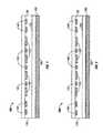
- FIG. 1illustrates a backside-illuminated photodiode structure prior to backside thinning according to one embodiment of the invention.
- FIG. 2illustrates a backside-thinned photodiode array structure according to one embodiment of the invention.
- the heavily-doped polysilicon gettering layeris etched away at approximately room temperature after wafer gettering has been accomplished.
- Thisforms an internal (native), optically transparent, conductive, homostructural bias electrode layer from the crystalline layer, doped by dopant diffusion during the gettering process, that remains within the original substrate.
- the bias electrode layerthus formed provides a transparent, conductive, internal ohmic contact to the photodiode pixels. Part of the crystalline doped layer may be removed during this process to optimize the sheet resistivity of the contact layer.
- the low-leakage current backside-illuminated photodiode array structure 100is formed within a high-resistivity silicon substrate 110 of a first conductivity type.
- the substratemay be taken to be n-type.
- an array of heavily-doped gate regions 120 of a second, opposite conductivity typeis formed near the front surface 130 of the substrate 110 .
- Additional doped regions 140each of which may have the same conductivity type as the substrate 110 or the opposite conductivity type, may be formed for purposes other than fabrication of the photodiode array itself.
- Additional low- or high-temperature processe.g., growth or deposition of oxides or other dielectric layers, chemical or plasma etching, dopant deposition, diffusion, ion implantation
- Additional low- or high-temperature processmay be performed as part of the process of defining the frontside structures of the photodiode array or ancillary devices.
- a polysilicon layer 150is deposited on the back surface 160 of the substrate 110 .
- the polysilicon layer 150may have a thicknes, in the rough order of magnitude of 0.25 to 1.5 micrometers.
- the Polysilicon layer 150is heavily doped by incorporation of impurities of the same conductivity type as the substrate 110 .
- Polysilicon dopingmay be performed in situ during deposition or subsequently by deposition of a dopant source layer (e.g., POCl 3 for n-type substrates) or other means.
- the photodiode structure 100is then subjected to a high-temperature thermal gettering cycle to transport crystallographic defects and unintentional impurities into the doped polysilicon layer 150 .
- dopant atoms f torn the polysilicon layer 150may diffuse into the back regions of the substrate 110 , forming a heavily-doped internal (native), homostructural, crystalline layer 170 within the substrate 110 which is teterred to herein as a “diffused layer”.
- the backside diffused layer 170may initially have a thickness of rough order of magnitude 0.5 to 5 micrometers, a maximum carrier concentration of rough order of magnitude 1 ⁇ 10 20 cm ⁇ 3 , and a sheet resistivity of rough order of magnitude 2 to 20 ⁇ per square.
- the doped polysilicon layer 150 and part of the backside diffused layer 170are removed. Removal of the polysilicon gettering layer 150 and the portion of the backside diffused layer 170 may be accomplished by wet-chemical etching, ion-assisted etching (plasma or reactive-ion etching) singly or in combination, or by other means.
- the backside diffused layer 170is thinned to a final thickness compatible with high external quantum efficiency, low leakage current, and conductivity adequate to facilitate uniform backside biasing.
- the backside diffused layer 170may have a final thickness of rough order of magnitude range of 0.25 to 1.0 micrometers and a sheet resistivity in the approximate range of 50 to 1000 ⁇ per square.
- the backside-thinned photodiode array structure 200includes all the frontside layers, interfaces and other features as the unfinished photodiode structure 170 of FIG. 1 . Additional layers, interfaces or features may be formed upon the front surface 130 of the substrate 110 prior to backside thinning, to provide external contacts to the gates 120 or additional doped layers 140 , to provide readout circuits, or for other purposes.
- the backside-thinned photodiode array 200includes a thinned backside diffused layer 270 that forms the bias electrode layer for the photodiode array structure. The thinning process also creates a new back surface 260 on the substrate 110 .
- one or more additional external (non-native) layers 280may be formed over the new back surface 260 to decrease the reflectivity of the structure at the optical wavelengths of interest or to enhance the backside conductivity of the structure.
- the thick, robust bias electrode layers 270 of the backside-thinned structure 200are sufficiently conductive to render such conductivity enhancement unnecessary. Therefore, a wide choice of single- or multi-layer dielectric anti-reflective coating structures may be used to optimize the external quantum efficiency of the photodiode array.
- the method described hereinhas been employed to fabricate 16-element (4 ⁇ 4 pixel square) silicon photodiode arrays with approximately 9 mm 2 (3 mm ⁇ 3 mm) pixel areas used in a commercially available gamma-ray imaging system. These devices exhibit high external quantum efficiencies—over 90% at 560 nm wavelength—when equipped with single- or multi-layer dielectric anti-reflection coatings. Production devices routinely exhibit reverse-bias leakage currents below 1 nA/cm ⁇ 2 at room temperature.
Landscapes
- Light Receiving Elements (AREA)
- Solid State Image Pick-Up Elements (AREA)
Abstract
Description
Claims (10)
Priority Applications (7)
| Application Number | Priority Date | Filing Date | Title |
|---|---|---|---|
| US09/839,641US6670258B2 (en) | 2000-04-20 | 2001-04-20 | Fabrication of low leakage-current backside illuminated photodiodes |
| US10/295,285US6734416B2 (en) | 2000-04-20 | 2002-11-15 | Fabrication of low leakage-current backside illuminated photodiodes |
| US10/842,938US7256386B2 (en) | 2000-04-20 | 2004-05-10 | Fabrication of low leakage-current backside illuminated photodiodes |
| US11/386,532US7417216B2 (en) | 2000-04-20 | 2006-03-21 | Fabrication of low leakage-current backside illuminated photodiodes |
| US11/386,529US20060157811A1 (en) | 2000-04-20 | 2006-03-21 | Fabrication of low leakage-current backside illuminated photodiodes |
| US11/386,196US20060175539A1 (en) | 2000-04-20 | 2006-03-21 | Fabrication of low leakage-current backside illuminated photodiodes |
| US11/514,428US7297927B2 (en) | 2000-04-20 | 2006-08-31 | Fabrication of low leakage-current backside illuminated photodiodes |
Applications Claiming Priority (2)
| Application Number | Priority Date | Filing Date | Title |
|---|---|---|---|
| US19891200P | 2000-04-20 | 2000-04-20 | |
| US09/839,641US6670258B2 (en) | 2000-04-20 | 2001-04-20 | Fabrication of low leakage-current backside illuminated photodiodes |
Related Child Applications (1)
| Application Number | Title | Priority Date | Filing Date |
|---|---|---|---|
| US10/295,285DivisionUS6734416B2 (en) | 2000-04-20 | 2002-11-15 | Fabrication of low leakage-current backside illuminated photodiodes |
Publications (2)
| Publication Number | Publication Date |
|---|---|
| US20020000562A1 US20020000562A1 (en) | 2002-01-03 |
| US6670258B2true US6670258B2 (en) | 2003-12-30 |
Family
ID=22735406
Family Applications (7)
| Application Number | Title | Priority Date | Filing Date |
|---|---|---|---|
| US09/839,641Expired - LifetimeUS6670258B2 (en) | 2000-04-20 | 2001-04-20 | Fabrication of low leakage-current backside illuminated photodiodes |
| US10/295,285Expired - LifetimeUS6734416B2 (en) | 2000-04-20 | 2002-11-15 | Fabrication of low leakage-current backside illuminated photodiodes |
| US10/842,938Expired - LifetimeUS7256386B2 (en) | 2000-04-20 | 2004-05-10 | Fabrication of low leakage-current backside illuminated photodiodes |
| US11/386,529AbandonedUS20060157811A1 (en) | 2000-04-20 | 2006-03-21 | Fabrication of low leakage-current backside illuminated photodiodes |
| US11/386,196AbandonedUS20060175539A1 (en) | 2000-04-20 | 2006-03-21 | Fabrication of low leakage-current backside illuminated photodiodes |
| US11/386,532Expired - LifetimeUS7417216B2 (en) | 2000-04-20 | 2006-03-21 | Fabrication of low leakage-current backside illuminated photodiodes |
| US11/514,428Expired - LifetimeUS7297927B2 (en) | 2000-04-20 | 2006-08-31 | Fabrication of low leakage-current backside illuminated photodiodes |
Family Applications After (6)
| Application Number | Title | Priority Date | Filing Date |
|---|---|---|---|
| US10/295,285Expired - LifetimeUS6734416B2 (en) | 2000-04-20 | 2002-11-15 | Fabrication of low leakage-current backside illuminated photodiodes |
| US10/842,938Expired - LifetimeUS7256386B2 (en) | 2000-04-20 | 2004-05-10 | Fabrication of low leakage-current backside illuminated photodiodes |
| US11/386,529AbandonedUS20060157811A1 (en) | 2000-04-20 | 2006-03-21 | Fabrication of low leakage-current backside illuminated photodiodes |
| US11/386,196AbandonedUS20060175539A1 (en) | 2000-04-20 | 2006-03-21 | Fabrication of low leakage-current backside illuminated photodiodes |
| US11/386,532Expired - LifetimeUS7417216B2 (en) | 2000-04-20 | 2006-03-21 | Fabrication of low leakage-current backside illuminated photodiodes |
| US11/514,428Expired - LifetimeUS7297927B2 (en) | 2000-04-20 | 2006-08-31 | Fabrication of low leakage-current backside illuminated photodiodes |
Country Status (4)
| Country | Link |
|---|---|
| US (7) | US6670258B2 (en) |
| EP (1) | EP1284021A4 (en) |
| JP (1) | JP2004507881A (en) |
| WO (1) | WO2001082382A1 (en) |
Cited By (50)
| Publication number | Priority date | Publication date | Assignee | Title |
|---|---|---|---|---|
| US20040206886A1 (en)* | 2000-04-20 | 2004-10-21 | Digirad Corporation, A Delaware Corporation | Fabrication of low leakage-current backside illuminated photodiodes |
| US20060220078A1 (en)* | 2005-03-16 | 2006-10-05 | Udt Sensors, Inc. | Photodiode with controlled current leakage |
| US20060255420A1 (en)* | 2003-05-05 | 2006-11-16 | Bui Peter S | Front illuminated back side contact thin wafer detectors |
| US20070001100A1 (en)* | 2005-06-30 | 2007-01-04 | Taiwan Semiconductor Manufacturing Company, Ltd. | Light reflection for backside illuminated sensor |
| US20070090394A1 (en)* | 2005-10-25 | 2007-04-26 | Udt Sensors, Inc. | Deep diffused thin photodiodes |
| US20070111343A1 (en)* | 2005-08-17 | 2007-05-17 | Joel Kindem | Capacitive bypass |
| US7242069B2 (en) | 2003-05-05 | 2007-07-10 | Udt Sensors, Inc. | Thin wafer detectors with improved radiation damage and crosstalk characteristics |
| US7279731B1 (en) | 2006-05-15 | 2007-10-09 | Udt Sensors, Inc. | Edge illuminated photodiodes |
| US20070262364A1 (en)* | 2006-05-09 | 2007-11-15 | Taiwan Semiconductor Manufacturing Company, Ltd. | Method of making wafer structure for backside illuminated color image sensor |
| US20070262354A1 (en)* | 2006-05-09 | 2007-11-15 | Taiwan Semiconductor Manufacturing Company, Ltd. | Spectrally Efficient Photodiode For Backside Illuminated Sensor |
| US20070278534A1 (en)* | 2006-06-05 | 2007-12-06 | Peter Steven Bui | Low crosstalk, front-side illuminated, back-side contact photodiode array |
| US20080014673A1 (en)* | 2006-07-10 | 2008-01-17 | Taiwan Semiconductor Manufacturing Company, Ltd. | Method of making a deep junction for electrical crosstalk reduction of an image sensor |
| US20080128846A1 (en)* | 2003-05-05 | 2008-06-05 | Udt Sensors, Inc. | Thin wafer detectors with improved radiation damage and crosstalk characteristics |
| US20080277753A1 (en)* | 2007-05-07 | 2008-11-13 | Peter Steven Bui | Thin active layer fishbone photodiode and method of manufacturing the same |
| US20090078973A1 (en)* | 2007-09-24 | 2009-03-26 | Taiwan Semiconductor Manufacturing Company, Ltd. | Image Sensor Element For Backside-Illuminated Sensor |
| US7656001B2 (en) | 2006-11-01 | 2010-02-02 | Udt Sensors, Inc. | Front-side illuminated, back-side contact double-sided PN-junction photodiode arrays |
| US7655999B2 (en) | 2006-09-15 | 2010-02-02 | Udt Sensors, Inc. | High density photodiodes |
| US20100053802A1 (en)* | 2008-08-27 | 2010-03-04 | Masaki Yamashita | Low Power Disk-Drive Motor Driver |
| US20100065939A1 (en)* | 2007-05-07 | 2010-03-18 | Peter Steven Bui | Thin active layer fishbone photodiode with a shallow n+ layer and method of manufacturing the same |
| US7709921B2 (en) | 2008-08-27 | 2010-05-04 | Udt Sensors, Inc. | Photodiode and photodiode array with improved performance characteristics |
| US20100213565A1 (en)* | 2006-06-05 | 2010-08-26 | Peter Steven Bui | High Speed Backside Illuminated, Front Side Contact Photodiode Array |
| US20100264505A1 (en)* | 2003-05-05 | 2010-10-21 | Peter Steven Bui | Photodiodes with PN Junction on Both Front and Back Sides |
| US20100308371A1 (en)* | 2009-05-12 | 2010-12-09 | Peter Steven Bui | Tetra-Lateral Position Sensing Detector |
| US20110053305A1 (en)* | 2004-06-30 | 2011-03-03 | Sony Corporation | Solid-state imaging device, camera and method of producing the solid-stae imaging device |
| US20110147876A1 (en)* | 2007-01-11 | 2011-06-23 | Sony Corporation | Solid-state imaging device, electronic module and electronic apparatus |
| US20110175188A1 (en)* | 2010-01-19 | 2011-07-21 | Peter Steven Bui | Wavelength Sensitive Sensor Photodiodes |
| US8423125B2 (en) | 2004-11-09 | 2013-04-16 | Spectrum Dynamics Llc | Radioimaging |
| US8445851B2 (en) | 2004-11-09 | 2013-05-21 | Spectrum Dynamics Llc | Radioimaging |
| US8489176B1 (en) | 2000-08-21 | 2013-07-16 | Spectrum Dynamics Llc | Radioactive emission detector equipped with a position tracking system and utilization thereof with medical systems and in medical procedures |
| US8492725B2 (en) | 2009-07-29 | 2013-07-23 | Biosensors International Group Ltd. | Method and system of optimized volumetric imaging |
| US8521253B2 (en) | 2007-10-29 | 2013-08-27 | Spectrum Dynamics Llc | Prostate imaging |
| US8565860B2 (en) | 2000-08-21 | 2013-10-22 | Biosensors International Group, Ltd. | Radioactive emission detector equipped with a position tracking system |
| US8571881B2 (en) | 2004-11-09 | 2013-10-29 | Spectrum Dynamics, Llc | Radiopharmaceutical dispensing, administration, and imaging |
| US8606349B2 (en) | 2004-11-09 | 2013-12-10 | Biosensors International Group, Ltd. | Radioimaging using low dose isotope |
| US8610075B2 (en) | 2006-11-13 | 2013-12-17 | Biosensors International Group Ltd. | Radioimaging applications of and novel formulations of teboroxime |
| US8615405B2 (en) | 2004-11-09 | 2013-12-24 | Biosensors International Group, Ltd. | Imaging system customization using data from radiopharmaceutical-associated data carrier |
| US8620046B2 (en) | 2000-08-21 | 2013-12-31 | Biosensors International Group, Ltd. | Radioactive-emission-measurement optimization to specific body structures |
| US8644910B2 (en) | 2005-07-19 | 2014-02-04 | Biosensors International Group, Ltd. | Imaging protocols |
| US8676292B2 (en) | 2004-01-13 | 2014-03-18 | Biosensors International Group, Ltd. | Multi-dimensional image reconstruction |
| US8837793B2 (en) | 2005-07-19 | 2014-09-16 | Biosensors International Group, Ltd. | Reconstruction stabilizer and active vision |
| US8894974B2 (en) | 2006-05-11 | 2014-11-25 | Spectrum Dynamics Llc | Radiopharmaceuticals for diagnosis and therapy |
| US8909325B2 (en) | 2000-08-21 | 2014-12-09 | Biosensors International Group, Ltd. | Radioactive emission detector equipped with a position tracking system and utilization thereof with medical systems and in medical procedures |
| US8912615B2 (en) | 2013-01-24 | 2014-12-16 | Osi Optoelectronics, Inc. | Shallow junction photodiode for detecting short wavelength light |
| US9040016B2 (en) | 2004-01-13 | 2015-05-26 | Biosensors International Group, Ltd. | Diagnostic kit and methods for radioimaging myocardial perfusion |
| US9178092B2 (en) | 2006-11-01 | 2015-11-03 | Osi Optoelectronics, Inc. | Front-side illuminated, back-side contact double-sided PN-junction photodiode arrays |
| US9275451B2 (en) | 2006-12-20 | 2016-03-01 | Biosensors International Group, Ltd. | Method, a system, and an apparatus for using and processing multidimensional data |
| US9316743B2 (en) | 2004-11-09 | 2016-04-19 | Biosensors International Group, Ltd. | System and method for radioactive emission measurement |
| US9470801B2 (en) | 2004-01-13 | 2016-10-18 | Spectrum Dynamics Llc | Gating with anatomically varying durations |
| US9943274B2 (en) | 2004-11-09 | 2018-04-17 | Spectrum Dynamics Medical Limited | Radioimaging using low dose isotope |
| US10964075B2 (en) | 2004-01-13 | 2021-03-30 | Spectrum Dynamics Llc | Gating with anatomically varying durations |
Families Citing this family (30)
| Publication number | Priority date | Publication date | Assignee | Title |
|---|---|---|---|---|
| DE10132583A1 (en)* | 2001-07-05 | 2003-01-23 | Siemens Ag | Back-irradiable MSM module |
| GB0216075D0 (en)* | 2002-07-11 | 2002-08-21 | Qinetiq Ltd | Photodetector circuits |
| US7462553B2 (en)* | 2003-06-25 | 2008-12-09 | Semicoa | Ultra thin back-illuminated photodiode array fabrication methods |
| US7898010B2 (en) | 2004-07-01 | 2011-03-01 | Micron Technology, Inc. | Transparent conductor based pinned photodiode |
| KR101143346B1 (en)* | 2004-08-20 | 2012-05-11 | 아르토 오로라 | Semiconductor radiation detector with a modified internal gate structure |
| WO2006018470A1 (en)* | 2004-08-20 | 2006-02-23 | Artto Aurola | Semiconductor radiation detector with a modified internal gate structure |
| US7253458B2 (en)* | 2004-09-14 | 2007-08-07 | Taiwan Semiconductor Manufacturing Co., Ltd. | CMOS image sensor |
| JP4667030B2 (en)* | 2004-12-10 | 2011-04-06 | キヤノン株式会社 | Semiconductor substrate for solid-state imaging device and manufacturing method thereof |
| FR2887076B1 (en)* | 2005-06-10 | 2007-08-31 | Atmel Grenoble Soc Par Actions | IMAGINE SEMICONDUCTOR SUBSTRATE IMAGE SENSOR WITH REAR METALLIZATION |
| WO2007077286A1 (en)* | 2006-01-05 | 2007-07-12 | Artto Aurola | Semiconductor radiation detector detecting visible light |
| CN100437899C (en)* | 2006-01-27 | 2008-11-26 | 台湾积体电路制造股份有限公司 | Apparatus and method for reducing impurities in a processing environment |
| RU2416840C2 (en)* | 2006-02-01 | 2011-04-20 | Конинклейке Филипс Электроникс, Н.В. | Avalanche photodiode in geiger counter mode |
| WO2007096456A1 (en)* | 2006-02-27 | 2007-08-30 | Upm-Kymmene Corporation | Active-matrix electronic display comprising diode based matrix driving circuit |
| US7576371B1 (en) | 2006-03-03 | 2009-08-18 | Array Optronix, Inc. | Structures and methods to improve the crosstalk between adjacent pixels of back-illuminated photodiode arrays |
| US7682930B2 (en)* | 2006-06-09 | 2010-03-23 | Aptina Imaging Corporation | Method of forming elevated photosensor and resulting structure |
| CN101552280B (en)* | 2006-09-20 | 2012-07-18 | 富士胶片株式会社 | A back lighting imaging device and a manufacturing method thereof, a semiconductor chip and an imaging device |
| EP2126608B1 (en)* | 2007-01-31 | 2017-05-24 | Koninklijke Philips N.V. | Radiation sensitive detector |
| WO2009042645A2 (en)* | 2007-09-24 | 2009-04-02 | President And Fellows Of Harvard College | The use of mice predisposed to develop ulcerative colitis and colon cancer to develop metabolic profiles associated with same |
| EP2201417B1 (en) | 2007-10-02 | 2020-12-02 | Luxtera, Inc. | Method and system for optoelectronics transceivers integrated on a cmos chip |
| US8017427B2 (en)* | 2008-12-31 | 2011-09-13 | Omnivision Technologies, Inc. | Backside-illuminated (BSI) image sensor with backside diffusion doping |
| US8409908B2 (en)* | 2009-07-30 | 2013-04-02 | General Electric Company | Apparatus for reducing photodiode thermal gain coefficient and method of making same |
| EP2555244A1 (en) | 2011-08-03 | 2013-02-06 | austriamicrosystems AG | A method of producing a photodiode device and a photodiode device comprising an etch stop layer |
| WO2014054121A1 (en) | 2012-10-02 | 2014-04-10 | 三菱電機株式会社 | Semiconductor device and method for manufacturing semiconductor device |
| JP2016009730A (en)* | 2014-06-23 | 2016-01-18 | 株式会社東芝 | Manufacturing method of semiconductor device |
| KR102423108B1 (en)* | 2015-06-11 | 2022-07-22 | 주성엔지니어링(주) | Thin film type solar cell and method for manufacturing the same |
| JP6065067B2 (en)* | 2015-07-15 | 2017-01-25 | 三菱電機株式会社 | Manufacturing method of semiconductor device |
| ITUB20159390A1 (en)* | 2015-12-24 | 2017-06-24 | Fond Bruno Kessler | SEMICONDUCTOR DETECTOR, RADIATION DETECTOR AND RADIATION DETECTION EQUIPMENT. |
| RU2689972C1 (en)* | 2018-09-26 | 2019-05-29 | Акционерное общество "НПО "Орион" | Method of producing a silicon photodiode |
| JP7492388B2 (en)* | 2020-07-03 | 2024-05-29 | キヤノンメディカルシステムズ株式会社 | Radiation detector and radiation diagnostic device |
| DE102020132289A1 (en)* | 2020-12-04 | 2022-06-09 | Vishay Semiconductor Gmbh | METHOD OF MAKING A PHOTODIODE |
Citations (11)
| Publication number | Priority date | Publication date | Assignee | Title |
|---|---|---|---|---|
| US4131488A (en) | 1975-12-31 | 1978-12-26 | Motorola, Inc. | Method of semiconductor solar energy device fabrication |
| US4612408A (en) | 1984-10-22 | 1986-09-16 | Sera Solar Corporation | Electrically isolated semiconductor integrated photodiode circuits and method |
| US5360748A (en)* | 1992-01-24 | 1994-11-01 | Kabushiki Kaisha Toshiba | Method of manufacturing a semiconductor device |
| US5563431A (en)* | 1983-07-02 | 1996-10-08 | Canon Kabushiki Kaisha | Photoelectrical converter with refresh means |
| US5739067A (en)* | 1995-12-07 | 1998-04-14 | Advanced Micro Devices, Inc. | Method for forming active devices on and in exposed surfaces of both sides of a silicon wafer |
| US5923071A (en) | 1992-06-12 | 1999-07-13 | Seiko Instruments Inc. | Semiconductor device having a semiconductor film of low oxygen concentration |
| US5997713A (en) | 1997-05-08 | 1999-12-07 | Nanosciences Corporation | Silicon etching process for making microchannel plates |
| US6025585A (en) | 1996-11-01 | 2000-02-15 | The Regents Of The University Of California | Low-resistivity photon-transparent window attached to photo-sensitive silicon detector |
| DE19838430A1 (en)* | 1998-08-24 | 2000-03-09 | Fraunhofer Ges Forschung | Photodetector array, especially a photodiode array, is produced by forming a common electrode on the radiation incident back face to avoid radiation shadowing by front face wiring of individual electrodes |
| US20020011639A1 (en)* | 1999-07-02 | 2002-01-31 | Carlson Lars S. | Indirect back surface contact to semiconductor devices |
| US20020020846A1 (en)* | 2000-04-20 | 2002-02-21 | Bo Pi | Backside illuminated photodiode array |
Family Cites Families (12)
| Publication number | Priority date | Publication date | Assignee | Title |
|---|---|---|---|---|
| US4127932A (en)* | 1976-08-06 | 1978-12-05 | Bell Telephone Laboratories, Incorporated | Method of fabricating silicon photodiodes |
| US4246590A (en)* | 1979-01-22 | 1981-01-20 | Westinghouse Electric Corp. | Restoration of high infrared sensitivity in extrinsic silicon detectors |
| JPS56150878A (en) | 1980-04-22 | 1981-11-21 | Semiconductor Res Found | Semiconductor image pickup device |
| US4774557A (en)* | 1986-05-15 | 1988-09-27 | General Electric Company | Back-illuminated semiconductor imager with charge transfer devices in front surface well structure |
| NL8700370A (en)* | 1987-02-16 | 1988-09-16 | Philips Nv | RADIATION-SENSITIVE SEMICONDUCTOR DEVICE. |
| US4936653A (en)* | 1988-06-02 | 1990-06-26 | Santa Barbara Research Center | Cerium oxyfluoride antireflection coating for group II-VI photodetectors and process for forming same |
| US5059787A (en)* | 1990-03-22 | 1991-10-22 | Northrop Corporation | High speed broadband silicon photodetector |
| DE4306565C2 (en)* | 1993-03-03 | 1995-09-28 | Telefunken Microelectron | Process for the production of a blue-sensitive photodetector |
| US6259085B1 (en)* | 1996-11-01 | 2001-07-10 | The Regents Of The University Of California | Fully depleted back illuminated CCD |
| JPH10209106A (en)* | 1997-01-20 | 1998-08-07 | Toshiba Corp | Semiconductor substrate cleaning method and cleaning apparatus |
| JP3924352B2 (en)* | 1997-06-05 | 2007-06-06 | 浜松ホトニクス株式会社 | Backside illuminated light receiving device |
| EP1284021A4 (en)* | 2000-04-20 | 2008-08-13 | Digirad Corp | MANUFACTURE OF ILLUMINATED PHOTODIODS ON LOW LEAKAGE CURRENT LEFT |
- 2001
- 2001-04-20EPEP01928739Apatent/EP1284021A4/ennot_activeWithdrawn
- 2001-04-20WOPCT/US2001/012972patent/WO2001082382A1/enactiveApplication Filing
- 2001-04-20USUS09/839,641patent/US6670258B2/ennot_activeExpired - Lifetime
- 2001-04-20JPJP2001579372Apatent/JP2004507881A/enactivePending
- 2002
- 2002-11-15USUS10/295,285patent/US6734416B2/ennot_activeExpired - Lifetime
- 2004
- 2004-05-10USUS10/842,938patent/US7256386B2/ennot_activeExpired - Lifetime
- 2006
- 2006-03-21USUS11/386,529patent/US20060157811A1/ennot_activeAbandoned
- 2006-03-21USUS11/386,196patent/US20060175539A1/ennot_activeAbandoned
- 2006-03-21USUS11/386,532patent/US7417216B2/ennot_activeExpired - Lifetime
- 2006-08-31USUS11/514,428patent/US7297927B2/ennot_activeExpired - Lifetime
Patent Citations (12)
| Publication number | Priority date | Publication date | Assignee | Title |
|---|---|---|---|---|
| US4131488A (en) | 1975-12-31 | 1978-12-26 | Motorola, Inc. | Method of semiconductor solar energy device fabrication |
| US5563431A (en)* | 1983-07-02 | 1996-10-08 | Canon Kabushiki Kaisha | Photoelectrical converter with refresh means |
| US4612408A (en) | 1984-10-22 | 1986-09-16 | Sera Solar Corporation | Electrically isolated semiconductor integrated photodiode circuits and method |
| US5360748A (en)* | 1992-01-24 | 1994-11-01 | Kabushiki Kaisha Toshiba | Method of manufacturing a semiconductor device |
| US5923071A (en) | 1992-06-12 | 1999-07-13 | Seiko Instruments Inc. | Semiconductor device having a semiconductor film of low oxygen concentration |
| US5739067A (en)* | 1995-12-07 | 1998-04-14 | Advanced Micro Devices, Inc. | Method for forming active devices on and in exposed surfaces of both sides of a silicon wafer |
| US6025585A (en) | 1996-11-01 | 2000-02-15 | The Regents Of The University Of California | Low-resistivity photon-transparent window attached to photo-sensitive silicon detector |
| US5997713A (en) | 1997-05-08 | 1999-12-07 | Nanosciences Corporation | Silicon etching process for making microchannel plates |
| DE19838430A1 (en)* | 1998-08-24 | 2000-03-09 | Fraunhofer Ges Forschung | Photodetector array, especially a photodiode array, is produced by forming a common electrode on the radiation incident back face to avoid radiation shadowing by front face wiring of individual electrodes |
| US20020011639A1 (en)* | 1999-07-02 | 2002-01-31 | Carlson Lars S. | Indirect back surface contact to semiconductor devices |
| US6504178B2 (en)* | 1999-07-02 | 2003-01-07 | Digirad Corporation | Indirect back surface contact to semiconductor devices |
| US20020020846A1 (en)* | 2000-04-20 | 2002-02-21 | Bo Pi | Backside illuminated photodiode array |
Non-Patent Citations (5)
| Title |
|---|
| Hartiti et al., "Back Surface Field-Induced Gettering in Multicrystalline Silicon", IEEE, 1991, pp. 998-1001.** |
| Hartiti et al., "Back Surface Field—Induced Gettering in Multicrystalline Silicon", IEEE, 1991, pp. 998-1001.* |
| Holland et al., "Development of Low Noise, Back-Side Illuminated Silicon Photodiode Arrays", IEEE Transactions on Nuclear Science, vol. 44, No. 3, Jun. 1997, pp. 443-447.* |
| Holland, "An IC-Compatible Detector Process", IEEE Transactions on Nuclear Science, vol. 36, No. 1, Feb. 1989, pp. 283-289.** |
| S. Holland, "Fabrication of Detectors and Transistors on High-Resistivity Silicon", Nuclear instruments & Methods in Physics research, Section A (Accelerators, Spectrometers, Detectors and Associated Equipment), 1989, vol. A275, No. 3, pp. 537-541.** |
Cited By (117)
| Publication number | Priority date | Publication date | Assignee | Title |
|---|---|---|---|---|
| US7256386B2 (en) | 2000-04-20 | 2007-08-14 | Digirad Corporation | Fabrication of low leakage-current backside illuminated photodiodes |
| US20060157811A1 (en)* | 2000-04-20 | 2006-07-20 | Carlson Lars S | Fabrication of low leakage-current backside illuminated photodiodes |
| US20060175677A1 (en)* | 2000-04-20 | 2006-08-10 | Carlson Lars S | Fabrication of low leakage-current backside illuminated photodiodes |
| US20060175539A1 (en)* | 2000-04-20 | 2006-08-10 | Carlson Lars S | Fabrication of low leakage-current backside illuminated photodiodes |
| US20040206886A1 (en)* | 2000-04-20 | 2004-10-21 | Digirad Corporation, A Delaware Corporation | Fabrication of low leakage-current backside illuminated photodiodes |
| US7417216B2 (en) | 2000-04-20 | 2008-08-26 | Digirad Corporation | Fabrication of low leakage-current backside illuminated photodiodes |
| US20070012866A1 (en)* | 2000-04-20 | 2007-01-18 | Carlson Lars S | Fabrication of low leakage-current backside illuminated photodiodes |
| US8909325B2 (en) | 2000-08-21 | 2014-12-09 | Biosensors International Group, Ltd. | Radioactive emission detector equipped with a position tracking system and utilization thereof with medical systems and in medical procedures |
| US9370333B2 (en) | 2000-08-21 | 2016-06-21 | Biosensors International Group, Ltd. | Radioactive-emission-measurement optimization to specific body structures |
| US8489176B1 (en) | 2000-08-21 | 2013-07-16 | Spectrum Dynamics Llc | Radioactive emission detector equipped with a position tracking system and utilization thereof with medical systems and in medical procedures |
| US8620046B2 (en) | 2000-08-21 | 2013-12-31 | Biosensors International Group, Ltd. | Radioactive-emission-measurement optimization to specific body structures |
| US8565860B2 (en) | 2000-08-21 | 2013-10-22 | Biosensors International Group, Ltd. | Radioactive emission detector equipped with a position tracking system |
| US20100264505A1 (en)* | 2003-05-05 | 2010-10-21 | Peter Steven Bui | Photodiodes with PN Junction on Both Front and Back Sides |
| US20100084730A1 (en)* | 2003-05-05 | 2010-04-08 | Peter Steven Bui | Front Illuminated Back Side Contact Thin Wafer Detectors |
| US8907440B2 (en) | 2003-05-05 | 2014-12-09 | Osi Optoelectronics, Inc. | High speed backside illuminated, front side contact photodiode array |
| US7242069B2 (en) | 2003-05-05 | 2007-07-10 | Udt Sensors, Inc. | Thin wafer detectors with improved radiation damage and crosstalk characteristics |
| US7579666B2 (en) | 2003-05-05 | 2009-08-25 | Udt Sensors, Inc. | Front illuminated back side contact thin wafer detectors |
| US20060255420A1 (en)* | 2003-05-05 | 2006-11-16 | Bui Peter S | Front illuminated back side contact thin wafer detectors |
| US7880258B2 (en) | 2003-05-05 | 2011-02-01 | Udt Sensors, Inc. | Thin wafer detectors with improved radiation damage and crosstalk characteristics |
| US20080128846A1 (en)* | 2003-05-05 | 2008-06-05 | Udt Sensors, Inc. | Thin wafer detectors with improved radiation damage and crosstalk characteristics |
| US8035183B2 (en) | 2003-05-05 | 2011-10-11 | Udt Sensors, Inc. | Photodiodes with PN junction on both front and back sides |
| US10964075B2 (en) | 2004-01-13 | 2021-03-30 | Spectrum Dynamics Llc | Gating with anatomically varying durations |
| US9040016B2 (en) | 2004-01-13 | 2015-05-26 | Biosensors International Group, Ltd. | Diagnostic kit and methods for radioimaging myocardial perfusion |
| US8676292B2 (en) | 2004-01-13 | 2014-03-18 | Biosensors International Group, Ltd. | Multi-dimensional image reconstruction |
| US9470801B2 (en) | 2004-01-13 | 2016-10-18 | Spectrum Dynamics Llc | Gating with anatomically varying durations |
| US9943278B2 (en) | 2004-06-01 | 2018-04-17 | Spectrum Dynamics Medical Limited | Radioactive-emission-measurement optimization to specific body structures |
| US20110053305A1 (en)* | 2004-06-30 | 2011-03-03 | Sony Corporation | Solid-state imaging device, camera and method of producing the solid-stae imaging device |
| US8084286B2 (en)* | 2004-06-30 | 2011-12-27 | Sony Corporation | Solid-state imaging device, camera and method of producing the solid-state imaging device |
| US8620679B2 (en) | 2004-11-09 | 2013-12-31 | Biosensors International Group, Ltd. | Radiopharmaceutical dispensing, administration, and imaging |
| US9316743B2 (en) | 2004-11-09 | 2016-04-19 | Biosensors International Group, Ltd. | System and method for radioactive emission measurement |
| US8423125B2 (en) | 2004-11-09 | 2013-04-16 | Spectrum Dynamics Llc | Radioimaging |
| US8445851B2 (en) | 2004-11-09 | 2013-05-21 | Spectrum Dynamics Llc | Radioimaging |
| US10136865B2 (en) | 2004-11-09 | 2018-11-27 | Spectrum Dynamics Medical Limited | Radioimaging using low dose isotope |
| US8571881B2 (en) | 2004-11-09 | 2013-10-29 | Spectrum Dynamics, Llc | Radiopharmaceutical dispensing, administration, and imaging |
| US8586932B2 (en) | 2004-11-09 | 2013-11-19 | Spectrum Dynamics Llc | System and method for radioactive emission measurement |
| US8606349B2 (en) | 2004-11-09 | 2013-12-10 | Biosensors International Group, Ltd. | Radioimaging using low dose isotope |
| US8615405B2 (en) | 2004-11-09 | 2013-12-24 | Biosensors International Group, Ltd. | Imaging system customization using data from radiopharmaceutical-associated data carrier |
| US9943274B2 (en) | 2004-11-09 | 2018-04-17 | Spectrum Dynamics Medical Limited | Radioimaging using low dose isotope |
| US8748826B2 (en) | 2004-11-17 | 2014-06-10 | Biosensor International Group, Ltd. | Radioimaging methods using teboroxime and thallium |
| US20090140366A1 (en)* | 2005-03-16 | 2009-06-04 | Peter Steven Bui | Photodiode with Controlled Current Leakage |
| US7898055B2 (en) | 2005-03-16 | 2011-03-01 | Udt Sensors, Inc. | Photodiode with controlled current leakage |
| US7470966B2 (en) | 2005-03-16 | 2008-12-30 | Udt Sensors, Inc. | Photodiode with controlled current leakage |
| US20060220078A1 (en)* | 2005-03-16 | 2006-10-05 | Udt Sensors, Inc. | Photodiode with controlled current leakage |
| US7256470B2 (en) | 2005-03-16 | 2007-08-14 | Udt Sensors, Inc. | Photodiode with controlled current leakage |
| US20070001100A1 (en)* | 2005-06-30 | 2007-01-04 | Taiwan Semiconductor Manufacturing Company, Ltd. | Light reflection for backside illuminated sensor |
| US8644910B2 (en) | 2005-07-19 | 2014-02-04 | Biosensors International Group, Ltd. | Imaging protocols |
| US8837793B2 (en) | 2005-07-19 | 2014-09-16 | Biosensors International Group, Ltd. | Reconstruction stabilizer and active vision |
| US20100038738A1 (en)* | 2005-08-17 | 2010-02-18 | Digirad Corporation | Capacitive Bypass |
| US7605397B2 (en) | 2005-08-17 | 2009-10-20 | Digirad Corporation | Capacitive bypass |
| US20070111343A1 (en)* | 2005-08-17 | 2007-05-17 | Joel Kindem | Capacitive bypass |
| US7927903B2 (en) | 2005-08-17 | 2011-04-19 | Digirad Corporation | Capacitive bypass |
| US20100032710A1 (en)* | 2005-10-25 | 2010-02-11 | Peter Steven Bui | Deep Diffused Thin Photodiodes |
| US20070090394A1 (en)* | 2005-10-25 | 2007-04-26 | Udt Sensors, Inc. | Deep diffused thin photodiodes |
| US7576369B2 (en) | 2005-10-25 | 2009-08-18 | Udt Sensors, Inc. | Deep diffused thin photodiodes |
| US8674401B2 (en) | 2005-10-25 | 2014-03-18 | Osi Optoelectronics, Inc. | Deep diffused thin photodiodes |
| US7638852B2 (en) | 2006-05-09 | 2009-12-29 | Taiwan Semiconductor Manufacturing Company, Ltd. | Method of making wafer structure for backside illuminated color image sensor |
| US8525286B2 (en) | 2006-05-09 | 2013-09-03 | Taiwan Semiconductor Manufacturing Company, Ltd. | Method of making wafer structure for backside illuminated color image sensor |
| US8790954B2 (en) | 2006-05-09 | 2014-07-29 | Taiwan Semiconductor Manufacturing Company, Ltd. | Method of making wafer structure for backside illuminated color image sensor |
| US8704277B2 (en) | 2006-05-09 | 2014-04-22 | Taiwan Semiconductor Manufacturing Company, Ltd. | Spectrally efficient photodiode for backside illuminated sensor |
| US20090294886A1 (en)* | 2006-05-09 | 2009-12-03 | Taiwan Semiconductor Manufacturing Company, Ltd. | Method of making wafer structure for backside illuminated color image sensor |
| US20070262354A1 (en)* | 2006-05-09 | 2007-11-15 | Taiwan Semiconductor Manufacturing Company, Ltd. | Spectrally Efficient Photodiode For Backside Illuminated Sensor |
| US20070262364A1 (en)* | 2006-05-09 | 2007-11-15 | Taiwan Semiconductor Manufacturing Company, Ltd. | Method of making wafer structure for backside illuminated color image sensor |
| US8894974B2 (en) | 2006-05-11 | 2014-11-25 | Spectrum Dynamics Llc | Radiopharmaceuticals for diagnosis and therapy |
| US20100289105A1 (en)* | 2006-05-15 | 2010-11-18 | Peter Steven Bui | Edge Illuminated Photodiodes |
| US20070296005A1 (en)* | 2006-05-15 | 2007-12-27 | Bui Peter S | Edge Illuminated Photodiodes |
| US8324670B2 (en) | 2006-05-15 | 2012-12-04 | Osi Optoelectronics, Inc. | Edge illuminated photodiodes |
| US7728367B2 (en) | 2006-05-15 | 2010-06-01 | Udt Sensors, Inc. | Edge illuminated photodiodes |
| US7279731B1 (en) | 2006-05-15 | 2007-10-09 | Udt Sensors, Inc. | Edge illuminated photodiodes |
| US9276022B2 (en) | 2006-06-05 | 2016-03-01 | Osi Optoelectronics, Inc. | Low crosstalk, front-side illuminated, back-side contact photodiode array |
| US8120023B2 (en) | 2006-06-05 | 2012-02-21 | Udt Sensors, Inc. | Low crosstalk, front-side illuminated, back-side contact photodiode array |
| US20100213565A1 (en)* | 2006-06-05 | 2010-08-26 | Peter Steven Bui | High Speed Backside Illuminated, Front Side Contact Photodiode Array |
| US20070278534A1 (en)* | 2006-06-05 | 2007-12-06 | Peter Steven Bui | Low crosstalk, front-side illuminated, back-side contact photodiode array |
| US8519503B2 (en) | 2006-06-05 | 2013-08-27 | Osi Optoelectronics, Inc. | High speed backside illuminated, front side contact photodiode array |
| US7994032B2 (en) | 2006-07-10 | 2011-08-09 | Taiwan Semiconductor Manufacturing Company, Ltd. | Method of making deep junction for electrical crosstalk reduction of an image sensor |
| CN100570881C (en)* | 2006-07-10 | 2009-12-16 | 台湾积体电路制造股份有限公司 | image sensor |
| US7791170B2 (en)* | 2006-07-10 | 2010-09-07 | Taiwan Semiconductor Manufacturing Company, Ltd. | Method of making a deep junction for electrical crosstalk reduction of an image sensor |
| US20080014673A1 (en)* | 2006-07-10 | 2008-01-17 | Taiwan Semiconductor Manufacturing Company, Ltd. | Method of making a deep junction for electrical crosstalk reduction of an image sensor |
| US8476725B2 (en) | 2006-09-15 | 2013-07-02 | Osi Optoelectronics, Inc. | High density photodiodes |
| US20100187647A1 (en)* | 2006-09-15 | 2010-07-29 | Peter Steven Bui | High Density Photodiodes |
| US7655999B2 (en) | 2006-09-15 | 2010-02-02 | Udt Sensors, Inc. | High density photodiodes |
| US7968964B2 (en) | 2006-09-15 | 2011-06-28 | Osi Optoelectronics, Inc. | High density photodiodes |
| US8049294B2 (en) | 2006-11-01 | 2011-11-01 | Udt Sensors, Inc. | Front side illuminated, back-side contact double-sided PN-junction photodiode arrays |
| US8278729B2 (en) | 2006-11-01 | 2012-10-02 | Udt Sensors, Inc. | Front-side illuminated, back-side contact double-sided PN-junction photodiode arrays |
| US7656001B2 (en) | 2006-11-01 | 2010-02-02 | Udt Sensors, Inc. | Front-side illuminated, back-side contact double-sided PN-junction photodiode arrays |
| US20100155874A1 (en)* | 2006-11-01 | 2010-06-24 | Peter Steven Bui | Front Side Illuminated, Back-Side Contact Double-Sided PN-Junction Photodiode Arrays |
| US9178092B2 (en) | 2006-11-01 | 2015-11-03 | Osi Optoelectronics, Inc. | Front-side illuminated, back-side contact double-sided PN-junction photodiode arrays |
| US8610075B2 (en) | 2006-11-13 | 2013-12-17 | Biosensors International Group Ltd. | Radioimaging applications of and novel formulations of teboroxime |
| US9275451B2 (en) | 2006-12-20 | 2016-03-01 | Biosensors International Group, Ltd. | Method, a system, and an apparatus for using and processing multidimensional data |
| US8421178B2 (en)* | 2007-01-11 | 2013-04-16 | Sony Corporation | Solid-state imaging device, electronic module and electronic apparatus |
| US20110147876A1 (en)* | 2007-01-11 | 2011-06-23 | Sony Corporation | Solid-state imaging device, electronic module and electronic apparatus |
| US20100065939A1 (en)* | 2007-05-07 | 2010-03-18 | Peter Steven Bui | Thin active layer fishbone photodiode with a shallow n+ layer and method of manufacturing the same |
| US20080277753A1 (en)* | 2007-05-07 | 2008-11-13 | Peter Steven Bui | Thin active layer fishbone photodiode and method of manufacturing the same |
| US8766392B2 (en) | 2007-05-07 | 2014-07-01 | Osi Optoelectronics, Inc. | Thin active layer fishbone photodiode with a shallow N+ layer and method of manufacturing the same |
| US9035412B2 (en) | 2007-05-07 | 2015-05-19 | Osi Optoelectronics, Inc. | Thin active layer fishbone photodiode with a shallow N+ layer and method of manufacturing the same |
| US8164151B2 (en) | 2007-05-07 | 2012-04-24 | Osi Optoelectronics, Inc. | Thin active layer fishbone photodiode and method of manufacturing the same |
| US20090078973A1 (en)* | 2007-09-24 | 2009-03-26 | Taiwan Semiconductor Manufacturing Company, Ltd. | Image Sensor Element For Backside-Illuminated Sensor |
| US7999342B2 (en) | 2007-09-24 | 2011-08-16 | Taiwan Semiconductor Manufacturing Company, Ltd | Image sensor element for backside-illuminated sensor |
| US8324002B2 (en) | 2007-09-24 | 2012-12-04 | Taiwan Semiconductor Manufacturing Company, Ltd. | Image sensor element for backside-illuminated sensor |
| US8521253B2 (en) | 2007-10-29 | 2013-08-27 | Spectrum Dynamics Llc | Prostate imaging |
| US7948049B2 (en) | 2008-08-27 | 2011-05-24 | Udt Sensors, Inc. | Photodiode and photodiode array with improved performance characteristics |
| US20100053802A1 (en)* | 2008-08-27 | 2010-03-04 | Masaki Yamashita | Low Power Disk-Drive Motor Driver |
| US8816464B2 (en) | 2008-08-27 | 2014-08-26 | Osi Optoelectronics, Inc. | Photodiode and photodiode array with improved performance characteristics |
| US8338905B2 (en) | 2008-08-27 | 2012-12-25 | Osi Optoelectronics, Inc. | Photodiode and photodiode array with improved performance characteristics |
| US20100230604A1 (en)* | 2008-08-27 | 2010-09-16 | Peter Steven Bui | Photodiode and Photodiode Array with Improved Performance Characteristics |
| US7709921B2 (en) | 2008-08-27 | 2010-05-04 | Udt Sensors, Inc. | Photodiode and photodiode array with improved performance characteristics |
| US8698197B2 (en) | 2009-05-12 | 2014-04-15 | Osi Optoelectronics, Inc. | Tetra-lateral position sensing detector |
| US9147777B2 (en) | 2009-05-12 | 2015-09-29 | Osi Optoelectronics, Inc. | Tetra-lateral position sensing detector |
| US9577121B2 (en) | 2009-05-12 | 2017-02-21 | Osi Optoelectronics, Inc. | Tetra-lateral position sensing detector |
| US20100308371A1 (en)* | 2009-05-12 | 2010-12-09 | Peter Steven Bui | Tetra-Lateral Position Sensing Detector |
| US8399909B2 (en) | 2009-05-12 | 2013-03-19 | Osi Optoelectronics, Inc. | Tetra-lateral position sensing detector |
| US8492725B2 (en) | 2009-07-29 | 2013-07-23 | Biosensors International Group Ltd. | Method and system of optimized volumetric imaging |
| US8748827B2 (en) | 2009-07-29 | 2014-06-10 | Biosensors International Group, Ltd. | Method and system of optimized volumetric imaging |
| US8686529B2 (en) | 2010-01-19 | 2014-04-01 | Osi Optoelectronics, Inc. | Wavelength sensitive sensor photodiodes |
| US9214588B2 (en) | 2010-01-19 | 2015-12-15 | Osi Optoelectronics, Inc. | Wavelength sensitive sensor photodiodes |
| US20110175188A1 (en)* | 2010-01-19 | 2011-07-21 | Peter Steven Bui | Wavelength Sensitive Sensor Photodiodes |
| US8912615B2 (en) | 2013-01-24 | 2014-12-16 | Osi Optoelectronics, Inc. | Shallow junction photodiode for detecting short wavelength light |
| US9691934B2 (en) | 2013-01-24 | 2017-06-27 | Osi Optoelectronics, Inc. | Shallow junction photodiode for detecting short wavelength light |
Also Published As
| Publication number | Publication date |
|---|---|
| EP1284021A1 (en) | 2003-02-19 |
| US7297927B2 (en) | 2007-11-20 |
| EP1284021A4 (en) | 2008-08-13 |
| US7256386B2 (en) | 2007-08-14 |
| JP2004507881A (en) | 2004-03-11 |
| WO2001082382A1 (en) | 2001-11-01 |
| US20040206886A1 (en) | 2004-10-21 |
| US20030059630A1 (en) | 2003-03-27 |
| US7417216B2 (en) | 2008-08-26 |
| US20070012866A1 (en) | 2007-01-18 |
| US20020000562A1 (en) | 2002-01-03 |
| US20060175539A1 (en) | 2006-08-10 |
| US20060175677A1 (en) | 2006-08-10 |
| US20060157811A1 (en) | 2006-07-20 |
| US6734416B2 (en) | 2004-05-11 |
Similar Documents
| Publication | Publication Date | Title |
|---|---|---|
| US6670258B2 (en) | Fabrication of low leakage-current backside illuminated photodiodes | |
| US6798034B2 (en) | Technique for suppression of edge current in semiconductor devices | |
| US4616247A (en) | P-I-N and avalanche photodiodes | |
| JP4446292B2 (en) | Photon sensing element and device using the same | |
| KR101745638B1 (en) | Photodiode device based on wide band-gap material layer, and back side illumination(BSI) CMOS image sensor and solar cell comprising the photodiode device | |
| US7576371B1 (en) | Structures and methods to improve the crosstalk between adjacent pixels of back-illuminated photodiode arrays | |
| US20020020846A1 (en) | Backside illuminated photodiode array | |
| WO1998020561A9 (en) | Low-resistivity photon-transparent window attached to photo-sensitive silicon detector | |
| GB2258565A (en) | Indium antimonide (insb) photodetector with non-flashing light receiving surface | |
| EP0573921A2 (en) | Semiconductor device having a semiconductor film of low oxygen concentration | |
| JPS61187267A (en) | Solid-state image pickup device | |
| CN115020504A (en) | Method for manufacturing silicon detector | |
| JPH04318979A (en) | Array type infrared ray sensor and manufacture thereof |
Legal Events
| Date | Code | Title | Description |
|---|---|---|---|
| AS | Assignment | Owner name:DIGIRAD CORPORATION, CALIFORNIA Free format text:ASSIGNMENT OF ASSIGNORS INTEREST;ASSIGNORS:CARLSON, LARS S.;ZHAO, SHULAI;SHERIDAN, JOHN;AND OTHERS;REEL/FRAME:012091/0279;SIGNING DATES FROM 20010419 TO 20010809 | |
| STCF | Information on status: patent grant | Free format text:PATENTED CASE | |
| FEPP | Fee payment procedure | Free format text:PAT HOLDER CLAIMS SMALL ENTITY STATUS, ENTITY STATUS SET TO SMALL (ORIGINAL EVENT CODE: LTOS); ENTITY STATUS OF PATENT OWNER: SMALL ENTITY | |
| FPAY | Fee payment | Year of fee payment:4 | |
| FEPP | Fee payment procedure | Free format text:PAYOR NUMBER ASSIGNED (ORIGINAL EVENT CODE: ASPN); ENTITY STATUS OF PATENT OWNER: SMALL ENTITY Free format text:PAYER NUMBER DE-ASSIGNED (ORIGINAL EVENT CODE: RMPN); ENTITY STATUS OF PATENT OWNER: SMALL ENTITY | |
| FPAY | Fee payment | Year of fee payment:8 | |
| FPAY | Fee payment | Year of fee payment:12 | |
| SULP | Surcharge for late payment | Year of fee payment:11 | |
| AS | Assignment | Owner name:WELLS FARGO BANK, NATIONAL ASSOCIATION, AS AGENT, Free format text:SECURITY AGREEMENT;ASSIGNOR:DIGIRAD CORPORATION;REEL/FRAME:037426/0070 Effective date:20160101 | |
| AS | Assignment | Owner name:COMERICA BANK, A TEXAS BANKING ASSOCIATION, MICHIG Free format text:SECURITY INTEREST;ASSIGNORS:DIGIRAD CORPORATION;TELERHYTHMICS, LLC;DMS HEALTH TECHNOLOGIES, INC.;AND OTHERS;REEL/FRAME:042779/0285 Effective date:20170621 Owner name:DIGIRAD CORPORATION, CALIFORNIA Free format text:RELEASE BY SECURED PARTY;ASSIGNOR:WELLS FARGO BANK;REEL/FRAME:042960/0820 Effective date:20170621 | |
| AS | Assignment | Owner name:DMS HEALTH TECHNOLOGIES, INC., CALIFORNIA Free format text:RELEASE BY SECURED PARTY;ASSIGNOR:COMERICA BANK;REEL/FRAME:049166/0763 Effective date:20190329 Owner name:DMS HEALTH TECHNOLOGIES - CANADA, INC.,, CALIFORNI Free format text:RELEASE BY SECURED PARTY;ASSIGNOR:COMERICA BANK;REEL/FRAME:049166/0763 Effective date:20190329 Owner name:DIGIRAD CORPORATION, CALIFORNIA Free format text:RELEASE BY SECURED PARTY;ASSIGNOR:COMERICA BANK;REEL/FRAME:049166/0763 Effective date:20190329 Owner name:TELERHYTHMICS, LLC, CALIFORNIA Free format text:RELEASE BY SECURED PARTY;ASSIGNOR:COMERICA BANK;REEL/FRAME:049166/0763 Effective date:20190329 | |
| AS | Assignment | Owner name:STERLING NATIONAL BANK, TEXAS Free format text:SECURITY INTEREST;ASSIGNORS:DIGIRAD CORPORATION;DMS HEALTH TECHNOLOGIES, INC.;REEL/FRAME:048892/0069 Effective date:20190329 |