US6669809B2 - Apparatus for removing a coating film - Google Patents
Apparatus for removing a coating filmDownload PDFInfo
- Publication number
- US6669809B2 US6669809B2US09/791,793US79179301AUS6669809B2US 6669809 B2US6669809 B2US 6669809B2US 79179301 AUS79179301 AUS 79179301AUS 6669809 B2US6669809 B2US 6669809B2
- Authority
- US
- United States
- Prior art keywords
- nozzle
- slit type
- rinse
- chemical
- slit
- Prior art date
- Legal status (The legal status is an assumption and is not a legal conclusion. Google has not performed a legal analysis and makes no representation as to the accuracy of the status listed.)
- Expired - Lifetime, expires
Links
Images


Classifications
- H—ELECTRICITY
- H05—ELECTRIC TECHNIQUES NOT OTHERWISE PROVIDED FOR
- H05K—PRINTED CIRCUITS; CASINGS OR CONSTRUCTIONAL DETAILS OF ELECTRIC APPARATUS; MANUFACTURE OF ASSEMBLAGES OF ELECTRICAL COMPONENTS
- H05K3/00—Apparatus or processes for manufacturing printed circuits
- H05K3/02—Apparatus or processes for manufacturing printed circuits in which the conductive material is applied to the surface of the insulating support and is thereafter removed from such areas of the surface which are not intended for current conducting or shielding
- H05K3/06—Apparatus or processes for manufacturing printed circuits in which the conductive material is applied to the surface of the insulating support and is thereafter removed from such areas of the surface which are not intended for current conducting or shielding the conductive material being removed chemically or electrolytically, e.g. by photo-etch process
- H—ELECTRICITY
- H01—ELECTRIC ELEMENTS
- H01L—SEMICONDUCTOR DEVICES NOT COVERED BY CLASS H10
- H01L21/00—Processes or apparatus adapted for the manufacture or treatment of semiconductor or solid state devices or of parts thereof
- H01L21/67—Apparatus specially adapted for handling semiconductor or electric solid state devices during manufacture or treatment thereof; Apparatus specially adapted for handling wafers during manufacture or treatment of semiconductor or electric solid state devices or components ; Apparatus not specifically provided for elsewhere
- H01L21/67005—Apparatus not specifically provided for elsewhere
- H01L21/67011—Apparatus for manufacture or treatment
- H01L21/67017—Apparatus for fluid treatment
- H01L21/67063—Apparatus for fluid treatment for etching
- H01L21/67075—Apparatus for fluid treatment for etching for wet etching
- H01L21/6708—Apparatus for fluid treatment for etching for wet etching using mainly spraying means, e.g. nozzles
- H—ELECTRICITY
- H01—ELECTRIC ELEMENTS
- H01L—SEMICONDUCTOR DEVICES NOT COVERED BY CLASS H10
- H01L21/00—Processes or apparatus adapted for the manufacture or treatment of semiconductor or solid state devices or of parts thereof
- H01L21/67—Apparatus specially adapted for handling semiconductor or electric solid state devices during manufacture or treatment thereof; Apparatus specially adapted for handling wafers during manufacture or treatment of semiconductor or electric solid state devices or components ; Apparatus not specifically provided for elsewhere
- H01L21/67005—Apparatus not specifically provided for elsewhere
- H01L21/67011—Apparatus for manufacture or treatment
- H01L21/67017—Apparatus for fluid treatment
- H01L21/67028—Apparatus for fluid treatment for cleaning followed by drying, rinsing, stripping, blasting or the like
- H01L21/6704—Apparatus for fluid treatment for cleaning followed by drying, rinsing, stripping, blasting or the like for wet cleaning or washing
- H01L21/67051—Apparatus for fluid treatment for cleaning followed by drying, rinsing, stripping, blasting or the like for wet cleaning or washing using mainly spraying means, e.g. nozzles
Definitions
- the present inventionrelates to an apparatus for removing a coating film, such as a photoresist, formed on a substrate. More particularly, it relates to an apparatus for removing a coating film around the perimeter of the end surface of a display panel substrate.
- an apparatus for removing the coating film on a semiconductor wafer in a semiconductor manufacturing processAs an apparatus for removing a photoresist film around the perimeter of the end surface of a substrate, an apparatus for removing the coating film on a semiconductor wafer in a semiconductor manufacturing process is known.
- an apparatus for removing the coating film on a semiconductor wafer in a semiconductor manufacturing processFor example, in Japanese Non-examined Patent Publication No. 1-253923, there is employed an EBR (Edge Bead Remover) head using two nozzles ejecting fluid.
- EBRErge Bead Remover
- an EBR headequipped with a pin type blow nozzle having a nozzle diameter not greater than 1 mm near a pin type chemical rinse nozzle, thereby ejecting a chemical and N 2 gas at the same time.
- Employing this EBR headcan prevent a coating film at an interface for removing the coating film from being swelled, so as to reduce lowered quality.
- a conventional example 1 shown in FIGS. 10A and 10Bapplies the above-mentioned structure to a square glass substrate for use in manufacture of a liquid crystal display panel.
- a drive means for moving EBR heads 10 in parallel along the perimeter of a glass substrate 8 formed with a resist film 9and there is used the EBR head 10 having a plurality of pin type chemical rinse nozzles 17 and pin type blow nozzles 19 aligned thereon, thereby reducing the processing time.
- Thisis a conventional example of an apparatus using as a rinse chemical an organic solvent only, such as a thinner in general and is chiefly used for removing a positive photoresist film.
- a conventional example 2 shown in FIG. 11is an example of an apparatus for chiefly continuously processing a negative photoresist film using a chemical rinse and a pure water rinse and adds pin type pure water rinse nozzles 18 to the structure of the conventional example 1.
- An organic alkaline chemicalis often used for this rinse chemical. Which conventional example 1 and 2 is selected depends on the compatibility of a coating film to be removed and the rinse chemical.
- the blow nozzleonly suppresses swelling of the removed part interface, and force of the chemical acting on the perimeter of the substrate highly depends on the exhaust ability. The thinner tends to remain on the end surface of the substrate, whereby the coating film component dissolved in the chemical remains on the substrate, adversely affecting the following process.
- a conventional example 3 shown in FIG. 12 and a conventional example 4 shown in FIG. 13are apparatuses using, as a method for removing a coating film, in place of the pin type chemical rinse nozzle, a dip type in which the end of the glass substrate 8 is placed in a rinse liquid 2 in a dip type chemical rinse portion 20 .
- a new merit capable of linearly, uniformly removing the interfaceoccurs.
- longer processing timeis required due to the absence of the physical action, and the edge is likely to rise because the dissolution proceeds isotropically.
- the processing timeis longer and the amount of the chemical or gas used is increased.
- longer processing timeis required due to the absence of the physical action, and the edge is likely to rise because the dissolution proceeds isotropically.
- An object of the present inventionis to provide an apparatus for removing a coating film which meets an ability of uniformly removing the coating film and can remove the coating film fast.
- a further object of the present inventionin addition to the above object, is to provide an apparatus for removing a coating film in which the amount of a chemical used is small, no liquid remains after processing, and a process margin is large.
- an apparatus for removing a coating filmcomprising a chemical rinse nozzle having an opening ejecting a chemical dissolving a coating film around the perimeter of the end surface of a substrate formed with the coating film, and a slit type blow nozzle having a slit opening ejecting gas to the substrate so as to remove the coating film dissolved by the chemical from the substrate.
- the chemical rinse nozzlecomprises a slit type chemical rinse nozzle having an opening in slit form.
- the slit type chemical rinse nozzleis arranged between the slit type blow nozzle and the end of the substrate.
- the slit type blow nozzle and the slit type chemical rinse nozzlehave a slit opening extending along one side of the substrate, respectively, the length of each opening being longer than one side of the substrate.
- the slit type chemical rinse nozzle and the slit type blow nozzlemay be of integrated nozzle construction, and the opening of the integrated nozzle construction may be single.
- the apparatus for removing a coating filmcomprises a slit type pure water rinse nozzle having a slit opening ejecting pure water between the slit type blow nozzle and the slit type chemical rinse nozzle.
- the integration of the slit type pure water rinse nozzle and the slit type blow nozzlecomprises a slit opening ejecting a mixture of the gas and the pure water.
- the apparatus for removing a coating filmcomprises the first nozzle unit constructed by a combination of the slit type chemical rinse nozzle and the slit type blow nozzle, the second nozzle unit constructed by a combination of a slit type pure water rinse nozzle disposed adjacent to the slit type chemical rinse nozzle and having a slit opening ejecting pure water and the second slit type blow nozzle disposed adjacent to the slit type blow nozzle and having a slit opening ejecting gas, the first nozzle unit and the second nozzle unit being disposed adjacent each other along one side of the substrate, and carry means for carrying the substrate from the first nozzle unit to the second nozzle unit.
- Such an apparatus for removing a coating filmfurther comprises the third and the fourth nozzle units having the same construction as that of the first and the second nozzle units, the first and the third nozzle units being disposed to interpose one side of the substrate, and the second and the fourth nozzle units being disposed to interpose one side of the substrate.
- the integration of the slit type chemical rinse nozzle and the slit type blow nozzle by being separated by a common partitioncomprises a slit type chemical rinse and blow nozzle provided with a slit opening ejecting the gas and the chemical independently.
- the integration of the slit type pure water rinse nozzle and the slit type blow nozzle by being separated by a common partitioncomprises a slit type pure water rinse and blow nozzle provided with a slit opening ejecting the gas and the pure water independently.
- a nozzle unitcomprising the slit type chemical rinse and blow nozzle, and the slit type pure water rinse and blow nozzle is disposed so as to interpose one side of the substrate to be carried.
- FIG. 1Ashows a front view of an EBR head according to the first embodiment of the present invention
- FIG. 1Bshows a cross section taken on line A—A in FIG. 1A;
- FIG. 2shows a block diagram to explain the operation of an apparatus for removing a coating film according to the present invention
- FIG. 3shows a perspective view to explain the operation of one embodiment of the present invention
- FIG. 4shows a cross section of an EBR head according to the second embodiment of the present invention
- FIG. 5shows a cross section of an EBR head according to the third embodiment of the present invention.
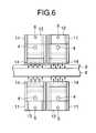
- FIG. 6shows a front view of an EBR head according to the fourth embodiment of the present invention.
- FIG. 7shows a front view of an EBR head according to the fifth embodiment of the present invention.
- FIGS. 8A to 8 Cshows a perspective view to explain the operation according to another embodiment of the present invention.
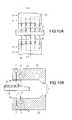
- FIG. 9Ashows a plan view of an EBR head according to the sixth embodiment of the present invention.
- FIG. 9Bshows a cross section taken on line B—B in FIG. 9A;
- FIG. 10Ashows a front view of an EBR head according to a conventional example 1
- FIG. 10Bshows a cross section taken on line C—C in FIG. 10A;
- FIG. 11shows a cross section of an EBR head according to a conventional example 2
- FIG. 12shows a cross section of an EBR head according to a conventional example 3.
- FIG. 13shows a cross section of an EBR head according to a conventional example 4.
- an EBR head 10according to the first embodiment of the present invention is provided in its rear portion with an exhaust 7 and in the upper and lower parts of its front portion with a pair of nozzles, respectively.
- the nozzle closer to the exhaust 7is a slit type chemical rinse nozzle 12 ejecting a rinse chemical 2 in slit form, uniformly onto a glass substrate 8 coated with a resist film 9 .
- the nozzle farther from the exhaust 7is a slit type blow nozzle 14 ejecting a blow gas 1 in slit form, uniformly onto the glass substrate 8 and wider than the ejection effective width of the slit type chemical rinse nozzle 12 .
- the slit type chemical rinse nozzle 12is provided with a chemical supply 5 for supplying the rinse chemical 2 under high pressure by means of a pump or gas through an auto valve 26 supplying and stopping the chemical.
- the slit type blow nozzle 14is provided with a gas supply 4 for supplying the high-pressure blow gas 1 from an auxiliary supply equipment through an auto valve 25 supplying and stopping the gas.
- the rinse chemical 2 and the blow gas 1 ejected from these nozzlesare exhausted from the exhaust 7 .
- the exhaust 7is coupled to exhaust means 231 through an exhaust damper 23 opening and closing exhaust.
- the side of the slit type blow nozzle 14 or the EBR head 10is provided with an EBR sidewall 11 so as to minimize the exhaust opening area for preventing an atmosphere and mist from being leaked.
- a table 21 for mounting the glass substrate 8is provided with a plurality of absorption holes 22 to which vacuum means 241 is connected through the auto valve 24 , which absorbingly hold the glass substrate 8 .
- the width of the slit opening of the slit type nozzledepends on the viscosity of a fluid to be used, but preferably is approximately 0.3 mm or below for a solvent such as a thinner or a chemical such as an alkaline developing solution, and preferably is 0.2 mm or below for gas such as nitrogen gas.
- the chemical rinse nozzle 12 having a slit openingis described.
- a pin type chemical rinse nozzlemay be used instead of the slit type chemical rinse nozzle 12 .
- Japanese Non-examined Patent Publication No. 11-260702there is disclosed that a slit type nozzle can be used as a nozzle ejecting a dissolving agent dissolving a thin film coated onto the substrate of a liquid crystal display.
- the publicationneither discloses a blow nozzle for ejecting high-pressure gas nor suggests that the blow nozzle is of slit type.
- the operation of the embodimentwill be described.
- the EBR heads 10When the EBR heads 10 are in the standby position and the glass substrate 8 coated with the resist film 9 by a spin type coating apparatus is carried to the table 21 by substrate carry means, the auto valve 24 for absorbing the substrate is opened and the glass substrate 8 is absorbingly held to the table 21 through the absorption holes 22 .
- the four EBR heads 10are moved to the position for starting a process of cleaning the end surface, and thereafter the exhaust damper 23 coupled to the exhaust means 231 is opened, starting exhaust in the EBR heads 10 through the exhaust 7 .
- the auto valve 26 for supplying gas coupled to high-pressure gas supply means 261is opened such that the blow gas 1 is supplied through the gas supply 4 to the slit type blow nozzle 14 , thereby starting ejecting gas.
- the auto valve 25 for supplying the chemical coupled to high-pressure rinse chemical supply means 251is opened, the rinse chemical 2 is supplied through the chemical supply 5 to the slit type chemical rinse nozzle 12 , thereby starting ejecting the chemical, and then, the EBR heads 10 are moved in parallel along the perimeter of the glass substrate 8 while performing a process of cleaning the end surface thereof.
- the EBR headsare moved at a speed optionally set with a recipe, a program for the individual apparatuses about a process sequence and control parameters (control target values such as temperature, pressure, gas type, the rate of gas flow, and time) for the respective processing apparatuses, and perform the process a number of reciprocating times optionally set with the recipe likewise, as shown in FIG. 3 .
- the auto valve 25 for supplying the chemicalis closed, thereby stopping the supply of the rinse chemical 2 through the chemical supply 5 to the slit type chemical rinse nozzle 12 .
- the auto valve 26 for supplying gasis closed so as to stop the supply of the blow gas 1 through the gas supply 4 to the slit type blow nozzle 14 .
- the exhaust damper 23is closed so as to stop exhaust in the EBR heads 10 through the exhaust 7 , and thereafter, the EBR heads 10 are moved to the standby position.
- the auto valve 24 for absorbing the substrateis closed so as to release the holding of the glass substrate 8 absorbed to the table 21 , and the glass substrate 8 is carried to the following process by the carrying means.
- the slit type blow nozzle covering a range more widely than the rinse nozzleis used for blowing at high pressure. Even when the slit type nozzle ejects the chemical at high pressure, no mist is scattered to the inside of the substrate, the physical action on the coating film is functioned so as to improve the efficiency. The amount of the liquid used is reduced, and the processing time is reduced.
- FIG. 4is a cross section of an EBR head of assistance in explaining the second embodiment of the present invention.
- the EBR head 10is constructed by integrating the slit type chemical rinse nozzle and the slit type blow nozzle. In other words, the EBR head 10 is provided with a slit type chemical rinse and blow nozzle 15 with a common partition of both nozzles.
- the second embodimenthas the same effect as that of the first embodiment, making it possible to compact the EBR head and to reduce the number of parts.
- FIG. 5is a cross section of an EBR head of assistance in explaining the third embodiment of the present invention.
- the EBR headis of two-fluid construction ejecting a mixture of gas and pure water.
- the EBR headis provided with a slit type chemical rinse and blow nozzle 15 having a single opening with a common slit opening.
- FIG. 6is a front view of an EBR head of assistance in explaining the fourth embodiment of the present invention.
- first EBR unitscomprising the slit type chemical rinse nozzle 12 and the slit type blow nozzle 14
- second EBR unitscomprising a slit type pure water rinse nozzle 13 and the slit type blow nozzle 14 are disposed adjacent each other so as to interpose one side of the glass substrate 8 to be carried.
- an organic alkaline chemical or a mixture of an organic alkaline chemical solventis typically used as the chemical rinse.
- the processrequires pure water rinsing after chemical rinsing.
- the fourth embodimentis of construction of the EBR head 10 by envisaging the case.
- the process of removing a positive resist filmuses an organic solvent as the chemical rinse and will not perform pure water rinsing after chemical rinsing.
- the first to third embodimentsare used for removing a positive resist film.
- FIG. 7is a front view of an EBR head of assistance in explaining the fifth embodiment of the present invention.
- the width of the slit type blow nozzle 14 and the slit type chemical rinse nozzle 12is longer than that of one side of the glass substrate 8 .
- the coating film of the opposed end surface portions of the glass substrate 8is removed; as shown in FIG. 8B, the glass substrate 8 is rotated 90°; and subsequently, as shown in FIG. 8C, the coating film in another opposed end surface portions of the glass substrate 8 can be removed. Accordingly, the processing time for removing a positive resist film can chiefly be reduced as compared with the first to third embodiments and, in particular, there is provided a great effect of shortening tact time in the square substrate for a liquid crystal display that is becoming larger.
- FIGS. 9A and 9Bare a plan view and a cross section of an EBR head of assistance in explaining the sixth embodiment of the present invention.
- the EBR unitscomprising the slit type chemical rinse and blow nozzle 15 and a slit type pure water rinse and blow nozzle 16 are disposed adjacent each other so as to interpose one side of the glass substrate 8 to be carried.
- the width of the respective nozzlesis longer than that of one side of the glass substrate 8 , as in the case of the fifth embodiment.
- the width of the respective nozzlesthat is, the opening length of the slit opening is preferably approximately 10 mm or more longer than the width of one of both sides of the substrate.
- the overall length of the opening lengththerefore, is preferably approximately 20 mm or more longer than the substrate width.
- the sixth embodimentchiefly has the advantage of reducing the processing time for removing a negative resist film, as in the case of the fifth embodiment.
- the slit type blow nozzle covering a range more widely than the slit type rinse nozzleis used for blowing at high pressure. Even when the slit type nozzle ejects the chemical at high pressure, no mist is scattered to the inside of the substrate, the physical action on the coating film is functioned so as to improve the removing efficiency. The amount of the liquid used is reduced, and the processing time is reduced.
- the slit type rinse nozzleejects the chemical at high pressure so as to linearly, uniformly remove the coating film and the removed part section of the coating film is in substantially an isotropic form.
- the slit type blow nozzleis used to blow high-pressure gas so that the liquid of the end surface is blown off and no liquid remains thereon.
- the embodimentsare described by taking the glass substrate as an example.
- the material for the substrate of a display panelis not limited to glass and, needless to say, can be applied to an insulating transparent substrate such as plastic.
Landscapes
- Engineering & Computer Science (AREA)
- Manufacturing & Machinery (AREA)
- Microelectronics & Electronic Packaging (AREA)
- General Physics & Mathematics (AREA)
- Physics & Mathematics (AREA)
- Computer Hardware Design (AREA)
- Condensed Matter Physics & Semiconductors (AREA)
- Power Engineering (AREA)
- Exposure Of Semiconductors, Excluding Electron Or Ion Beam Exposure (AREA)
- Cleaning By Liquid Or Steam (AREA)
- Coating Apparatus (AREA)
- Materials For Photolithography (AREA)
- Application Of Or Painting With Fluid Materials (AREA)
- Cleaning Or Drying Semiconductors (AREA)
Abstract
Description
Claims (16)
Applications Claiming Priority (3)
| Application Number | Priority Date | Filing Date | Title |
|---|---|---|---|
| JP50249/2000 | 2000-02-25 | ||
| JP2000050249AJP3405312B2 (en) | 2000-02-25 | 2000-02-25 | Coating film removal device |
| JP2000-050249 | 2000-02-25 |
Publications (2)
| Publication Number | Publication Date |
|---|---|
| US20010017191A1 US20010017191A1 (en) | 2001-08-30 |
| US6669809B2true US6669809B2 (en) | 2003-12-30 |
Family
ID=18572055
Family Applications (1)
| Application Number | Title | Priority Date | Filing Date |
|---|---|---|---|
| US09/791,793Expired - LifetimeUS6669809B2 (en) | 2000-02-25 | 2001-02-26 | Apparatus for removing a coating film |
Country Status (4)
| Country | Link |
|---|---|
| US (1) | US6669809B2 (en) |
| JP (1) | JP3405312B2 (en) |
| KR (1) | KR100501782B1 (en) |
| TW (1) | TW526520B (en) |
Cited By (12)
| Publication number | Priority date | Publication date | Assignee | Title |
|---|---|---|---|---|
| US20010037858A1 (en)* | 2000-05-08 | 2001-11-08 | Hiroki Taniyama | Processing apparatus, processing system and processing method |
| US20020043275A1 (en)* | 2000-10-13 | 2002-04-18 | Seiichiro Okuda | Substrate processing apparatus |
| US20050026455A1 (en)* | 2003-05-30 | 2005-02-03 | Satomi Hamada | Substrate processing apparatus and substrate processing method |
| US20050056307A1 (en)* | 2003-09-03 | 2005-03-17 | Dainippon Screen Mfg. Co., Ltd. | Substrate cleaning and drying apparatus |
| US20050092351A1 (en)* | 2003-10-30 | 2005-05-05 | Takayuki Saito | Substrate processing apparatus and substrate processing method |
| US20060112979A1 (en)* | 2004-11-30 | 2006-06-01 | Samsung Electronics Co., Ltd. | Nozzle apparatus for stripping edge bead of wafer |
| US20060130968A1 (en)* | 2001-08-02 | 2006-06-22 | Takehiko Orii | Substrate processing apparatus |
| US20070187037A1 (en)* | 2006-02-16 | 2007-08-16 | Choi Dug-Kyu | Semiconductor development apparatus and method using same |
| US20080009142A1 (en)* | 2005-08-10 | 2008-01-10 | International Business Machines Corporation | Evaporation control using coating |
| US20080041523A1 (en)* | 2006-08-01 | 2008-02-21 | Tokyo Electron Limited | Film removing device and film removing method |
| US20090050175A1 (en)* | 2007-08-21 | 2009-02-26 | Takayoshi Tanaka | Substrate cleaning apparatus and substrate cleaning method |
| US20120247670A1 (en)* | 2011-03-31 | 2012-10-04 | Iwatani Corporation | Substrate cleaning apparatus and vacuum processing system |
Families Citing this family (17)
| Publication number | Priority date | Publication date | Assignee | Title |
|---|---|---|---|---|
| JP3944368B2 (en)* | 2001-09-05 | 2007-07-11 | 株式会社荏原製作所 | Substrate processing apparatus and substrate processing method |
| US6936546B2 (en)* | 2002-04-26 | 2005-08-30 | Accretech Usa, Inc. | Apparatus for shaping thin films in the near-edge regions of in-process semiconductor substrates |
| US20080010845A1 (en)* | 2002-04-26 | 2008-01-17 | Accretech Usa, Inc. | Apparatus for cleaning a wafer substrate |
| US20080011421A1 (en)* | 2002-04-26 | 2008-01-17 | Accretech Usa, Inc. | Processing chamber having labyrinth seal |
| KR100954895B1 (en)* | 2003-05-14 | 2010-04-27 | 도쿄엘렉트론가부시키가이샤 | Thin Film Removal Device and Thin Film Removal Method |
| JP2008028156A (en)* | 2006-07-21 | 2008-02-07 | Toppan Printing Co Ltd | Method for removing resist on edge of glass substrate |
| KR100931190B1 (en)* | 2007-12-26 | 2009-12-10 | 주식회사 실트론 | Wafer etching apparatus and wafer processing method using same |
| DE102008045076A1 (en)* | 2008-08-29 | 2010-03-04 | Suss Microtec Lithography Gmbh | Bead removing method for use during processing of substrate i.e. wafer, involves arranging wafer and fluid stream-nozzle relative to each other, and applying fluid stream from nozzle to bead of wafer, where stream has high pressure |
| JP4696165B2 (en)* | 2009-02-03 | 2011-06-08 | 東京エレクトロン株式会社 | Substrate processing apparatus and substrate processing method |
| US8980114B2 (en) | 2011-04-26 | 2015-03-17 | Tazmo Co., Ltd. | Film removing method, nozzle for removing film, and film removing device |
| KR101323911B1 (en)* | 2011-08-30 | 2013-10-30 | 주식회사 케이씨텍 | Method of removing edge bead on substrate and apparatus used therein |
| KR101876191B1 (en)* | 2012-02-10 | 2018-07-09 | 주식회사 케이씨텍 | Substrate treating method and apparatus thereof |
| CN105993061A (en)* | 2014-02-13 | 2016-10-05 | 三菱电机株式会社 | Manufaturing method of semiconductor device |
| JP6780330B2 (en)* | 2015-11-11 | 2020-11-04 | 東京エレクトロン株式会社 | Coating film removing device, coating film removing method and storage medium |
| KR102099433B1 (en)* | 2018-08-29 | 2020-04-10 | 세메스 주식회사 | Apparatus and method of processing stripping a substrate |
| CN111048452A (en)* | 2020-01-03 | 2020-04-21 | 长江存储科技有限责任公司 | Crystal edge etching equipment and crystal edge etching method |
| JP6986781B1 (en)* | 2020-12-25 | 2021-12-22 | 淀川メデック株式会社 | Cleaning table, cleaning device and cleaning method for electronic device laminate |
Citations (8)
| Publication number | Priority date | Publication date | Assignee | Title |
|---|---|---|---|---|
| US4611553A (en)* | 1983-09-12 | 1986-09-16 | Fuji Photo Film Co., Ltd. | Suction nozzle |
| JPH01253923A (en) | 1988-04-01 | 1989-10-11 | Mitsubishi Electric Corp | Coating-film eliminating device |
| US5871584A (en)* | 1994-08-03 | 1999-02-16 | Tokyo Electron Limited | Processing apparatus and processing method |
| JPH11260702A (en) | 1998-03-13 | 1999-09-24 | Advanced Display Inc | Wafer edge cleaning apparatus and manufacture of liquid crystal display apparatus using the apparatus |
| US5997653A (en)* | 1996-10-07 | 1999-12-07 | Tokyo Electron Limited | Method for washing and drying substrates |
| US6114254A (en)* | 1996-10-15 | 2000-09-05 | Micron Technology, Inc. | Method for removing contaminants from a semiconductor wafer |
| JP2001050660A (en)* | 1999-05-31 | 2001-02-23 | Hitachi Electronics Eng Co Ltd | Substrate drying apparatus and drying method |
| US6247479B1 (en)* | 1997-05-27 | 2001-06-19 | Tokyo Electron Limited | Washing/drying process apparatus and washing/drying process method |
Family Cites Families (7)
| Publication number | Priority date | Publication date | Assignee | Title |
|---|---|---|---|---|
| JP2644758B2 (en)* | 1987-07-22 | 1997-08-25 | 株式会社日立製作所 | Resist removal method and apparatus |
| JPH0529210A (en)* | 1991-07-18 | 1993-02-05 | Nec Corp | Method of exfoliating photosensitive resist layer |
| JP2877216B2 (en)* | 1992-10-02 | 1999-03-31 | 東京エレクトロン株式会社 | Cleaning equipment |
| JP3341958B2 (en)* | 1994-08-04 | 2002-11-05 | 東京応化工業株式会社 | Method and apparatus for removing edge coating on substrate |
| JP4127866B2 (en)* | 1996-05-21 | 2008-07-30 | 東京応化工業株式会社 | Method for removing substrate edge coating |
| JPH1187891A (en)* | 1997-09-03 | 1999-03-30 | Ocean:Kk | Equipment for treating printed circuit board |
| JP2000156361A (en)* | 1998-11-20 | 2000-06-06 | Rohm Co Ltd | Method for cleaning semiconductor wafer |
- 2000
- 2000-02-25JPJP2000050249Apatent/JP3405312B2/ennot_activeExpired - Fee Related
- 2001
- 2001-02-22TWTW090104110Apatent/TW526520B/ennot_activeIP Right Cessation
- 2001-02-23KRKR10-2001-0009186Apatent/KR100501782B1/ennot_activeExpired - Fee Related
- 2001-02-26USUS09/791,793patent/US6669809B2/ennot_activeExpired - Lifetime
Patent Citations (8)
| Publication number | Priority date | Publication date | Assignee | Title |
|---|---|---|---|---|
| US4611553A (en)* | 1983-09-12 | 1986-09-16 | Fuji Photo Film Co., Ltd. | Suction nozzle |
| JPH01253923A (en) | 1988-04-01 | 1989-10-11 | Mitsubishi Electric Corp | Coating-film eliminating device |
| US5871584A (en)* | 1994-08-03 | 1999-02-16 | Tokyo Electron Limited | Processing apparatus and processing method |
| US5997653A (en)* | 1996-10-07 | 1999-12-07 | Tokyo Electron Limited | Method for washing and drying substrates |
| US6114254A (en)* | 1996-10-15 | 2000-09-05 | Micron Technology, Inc. | Method for removing contaminants from a semiconductor wafer |
| US6247479B1 (en)* | 1997-05-27 | 2001-06-19 | Tokyo Electron Limited | Washing/drying process apparatus and washing/drying process method |
| JPH11260702A (en) | 1998-03-13 | 1999-09-24 | Advanced Display Inc | Wafer edge cleaning apparatus and manufacture of liquid crystal display apparatus using the apparatus |
| JP2001050660A (en)* | 1999-05-31 | 2001-02-23 | Hitachi Electronics Eng Co Ltd | Substrate drying apparatus and drying method |
Cited By (28)
| Publication number | Priority date | Publication date | Assignee | Title |
|---|---|---|---|---|
| US20010037858A1 (en)* | 2000-05-08 | 2001-11-08 | Hiroki Taniyama | Processing apparatus, processing system and processing method |
| US6827814B2 (en)* | 2000-05-08 | 2004-12-07 | Tokyo Electron Limited | Processing apparatus, processing system and processing method |
| US20020043275A1 (en)* | 2000-10-13 | 2002-04-18 | Seiichiro Okuda | Substrate processing apparatus |
| US6805769B2 (en)* | 2000-10-13 | 2004-10-19 | Dainippon Screen Mfg. Co., Ltd. | Substrate processing apparatus |
| US7862680B2 (en) | 2001-08-02 | 2011-01-04 | Tokyo Electron Limited | Substrate processing apparatus |
| US20060130968A1 (en)* | 2001-08-02 | 2006-06-22 | Takehiko Orii | Substrate processing apparatus |
| US7543593B2 (en)* | 2001-08-02 | 2009-06-09 | Tokyo Electron Limited | Substrate processing apparatus |
| US20080210278A1 (en)* | 2001-08-02 | 2008-09-04 | Takehiko Orii | Substrate processing apparatus |
| US20050026455A1 (en)* | 2003-05-30 | 2005-02-03 | Satomi Hamada | Substrate processing apparatus and substrate processing method |
| US20100043839A1 (en)* | 2003-05-30 | 2010-02-25 | Satomi Hamada | Substrate processing method |
| US20050056307A1 (en)* | 2003-09-03 | 2005-03-17 | Dainippon Screen Mfg. Co., Ltd. | Substrate cleaning and drying apparatus |
| US7415985B2 (en)* | 2003-09-24 | 2008-08-26 | Dainippon Screen Mfg. Co., Ltd. | Substrate cleaning and drying apparatus |
| US20050092351A1 (en)* | 2003-10-30 | 2005-05-05 | Takayuki Saito | Substrate processing apparatus and substrate processing method |
| US7476290B2 (en) | 2003-10-30 | 2009-01-13 | Ebara Corporation | Substrate processing apparatus and substrate processing method |
| US20090090397A1 (en)* | 2003-10-30 | 2009-04-09 | Takayuki Saito | Substrate processing apparatus and substrate processing method |
| US20060112979A1 (en)* | 2004-11-30 | 2006-06-01 | Samsung Electronics Co., Ltd. | Nozzle apparatus for stripping edge bead of wafer |
| US7328713B2 (en)* | 2004-11-30 | 2008-02-12 | Samsung Electronics Co., Ltd. | Nozzle apparatus for stripping edge bead of wafer |
| US20080009142A1 (en)* | 2005-08-10 | 2008-01-10 | International Business Machines Corporation | Evaporation control using coating |
| US20070187037A1 (en)* | 2006-02-16 | 2007-08-16 | Choi Dug-Kyu | Semiconductor development apparatus and method using same |
| US8419891B2 (en)* | 2006-02-16 | 2013-04-16 | Samsung Electronics Co., Ltd. | Semiconductor development apparatus and method using same |
| US8834672B2 (en) | 2006-02-16 | 2014-09-16 | Samsung Electronics Co., Ltd. | Semiconductor development apparatus and method using same |
| US20080041523A1 (en)* | 2006-08-01 | 2008-02-21 | Tokyo Electron Limited | Film removing device and film removing method |
| US8016976B2 (en)* | 2006-08-01 | 2011-09-13 | Tokyo Electron Limited | Film removing device and film removing method |
| US8343284B2 (en) | 2006-08-01 | 2013-01-01 | Tokyo Electron Limited | Film removing device and film removing method |
| US20090050175A1 (en)* | 2007-08-21 | 2009-02-26 | Takayoshi Tanaka | Substrate cleaning apparatus and substrate cleaning method |
| US7958899B2 (en)* | 2007-08-21 | 2011-06-14 | Dainippon Screen Mfg. Co., Ltd. | Substrate cleaning apparatus and substrate cleaning method |
| US20120247670A1 (en)* | 2011-03-31 | 2012-10-04 | Iwatani Corporation | Substrate cleaning apparatus and vacuum processing system |
| US9214364B2 (en)* | 2011-03-31 | 2015-12-15 | Tokyo Electron Limited | Substrate cleaning apparatus and vacuum processing system |
Also Published As
| Publication number | Publication date |
|---|---|
| US20010017191A1 (en) | 2001-08-30 |
| KR20010085514A (en) | 2001-09-07 |
| KR100501782B1 (en) | 2005-07-18 |
| JP2001244169A (en) | 2001-09-07 |
| JP3405312B2 (en) | 2003-05-12 |
| TW526520B (en) | 2003-04-01 |
Similar Documents
| Publication | Publication Date | Title |
|---|---|---|
| US6669809B2 (en) | Apparatus for removing a coating film | |
| JP3892792B2 (en) | Substrate processing apparatus and substrate cleaning apparatus | |
| JP4397299B2 (en) | Substrate processing equipment | |
| JP5016351B2 (en) | Substrate processing system and substrate cleaning apparatus | |
| US7803230B2 (en) | Substrate cleaning apparatus, substrate cleaning method, and medium for recording program used for the method | |
| US11967509B2 (en) | Substrate processing apparatus, substrate processing method, and storage medium | |
| US20070235062A1 (en) | Substrate processing method and substrate processing apparatus | |
| US8147153B2 (en) | Rinsing method, developing method, developing system and computer-read storage medium | |
| KR101437071B1 (en) | Method for removing liquid aerosol particles | |
| JP6512554B2 (en) | Substrate processing method and substrate processing apparatus | |
| TW201719738A (en) | Substrate processing method and substrate processing device | |
| JP2002301413A (en) | Nozzle and coating apparatus | |
| JP4109175B2 (en) | Semiconductor manufacturing equipment | |
| KR20100056993A (en) | Device and method for removing liquid from a surface of a disc-like article | |
| TWI248156B (en) | Cleaning and drying apparatus for substrate holder chuck and method thereof | |
| JP4781253B2 (en) | Substrate processing apparatus and substrate processing method | |
| JPH06196401A (en) | Cleaning apparatus for edge of substrate | |
| KR20070077089A (en) | Application method, application device and storage medium | |
| JPH09232212A (en) | Developing apparatus | |
| TWI856465B (en) | Substrate processing apparatus and substrate processing method | |
| CN118098929A (en) | Substrate processing method, apparatus, computer device, and storage medium | |
| JP2024091022A (en) | SUBSTRATE PROCESSING APPARATUS AND SUBSTRATE PROCESSING METHOD | |
| JP2000323448A (en) | Substrate edge film removing unit and method | |
| KR100513436B1 (en) | Thin film removing apparatus | |
| JP2006051504A (en) | Applicator |
Legal Events
| Date | Code | Title | Description |
|---|---|---|---|
| AS | Assignment | Owner name:NEC CORPORATION, JAPAN Free format text:ASSIGNMENT OF ASSIGNORS INTEREST;ASSIGNORS:HASHIMOTO, YOSHIAKI;SATO, YASUYUKI;REEL/FRAME:011565/0732 Effective date:20010215 | |
| AS | Assignment | Owner name:NEC LCD TECHNOLOGIES, LTD., JAPAN Free format text:ASSIGNMENT OF ASSIGNORS INTEREST;ASSIGNOR:NEC CORPORATION;REEL/FRAME:013649/0828 Effective date:20030401 | |
| FEPP | Fee payment procedure | Free format text:PAYOR NUMBER ASSIGNED (ORIGINAL EVENT CODE: ASPN); ENTITY STATUS OF PATENT OWNER: LARGE ENTITY | |
| STCF | Information on status: patent grant | Free format text:PATENTED CASE | |
| FPAY | Fee payment | Year of fee payment:4 | |
| AS | Assignment | Owner name:NEC CORPORATION,JAPAN Free format text:ASSIGNMENT OF ASSIGNORS INTEREST;ASSIGNOR:NEC LCD TECHNOLOGIES, LTD.;REEL/FRAME:024492/0176 Effective date:20100301 Owner name:NEC CORPORATION, JAPAN Free format text:ASSIGNMENT OF ASSIGNORS INTEREST;ASSIGNOR:NEC LCD TECHNOLOGIES, LTD.;REEL/FRAME:024492/0176 Effective date:20100301 | |
| FEPP | Fee payment procedure | Free format text:PAYOR NUMBER ASSIGNED (ORIGINAL EVENT CODE: ASPN); ENTITY STATUS OF PATENT OWNER: LARGE ENTITY Free format text:PAYER NUMBER DE-ASSIGNED (ORIGINAL EVENT CODE: RMPN); ENTITY STATUS OF PATENT OWNER: LARGE ENTITY | |
| FPAY | Fee payment | Year of fee payment:8 | |
| AS | Assignment | Owner name:GETNER FOUNDATION LLC, DELAWARE Free format text:ASSIGNMENT OF ASSIGNORS INTEREST;ASSIGNOR:NEC CORPORATION;REEL/FRAME:026254/0381 Effective date:20110418 | |
| CC | Certificate of correction | ||
| FPAY | Fee payment | Year of fee payment:12 | |
| AS | Assignment | Owner name:VISTA PEAK VENTURES, LLC, TEXAS Free format text:ASSIGNMENT OF ASSIGNORS INTEREST;ASSIGNOR:GETNER FOUNDATION LLC;REEL/FRAME:045469/0023 Effective date:20180213 | |
| AS | Assignment | Owner name:GETNER FOUNDATION LLC, DELAWARE Free format text:SECURITY INTEREST;ASSIGNOR:VISTA PEAK VENTURES, LLC;REEL/FRAME:060654/0430 Effective date:20180213 |