US6669803B1 - Simultaneous provision of controlled height bonding material at a wafer level and associated structures - Google Patents
Simultaneous provision of controlled height bonding material at a wafer level and associated structuresDownload PDFInfo
- Publication number
- US6669803B1 US6669803B1US09/672,445US67244500AUS6669803B1US 6669803 B1US6669803 B1US 6669803B1US 67244500 AUS67244500 AUS 67244500AUS 6669803 B1US6669803 B1US 6669803B1
- Authority
- US
- United States
- Prior art keywords
- die
- wafer
- dies
- bonding material
- recited
- Prior art date
- Legal status (The legal status is an assumption and is not a legal conclusion. Google has not performed a legal analysis and makes no representation as to the accuracy of the status listed.)
- Expired - Lifetime, expires
Links
Images


Classifications
- H—ELECTRICITY
- H01—ELECTRIC ELEMENTS
- H01L—SEMICONDUCTOR DEVICES NOT COVERED BY CLASS H10
- H01L25/00—Assemblies consisting of a plurality of semiconductor or other solid state devices
- H01L25/16—Assemblies consisting of a plurality of semiconductor or other solid state devices the devices being of types provided for in two or more different subclasses of H10B, H10D, H10F, H10H, H10K or H10N, e.g. forming hybrid circuits
- H01L25/167—Assemblies consisting of a plurality of semiconductor or other solid state devices the devices being of types provided for in two or more different subclasses of H10B, H10D, H10F, H10H, H10K or H10N, e.g. forming hybrid circuits comprising optoelectronic devices, e.g. LED, photodiodes
- G—PHYSICS
- G02—OPTICS
- G02B—OPTICAL ELEMENTS, SYSTEMS OR APPARATUS
- G02B6/00—Light guides; Structural details of arrangements comprising light guides and other optical elements, e.g. couplings
- G02B6/10—Light guides; Structural details of arrangements comprising light guides and other optical elements, e.g. couplings of the optical waveguide type
- G02B6/12—Light guides; Structural details of arrangements comprising light guides and other optical elements, e.g. couplings of the optical waveguide type of the integrated circuit kind
- H—ELECTRICITY
- H10—SEMICONDUCTOR DEVICES; ELECTRIC SOLID-STATE DEVICES NOT OTHERWISE PROVIDED FOR
- H10F—INORGANIC SEMICONDUCTOR DEVICES SENSITIVE TO INFRARED RADIATION, LIGHT, ELECTROMAGNETIC RADIATION OF SHORTER WAVELENGTH OR CORPUSCULAR RADIATION
- H10F39/00—Integrated devices, or assemblies of multiple devices, comprising at least one element covered by group H10F30/00, e.g. radiation detectors comprising photodiode arrays
- H10F39/80—Constructional details of image sensors
- H10F39/806—Optical elements or arrangements associated with the image sensors
- G—PHYSICS
- G02—OPTICS
- G02B—OPTICAL ELEMENTS, SYSTEMS OR APPARATUS
- G02B6/00—Light guides; Structural details of arrangements comprising light guides and other optical elements, e.g. couplings
- G02B6/24—Coupling light guides
- G02B6/42—Coupling light guides with opto-electronic elements
- G02B6/43—Arrangements comprising a plurality of opto-electronic elements and associated optical interconnections
- H—ELECTRICITY
- H01—ELECTRIC ELEMENTS
- H01L—SEMICONDUCTOR DEVICES NOT COVERED BY CLASS H10
- H01L2924/00—Indexing scheme for arrangements or methods for connecting or disconnecting semiconductor or solid-state bodies as covered by H01L24/00
- H01L2924/0001—Technical content checked by a classifier
- H01L2924/0002—Not covered by any one of groups H01L24/00, H01L24/00 and H01L2224/00
- Y—GENERAL TAGGING OF NEW TECHNOLOGICAL DEVELOPMENTS; GENERAL TAGGING OF CROSS-SECTIONAL TECHNOLOGIES SPANNING OVER SEVERAL SECTIONS OF THE IPC; TECHNICAL SUBJECTS COVERED BY FORMER USPC CROSS-REFERENCE ART COLLECTIONS [XRACs] AND DIGESTS
- Y10—TECHNICAL SUBJECTS COVERED BY FORMER USPC
- Y10T—TECHNICAL SUBJECTS COVERED BY FORMER US CLASSIFICATION
- Y10T156/00—Adhesive bonding and miscellaneous chemical manufacture
- Y10T156/10—Methods of surface bonding and/or assembly therefor
- Y10T156/1052—Methods of surface bonding and/or assembly therefor with cutting, punching, tearing or severing
- Y—GENERAL TAGGING OF NEW TECHNOLOGICAL DEVELOPMENTS; GENERAL TAGGING OF CROSS-SECTIONAL TECHNOLOGIES SPANNING OVER SEVERAL SECTIONS OF THE IPC; TECHNICAL SUBJECTS COVERED BY FORMER USPC CROSS-REFERENCE ART COLLECTIONS [XRACs] AND DIGESTS
- Y10—TECHNICAL SUBJECTS COVERED BY FORMER USPC
- Y10T—TECHNICAL SUBJECTS COVERED BY FORMER US CLASSIFICATION
- Y10T156/00—Adhesive bonding and miscellaneous chemical manufacture
- Y10T156/10—Methods of surface bonding and/or assembly therefor
- Y10T156/1089—Methods of surface bonding and/or assembly therefor of discrete laminae to single face of additional lamina
- Y10T156/1092—All laminae planar and face to face
- Y10T156/1093—All laminae planar and face to face with covering of discrete laminae with additional lamina
Definitions
- the present inventionis directed to creating optical systems on a wafer level, including bonding at least two dies together.
- the present inventionis directed efficient creation of optical systems, particularly the efficient provision of bonding material of a controlled height, the final individual module having at least two bonded dies.
- optical elementsis to include passive optical elements, such as diffractive lenses, refractive lenses, beam splitters, rotators, mirrors, i.e., elements which affect light incident thereon, as well as active optical elements, which create light or which have physical characteristics thereof modified in response to light.
- passive optical elementssuch as diffractive lenses, refractive lenses, beam splitters, rotators, mirrors, i.e., elements which affect light incident thereon, as well as active optical elements, which create light or which have physical characteristics thereof modified in response to light.
- passive alignment techniqueshave been used as set forth in U.S. Pat. No. 5,638,469 to Feldman entitled “Microelectronic Module Having Optical and Electrical Interconnects”.
- One such passive alignment techniqueis to place metal pads on the optics and on the laser and place solder between them and use self-alignment properties to achieve the alignment. When solder reflows, surface tension therein causes the parts to self-align.
- passive alignmenthas not been employed for wafer-to-wafer alignment. In particular, the high density of solder bumps required and the thickness and mass of the wafer make such alignment impractical.
- Another problem in wafer level production of optical elements including bonding at least two wafersarises due to the dicing process for forming the individual integrated elements.
- the dicing processis messy due to the use of a dicing slurry.
- the surfaces thereofmay be cleaned to remove the dicing slurry.
- the slurryenters the gap between the wafers. Removing the slurry from the gap formed between the wafers is quite difficult.
- Passive optical elementsthemselves may be formed photolithographically, as set forth, for example, in U.S. Pat. No. 5,218,471 to Swanson et al. entitled “High-efficiency, Multilevel, Diffractive Optical Elements”.
- the passive optical elementsmay also be formed by injection molding, as set forth, for example, in U.S. Pat. No. 5,728,324 to Welch et al. entitled “Molding Diffractive Optical Elements”. Further, the passive optical elements may be made by replicating on a wafer level, as set forth, for example, in U.S. Pat. No. 6,027,595 to Suleski et al.
- FIG. 1 ais a perspective view illustrating wafers to be bonded
- FIG. 1 bis a top view illustrating an individual die on a wafer to be bonded
- FIGS. 2 a - 2 dillustrate a cross section for patterning a bonding material on a wafer
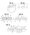
- FIG. 3 ais a top view of a spacer wafer of the present invention.
- FIG. 3 bis a sample cross-section of the spacer wafer of FIG. 3 a;
- FIGS. 4 a - 4 cillustrate specific examples of creating two bonded dies
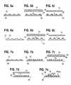
- FIGS. 5 a - 5 cillustrate a method for providing adhesive to a wafer having a plurality of spacers formed thereon and bonding another wafer thereto;
- FIGS. 6 a - 6 cillustrate a method for providing adhesive to a wafer having a plurality of spacers formed therein and bonding another wafer thereto;
- FIGS. 7 a - 7 eillustrate a method for providing adhesive to a plurality of dies having spacers thereon and bonding these dies to another wafer or die;
- FIG. 8is a flow chart of the bonding process of the present invention.
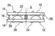
- a first substrate wafer 10 and a second substrate wafer 12are to be bonded together in order to provide integrated optical module.
- a waferis a disc, typically four, six, eight, or twelve inches in diameter and typically having a thickness between 400 microns and 6 mm, and typically made of Si, SiO 2 , GaAs, or any other semiconductor material capable of modulating electromagnetic radiation.
- At least one of these wafershas an array of respective optical elements 19 formed thereon on either one or both surfaces thereof.
- the individual optical elements 19 to be integratedmay consist of one or more optical elements. Further, the optical elements on the wafers may be identical, or may differ from one another.
- both substrates 10 and 12include fiducial marks 18 somewhere thereon, most likely at an outer edge thereof, to ensure alignment of the wafers so that all the individual elements thereon are aligned simultaneously.
- the fiducial marks 18may be used to create mechanical alignment features 18 ′ on the wafers 11 , 12 .
- One or both fiducial marks 18 and the alignment features 18 ′may be used to align the wafers.
- FIG. 1 bshows a top view of a die 1 to be bonded including the location of surrounding bonding material 14 for a particular element 19 .
- the bonding material 14is placed at strategic locations on either substrate in order to facilitate the attachment thereof.
- the bonding material 14is to completely surround the individual optical element 19 .
- the bonding material 14forms a seal between the wafers at these critical junctions. During dicing, the seal prevents dicing slurry and any other dicing by-products, from entering between the elements, which would result in contamination thereof. Since when bonded on a wafer level, the elements remain bonded together, it is nearly impossible to remove any contaminants trapped there between. The dicing contaminants present even more problems when diffractive elements are being created, since the structures of diffractive elements tend to trap the slurry.
- an adhesive or soldercan be used as the bonding material 14 .
- Solderis preferable in many applications because it is smoother than adhesives and allows easier movement prior to bonding.
- Adhesiveshave the advantages of being less expensive for a number of applications, they can be bonded with or without heating, they do not suffer with oxidation, and they can be transparent.
- Viscositydirectly impacts bond thickness, strength, and continuity. Different specific applications will require different bond properties and therefore specific adhesive viscosity.
- FIGS. 2 a - 2 dillustrate an embodiment for allowing accurate control of the height of the bonding material 14 . Only an individual optical element is shown, although the creation occurs on a wafer level.
- a refractive element 20is formed on the wafer 12 on the wafer level.
- the refractive element 20 and the regions adjacent theretoare covered by a bonding material layer 14 ′.
- the bonding material layer 14 ′covers the entire surface of the wafer 12 .
- the bonding material layer 14 ′may be uniformly created using known techniques, e.g., spinning, spraying, dipping or any other methods for uniformly applying the bonding material.
- spacers 15are then provided on the bonding material layer 14 ′ at appropriate portions outside the path of the optical elements 20 .
- the bonding material layer 14 ′is then cured.
- This structure in FIG. 2 cis then subjected to an etching process, e.g., dry or wet etching, to remove the excess bonding material from the areas not covered by the spacers 15 , resulting in the structure shown in FIG. 2 d.
- the spacers 15may then be removed, or may remain to provide a desired gap between the wafer 12 and a wafer to be stacked thereon. If the spacer 15 remains thereon, at least one of the other wafer and a top surface to of the spacer 15 is provided with a bonding material.
- the bonding materialmay only be partially cured, the pattern formed by the spacer 15 removed and then the bonding material brought into contact with the other piece to be bonded thereto. The bonding material would then be fully cured to bond the piece to be integrated.
- the bonding material used in the creation shown in FIGS. 2 a - 2 dis preferably a UV curable adhesive such as polyurethane, epoxy, polyester or acrylic resins.
- a UV curable adhesivesuch as polyurethane, epoxy, polyester or acrylic resins.
- One preferred embodimentuses Norland Optical Adhesive No. 73.
- the spacers 15are preferably also formed on a wafer level and preferably surround respective optical elements. In addition to spacers, the elements used to pattern the bonding material layer may also serve as mechanical structures for facilitating passive alignment with other dies.
- the spacers 15 and the UV curable adhesive layercan be replaced by uniformly applying a mixture of a UV curable resin, such as a bisphenol A novolac glycidyl ether polymer resin and a photoacid generator such as triarylsulfonium salt.
- a UV curable resinsuch as a bisphenol A novolac glycidyl ether polymer resin
- a photoacid generatorsuch as triarylsulfonium salt.
- the bonding material layer containing the novolac glycidyl ether and triarylsulfonium saltmay be uniformly created using known techniques, e.g., spinning, spraying, dipping or any other methods for uniformly applying the bonding material.
- the SU-8 materialis exposed by a mask, which serves to cure the exposed regions photolithographically.
- the unexposed regionsare removed by wet etchingusing solvents such as PGMEA (propylene glycol n) monomethyl ether acetate, a
- a wafer 30includes a plurality of holes 32 therein. Since the wafer 30 is to serve as a mask for the bonding material, the holes 32 are preferably through holes. These holes 32 are to be aligned over the optical elements on the other wafer being processed.
- One way to form a wafer of spacersis to etch, either wet or dry, a silicon wafer.
- etchingoccurs very quickly along the 0,0,1 plane, and very slowly along the 1,1,1 plane of the silicon.
- Etching both sides of the wafer for the same time to etch halfway through either surfaceresults in the cross section shown in FIG. 3 b.
- This particular etchingresults in spacing elements having in a 54° angled surface where etched. Creation of holes in a wafer allows the thickness of the spacers to be easily controlled.
- the wafer shown in FIG. 3 amay also be used to provide bonding material on top of spacers on the wafer being processed or even directly on the wafer being processed itself.
- the holesdo not have to go all the way through the wafer 30 , but only have to be deep enough so that any bonding material applied thereto will not be transferred to the receiving surface.
- the bonding materialmay be uniformly provided on the wafer 30 as discussed above.
- the wafer 30 having the bonding material thereonis then brought into contact with the receiving surface and then the wafer 30 is removed.
- the object to be bonded to the receiving surfaceis then positioned and the bonding material is cured. This technique is particularly useful for providing bonding material on top of spacers, on surfaces receiving dies rather than wafers, and on wafers in which all of the elements are not in the same plane.
- the bonding materialWhen bonding two wafers both having continuous surfaces together or when bonding prior to dicing results in a structure which is difficult to clean, the bonding material preferably completely seals each element to be individually utilized. Thus, when dicing a wafer in order to perform the individual elements, dicing slurry used in the dicing process is prevented from contaminating the optical elements. Thus, in addition to providing a structural component to maintain alignment and rigidity during dicing, the bonding material seal also makes the dicing a much cleaner process for the resultant integrated dies. However, when bonding and dicing a wafer of through holes, such as shown in FIG. 3 b, and a continuous wafer, this seal does not have to be formed, since dicing slurry will enter through the holes and the wafer being processed can be cleaned through the hole before further processing.
- FIG. 4 aA specific example of integrated multiple optical elements is shown in FIG. 4 a.
- a refractive 20is formed on a surface of the first substrate 12 .
- a diffractive 22is formed on a surface of the other substrate 10 .
- a diffractive 28may also be formed on a bottom surface of either substrate.
- the spacers 15have bonding material 14 provided on the top and bottom thereof.
- the fiducial marks 18may also be used to provide metalized pads 24 as shown in FIG. 4 a on opposite sides of the substrates rather than their bonding surfaces in order to facilitate alignment and insertion of the integrated multiple optical element into its intended end use.
- metal padsare particularly useful for mating the integrated multiple optical elements with an active or electrical element, such as in a laser for use in an optical head, a laser pointer, a detector, etc.
- metal 26may be placed on the same surface as the diffractive 22 itself using the fiducial marks 18 , also as shown in FIG. 4 a.
- FIG. 4 billustrates another example of integrated optical module.
- a refractive 20is formed on a surface of the first substrate 12 .
- a laser 25is provided in a bench 17 in the wafer 12 .
- This benchmay be formed by etching silicon.
- a reflective surface 27is also provided to redirect the light from the laser 25 .
- a die 11 containing a diffractive element 22is bonded to the wafer 12 via the bonding material 14 .
- the bondingoccurs prior to dicing.
- the bonding materialmay be provided, the wafer 12 diced, and then the die 11 bonded thereto.
- FIG. 4 cillustrates another example of an integrated optical module.
- a wafer 12 having refractives 20 formed thereon and the wafer 30are bonded together using bonding material 14 .
- the bonded pairmay be diced through the spacing portions 34 to form a refractive 20 with spacers thereon.
- the refractive 20is cleaned after dicing.
- the maskdoes not have to be placed in direct contact with the adhesive material. This is particularly useful when employing an adhesive which has more than one curing mechanism, e.g., thermoset epoxies such as Norland 73 and Masterbond UC 15.
- a maskmay be placed in proximity with the adhesive on a wafer and exposed to UV radiation. The exposed adhesive is then developed with a solvent to remove unwanted portions. Another die/wafer is then aligned with the wafer having the patterned adhesive thereon. The pair is then placed in contact and baked to bond the wafer and the wafer die by thermally cross-linking the adhesive.
- a wafer with an array of spacers formed on the wafer or attached theretomay be contacted with another wafer serving as a transfer wafer having a uniform layer of adhesive thereon. This contact will leave the adhesive on the spacers for facilitating further bonding to a die/wafer. Two examples of this are shown in FIGS. 5 a - 5 c and 6 a - 6 c.
- a wafer 60has a plurality of spacers 63 formed thereon. These spacers may be made of polymer and formed photolithographically on the wafer level.
- a transfer wafer 64 having a uniform layer of bonding material 66is then brought into contact with the wafer 60 .
- the remaining bonding material 68will then be on the top of the spacers 62 . Since the spacers 62 determine where the bonding material will be deposited, the alignment of the wafer 60 and the transfer wafer 64 is not critical. The degree to which the bonding material extends down the side of the spacers 62 will depend on the viscosity of the bonding material and is not of particular importance.
- the two wafersare just raised and lowered relative to one another, without any particular pressure control, as if they were being brought into contact for bonding themselves. The amount of bonding material being transferred depending upon the viscosity of the bonding material, the thickness of the bonding material and the materials of the wafers.
- a second wafer 70may then be aligned and bonded to the wafer 64 .
- FIGS. 6 a - 6 cillustrate a similar method, except here the spacers 74 are formed in the wafer 72 itself, e.g., by etching the wafer 72 .
- the transfer wafer 64 having the uniform layer of bond material 66is brought into contact with and removed from the wafer 72 , leaving bonding material 78 on top of the spacers 74 .
- the second wafer 70may then be aligned and bonded with the wafer 72 .
- FIGS. 7 a - 7 eillustrate a specific example of an alternative to the method of providing the adhesive on a true wafer level.
- the wafer 60has a plurality of spacers 62 thereon.
- This wafer 60is then diced, typically such that each die 82 contains a spacer 62 .
- the dicing of a wafertypically involves the used of a dicing tape 80 .
- the dies 82 remaining of the dicing tape 80may still be simultaneously processed. As shown in FIG.
- the transfer wafer 64 having the uniform layer of bonding material 66 thereonmay be brought into contact with and removed from the spacers simultaneously, leaving bonding material 68 thereon.
- the other wafer 70may be aligned and bonded with the plurality of dies 82 .
- the dicing tape 80is then removed and the bonded structure diced to form the bonded die pair.
- individual dies 84may be aligned with the dies 80 using conventional pick and place techniques and bonded thereto. These die pairs are then simply removed from the dicing tape 80 . The latter method is particularly useful when the dies to be bonded are of different sizes, with the larger dies being on the dicing tape.
- the final production of the die pairis generically referred to as “separating.” While the “separating” will typically be dicing, when the above dicing tape configuration is employed, this separating may include only removing the die pair from the dicing tape.
- FIG. 8shows a flow chart of the general process of bonding in accordance with the present invention.
- bonding materialis patterned on a wafer, either diced or undiced, simultaneously.
- the patterningmay be using a mask, stamping from a spacer wafer, stamping from a transfer wafer, or any of the other techniques used above.
- step 44proceeds to step 46 to determine if the mask is to remain. If the mask remains, whether there is to be further wafer level bonding is determined in step 48 . If not, the die pairs are separated from one another in step 50 , and then cleaned in step 52 .
- step 44proceeds to step 54 , at which a second wafer or a die is aligned to the wafer.
- the bonding materialis cured and the die pairs are separated from one another in step 56 .
- step 46proceeds to step 58 , at which the mask is removed. Then, a second wafer or a die is aligned to the wafer.
- the bonding materialis cured and the die pairs are separated in step 56 . If the mask remains and there is to be further wafer bonding, the step 48 proceeds to step 54 , at which a second wafer or a die is aligned to the wafer.
- the bonding materialis cured and the die pairs are separated in step 56 .
- the elements to be bonded togetherare preferably created by direct photolithographic techniques, as set forth, for example, in U.S. Pat. No. 5,161,059 to Swanson, which is hereby incorporated by reference, for the diffractive optical elements, or in creating the spherical refractive elements by melting a photoresist as taught in O. Wada, “Ion-Beam Etching of InP and its Application to the Fabrication of High Radiance InGAsP/InP Light Emitting Diodes,” General Electric Chemical Society, Solid State Science and Technology, Vol. 131, No.
- these photolithographic techniquesmay be used to make a master element in glass which in turn may then be used to stamp out the desired element on a wafer level in a layer of embossable material as set forth in previously cited U.S. Pat. No. 6,027,595 to Suleski et al. entitled “Method of Making Optical Replicas by Stamping in Photoresist and Replicas Made Thereby”.
Landscapes
- Physics & Mathematics (AREA)
- Engineering & Computer Science (AREA)
- Microelectronics & Electronic Packaging (AREA)
- General Physics & Mathematics (AREA)
- Condensed Matter Physics & Semiconductors (AREA)
- Computer Hardware Design (AREA)
- Power Engineering (AREA)
- Optics & Photonics (AREA)
- Micromachines (AREA)
- Pressure Sensors (AREA)
Abstract
Description
Claims (27)
Priority Applications (3)
| Application Number | Priority Date | Filing Date | Title |
|---|---|---|---|
| US09/672,445US6669803B1 (en) | 1997-10-03 | 2000-09-29 | Simultaneous provision of controlled height bonding material at a wafer level and associated structures |
| AU2001293067AAU2001293067A1 (en) | 2000-09-29 | 2001-09-26 | Method of bonding wafers with controlled height and associated structures |
| PCT/US2001/029955WO2002027363A2 (en) | 2000-09-29 | 2001-09-26 | Method of bonding wafers with controlled height and associated structures |
Applications Claiming Priority (3)
| Application Number | Priority Date | Filing Date | Title |
|---|---|---|---|
| US08/943,274US6096155A (en) | 1996-09-27 | 1997-10-03 | Method of dicing wafer level integrated multiple optical elements |
| US09/514,252US6406583B1 (en) | 1996-09-27 | 2000-02-28 | Wafer level creation of multiple optical elements |
| US09/672,445US6669803B1 (en) | 1997-10-03 | 2000-09-29 | Simultaneous provision of controlled height bonding material at a wafer level and associated structures |
Related Parent Applications (1)
| Application Number | Title | Priority Date | Filing Date |
|---|---|---|---|
| US09/514,252Continuation-In-PartUS6406583B1 (en) | 1996-09-27 | 2000-02-28 | Wafer level creation of multiple optical elements |
Publications (1)
| Publication Number | Publication Date |
|---|---|
| US6669803B1true US6669803B1 (en) | 2003-12-30 |
Family
ID=24698569
Family Applications (1)
| Application Number | Title | Priority Date | Filing Date |
|---|---|---|---|
| US09/672,445Expired - LifetimeUS6669803B1 (en) | 1997-10-03 | 2000-09-29 | Simultaneous provision of controlled height bonding material at a wafer level and associated structures |
Country Status (3)
| Country | Link |
|---|---|
| US (1) | US6669803B1 (en) |
| AU (1) | AU2001293067A1 (en) |
| WO (1) | WO2002027363A2 (en) |
Cited By (20)
| Publication number | Priority date | Publication date | Assignee | Title |
|---|---|---|---|---|
| US20040101987A1 (en)* | 2002-11-22 | 2004-05-27 | Xerox Corporation. | Method of fabrication of electronic devices using microfluidic channels |
| US20050035463A1 (en)* | 2001-03-06 | 2005-02-17 | Digital Optics Corporation | Separating of optical integrated modules and structures formed thereby |
| US20050112298A1 (en)* | 2000-04-26 | 2005-05-26 | Micron Technology, Inc. | Method for making sol gel spacers for flat panel displays |
| US20060125092A1 (en)* | 2000-07-18 | 2006-06-15 | Marshall Paul N | High density integrated circuit package architecture |
| US20060202115A1 (en)* | 2005-03-10 | 2006-09-14 | Hitachi Via Mechanics, Ltd. | Apparatus and method for beam drift compensation |
| US20070236591A1 (en)* | 2006-04-11 | 2007-10-11 | Tam Samuel W | Method for mounting protective covers over image capture devices and devices manufactured thereby |
| US20080180566A1 (en)* | 2007-01-26 | 2008-07-31 | Harpuneet Singh | Wafer level camera module and method of manufacture |
| US20090284837A1 (en)* | 2008-05-13 | 2009-11-19 | Micron Technology, Inc. | Method and apparatus providing uniform separation of lens wafer and structure bonded thereto |
| WO2009141327A1 (en)* | 2008-05-21 | 2009-11-26 | Commissariat A L'energie Atomique | Method of producing an optical device consisting of integrated optoelectronic components |
| US20130122247A1 (en)* | 2011-11-10 | 2013-05-16 | Omnivision Technologies, Inc. | Spacer Wafer For Wafer-Level Camera And Method For Manufacturing Same |
| US8535983B2 (en)* | 2011-06-02 | 2013-09-17 | Infineon Technologies Ag | Method of manufacturing a semiconductor device |
| US8605208B2 (en) | 2007-04-24 | 2013-12-10 | Digitaloptics Corporation | Small form factor modules using wafer level optics with bottom cavity and flip-chip assembly |
| US20140225149A1 (en)* | 2011-09-30 | 2014-08-14 | Osram Opto Semiconductors Gmbh | Optoelectronic Semiconductor Component and Method for Fabricating an Optoelectronic Semiconductor Component |
| US20150204511A1 (en)* | 2012-07-17 | 2015-07-23 | Heptagon Micro Optics Pte. Ltd. | Optical Module, in particular Opto-Electronic Module, and Method of Manufacturing the Same |
| US9419032B2 (en) | 2009-08-14 | 2016-08-16 | Nanchang O-Film Optoelectronics Technology Ltd | Wafer level camera module with molded housing and method of manufacturing |
| US20170309685A1 (en)* | 2014-10-14 | 2017-10-26 | Heptagon Micro Optics Pte. Ltd. | Optical Element Stack Assemblies |
| US10677964B2 (en) | 2017-10-23 | 2020-06-09 | Omnivision Technologies, Inc. | Lens wafer assembly and associated method for manufacturing a stepped spacer wafer |
| US20210057373A1 (en)* | 2019-08-20 | 2021-02-25 | Samsung Electronics Co, Ltd. | Substrate bonding apparatus and method of manufacturing semiconductor device by using the same |
| US11927769B2 (en) | 2022-03-31 | 2024-03-12 | Metalenz, Inc. | Polarization sorting metasurface microlens array device |
| US11978752B2 (en) | 2019-07-26 | 2024-05-07 | Metalenz, Inc. | Aperture-metasurface and hybrid refractive-metasurface imaging systems |
Families Citing this family (3)
| Publication number | Priority date | Publication date | Assignee | Title |
|---|---|---|---|---|
| US6762502B1 (en) | 2000-08-31 | 2004-07-13 | Micron Technology, Inc. | Semiconductor device packages including a plurality of layers substantially encapsulating leads thereof |
| US6921860B2 (en) | 2003-03-18 | 2005-07-26 | Micron Technology, Inc. | Microelectronic component assemblies having exposed contacts |
| US7888758B2 (en) | 2008-03-12 | 2011-02-15 | Aptina Imaging Corporation | Method of forming a permanent carrier and spacer wafer for wafer level optics and associated structure |
Citations (22)
| Publication number | Priority date | Publication date | Assignee | Title |
|---|---|---|---|---|
| US3579816A (en) | 1968-12-23 | 1971-05-25 | Sylvania Electric Prod | Method of producing semiconductor devices |
| US3674004A (en) | 1969-12-30 | 1972-07-04 | Ibm | Precision cutting apparatus and method of operation therefor |
| US3691707A (en) | 1969-11-12 | 1972-09-19 | Sola Basic Ind | Semiconductor material cutting apparatus and method of making the same |
| US3698080A (en) | 1970-11-02 | 1972-10-17 | Gen Electric | Process for forming low impedance ohmic attachments |
| US4523102A (en) | 1980-03-17 | 1985-06-11 | Matsushita Electric Industrial Co., Ltd. | Solid-state color-image sensor and process for fabricating the same |
| US4769108A (en) | 1985-07-06 | 1988-09-06 | Semikron Gesellschaft Fur Gleichrichterbau | System for the production of semiconductor component elements |
| US5034083A (en) | 1989-10-16 | 1991-07-23 | Xerox Corporation | Process and apparatus for assembling smaller scanning or printing arrays together to form an extended array |
| US5049434A (en)* | 1984-04-30 | 1991-09-17 | National Starch And Chemical Investment Holding Corporation | Pre-patterned device substrate device-attach adhesive transfer system |
| US5058997A (en)* | 1989-08-11 | 1991-10-22 | International Business Machines Corporation | Tft lcd with optical interference color filters |
| US5157001A (en) | 1989-09-18 | 1992-10-20 | Matsushita Electric Industrial Co., Ltd. | Method of dicing semiconductor wafer along protective film formed on scribe lines |
| US5182055A (en) | 1988-04-18 | 1993-01-26 | 3D Systems, Inc. | Method of making a three-dimensional object by stereolithography |
| US5214535A (en)* | 1991-12-17 | 1993-05-25 | Xerox Corporation | Lens cover assembly for binary diffractive optic lenses |
| US5482899A (en)* | 1994-03-21 | 1996-01-09 | Texas Instruments Incorporated | Leveling block for semiconductor demounter |
| US5500869A (en) | 1993-03-23 | 1996-03-19 | Mitsubishi Denki Kabushiki Kaisha | Semiconductor laser array device, semiconductor laser device, and production methods therefor |
| EP0731417A2 (en) | 1995-02-27 | 1996-09-11 | Symbol Technologies, Inc. | Scan module for optical scanner |
| US5680702A (en)* | 1994-09-19 | 1997-10-28 | Fuji Xerox Co., Ltd. | Method for manufacturing ink jet heads |
| US5886971A (en) | 1996-09-27 | 1999-03-23 | Digital Optics Corporation | Optical head structures including support substrates adjacent transparent substrates and related methods |
| WO1999018612A2 (en) | 1997-10-03 | 1999-04-15 | Digital Optics Corporation | Wafer level integration of multiple optical elements |
| US6030857A (en)* | 1996-03-11 | 2000-02-29 | Micron Technology, Inc. | Method for application of spray adhesive to a leadframe for chip bonding |
| US6030711A (en)* | 1996-03-11 | 2000-02-29 | Micron Technology, Inc. | Method and apparatus for applying atomized adhesive to a leadframe for chip bonding |
| US6096156A (en)* | 1999-03-11 | 2000-08-01 | Milliken & Company | Vinyl compound plasma pre-treatment for promoting the adhesion between textiles and rubber compounds |
| US6235141B1 (en)* | 1996-09-27 | 2001-05-22 | Digital Optics Corporation | Method of mass producing and packaging integrated optical subsystems |
- 2000
- 2000-09-29USUS09/672,445patent/US6669803B1/ennot_activeExpired - Lifetime
- 2001
- 2001-09-26WOPCT/US2001/029955patent/WO2002027363A2/enactiveApplication Filing
- 2001-09-26AUAU2001293067Apatent/AU2001293067A1/ennot_activeAbandoned
Patent Citations (22)
| Publication number | Priority date | Publication date | Assignee | Title |
|---|---|---|---|---|
| US3579816A (en) | 1968-12-23 | 1971-05-25 | Sylvania Electric Prod | Method of producing semiconductor devices |
| US3691707A (en) | 1969-11-12 | 1972-09-19 | Sola Basic Ind | Semiconductor material cutting apparatus and method of making the same |
| US3674004A (en) | 1969-12-30 | 1972-07-04 | Ibm | Precision cutting apparatus and method of operation therefor |
| US3698080A (en) | 1970-11-02 | 1972-10-17 | Gen Electric | Process for forming low impedance ohmic attachments |
| US4523102A (en) | 1980-03-17 | 1985-06-11 | Matsushita Electric Industrial Co., Ltd. | Solid-state color-image sensor and process for fabricating the same |
| US5049434A (en)* | 1984-04-30 | 1991-09-17 | National Starch And Chemical Investment Holding Corporation | Pre-patterned device substrate device-attach adhesive transfer system |
| US4769108A (en) | 1985-07-06 | 1988-09-06 | Semikron Gesellschaft Fur Gleichrichterbau | System for the production of semiconductor component elements |
| US5182055A (en) | 1988-04-18 | 1993-01-26 | 3D Systems, Inc. | Method of making a three-dimensional object by stereolithography |
| US5058997A (en)* | 1989-08-11 | 1991-10-22 | International Business Machines Corporation | Tft lcd with optical interference color filters |
| US5157001A (en) | 1989-09-18 | 1992-10-20 | Matsushita Electric Industrial Co., Ltd. | Method of dicing semiconductor wafer along protective film formed on scribe lines |
| US5034083A (en) | 1989-10-16 | 1991-07-23 | Xerox Corporation | Process and apparatus for assembling smaller scanning or printing arrays together to form an extended array |
| US5214535A (en)* | 1991-12-17 | 1993-05-25 | Xerox Corporation | Lens cover assembly for binary diffractive optic lenses |
| US5500869A (en) | 1993-03-23 | 1996-03-19 | Mitsubishi Denki Kabushiki Kaisha | Semiconductor laser array device, semiconductor laser device, and production methods therefor |
| US5482899A (en)* | 1994-03-21 | 1996-01-09 | Texas Instruments Incorporated | Leveling block for semiconductor demounter |
| US5680702A (en)* | 1994-09-19 | 1997-10-28 | Fuji Xerox Co., Ltd. | Method for manufacturing ink jet heads |
| EP0731417A2 (en) | 1995-02-27 | 1996-09-11 | Symbol Technologies, Inc. | Scan module for optical scanner |
| US6030857A (en)* | 1996-03-11 | 2000-02-29 | Micron Technology, Inc. | Method for application of spray adhesive to a leadframe for chip bonding |
| US6030711A (en)* | 1996-03-11 | 2000-02-29 | Micron Technology, Inc. | Method and apparatus for applying atomized adhesive to a leadframe for chip bonding |
| US5886971A (en) | 1996-09-27 | 1999-03-23 | Digital Optics Corporation | Optical head structures including support substrates adjacent transparent substrates and related methods |
| US6235141B1 (en)* | 1996-09-27 | 2001-05-22 | Digital Optics Corporation | Method of mass producing and packaging integrated optical subsystems |
| WO1999018612A2 (en) | 1997-10-03 | 1999-04-15 | Digital Optics Corporation | Wafer level integration of multiple optical elements |
| US6096156A (en)* | 1999-03-11 | 2000-08-01 | Milliken & Company | Vinyl compound plasma pre-treatment for promoting the adhesion between textiles and rubber compounds |
Cited By (38)
| Publication number | Priority date | Publication date | Assignee | Title |
|---|---|---|---|---|
| US20050112298A1 (en)* | 2000-04-26 | 2005-05-26 | Micron Technology, Inc. | Method for making sol gel spacers for flat panel displays |
| US20060139561A1 (en)* | 2000-04-26 | 2006-06-29 | Hofmann James J | Mold for forming spacers for flat panel displays |
| US20060125092A1 (en)* | 2000-07-18 | 2006-06-15 | Marshall Paul N | High density integrated circuit package architecture |
| US20050035463A1 (en)* | 2001-03-06 | 2005-02-17 | Digital Optics Corporation | Separating of optical integrated modules and structures formed thereby |
| US7208771B2 (en)* | 2001-03-06 | 2007-04-24 | Digital Optics Corporation | Separating of optical integrated modules and structures formed thereby |
| US20070200132A1 (en)* | 2001-03-06 | 2007-08-30 | Digital Optics Corporation | Electrical connection for optoelectronic devices |
| US20040101987A1 (en)* | 2002-11-22 | 2004-05-27 | Xerox Corporation. | Method of fabrication of electronic devices using microfluidic channels |
| US6872588B2 (en)* | 2002-11-22 | 2005-03-29 | Palo Alto Research Center Inc. | Method of fabrication of electronic devices using microfluidic channels |
| US20060202115A1 (en)* | 2005-03-10 | 2006-09-14 | Hitachi Via Mechanics, Ltd. | Apparatus and method for beam drift compensation |
| US7321114B2 (en)* | 2005-03-10 | 2008-01-22 | Hitachi Via Mechanics, Ltd. | Apparatus and method for beam drift compensation |
| US20070236591A1 (en)* | 2006-04-11 | 2007-10-11 | Tam Samuel W | Method for mounting protective covers over image capture devices and devices manufactured thereby |
| US8456560B2 (en) | 2007-01-26 | 2013-06-04 | Digitaloptics Corporation | Wafer level camera module and method of manufacture |
| US20080180566A1 (en)* | 2007-01-26 | 2008-07-31 | Harpuneet Singh | Wafer level camera module and method of manufacture |
| US8605208B2 (en) | 2007-04-24 | 2013-12-10 | Digitaloptics Corporation | Small form factor modules using wafer level optics with bottom cavity and flip-chip assembly |
| US20090284837A1 (en)* | 2008-05-13 | 2009-11-19 | Micron Technology, Inc. | Method and apparatus providing uniform separation of lens wafer and structure bonded thereto |
| WO2009141327A1 (en)* | 2008-05-21 | 2009-11-26 | Commissariat A L'energie Atomique | Method of producing an optical device consisting of integrated optoelectronic components |
| FR2931587A1 (en)* | 2008-05-21 | 2009-11-27 | Commissariat Energie Atomique | METHOD FOR PRODUCING AN OPTICAL DEVICE WITH INTEGRATED OPTOELECTRONIC COMPONENTS |
| US20110086461A1 (en)* | 2008-05-21 | 2011-04-14 | Commiss. A L'energie Atom. Et Aux Energ. Alterna. | Method for making an optical device with integrated optoelectronic components |
| US8124439B2 (en) | 2008-05-21 | 2012-02-28 | Commissariat A L'energie Atomique Et Aux Energies Alternatives | Method for making an optical device with integrated optoelectronic components |
| US9419032B2 (en) | 2009-08-14 | 2016-08-16 | Nanchang O-Film Optoelectronics Technology Ltd | Wafer level camera module with molded housing and method of manufacturing |
| US8535983B2 (en)* | 2011-06-02 | 2013-09-17 | Infineon Technologies Ag | Method of manufacturing a semiconductor device |
| US20140225149A1 (en)* | 2011-09-30 | 2014-08-14 | Osram Opto Semiconductors Gmbh | Optoelectronic Semiconductor Component and Method for Fabricating an Optoelectronic Semiconductor Component |
| US9324920B2 (en)* | 2011-09-30 | 2016-04-26 | Osram Opto Semiconductors Gmbh | Optoelectronic semiconductor component having a transparent oxide connector and method for fabricating the same |
| US20130122247A1 (en)* | 2011-11-10 | 2013-05-16 | Omnivision Technologies, Inc. | Spacer Wafer For Wafer-Level Camera And Method For Manufacturing Same |
| US10359609B2 (en) | 2011-11-10 | 2019-07-23 | Omnivision Technologies, Inc. | Spacer wafer for wafer-level camera and method for manufacturing same |
| US20150204511A1 (en)* | 2012-07-17 | 2015-07-23 | Heptagon Micro Optics Pte. Ltd. | Optical Module, in particular Opto-Electronic Module, and Method of Manufacturing the Same |
| US10180235B2 (en)* | 2012-07-17 | 2019-01-15 | Heptagon Micro Optics Pte. Ltd. | Optical module, in particular opto-electronic module, and method of manufacturing the same |
| US10741613B2 (en)* | 2014-10-14 | 2020-08-11 | Ams Sensors Singapore Pte. Ltd. | Optical element stack assemblies |
| US20170309685A1 (en)* | 2014-10-14 | 2017-10-26 | Heptagon Micro Optics Pte. Ltd. | Optical Element Stack Assemblies |
| US10677964B2 (en) | 2017-10-23 | 2020-06-09 | Omnivision Technologies, Inc. | Lens wafer assembly and associated method for manufacturing a stepped spacer wafer |
| US11978752B2 (en) | 2019-07-26 | 2024-05-07 | Metalenz, Inc. | Aperture-metasurface and hybrid refractive-metasurface imaging systems |
| US12389700B2 (en) | 2019-07-26 | 2025-08-12 | Metalenz, Inc. | Aperture-metasurface and hybrid refractive-metasurface imaging systems |
| US20210057373A1 (en)* | 2019-08-20 | 2021-02-25 | Samsung Electronics Co, Ltd. | Substrate bonding apparatus and method of manufacturing semiconductor device by using the same |
| US11990444B2 (en)* | 2019-08-20 | 2024-05-21 | Samsung Electronics Co., Ltd. | Substrate bonding apparatus and method of manufacturing semiconductor device by using the same |
| US12224262B2 (en) | 2019-08-20 | 2025-02-11 | Samsung Electronics Co., Ltd. | Substrate bonding apparatus and method of manufacturing semiconductor device by using the same |
| US11927769B2 (en) | 2022-03-31 | 2024-03-12 | Metalenz, Inc. | Polarization sorting metasurface microlens array device |
| WO2024205646A2 (en) | 2022-03-31 | 2024-10-03 | Metalenz, Inc. | Polarization sorting metasurface microlens array device |
| US12276807B2 (en) | 2022-03-31 | 2025-04-15 | Metalenz, Inc. | Polarization sorting metasurface microlens array device |
Also Published As
| Publication number | Publication date |
|---|---|
| AU2001293067A1 (en) | 2002-04-08 |
| WO2002027363A2 (en) | 2002-04-04 |
| WO2002027363A3 (en) | 2003-08-07 |
Similar Documents
| Publication | Publication Date | Title |
|---|---|---|
| US6669803B1 (en) | Simultaneous provision of controlled height bonding material at a wafer level and associated structures | |
| US6649008B2 (en) | Method of mass producing and packaging integrated subsystems | |
| EP1036415B1 (en) | Wafer level integration of multiple optical elements | |
| US6744109B2 (en) | Glass attachment over micro-lens arrays | |
| US20080136955A1 (en) | Integrated camera and associated methods | |
| US8153957B2 (en) | Integrated optical imaging systems including an interior space between opposing substrates and associated methods | |
| US6870259B2 (en) | Wafer scale fiber optic termination | |
| US20060226576A1 (en) | Microstructure devices and their production | |
| JP2004524679A (en) | Light emitting semiconductor package | |
| JP2002100758A (en) | Device including functional block, method of manufacturing the same, and optical transmission device | |
| EP3341974B1 (en) | Optical assemblies including a spacer adhering directly to a substrate | |
| JPH11307878A (en) | Manufacturing method of optical input / output element array device | |
| US8934745B2 (en) | Apparatus for use in optoelectronics having a sandwiched lens | |
| US20070110361A1 (en) | Wafer level integration of multiple optical elements | |
| US11101617B2 (en) | Wafer-level handle replacement | |
| CA2492335C (en) | Wafer level integration of multiple optical elements | |
| AU2004202260B2 (en) | Encapsulated fiber optic terminations | |
| AU2002218872A1 (en) | Wafer scale fiber optic termination |
Legal Events
| Date | Code | Title | Description |
|---|---|---|---|
| AS | Assignment | Owner name:DIGITAL OPTICS CORPORATION, NORTH CAROLINA Free format text:ASSIGNMENT OF ASSIGNORS INTEREST;ASSIGNORS:KATHMAN, ALAN D.;MILLER, HARRIS R.;MATHEWS, JAY;AND OTHERS;REEL/FRAME:011448/0093;SIGNING DATES FROM 20001121 TO 20001128 | |
| STCF | Information on status: patent grant | Free format text:PATENTED CASE | |
| REMI | Maintenance fee reminder mailed | ||
| FEPP | Fee payment procedure | Free format text:PAT HOLDER NO LONGER CLAIMS SMALL ENTITY STATUS, ENTITY STATUS SET TO UNDISCOUNTED (ORIGINAL EVENT CODE: STOL); ENTITY STATUS OF PATENT OWNER: LARGE ENTITY | |
| FPAY | Fee payment | Year of fee payment:4 | |
| SULP | Surcharge for late payment | ||
| AS | Assignment | Owner name:TESSERA NORTH AMERICA, INC., NORTH CAROLINA Free format text:CHANGE OF NAME;ASSIGNOR:DIGITAL OPTICS CORPORATION;REEL/FRAME:021194/0986 Effective date:20070330 | |
| REMI | Maintenance fee reminder mailed | ||
| FPAY | Fee payment | Year of fee payment:8 | |
| SULP | Surcharge for late payment | Year of fee payment:7 | |
| AS | Assignment | Owner name:DIGITALOPTICS CORPORATION EAST, NORTH CAROLINA Free format text:CHANGE OF NAME;ASSIGNOR:TESSERA NORTH AMERICA, INC.;REEL/FRAME:027768/0541 Effective date:20110701 | |
| CC | Certificate of correction | ||
| AS | Assignment | Owner name:FLIR SYSTEMS TRADING BELGIUM BVBA, BELGIUM Free format text:ASSIGNMENT OF ASSIGNORS INTEREST;ASSIGNOR:DIGITALOPTICS CORPORATION EAST;REEL/FRAME:032827/0362 Effective date:20130808 | |
| FPAY | Fee payment | Year of fee payment:12 | |
| AS | Assignment | Owner name:AVAGO TECHNOLOGIES GENERAL IP (SINGAPORE) PTE. LTD Free format text:ASSIGNMENT OF ASSIGNORS INTEREST;ASSIGNOR:FLIR SYSTEMS TRADING BELGIUM BVBA;REEL/FRAME:036126/0092 Effective date:20140827 | |
| AS | Assignment | Owner name:DIGITALOPTICS CORPORATION EAST, NORTH CAROLINA Free format text:CORRECTIVE ASSIGNMENT TO CORRECT THE PATENT NO. 7817833 PREVIOUSLY RECORDED AT REEL: 027768 FRAME: 0541. ASSIGNOR(S) HEREBY CONFIRMS THE ASSIGNMENT;ASSIGNOR:TESSERA NORTH AMERICA, INC.;REEL/FRAME:036733/0896 Effective date:20110701 | |
| AS | Assignment | Owner name:BANK OF AMERICA, N.A., AS COLLATERAL AGENT, NORTH CAROLINA Free format text:PATENT SECURITY AGREEMENT;ASSIGNOR:AVAGO TECHNOLOGIES GENERAL IP (SINGAPORE) PTE. LTD.;REEL/FRAME:037808/0001 Effective date:20160201 Owner name:BANK OF AMERICA, N.A., AS COLLATERAL AGENT, NORTH Free format text:PATENT SECURITY AGREEMENT;ASSIGNOR:AVAGO TECHNOLOGIES GENERAL IP (SINGAPORE) PTE. LTD.;REEL/FRAME:037808/0001 Effective date:20160201 | |
| AS | Assignment | Owner name:AVAGO TECHNOLOGIES GENERAL IP (SINGAPORE) PTE. LTD., SINGAPORE Free format text:TERMINATION AND RELEASE OF SECURITY INTEREST IN PATENTS;ASSIGNOR:BANK OF AMERICA, N.A., AS COLLATERAL AGENT;REEL/FRAME:041710/0001 Effective date:20170119 Owner name:AVAGO TECHNOLOGIES GENERAL IP (SINGAPORE) PTE. LTD Free format text:TERMINATION AND RELEASE OF SECURITY INTEREST IN PATENTS;ASSIGNOR:BANK OF AMERICA, N.A., AS COLLATERAL AGENT;REEL/FRAME:041710/0001 Effective date:20170119 |