US6665232B2 - Synchronous mirror delay with reduced delay line taps - Google Patents
Synchronous mirror delay with reduced delay line tapsDownload PDFInfo
- Publication number
- US6665232B2 US6665232B2US10/369,994US36999403AUS6665232B2US 6665232 B2US6665232 B2US 6665232B2US 36999403 AUS36999403 AUS 36999403AUS 6665232 B2US6665232 B2US 6665232B2
- Authority
- US
- United States
- Prior art keywords
- delay
- coupled
- smd
- circuit
- clock
- Prior art date
- Legal status (The legal status is an assumption and is not a legal conclusion. Google has not performed a legal analysis and makes no representation as to the accuracy of the status listed.)
- Expired - Lifetime
Links
Images


Classifications
- G—PHYSICS
- G11—INFORMATION STORAGE
- G11C—STATIC STORES
- G11C7/00—Arrangements for writing information into, or reading information out from, a digital store
- G11C7/10—Input/output [I/O] data interface arrangements, e.g. I/O data control circuits, I/O data buffers
- G11C7/1051—Data output circuits, e.g. read-out amplifiers, data output buffers, data output registers, data output level conversion circuits
- G11C7/1066—Output synchronization
- G—PHYSICS
- G11—INFORMATION STORAGE
- G11C—STATIC STORES
- G11C7/00—Arrangements for writing information into, or reading information out from, a digital store
- G11C7/10—Input/output [I/O] data interface arrangements, e.g. I/O data control circuits, I/O data buffers
- G11C7/1072—Input/output [I/O] data interface arrangements, e.g. I/O data control circuits, I/O data buffers for memories with random access ports synchronised on clock signal pulse trains, e.g. synchronous memories, self timed memories
- G—PHYSICS
- G11—INFORMATION STORAGE
- G11C—STATIC STORES
- G11C7/00—Arrangements for writing information into, or reading information out from, a digital store
- G11C7/22—Read-write [R-W] timing or clocking circuits; Read-write [R-W] control signal generators or management
- G—PHYSICS
- G11—INFORMATION STORAGE
- G11C—STATIC STORES
- G11C7/00—Arrangements for writing information into, or reading information out from, a digital store
- G11C7/22—Read-write [R-W] timing or clocking circuits; Read-write [R-W] control signal generators or management
- G11C7/222—Clock generating, synchronizing or distributing circuits within memory device
Definitions
- the inventionrelates to integrated circuits, and more particularly, to synchronous mirror delay circuits with delay, line taps for double data rate (DDR) synchronous dynamic random access memory (SDRAM) devices.
- DDRdouble data rate
- SDRAMsynchronous dynamic random access memory
- DRAMdynamic random access memory
- SDRAMsare designed to operate synchronously with the system clock with input and output data synchronized to an active edge of the system clock which is driving the processor accessing the SDRAM.
- DDR SDRAMshave overcome some of the timing disadvantages of other memory devices memory, access is still a limiting factor, and there is a need for still faster memory devices.
- double data rate (DDR) SDRAMswere developed to allow data transfers on both the rising and falling edges of the system data clock, providing twice the operating speed of the conventional SDRAM.
- DDR SDRAMprovides up to twice as much data bandwidth as the conventional SDRAM for a given data clock.
- DDR SDRAMsare also capable of providing bursts of data at a high-speed data rate.
- DDR SDRAMsuse a data strobe signal (DQS) 100 to register the data (DQ) 104 on both edges of the system clock 102 .
- DQSdata strobe signal
- Thisallows the receiving system to improve latching the presented data under the timing constraints of modern high speed memory data transfers.
- the DQShas a known latency 106 , 108 which varies between 3 ⁇ 4 of the system clock cycle (minimum latency) to ⁇ fraction (5/4) ⁇ of the clock cycle (maximum latency).
- DDR SDRAMsutilize a clock skew adjustment circuit to drive this latency variability to as close to zero as feasible and synchronize the DQS signal and output data signals to the system data clock.
- a common clock skew adjustment circuit utilized in DDR SDRAMis a delay locked loop (DLL), shown in FIG. 2 .
- DLL'sgenerally consist of a delay line 200 of individual delay elements, that generates a replica of a clock signal which is compared against the input clock signal.
- the clock signal loaded into the delay line 200is iteratively adjusted until a match or “lock” is achieved.
- the delay line 200is coupled to a shift register 202 that loads data into the delay line 200 to begin generation of the clock pulse signal.
- the individual delay elements (not shown) in the delay linetypically comprise NAND gates that are coupled to an inverter.
- the shift register 202is adjusted by a phase detector 204 that compares the replicated clock pulse against the external clock pulse.
- the phase detector 204increments or decrements the shift register 202 a fixed amount up and down for each clock cycle, allowing the DLL to iterate until a “lock” with the input external clock signal is attained.
- the phase detector 204increments or decrements the shift register 202 a fixed amount up and down for each clock cycle, allowing the DLL to iterate until a “lock” with the input external clock signal is attained.
- a SMD circuitcan attain a lock with the external clock signal in as few as two clock cycles. This ability greatly decreases the time to first access when a DDR SDRAM comes out of a low power mode.
- a SMD circuitgenerally includes two delay lines and an accompanying control circuit, all of which must be of a length sufficient to accommodate the full time period of the clock pulse to be matched. Any additional space that would be required to allow an adequate adjustment range of the clock period must also be incorporated into the SMD circuit, further increasing the SMD circuit size. Therefore, an SMD circuit generally requires more space to implement on the integrated circuit.
- an SMD circuitcomprises a clock source, a delay segment coupled to the clock source, a data path model coupled to the delay segment, a forward delay line coupled to the data path model, an SMD control circuit coupled to the forward delay line and coupled to the clock source, and a backward delay line coupled to the SMD control circuit and coupled to the delay segment.
- an SMD circuitcomprises a clock source, a data path model coupled to the clock source, a first delay segment coupled to the data path model, a forward delay line coupled to the first delay segment, an SMD control circuit coupled to the forward delay line and to the clock source, and a backward delay line coupled to the SMD control circuit, the clock source, and to a second delay segment.
- an integrated circuitcomprises a clock input buffer coupled to receive a clock signal with a time period, a delay segment coupled to the clock input buffer, a data path model coupled to the delay segment, a forward delay line coupled to the data path model, an SMD control circuit coupled to the forward delay line and to the clock input buffer, and a backward delay line coupled to the SMD control circuit and coupled to the delay segment.
- a memory devicecomprises an address interface, a data interface, a control interface, and an SMD clock recovery and skew adjustment circuit.
- the SMD clock recovery and skew adjustment circuitcomprises a clock source, a delay segment coupled to the clock source, a data path model coupled to the delay segment, a forward delay line coupled to the data path model, an SMD control circuit coupled to the forward delay line and coupled to the clock source, and a backward delay line coupled to the SMD control circuit and coupled to the delay segment.
- a DDR memory device interface circuitcomprises a data interface, a DQS signal interface, a data latch coupled to the data interface, and an SMD clock recovery and skew adjustment circuit coupled to the data latch and coupled to the DQS signal interface.
- the SMD clock recovery and skew adjustment circuitcomprises a clock input buffer coupled to receive a clock signal with a time period, a data path model coupled to the clock input buffer, a first delay segment coupled to the data path model, a forward delay line coupled to the first delay segment, an SMD control circuit coupled to the forward delay line and to the clock input buffer, and a backward delay line coupled to the SMD control circuit, the clock input buffer, and to a second delay segment.
- a method of synchronizing with a clock signalcomprises receiving a clock signal having a clock signal time period, subtracting a first time period equivalent to a real data path, subtracting a second time period that is a static component, measuring a remaining component of the clock signal time period, reproducing the remaining component of the clock signal time period, and adding a third time period that is identical to the second time period to the reproduced remaining component of the clock signal time period.
- Another method of synchronizing with a clock signalcomprises receiving a clock signal having a sequential first and second clock signal time period, delaying the first clock signal time period a first time delay, delaying the first clock signal time period a second time delay equal to a real data path, measuring a remaining component of the first clock signal time period, delaying the second clock signal time period the first time delay, reproducing the remaining component of the first clock signal time period, and merging the reproduced remaining component of the clock signal time period to the delayed second clock signal time period.
- a further method of synchronizing with a clock signalcomprises coupling a delay segment to a clock source, coupling a data path model to the delay segment, coupling a forward delay line to the data path model, coupling an SMD control circuit to the forward delay line and to the clock source, and coupling a backward delay line to the SMD control circuit and to the delay segment.
- In yet another method of synchronizing with a clock sourcecomprises coupling a data path model to a clock source, coupling a first delay segment to the data path model, coupling a forward delay line to the first delay segment, coupling an SMD control circuit to the forward delay line and to the clock source, and coupling a backward delay line to the SMD control circuit, the clock source, and to a second delay segment.
- a further method of synchronizing a memory device with a clock sourcecomprises forming an address interface, forming a data interface, forming a control interface, and forming an SMD clock recovery and skew adjustment circuit.
- the SMD clock recovery and skew adjustment circuitcomprises coupling a clock input buffer to receive a clock signal coupling a data path model to the clock input buffer, coupling a first delay segment to the data path model, coupling a forward delay line to the first delay segment, coupling an SMD control circuit to the forward delay line and to the clock input buffer, and coupling a backward delay line to the SMD control circuit, the clock input buffer and to a second delay segment.
- Another method for synchronizing a DDR memory device interface circuit with a clock sourcecomprises forming a data interface, forming a DQS signal interface, forming a data latch coupled to the data interface, and forming an SMD clock recovery and skew adjustment circuit coupled to the data latch and the DQS signal interface.
- the SMD clock recovery and skew adjustment circuitcomprises, a clock source, a delay segment coupled to the clock source, a data path model coupled to the delay segment, a forward delay line coupled to the data path model, an SMD control circuit coupled to the forward delay line and to the clock source, and a backward delay line coupled to the SMD control circuit and coupled to the delay segment.
- FIG. 1is a wave diagram of a DDR SDRAM memory transfer showing the system clock signal, data signal (DQ), and DQS strobe.
- FIG. 2is a diagram of a prior art DLL for an integrated circuit.
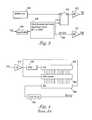
- FIG. 3is a diagram of a DDR SDRAM memory data interface circuit showing DRAM core, data latch, clock recovery circuit, and DQS output.
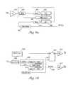
- FIG. 4is a diagram of a prior art SMD circuit.
- FIG. 5is a diagram of an SMD circuit.
- FIG. 6 ais detailed diagrams of a FDL, SMD control, and BDL modules for an SMD circuit.
- FIGS. 6 b and 6 care detailed diagrams of a FDL, a latch based SMD control, and BDL modules for a SMD circuit.
- FIG. 7 ais a diagram of a NAND delay element and inverter.
- FIG. 7 bis a diagram of a two NAND delay element.
- FIG. 8is a diagram of a RC delay element, showing resistor, capacitor and inverter.
- FIGS. 9 a and 9 bare diagrams of an SMD circuit with embodiments of the present invention.
- FIG. 10is a diagram of a DDR SDRAM memory data output circuit showing DRAM core, data latch, SMD clock recovery circuit, and DQS output.
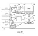
- FIG. 11is a diagram of a memory with an SMD clock recovery circuit.
- FIG. 3shows a generalized data interface of a DDR SDRAM memory, including a DRAM core 300 , a data latch 302 , and a generalized clock recovery and skew adjustment circuit 304 .
- an external data clockis received through the clock input buffer 306 .
- the external data clockis replicated and adjusted for skew by the clock recovery and skew adjustment circuit 304 and output as an internal clock signal 308 .
- the internal clock signal 308is utilized to trigger the data latch 302 on both the rising and falling edge of the clock, outputting data through buffer 310 onto the data bus.
- the internal clock signalis also utilized to drive the DQS strobe through buffer 312 .
- FIG. 4shows an example of a prior art SMD circuit which consists of a clock input buffer 410 , a data path model (DPM) 400 , forward delay line (FDL) 402 , an SMD control circuit 404 , a backward delay line (BDL) 406 , and a clock driver circuit 408 .
- the FDL 402 and BDL 406are comprised of delay elements (not shown) that have the same unit delay.
- the input buffer 410 and clock driver 408adds an additional internal delay for the SMD circuit of d in for the input buffer 410 and delay of d dp for the clock driver circuit 408 to the circuit that is compensated for by the DPM 400 .
- the SMD circuitreceives an external clock signal through the input buffer 410 , which couples the received clock signal to the SMD control 404 , the DPM 400 , and the BDL 406 .
- the received clock signalis passed through the DPM circuit 400 , which has a delay of d in +d dp , replicating the delays of input buffer 410 and clock driver 408 in order to account for them in the recovery of the clock signal.
- the clock signalis then passed to the forward delay line (FDL) 402 , where it is passed sequentially from delay element to delay element.
- the combined delay of the DPM 400 and the FDL 402is such that the forward edge of the received clock signal is still within the FDL 402 when the next external clock signal is received at the input buffer 410 .
- the input buffer 410Upon receiving the next external clock signal the input buffer 410 again couples it to the SMD control 404 and the DPM 400 circuits.
- the next external clock signalenters the DPM circuit 400 and the FDL 402 chain to become the basis of the next recovered clock signal.
- the next external clock signalalso triggers the SMD control 404 , which transfers the current clock signal from the position it has attained in the FDL 402 delay chain to the same position in the BDL 406 delay chain.
- the initial clock signalthen flows backwards through the BDL 406 , which is the same length as the FDL 402 and composed of the same unit delay elements.
- the clock signalwill take the same amount of time to transition through it and will therefore exactly replicate the input clock signal.
- the additional delay factors of the input buffer 410 and clock driver 408will already be taken into account in the clock signal loaded into the BDL 406 by the pre-delay of the DPM 400 , that effectively subtracts the delay factors from the time period measured by the FDL 402 .
- the recovered and skew adjusted clock signalis coupled from the BDL 406 , through the clock driver circuit 408 , to provide a synchronous clock for the circuit that the SMD circuit of FIG. 4 is implemented into.
- FIG. 5shows an example of a SMD circuit which consists of a clock input buffer 510 , a data path model (DPM) 500 , forward delay line (FDL) 502 , a SMD control circuit 504 , a backward delay line (BDL) 506 , and the real data path (RDP) element 508 .
- the RDP 508symbolically represents the real data path circuitry delay added by internal circuitry of the system, such as clock drivers and other logic delays, that the SMD circuit of FIG. 5 is implemented into and is not a real circuit component.
- the FDL 502 and BDL 506are comprised of delay elements (not shown) that have the same unit delay.
- the input buffer 510 and real data path 508add additional internal delays for the SMD circuit, d in for the input buffer 510 and delay of d dp for the RDP 508 , that are compensated for by the DPM 500 .
- the SMD circuitreceives an external clock signal through the input buffer 510 , which couples the received clock signal to the SMD control 504 and the DPM 500 .
- the received clock signalis passed through the DPM circuit 500 , which has a delay of d in +d dp , replicating the delays of input buffer 510 and real data path 508 in order to account for them in the recovery of the clock signal.
- the clock signalis then passed to the forward delay line (FDL) 502 , where it is passed sequentially from delay element to delay element.
- the combined delay of the DPM 500 and the FDL 502is such that the forward edge of the received clock signal is still within the FDL 502 when the next external clock signal is received at the input buffer 510 .
- the input buffer 510Upon receiving the next external clock signal the input buffer 510 again couples it to the SMD control 504 and the DPM 500 circuits.
- the next external clock signalenters the DPM circuit 500 and the FDL 502 chain to become the basis of the next recovered clock signal.
- the next external clock signalalso triggers the SMD control 504 , which transfers the current clock signal from the position it has attained in the FDL 502 delay chain to the same position in the BDL 506 delay chain.
- the next external clock signalenables the BDL 506 and the initial clock signal then flows backwards through the BDL 506 , which is the same length as the FDL 502 and composed of the same unit delay elements.
- the clock signalwill take the same amount of time to transition through it and will therefore exactly replicate the input clock signal.
- the additional delay factors of the input buffer 510 and clock driver 508will already be taken into account in the clock signal loaded into the BDL 506 by the pre-delay of the DPM 500 , that effectively subtracts the delay factors from the time period measured by the FDL 502 .
- the recovered and skew adjusted clock signalis coupled from the BDL 506 to provide a synchronous clock for the circuit that the SMD circuit of FIG. 5 is implemented into, the delay of which is represented by the real data path 508 .
- FIGS. 7 a and 7 bShown in FIGS. 7 a and 7 b are examples of NAND delay elements, such as would typically be used in either the FDL or the BDL of SMD circuits.
- the delay element in FIG. 7 acomprises a NAND gate 700 coupled to an inverter 702 .
- the delay element in FIG. 7 bcomprises a first NAND gate 704 coupled to a second NAND gate 706 . Additional delay element structures or gate delays that could be utilized, such as, skew limited delays, and etc., will be apparent to those skilled in the art with the benefit of the present specification.
- FIGS. 6 a and 6 bare expanded example views of the FDL 600 , SMD control 602 , and BDL 604 of a SMD circuit, to show circuit elements and interconnections. It is understood that the SMD circuits of FIGS. 6 a and 6 b work in conjunction with the other components that further comprise the SMD circuit such as shown in FIGS. 4 and 5.
- the FDL 600includes a coupled series of such NAND delay elements, 606 , 608 , and 610 .
- a clock signalenters the FDL 600 on input 612 and is coupled to the NAND gate of the first delay element 606 , where the other input is coupled to Vcc.
- the signalpasses through the first delay element 606 and is coupled to the next series delay element 608 , which also has its unused input tied to Vcc.
- the input clock signalis passed in this manner through the FDL 602 until the final delay element 610 is reached. As shown in FIG.
- each delay element, 606 , 608 , and 610is coupled, 614 , 616 , and 618 , to an input of the SMD control 602 .
- the SMD control 602consists of a sequence of NAND gates, 620 , 622 , and 624 , that each have an input coupled to a control input 626 that generally accepts a clock signal.
- the other input to the NAND gates, 620 , 622 , and 624 , of the SMD control 602is coupled to an input, 614 , 616 , and 618 , respectively, from the FDL 600 .
- the outputs of NAND gates, 620 , 622 , and 624is coupled, 628 , 630 , and 632 , to inputs of the series coupled delay elements, 634 , 636 , and 638 , that are incorporated into the BDL 604 .
- the current clock signal that is transitioning the FDL 600 delay element chainis transferred through the SMD control 602 to the same position in the BDL 604 delay element chain.
- the delay elements, 634 , 636 , and 638 , of the BDL 604are coupled in series, but flow in an opposite direction from the FDL 600 delay element chain.
- An input of the initial element 638 in the BDL 604 delay chainis coupled to Vcc 640 to initialize the chain.
- the transferred clock signaltransitions back through the delay elements, 634 , 636 , and 638 , of the BDL 604 , and as the BDL 604 has the same number of delay elements as the FDL 600 the clock signal will take the same amount of time to transition to the output 642 of the BDL 604 as it took to get from the input 612 of the FDL 600 to the point at which it was transferred to the BDL 604 .
- FIG. 6 bone stage of a latch based SMD circuit is shown that comprises a vertical slice of an SMD circuit, detailing an expanded view of FDL 650 , BDL 654 , and SMD control circuit 652 , is shown.
- the FDL 650 and BDL 654 of FIG. 6 bare comprised of dual NAND delay elements, 656 and 658 , such as shown in FIG. 7 b .
- An example of an SMD array circuit constructed of the stages of the latch based SMD circuit of FIG. 6 bis shown in FIG. 6 c.
- each stage 684 of the SMD array circuithas the FDL 650 output of the stage 684 coupled to the input of the FDL 650 delay element of the next stage 686 .
- Thisallows an input clock signal to pass sequentially through the SMD array circuit in the FDL 650 from stage to stage.
- the BDL 654 input of each stage 684coupled to the output of the BDL 654 delay element of the next stage 688 , allowing the recovered clock signal to pass sequentially backward through the SMD array circuit in the BDL 654 from stage to stage.
- the output 690 of the SMD control circuit 652is coupled to the next stage in the SMD array circuit, instead of being transferred directly to the BDL 654 element in the current stage. This allows the SMD array circuit to account for the additional delay of the internal latch and circuitry of each SMD circuit stage 684 . All other signals are coupled to the SMD array circuit and individual SMD circuit stages 684 in parallel.
- an incoming clock pulseenters FDL 650 of the SMD circuit containing the SMD circuit stage of FIG. 6 b and is passed from delay element to delay element 658 .
- the next clock pulseis applied to the SMD circuit and causes the latch 666 of the SMD control circuit 652 to latch in the position of the current clock pulse in the FDL 650 .
- the SMD control circuit 652then applies the latched clock pulse to one delay element up in the BDL 654 to adjust for internal delays.
- the transferred current clock pulsethen is passed from delay element to delay element 656 in the BDL 654 until it reaches the coupled external circuit (not shown) that the SMD circuit drives.
- the first NAND gate 660 of each delay elementhas an input coupled to receive the incoming clock signal from the previous delay element and an input coupled to receive an active low control input Rdly_ 664 that is used by external circuitry to hold the state of the SMD.
- Rdly_ 664is held high allowing the first NAND gate 660 to act logically as an inverter.
- the output of the first NAND gate 660is coupled to an input of the second NAND gate 662 .
- the unused input of the second NAND gate 662is coupled to Vcc (high) to allow the second NAND gate 662 to also act logically as an inverter, re-inverting the clock signal that is passed to it from the first NAND gate 660 .
- the output of the second NAND gate 662is coupled to an input of latch 666 of the SMD control circuit 652 and to input 668 of the delay element (not shown) of the next stage of the FDL 650 .
- the SMD control circuit latch 666latches in the output from the second NAND gate 662 of the FDL 650 on the rising and falling edges of the input clock signal 670 . On a rising clock edge the latch 666 will latch in a zero from the FDL delay chain 650 . On a falling clock edge the latch 666 will latch in the position of the clock pulse that is transitioning the FDL delay element coupled to it.
- An active low reset signal, RST_ 672is provided to clear or preset the contents of the latches 666 the SMD control circuit 652 , such as upon startup.
- the output of the SMD control circuit latch 666is coupled to the delay element of the next stage (not shown) of the BDL 654 through inverter 674 .
- the BDL 654 circuit delay element chainflows in an opposite direction from the FDL 650 delay element chain.
- the inverted clock signal latched in the previous delay stage SMD control circuit latch(not shown) is placed on the NQB input 678 and is coupled into the BDL 654 delay circuit element 656 through the second NAND gate 676 of the BDL 654 delay element 656 .
- the next clock pulseis gated in by NAND gate 680 , placing a zero (low) signal on the coupled input of the first NAND gate 682 setting its output to a logical one (high).
- the logical one on the output of the first NAND gate 682is coupled to an input of the second NAND gate 676 of the BDL 656 making it logically act like an inverter to the coupled inverted signal from the NBQ input 678 from the previous stage of the SMD circuit (not shown) transferring the latched clock signal from the FDL 650 to the BDL 654 .
- the NAND gate 680 and latch of the next stagepresent a one (high) to the inputs of the second and first NAND gates, 676 and 682 , respectively, of the BDL 654 . This allows them to logically act as inverters and the transferred clock signal starts to transition back through the delay elements of the BDL 656 .
- the clock signalwill take the same amount of time to transition to the output of the BDL 654 as it took to get from the input of the FDL 650 to the point at which it was transferred to the BDL 654 .
- FIG. 9 ashows an SMD circuit with an embodiment of the present invention.
- the SMD circuit of FIG. 9 aconsists of a clock input buffer 910 , a data path model (DPM) 900 , forward delay line (FDL) 902 , a SMD control circuit 904 , a backward delay line (BDL) 906 , a clock driver circuit 908 , and two delay segments 912 and 914 .
- the FDL 902 and BDL 906are comprised of delay elements (not shown) that have the same unit delay.
- the input buffer, 910 and clock driver 908adds an additional internal delay for the SMD circuit of d in for the input buffer 910 and delay of d dp for the clock driver circuit 908 to the circuit that is compensated for by the DPM.
- the delay segments 912 and 914provide a fixed delay for the FDL 902 and BDL 906 respectively of the SMD circuit.
- the fixed delay segments 912 and 914are designed to incorporate a portion of the clock signal time period from the FDL 902 and BDL 906 , allowing them to be smaller and have less internal delay elements.
- the internal delay elements of the FDL 902 and BDL 906could have a smaller unit delay and therefore allow a finer, higher granularity match with the input clock signal.
- the fixed delay segments 912 and 914can be designed to incorporate a time period greater than, or several multiples of, the input clock period.
- the fixed delay time period of the delay segmentsis optimally chosen to incorporate as much of the unchanging portion of the external clock time period as possible. This permits the FDL 902 and BDL 906 to be only long enough to incorporate the portion of the clock signal time period that must be adjusted for, allowing an SMD circuit of a smaller size than that of a similar conventional SMD circuit.
- the SMD circuitreceives an external clock signal through the input buffer 910 , which couples the received clock signal to the SMD control 904 , the DPM 900 , and the BDL 906 .
- the received clock signalis passed through the DPM circuit 900 , which has a delay of d in +d dp , replicating the delays of input buffer 910 and clock driver 908 in order to account for them in the recovery of the clock signal.
- the clock signalis then passed to delay segment 912 .
- Delay segment 912couples the signal to the forward delay line (FDL) 902 , where it is internally passed from delay element to delay element.
- FDLforward delay line
- the combined delay of the DPM 900 , delay segment 912 , and the FDL 902is such that the forward edge of the received clock signal is within the FDL 902 when the next external clock signal is received at the input buffer 910 .
- the input buffer 910again couples it to the SMD control 904 , the DPM 900 , and the BDL 906 circuits.
- the next external clock signalenters the DPM circuit 900 , delay segment 912 , and FDL 902 chain to become the basis of the next recovered clock signal.
- the coupled next external clock signalalso triggers the SMD control 904 , which transfers the initial clock signal from the position it has attained in the FDL 902 delay chain to the same position in the BDL 906 delay chain.
- the current clock signalthen flows backwards through the BDL 906 and delay segment 914 , which are the same length as the FDL 902 and delay segment 912 , and are composed of the same unit delay elements. It is noted that the next external clock signal could also be coupled through the SMD control 904 instead of directly from the input buffer 910 .
- the adjusted clock signalis then coupled from delay segment 914 to the internal clock driver circuit 908 . Because the BDL 906 and delay segment 914 are the same length as the FDL 902 and delay segment 912 the clock signal will take the same amount of time to transition through it and will therefore exactly replicate the input clock signal.
- the additional delay factors of the input buffer 910 and clock driver 908will already be taken into account in the clock signal loaded into the BDL 906 by the SMD control 904 by the pre-delay of the DPM 900 , that effectively subtracts them from the time period measured by the FDL 902 .
- the recovered and skew adjusted clock signalis coupled from the clock driver circuit 908 to provide a synchronous clock for the circuit that the SMD circuit of FIG. 9 a is implemented into.
- the delay segments 912 and 914 and the DPM 900can have multiple placements in the circuit and still achieve the same functionality.
- the delay segment 912can be placed before the DPM 900 .
- the delay segment 914could be coupled before the BDL 906 , or split to have an element coupled both before and after the BDL 906 . Additional combinations of the delay segments 912 and 914 and the DPM 900 will be apparent to those skilled in the art with the benefit of the present specification.
- FIG. 9 bshows another SMD circuit with another embodiment of the present invention.
- the SMD circuit of FIG. 9 bconsists of a clock input buffer 960 , a data path model (DPM) 950 , forward delay line (FDL) 952 , an SMD control circuit 954 , a backward delay line (BDL) 956 , a delay segment 962 , and the real data path (RDP) element 958 .
- the RDP 958represents the real data path delay added by internal circuitry of the system that the SMD circuit of FIG. 9 b is coupled to and that the DPM 950 element models.
- the FDL 952 and BDL 956are comprised of delay elements (not shown) that-have the same unit delay.
- the input buffer 960 and real data path 958adds an additional internal delay for the SMD circuit of d in for the input buffer 960 and delay of d dp for the RDP 958 to the circuit that is compensated for by the DPM 950 .
- the delay segment 962provides a fixed delay for the FDL 952 and BDL 956 respectively of the SMD circuit.
- the fixed delay segment 962is designed to incorporate a portion of the clock signal time period from the FDL 952 and BDL 956 , allowing them to be smaller and have less internal delay elements and have less control elements.
- the internal delay elements of the FDL 952 and BDL 956could have a smaller unit delay and therefore allow a finer, higher granularity match with the input clock signal.
- the fixed delay segment 962can be designed to incorporate a time period greater than, or several multiples of, the input clock period.
- the fixed delay time period of the delay segmentsis optimally chosen to incorporate as much of the unchanging portion of the external clock time period as possible. This permits the FDL 952 and BDL 956 to be only long enough to incorporate the portion of the clock signal time period that must be adjusted for, allowing an SMD circuit of a smaller size than that of a similar conventional SMD circuit.
- the SMD circuitreceives an external clock signal through the input buffer 960 , which couples the received clock signal to the SMD control 954 and the delay segment 962 .
- Delay segment 962couples the signal to the DPM 950 which has a delay of d in +d dp , replicating the delays of input buffer 960 and real data path (RDP) element 958 in order to account for them in the recovery of the clock signal.
- Delay segment 962also couples the clock signal to the backward delay line (BDL) 956 .
- the DPM 950couples the clock signal to the forward delay line (FDL) 952 , which passes the clock signal internally from delay element to delay element (not shown).
- the combined delay of the delay segment 962 , DPM 950 , and the FDL 952is such that the forward edge of the received clock signal is within the FDL 952 when the next external clock signal is received at the input buffer 960 .
- the input buffer 960again couples it to the SMD control 954 and the delay segment 962 circuits.
- the next clock signalenters the delay segment 962 , DPM circuit 950 , and FDL 952 chain to become the basis of the next recovered clock signal.
- the coupled next clock signalalso triggers the SMD control 954 , which transfers the initial clock signal from the position it has attained in the FDL 952 delay chain to the same position in the BDL 956 delay chain, which passes it backwards from delay element to delay element (not shown).
- the adjusted forward edge of the current clock signalthen flows from the BDL 956 , with the remainder of the current clock signal flowing through the BDL 956 from delay segment 962 .
- the adjusted clock signalis then coupled from the BDL 956 to the circuitry that the SMD circuit of FIG. 9 b drives, represented by the real data path (RDP) element 958 .
- RDPreal data path
- the clock signalwill take the same amount of time to transition through it.
- the additional delay factors of the input buffer 960 and real data path (RDP) element 958will already be taken into account in the clock signal loaded into the BDL 956 by the pre-delay of the DPM 950 , that effectively subtracts them from the time period measured by the FDL 952 .
- the recovered and skew adjusted clock signalis coupled from the BDL 956 to provide a synchronous clock for the circuit that the SMD circuit of FIG. 9 b is implemented into.
- FIG. 8Shown in FIG. 8 is an example of a RC delay element that is typically utilized in the delay segments 912 and 914 of FIG. 9 a and in the delay segment 962 of FIG. 9 b .
- the RC delay element of FIG. 8comprises inverters 806 and 804 , a resistor 800 , and a capacitor 802 .
- Inverter 806is coupled to resistor 800 , which is in turn coupled to capacitor 802 and inverter 804 .
- Capacitor 802is coupled to a ground to form a RC circuit with resistor 800 .
- a clock'signalenters the RC delay element of FIG. 8 and is coupled to inverter 806 .
- the clock signalpasses through inverter 806 and charges capacitor 802 through resistor 800 .
- the delayed clock signalpasses through coupled inverter 804 and exits the RC delay element. Additional delay element structures or gate delays that could be utilized, such as, skew limited delays, and etc., will be apparent to those skilled in the art with the benefit of the present specification.
- FIG. 10shows a diagram of a data output stage, such as that in FIG. 3, which incorporates an embodiment of the present invention.
- the output stage of FIG. 10shows a DDR SDRAM memory, including a DRAM core 1000 , a data latch 1002 , and an SMD clock recovery and skew adjustment circuit 1004 that incorporates delay segments, 1014 and 1016 , such as described in FIG. 9 a .
- Alternative SMD clock recovery and skew adjustment circuits of the present invention, such as that of FIG. 9 bcould also be used.
- the delay segments 1014 and 1016represent the non-variable portion of the clock signal, allowing for a more space efficient SMD circuit implementation.
- an external data clockis received through the clock input buffer 1006 .
- the external data clockis replicated and adjusted for skew by the SMD clock recovery and skew adjustment circuit 1004 and output as an internal clock signal 1008 .
- the internal clock signal 1008is utilized to trigger the data latch 1002 on both the rising and falling edge of the clock, outputting data through buffer 1010 onto the data bus.
- the internal clock signalis also utilized to drive the DQS strobe through buffer 1012 .
- FIG. 11shows an illustration of a non-volatile memory device of an embodiment of the present invention. It is noted that the memory device of FIG. 11 is only shown as an example, and embodiments of the present invention can include multiple types of other integrated circuits (i.e., a processor, a volatile memory device, an ASIC, etc.). Memory devices are well known in the prior art and the following description is intended only to be an overview of their operation and provide an example of their operation with an embodiment of the present invention.
- the non-volatile memory device of FIG. 11contains an array of nonvolatile floating gate memory cells arranged in columns coupled to bit lines as its main memory structure.
- address values for the memoryare received on the external address bus connections 1100 .
- the received address valuesare stored internal to the memory device and utilized to select the memory cells in the array to read and write data to.
- the internal address registeris shown split with both a row address register 1102 and column address register 1104 .
- the address values held in the row address register 1102 and column address register 1104select a data word from the non-volatile memory cell array 1106 through the coupled row decode 1108 and column decode 1110 circuits.
- the selected data wordis read by the coupled sense amplifier circuit 1112 .
- Data values for the memory device of FIG. 11are received and transmitted on the bi-directional data word interface 1114 .
- Data buffer 1116Internal to the memory device, data to be written to or from the memory array 1106 is held in the Data buffer 1116 .
- Control of the memory device of FIG. 11 for both read operations and write operationsis actuated by the internal control circuit 1118 .
- the control circuit 1118operates in response external control signals received on control signal external interface connections 1120 and to internal events. As shown in FIG. 11, all external signal connections to the memory device are coupled to internal I/O buffers on the integrated circuit chip ( 1122 , 1124 , and 1126 ).
- I/O buffersare shown for each of the major interfaces, address I/O buffers 1122 , data I/O buffers 1126 , and control signal I/O buffers 1124 .
- Interconnect lines( 1128 , 1130 , 1132 , and 1134 ) couple the I/O buffers ( 1122 , 1124 , and 1126 ) to their corresponding active component input circuits that accept the incoming signals.
- the non-volatile memory device of FIG. 11is shown integrating an SMD clock recovery and skew adjustment circuit 1136 that incorporates an embodiment of the present invention.
- An external clock signal 1138is coupled to the SMD clock recovery and skew adjustment circuit 1136 , which recovers and skew adjusts the external clock.
- the SMD clock recovery and skew adjustment circuit 1136also asserts a DQS strobe signal 1140 and an internal clock signal 1142 , when the non-volatile memory circuit of FIG. 11 is accessed.
- a synchronous mirror delay (SMD) clock recovery and skew adjustment circuit for an integrated circuithaving a reduced circuit implementation.
- the SMD clock recovery and skew adjustment circuitincorporates a delay segment into the forward delay line (FDL) and backward delay line (BDL) that accounts for all or some of the non-variable portion of the asserted clock signal time period.
- This delay segmentallows reduction of the FDL and BDL lines to only those portions necessary to sense and adjust for the portion of the inserted clock signal time period that is variable and that must be adjusted for.
- the described inventionallows SMD clock recovery and skew adjustment circuits to be implemented in an optimized manner that exhibits a reduced overall circuit size.
Landscapes
- Dram (AREA)
Abstract
Description
Claims (62)
Priority Applications (2)
| Application Number | Priority Date | Filing Date | Title |
|---|---|---|---|
| US10/369,994US6665232B2 (en) | 2001-05-25 | 2003-02-20 | Synchronous mirror delay with reduced delay line taps |
| US10/668,772US6822925B2 (en) | 2001-05-25 | 2003-09-23 | Synchronous mirror delay with reduced delay line taps |
Applications Claiming Priority (2)
| Application Number | Priority Date | Filing Date | Title |
|---|---|---|---|
| US09/865,743US6570813B2 (en) | 2001-05-25 | 2001-05-25 | Synchronous mirror delay with reduced delay line taps |
| US10/369,994US6665232B2 (en) | 2001-05-25 | 2003-02-20 | Synchronous mirror delay with reduced delay line taps |
Related Parent Applications (1)
| Application Number | Title | Priority Date | Filing Date |
|---|---|---|---|
| US09/865,743DivisionUS6570813B2 (en) | 2001-05-25 | 2001-05-25 | Synchronous mirror delay with reduced delay line taps |
Related Child Applications (1)
| Application Number | Title | Priority Date | Filing Date |
|---|---|---|---|
| US10/668,772ContinuationUS6822925B2 (en) | 2001-05-25 | 2003-09-23 | Synchronous mirror delay with reduced delay line taps |
Publications (2)
| Publication Number | Publication Date |
|---|---|
| US20030133345A1 US20030133345A1 (en) | 2003-07-17 |
| US6665232B2true US6665232B2 (en) | 2003-12-16 |
Family
ID=25346126
Family Applications (4)
| Application Number | Title | Priority Date | Filing Date |
|---|---|---|---|
| US09/865,743Expired - LifetimeUS6570813B2 (en) | 2001-05-25 | 2001-05-25 | Synchronous mirror delay with reduced delay line taps |
| US10/369,994Expired - LifetimeUS6665232B2 (en) | 2001-05-25 | 2003-02-20 | Synchronous mirror delay with reduced delay line taps |
| US10/370,636Expired - LifetimeUS6643219B2 (en) | 2001-05-25 | 2003-02-20 | Synchronous mirror delay with reduced delay line taps |
| US10/668,772Expired - LifetimeUS6822925B2 (en) | 2001-05-25 | 2003-09-23 | Synchronous mirror delay with reduced delay line taps |
Family Applications Before (1)
| Application Number | Title | Priority Date | Filing Date |
|---|---|---|---|
| US09/865,743Expired - LifetimeUS6570813B2 (en) | 2001-05-25 | 2001-05-25 | Synchronous mirror delay with reduced delay line taps |
Family Applications After (2)
| Application Number | Title | Priority Date | Filing Date |
|---|---|---|---|
| US10/370,636Expired - LifetimeUS6643219B2 (en) | 2001-05-25 | 2003-02-20 | Synchronous mirror delay with reduced delay line taps |
| US10/668,772Expired - LifetimeUS6822925B2 (en) | 2001-05-25 | 2003-09-23 | Synchronous mirror delay with reduced delay line taps |
Country Status (1)
| Country | Link |
|---|---|
| US (4) | US6570813B2 (en) |
Cited By (2)
| Publication number | Priority date | Publication date | Assignee | Title |
|---|---|---|---|---|
| US20040057331A1 (en)* | 2001-05-25 | 2004-03-25 | Micron Technology, Inc. | Synchronous mirror delay with reduced delay line taps |
| US6832327B1 (en)* | 2001-10-02 | 2004-12-14 | Advanced Micro Devices, Inc. | Apparatus and method for providing an external clock from a circuit in sleep mode in a processor-based system |
Families Citing this family (41)
| Publication number | Priority date | Publication date | Assignee | Title |
|---|---|---|---|---|
| US6570944B2 (en)* | 2001-06-25 | 2003-05-27 | Rambus Inc. | Apparatus for data recovery in a synchronous chip-to-chip system |
| US7571359B2 (en)* | 2000-07-31 | 2009-08-04 | Massachusetts Institute Of Technology | Clock distribution circuits and methods of operating same that use multiple clock circuits connected by phase detector circuits to generate and synchronize local clock signals |
| US6930524B2 (en)* | 2001-10-09 | 2005-08-16 | Micron Technology, Inc. | Dual-phase delay-locked loop circuit and method |
| US6759911B2 (en) | 2001-11-19 | 2004-07-06 | Mcron Technology, Inc. | Delay-locked loop circuit and method using a ring oscillator and counter-based delay |
| KR100477836B1 (en)* | 2002-05-30 | 2005-03-23 | 주식회사 하이닉스반도체 | Clock Driver |
| US6621316B1 (en) | 2002-06-20 | 2003-09-16 | Micron Technology, Inc. | Synchronous mirror delay (SMD) circuit and method including a counter and reduced size bi-directional delay line |
| US6727740B2 (en) | 2002-08-29 | 2004-04-27 | Micron Technology, Inc. | Synchronous mirror delay (SMD) circuit and method including a ring oscillator for timing coarse and fine delay intervals |
| KR100528473B1 (en)* | 2003-03-13 | 2005-11-15 | 삼성전자주식회사 | Synchronous mirror delay circuit and semiconductor integrated circuit device comprising the same |
| US6937076B2 (en)* | 2003-06-11 | 2005-08-30 | Micron Technology, Inc. | Clock synchronizing apparatus and method using frequency dependent variable delay |
| KR100592188B1 (en)* | 2003-10-20 | 2006-06-23 | (주)씨앤에스 테크놀로지 | Data interface device for SDRAM access |
| US20070103141A1 (en)* | 2003-11-13 | 2007-05-10 | International Business Machines Corporation | Duty cycle measurment circuit for measuring and maintaining balanced clock duty cycle |
| US7400555B2 (en)* | 2003-11-13 | 2008-07-15 | International Business Machines Corporation | Built in self test circuit for measuring total timing uncertainty in a digital data path |
| US7961559B2 (en)* | 2003-11-13 | 2011-06-14 | International Business Machines Corporation | Duty cycle measurement circuit for measuring and maintaining balanced clock duty cycle |
| US7111185B2 (en)* | 2003-12-23 | 2006-09-19 | Micron Technology, Inc. | Synchronization device with delay line control circuit to control amount of delay added to input signal and tuning elements to receive signal form delay circuit |
| US7095261B2 (en)* | 2004-05-05 | 2006-08-22 | Micron Technology, Inc. | Clock capture in clock synchronization circuitry |
| US7084686B2 (en) | 2004-05-25 | 2006-08-01 | Micron Technology, Inc. | System and method for open-loop synthesis of output clock signals having a selected phase relative to an input clock signal |
| US7120084B2 (en) | 2004-06-14 | 2006-10-10 | Marvell International Ltd. | Integrated memory controller |
| US7221201B2 (en)* | 2004-08-11 | 2007-05-22 | Micron Technology, Inc. | Fast-locking digital phase locked loop |
| US7078951B2 (en)* | 2004-08-27 | 2006-07-18 | Micron Technology, Inc. | System and method for reduced power open-loop synthesis of output clock signals having a selected phase relative to an input clock signal |
| US7173468B2 (en)* | 2004-09-27 | 2007-02-06 | Synopsys, Inc. | Multiple-input, single-exit delay line architecture |
| US7173877B2 (en)* | 2004-09-30 | 2007-02-06 | Infineon Technologies Ag | Memory system with two clock lines and a memory device |
| US7106655B2 (en)* | 2004-12-29 | 2006-09-12 | Micron Technology, Inc. | Multi-phase clock signal generator and method having inherently unlimited frequency capability |
| US7130226B2 (en)* | 2005-02-09 | 2006-10-31 | Micron Technology, Inc. | Clock generating circuit with multiple modes of operation |
| US7471130B2 (en)* | 2005-05-19 | 2008-12-30 | Micron Technology, Inc. | Graduated delay line for increased clock skew correction circuit operating range |
| US7481801B2 (en)* | 2005-05-23 | 2009-01-27 | Rusl, Llc | System comprising thong-shaped holder and absorbent article |
| US7221318B2 (en)* | 2005-09-13 | 2007-05-22 | Kyocera Wireless Corp. | System and method for controlling antenna pattern |
| DE102006042858B4 (en)* | 2006-09-13 | 2008-12-18 | Qimonda Ag | Circuit arrangement for scanning requested data bits and memory module |
| US7652512B2 (en)* | 2008-02-07 | 2010-01-26 | Macronix International Co., Ltd. | Clock synchronizing circuit |
| JP2010093637A (en)* | 2008-10-09 | 2010-04-22 | Nec Electronics Corp | Delay circuit |
| JP5638189B2 (en)* | 2008-10-23 | 2014-12-10 | ピーエスフォー ルクスコ エスエイアールエルPS4 Luxco S.a.r.l. | DLL circuit and control method thereof |
| US20100102051A1 (en)* | 2008-10-23 | 2010-04-29 | Whirlpool Corporation | Consumable holder with electronics to communicate with an appliance |
| US8797080B2 (en) | 2012-09-14 | 2014-08-05 | Micron Technology, Inc. | Circuits, apparatuses, and methods for delay models |
| US9557765B2 (en) | 2013-01-22 | 2017-01-31 | Via Technologies, Inc. | Mechanism for automatically aligning data signals and strobe signals on a source synchronous bus |
| US9319035B2 (en)* | 2013-01-22 | 2016-04-19 | Via Technologies, Inc. | Source synchronous bus signal alignment compensation mechanism |
| US9552320B2 (en) | 2013-01-22 | 2017-01-24 | Via Technologies, Inc. | Source synchronous data strobe misalignment compensation mechanism |
| TWI507704B (en)* | 2013-08-08 | 2015-11-11 | Realtek Semiconductor Corp | Dalay difference detection and adjustment device and method |
| US20170207777A1 (en)* | 2016-01-15 | 2017-07-20 | Macronix International Co., Ltd. | Integrated circuit device and delay circuit device having varied delay time structure |
| US10411910B2 (en)* | 2016-11-23 | 2019-09-10 | DeGirum Corporation | Distributed control synchronized ring network architecture |
| CN112438020B (en)* | 2018-08-01 | 2022-05-17 | 美光科技公司 | Semiconductor device, delay circuit and related method |
| TWI685200B (en)* | 2018-08-10 | 2020-02-11 | 華邦電子股份有限公司 | Synchronous mirror delay circuit and operation method for synchronous mirror delay |
| KR102635773B1 (en)* | 2018-09-13 | 2024-02-08 | 삼성전자주식회사 | A storage device |
Citations (39)
| Publication number | Priority date | Publication date | Assignee | Title |
|---|---|---|---|---|
| US5352945A (en) | 1993-03-18 | 1994-10-04 | Micron Semiconductor, Inc. | Voltage compensating delay element |
| US5555166A (en) | 1995-06-06 | 1996-09-10 | Micron Technology, Inc. | Self-timing power-up circuit |
| US5598156A (en) | 1995-01-13 | 1997-01-28 | Micron Display Technology, Inc. | Serial to parallel conversion with phase locked loop |
| US5644538A (en) | 1996-03-01 | 1997-07-01 | Micron Technology, Inc. | Circuit and method for controllng the duration of pulses in a control signal from an electronic system |
| US5692165A (en) | 1995-09-12 | 1997-11-25 | Micron Electronics Inc. | Memory controller with low skew control signal |
| US5748542A (en) | 1996-12-13 | 1998-05-05 | Micron Technology, Inc. | Circuit and method for providing a substantially constant time delay over a range of supply voltages |
| US5818788A (en) | 1997-05-30 | 1998-10-06 | Nec Corporation | Circuit technique for logic integrated DRAM with SIMD architecture and a method for controlling low-power, high-speed and highly reliable operation |
| US5854615A (en) | 1996-10-03 | 1998-12-29 | Micron Display Technology, Inc. | Matrix addressable display with delay locked loop controller |
| US5920518A (en) | 1997-02-11 | 1999-07-06 | Micron Technology, Inc. | Synchronous clock generator including delay-locked loop |
| US5923613A (en) | 1998-03-18 | 1999-07-13 | Etron Technology, Inc. | Latched type clock synchronizer with additional 180°-phase shift clock |
| US5926047A (en) | 1997-08-29 | 1999-07-20 | Micron Technology, Inc. | Synchronous clock generator including a delay-locked loop signal loss detector |
| US5930182A (en) | 1997-08-22 | 1999-07-27 | Micron Technology, Inc. | Adjustable delay circuit for setting the speed grade of a semiconductor device |
| US5940608A (en) | 1997-02-11 | 1999-08-17 | Micron Technology, Inc. | Method and apparatus for generating an internal clock signal that is synchronized to an external clock signal |
| US5940609A (en) | 1997-08-29 | 1999-08-17 | Micorn Technology, Inc. | Synchronous clock generator including a false lock detector |
| US5946244A (en) | 1997-03-05 | 1999-08-31 | Micron Technology, Inc. | Delay-locked loop with binary-coupled capacitor |
| US5956289A (en) | 1997-06-17 | 1999-09-21 | Micron Technology, Inc. | Clock signal from an adjustable oscillator for an integrated circuit |
| US5999032A (en) | 1998-03-05 | 1999-12-07 | Etron Technology, Inc. | Multiple phase synchronous race delay clock distribution circuit with skew compensation |
| US6011732A (en) | 1997-08-20 | 2000-01-04 | Micron Technology, Inc. | Synchronous clock generator including a compound delay-locked loop |
| US6016282A (en) | 1998-05-28 | 2000-01-18 | Micron Technology, Inc. | Clock vernier adjustment |
| US6023429A (en) | 1998-06-05 | 2000-02-08 | Micron Technology, Inc. | Method and apparatus for generating a signal with a voltage insensitive or controlled delay |
| US6026496A (en) | 1997-12-31 | 2000-02-15 | Micron Technology, Inc. | Method and apparatus for generating a pulse |
| US6029252A (en) | 1998-04-17 | 2000-02-22 | Micron Technology, Inc. | Method and apparatus for generating multi-phase clock signals, and circuitry, memory devices, and computer systems using same |
| US6044026A (en) | 1998-06-05 | 2000-03-28 | Micron Technology, Inc. | Trap and delay pulse generator for a high speed clock |
| US6069506A (en) | 1998-05-20 | 2000-05-30 | Micron Technology, Inc. | Method and apparatus for improving the performance of digital delay locked loop circuits |
| US6101612A (en) | 1998-10-30 | 2000-08-08 | Micron Technology, Inc. | Apparatus for aligning clock and data signals received from a RAM |
| US6101197A (en) | 1997-09-18 | 2000-08-08 | Micron Technology, Inc. | Method and apparatus for adjusting the timing of signals over fine and coarse ranges |
| US6108795A (en) | 1998-10-30 | 2000-08-22 | Micron Technology, Inc. | Method for aligning clock and data signals received from a RAM |
| US6111812A (en) | 1999-07-23 | 2000-08-29 | Micron Technology, Inc. | Method and apparatus for adjusting control signal timing in a memory device |
| US6115318A (en) | 1996-12-03 | 2000-09-05 | Micron Technology, Inc. | Clock vernier adjustment |
| US6137334A (en) | 1998-07-06 | 2000-10-24 | Micron Technology, Inc. | Logic circuit delay stage and delay line utilizing same |
| US6137325A (en) | 1998-06-22 | 2000-10-24 | Micron Technology, Inc. | Device and methods in a delay locked loop for generating quadrature and other off-phase clocks with improved resolution |
| US6141272A (en) | 1999-09-02 | 2000-10-31 | Micron Technology, Inc. | Method and apparatus for programmable control signal generation for a semiconductor device |
| US6150856A (en) | 1999-04-30 | 2000-11-21 | Micron Technology, Inc. | Delay lock loops, signal locking methods and methods of implementing delay lock loops |
| US6166576A (en) | 1998-09-02 | 2000-12-26 | Micron Technology, Inc. | Method and apparatus for controlling timing of digital components |
| US6173432B1 (en) | 1997-06-20 | 2001-01-09 | Micron Technology, Inc. | Method and apparatus for generating a sequence of clock signals |
| US6240042B1 (en) | 1999-09-02 | 2001-05-29 | Micron Technology, Inc. | Output circuit for a double data rate dynamic random access memory, double data rate dynamic random access memory, method of clocking data out from a double data rate dynamic random access memory and method of providing a data strobe signal |
| US6243797B1 (en) | 1997-02-18 | 2001-06-05 | Micron Technlogy, Inc. | Multiplexed semiconductor data transfer arrangement with timing signal generator |
| US6310822B1 (en) | 2000-02-07 | 2001-10-30 | Etron Technology, Inc. | Delay locking high speed clock synchronization method and circuit |
| US6449212B1 (en) | 1999-08-12 | 2002-09-10 | Kabushiki Kaisha Toshiba | Analog synchronization circuit for synchronizing external and internal clock signals |
Family Cites Families (1)
| Publication number | Priority date | Publication date | Assignee | Title |
|---|---|---|---|---|
| US6570813B2 (en)* | 2001-05-25 | 2003-05-27 | Micron Technology, Inc. | Synchronous mirror delay with reduced delay line taps |
- 2001
- 2001-05-25USUS09/865,743patent/US6570813B2/ennot_activeExpired - Lifetime
- 2003
- 2003-02-20USUS10/369,994patent/US6665232B2/ennot_activeExpired - Lifetime
- 2003-02-20USUS10/370,636patent/US6643219B2/ennot_activeExpired - Lifetime
- 2003-09-23USUS10/668,772patent/US6822925B2/ennot_activeExpired - Lifetime
Patent Citations (48)
| Publication number | Priority date | Publication date | Assignee | Title |
|---|---|---|---|---|
| US5428310A (en) | 1993-03-18 | 1995-06-27 | Micron Semiconductor, Inc. | Voltage compensating delay element |
| US5352945A (en) | 1993-03-18 | 1994-10-04 | Micron Semiconductor, Inc. | Voltage compensating delay element |
| US5598156A (en) | 1995-01-13 | 1997-01-28 | Micron Display Technology, Inc. | Serial to parallel conversion with phase locked loop |
| US5555166A (en) | 1995-06-06 | 1996-09-10 | Micron Technology, Inc. | Self-timing power-up circuit |
| US5819076A (en) | 1995-09-12 | 1998-10-06 | Micron Electronics, Inc. | Memory controller with low skew control signal |
| US5692165A (en) | 1995-09-12 | 1997-11-25 | Micron Electronics Inc. | Memory controller with low skew control signal |
| US5857095A (en) | 1995-09-12 | 1999-01-05 | Micron Electronics, Inc. | Method for aligning a control signal and a clock signal |
| US5644538A (en) | 1996-03-01 | 1997-07-01 | Micron Technology, Inc. | Circuit and method for controllng the duration of pulses in a control signal from an electronic system |
| US5854615A (en) | 1996-10-03 | 1998-12-29 | Micron Display Technology, Inc. | Matrix addressable display with delay locked loop controller |
| US6115318A (en) | 1996-12-03 | 2000-09-05 | Micron Technology, Inc. | Clock vernier adjustment |
| US5748542A (en) | 1996-12-13 | 1998-05-05 | Micron Technology, Inc. | Circuit and method for providing a substantially constant time delay over a range of supply voltages |
| US5940608A (en) | 1997-02-11 | 1999-08-17 | Micron Technology, Inc. | Method and apparatus for generating an internal clock signal that is synchronized to an external clock signal |
| US5920518A (en) | 1997-02-11 | 1999-07-06 | Micron Technology, Inc. | Synchronous clock generator including delay-locked loop |
| US6243797B1 (en) | 1997-02-18 | 2001-06-05 | Micron Technlogy, Inc. | Multiplexed semiconductor data transfer arrangement with timing signal generator |
| US5946244A (en) | 1997-03-05 | 1999-08-31 | Micron Technology, Inc. | Delay-locked loop with binary-coupled capacitor |
| US5818788A (en) | 1997-05-30 | 1998-10-06 | Nec Corporation | Circuit technique for logic integrated DRAM with SIMD architecture and a method for controlling low-power, high-speed and highly reliable operation |
| US5956289A (en) | 1997-06-17 | 1999-09-21 | Micron Technology, Inc. | Clock signal from an adjustable oscillator for an integrated circuit |
| US6160755A (en) | 1997-06-17 | 2000-12-12 | Micron Technology, Inc. | Clock signal from an adjustable oscillator for an integrated circuit |
| US6173432B1 (en) | 1997-06-20 | 2001-01-09 | Micron Technology, Inc. | Method and apparatus for generating a sequence of clock signals |
| US6011732A (en) | 1997-08-20 | 2000-01-04 | Micron Technology, Inc. | Synchronous clock generator including a compound delay-locked loop |
| US5930182A (en) | 1997-08-22 | 1999-07-27 | Micron Technology, Inc. | Adjustable delay circuit for setting the speed grade of a semiconductor device |
| US6081462A (en) | 1997-08-22 | 2000-06-27 | Micron Technology, Inc. | Adjustable delay circuit for setting the speed grade of a semiconductor device |
| US6078533A (en) | 1997-08-22 | 2000-06-20 | Micron Technology | Adjustable delay circuit for setting the speed grade of a semiconductor device |
| US6201424B1 (en) | 1997-08-29 | 2001-03-13 | Micron Technology, Inc. | Synchronous clock generator including a delay-locked loop signal loss detector |
| US5940609A (en) | 1997-08-29 | 1999-08-17 | Micorn Technology, Inc. | Synchronous clock generator including a false lock detector |
| US5926047A (en) | 1997-08-29 | 1999-07-20 | Micron Technology, Inc. | Synchronous clock generator including a delay-locked loop signal loss detector |
| US6101197A (en) | 1997-09-18 | 2000-08-08 | Micron Technology, Inc. | Method and apparatus for adjusting the timing of signals over fine and coarse ranges |
| US6026496A (en) | 1997-12-31 | 2000-02-15 | Micron Technology, Inc. | Method and apparatus for generating a pulse |
| US5999032A (en) | 1998-03-05 | 1999-12-07 | Etron Technology, Inc. | Multiple phase synchronous race delay clock distribution circuit with skew compensation |
| US5923613A (en) | 1998-03-18 | 1999-07-13 | Etron Technology, Inc. | Latched type clock synchronizer with additional 180°-phase shift clock |
| US6029252A (en) | 1998-04-17 | 2000-02-22 | Micron Technology, Inc. | Method and apparatus for generating multi-phase clock signals, and circuitry, memory devices, and computer systems using same |
| US6069506A (en) | 1998-05-20 | 2000-05-30 | Micron Technology, Inc. | Method and apparatus for improving the performance of digital delay locked loop circuits |
| US6016282A (en) | 1998-05-28 | 2000-01-18 | Micron Technology, Inc. | Clock vernier adjustment |
| US6023429A (en) | 1998-06-05 | 2000-02-08 | Micron Technology, Inc. | Method and apparatus for generating a signal with a voltage insensitive or controlled delay |
| US6175526B1 (en) | 1998-06-05 | 2001-01-16 | Micron Technology, Inc. | Trap and delay pulse generator for a high speed clock |
| US6141266A (en) | 1998-06-05 | 2000-10-31 | Micron Technology, Inc. | Method and apparatus for generating a signal with a voltage insensitive or controlled delay |
| US6044026A (en) | 1998-06-05 | 2000-03-28 | Micron Technology, Inc. | Trap and delay pulse generator for a high speed clock |
| US6137325A (en) | 1998-06-22 | 2000-10-24 | Micron Technology, Inc. | Device and methods in a delay locked loop for generating quadrature and other off-phase clocks with improved resolution |
| US6137334A (en) | 1998-07-06 | 2000-10-24 | Micron Technology, Inc. | Logic circuit delay stage and delay line utilizing same |
| US6166576A (en) | 1998-09-02 | 2000-12-26 | Micron Technology, Inc. | Method and apparatus for controlling timing of digital components |
| US6101612A (en) | 1998-10-30 | 2000-08-08 | Micron Technology, Inc. | Apparatus for aligning clock and data signals received from a RAM |
| US6108795A (en) | 1998-10-30 | 2000-08-22 | Micron Technology, Inc. | Method for aligning clock and data signals received from a RAM |
| US6150856A (en) | 1999-04-30 | 2000-11-21 | Micron Technology, Inc. | Delay lock loops, signal locking methods and methods of implementing delay lock loops |
| US6111812A (en) | 1999-07-23 | 2000-08-29 | Micron Technology, Inc. | Method and apparatus for adjusting control signal timing in a memory device |
| US6449212B1 (en) | 1999-08-12 | 2002-09-10 | Kabushiki Kaisha Toshiba | Analog synchronization circuit for synchronizing external and internal clock signals |
| US6141272A (en) | 1999-09-02 | 2000-10-31 | Micron Technology, Inc. | Method and apparatus for programmable control signal generation for a semiconductor device |
| US6240042B1 (en) | 1999-09-02 | 2001-05-29 | Micron Technology, Inc. | Output circuit for a double data rate dynamic random access memory, double data rate dynamic random access memory, method of clocking data out from a double data rate dynamic random access memory and method of providing a data strobe signal |
| US6310822B1 (en) | 2000-02-07 | 2001-10-30 | Etron Technology, Inc. | Delay locking high speed clock synchronization method and circuit |
Cited By (3)
| Publication number | Priority date | Publication date | Assignee | Title |
|---|---|---|---|---|
| US20040057331A1 (en)* | 2001-05-25 | 2004-03-25 | Micron Technology, Inc. | Synchronous mirror delay with reduced delay line taps |
| US6822925B2 (en)* | 2001-05-25 | 2004-11-23 | Micron Technology, Inc. | Synchronous mirror delay with reduced delay line taps |
| US6832327B1 (en)* | 2001-10-02 | 2004-12-14 | Advanced Micro Devices, Inc. | Apparatus and method for providing an external clock from a circuit in sleep mode in a processor-based system |
Also Published As
| Publication number | Publication date |
|---|---|
| US20020176315A1 (en) | 2002-11-28 |
| US6643219B2 (en) | 2003-11-04 |
| US20030128622A1 (en) | 2003-07-10 |
| US20030133345A1 (en) | 2003-07-17 |
| US6570813B2 (en) | 2003-05-27 |
| US20040057331A1 (en) | 2004-03-25 |
| US6822925B2 (en) | 2004-11-23 |
Similar Documents
| Publication | Publication Date | Title |
|---|---|---|
| US6665232B2 (en) | Synchronous mirror delay with reduced delay line taps | |
| US7038971B2 (en) | Multi-clock domain data input-processing device having clock-receiving locked loop and clock signal input method thereof | |
| US7042799B2 (en) | Write circuit of double data rate synchronous DRAM | |
| US6842396B2 (en) | Semiconductor memory device with clock generating circuit | |
| US6603686B2 (en) | Semiconductor memory device having different data rates in read operation and write operation | |
| US6812753B2 (en) | System and method for skew compensating a clock signal and for capturing a digital signal using the skew compensated clock signal | |
| JP3013714B2 (en) | Semiconductor storage device | |
| US6724228B2 (en) | Clock generating circuit capable of generating internal clock accurately synchronized with external clock | |
| KR100866958B1 (en) | Method and apparatus for controlling accurate read latency of high speed DDR | |
| US6768698B2 (en) | Semiconductor memory device with internal clock generation circuit | |
| US20010044888A1 (en) | Memory device with synchronized output path | |
| US6982924B2 (en) | Data output control circuit | |
| JPH1186545A (en) | DLL circuit and semiconductor memory device using the same | |
| US5953286A (en) | Synchronous DRAM having a high data transfer rate | |
| US6707758B2 (en) | Semiconductor memory device including clock generation circuit | |
| US6977848B2 (en) | Data output control circuit | |
| US7298667B2 (en) | Latency control circuit and method of latency control | |
| US7408394B2 (en) | Measure control delay and method having latching circuit integral with delay circuit | |
| US7688129B2 (en) | System and method for open-loop synthesis of output clock signals having a selected phase relative to an input clock signal | |
| US20210313974A1 (en) | Apparatuses and methods for adjusting a phase mixer circuit | |
| US7639560B2 (en) | Output control signal generating circuit | |
| US6633995B1 (en) | System for generating N pipeline control signals by delaying at least one control signal corresponding to a subsequent data path circuit | |
| US6965532B2 (en) | Apparatus and method for controlling data output of a semiconductor memory device | |
| US7106653B2 (en) | Semiconductor memory device and data read method of the same |
Legal Events
| Date | Code | Title | Description |
|---|---|---|---|
| STCF | Information on status: patent grant | Free format text:PATENTED CASE | |
| FEPP | Fee payment procedure | Free format text:PAYOR NUMBER ASSIGNED (ORIGINAL EVENT CODE: ASPN); ENTITY STATUS OF PATENT OWNER: LARGE ENTITY | |
| FPAY | Fee payment | Year of fee payment:4 | |
| FPAY | Fee payment | Year of fee payment:8 | |
| FPAY | Fee payment | Year of fee payment:12 | |
| AS | Assignment | Owner name:U.S. BANK NATIONAL ASSOCIATION, AS COLLATERAL AGENT, CALIFORNIA Free format text:SECURITY INTEREST;ASSIGNOR:MICRON TECHNOLOGY, INC.;REEL/FRAME:038669/0001 Effective date:20160426 Owner name:U.S. BANK NATIONAL ASSOCIATION, AS COLLATERAL AGEN Free format text:SECURITY INTEREST;ASSIGNOR:MICRON TECHNOLOGY, INC.;REEL/FRAME:038669/0001 Effective date:20160426 | |
| AS | Assignment | Owner name:MORGAN STANLEY SENIOR FUNDING, INC., AS COLLATERAL AGENT, MARYLAND Free format text:PATENT SECURITY AGREEMENT;ASSIGNOR:MICRON TECHNOLOGY, INC.;REEL/FRAME:038954/0001 Effective date:20160426 Owner name:MORGAN STANLEY SENIOR FUNDING, INC., AS COLLATERAL Free format text:PATENT SECURITY AGREEMENT;ASSIGNOR:MICRON TECHNOLOGY, INC.;REEL/FRAME:038954/0001 Effective date:20160426 | |
| AS | Assignment | Owner name:U.S. BANK NATIONAL ASSOCIATION, AS COLLATERAL AGENT, CALIFORNIA Free format text:CORRECTIVE ASSIGNMENT TO CORRECT THE REPLACE ERRONEOUSLY FILED PATENT #7358718 WITH THE CORRECT PATENT #7358178 PREVIOUSLY RECORDED ON REEL 038669 FRAME 0001. ASSIGNOR(S) HEREBY CONFIRMS THE SECURITY INTEREST;ASSIGNOR:MICRON TECHNOLOGY, INC.;REEL/FRAME:043079/0001 Effective date:20160426 Owner name:U.S. BANK NATIONAL ASSOCIATION, AS COLLATERAL AGEN Free format text:CORRECTIVE ASSIGNMENT TO CORRECT THE REPLACE ERRONEOUSLY FILED PATENT #7358718 WITH THE CORRECT PATENT #7358178 PREVIOUSLY RECORDED ON REEL 038669 FRAME 0001. ASSIGNOR(S) HEREBY CONFIRMS THE SECURITY INTEREST;ASSIGNOR:MICRON TECHNOLOGY, INC.;REEL/FRAME:043079/0001 Effective date:20160426 | |
| AS | Assignment | Owner name:JPMORGAN CHASE BANK, N.A., AS COLLATERAL AGENT, ILLINOIS Free format text:SECURITY INTEREST;ASSIGNORS:MICRON TECHNOLOGY, INC.;MICRON SEMICONDUCTOR PRODUCTS, INC.;REEL/FRAME:047540/0001 Effective date:20180703 Owner name:JPMORGAN CHASE BANK, N.A., AS COLLATERAL AGENT, IL Free format text:SECURITY INTEREST;ASSIGNORS:MICRON TECHNOLOGY, INC.;MICRON SEMICONDUCTOR PRODUCTS, INC.;REEL/FRAME:047540/0001 Effective date:20180703 | |
| AS | Assignment | Owner name:MICRON TECHNOLOGY, INC., IDAHO Free format text:RELEASE BY SECURED PARTY;ASSIGNOR:U.S. BANK NATIONAL ASSOCIATION, AS COLLATERAL AGENT;REEL/FRAME:047243/0001 Effective date:20180629 | |
| AS | Assignment | Owner name:MICRON TECHNOLOGY, INC., IDAHO Free format text:RELEASE BY SECURED PARTY;ASSIGNOR:MORGAN STANLEY SENIOR FUNDING, INC., AS COLLATERAL AGENT;REEL/FRAME:050937/0001 Effective date:20190731 | |
| AS | Assignment | Owner name:MICRON SEMICONDUCTOR PRODUCTS, INC., IDAHO Free format text:RELEASE BY SECURED PARTY;ASSIGNOR:JPMORGAN CHASE BANK, N.A., AS COLLATERAL AGENT;REEL/FRAME:051028/0001 Effective date:20190731 Owner name:MICRON TECHNOLOGY, INC., IDAHO Free format text:RELEASE BY SECURED PARTY;ASSIGNOR:JPMORGAN CHASE BANK, N.A., AS COLLATERAL AGENT;REEL/FRAME:051028/0001 Effective date:20190731 |