US6665224B1 - Partial refresh for synchronous dynamic random access memory (SDRAM) circuits - Google Patents
Partial refresh for synchronous dynamic random access memory (SDRAM) circuitsDownload PDFInfo
- Publication number
- US6665224B1 US6665224B1US10/153,042US15304202AUS6665224B1US 6665224 B1US6665224 B1US 6665224B1US 15304202 AUS15304202 AUS 15304202AUS 6665224 B1US6665224 B1US 6665224B1
- Authority
- US
- United States
- Prior art keywords
- address
- memory
- command
- refresh
- coupled
- Prior art date
- Legal status (The legal status is an assumption and is not a legal conclusion. Google has not performed a legal analysis and makes no representation as to the accuracy of the status listed.)
- Expired - Lifetime
Links
- 230000001360synchronised effectEffects0.000titleclaimsdescription4
- 239000004065semiconductorSubstances0.000claimsabstractdescription13
- 230000005055memory storageEffects0.000claimsdescription48
- 210000004027cellAnatomy0.000claimsdescription31
- 238000000034methodMethods0.000claimsdescription21
- 210000000352storage cellAnatomy0.000claimsdescription21
- 230000005540biological transmissionEffects0.000claimsdescription9
- 239000003990capacitorSubstances0.000claimsdescription8
- 230000003213activating effectEffects0.000claimsdescription3
- 230000004044responseEffects0.000claims1
- 238000010586diagramMethods0.000description11
- 230000004048modificationEffects0.000description3
- 238000012986modificationMethods0.000description3
- 230000000694effectsEffects0.000description2
- 230000001413cellular effectEffects0.000description1
- 230000009849deactivationEffects0.000description1
- 230000017525heat dissipationEffects0.000description1
- 230000000630rising effectEffects0.000description1
Images


Classifications
- G—PHYSICS
- G11—INFORMATION STORAGE
- G11C—STATIC STORES
- G11C11/00—Digital stores characterised by the use of particular electric or magnetic storage elements; Storage elements therefor
- G11C11/21—Digital stores characterised by the use of particular electric or magnetic storage elements; Storage elements therefor using electric elements
- G11C11/34—Digital stores characterised by the use of particular electric or magnetic storage elements; Storage elements therefor using electric elements using semiconductor devices
- G11C11/40—Digital stores characterised by the use of particular electric or magnetic storage elements; Storage elements therefor using electric elements using semiconductor devices using transistors
- G11C11/401—Digital stores characterised by the use of particular electric or magnetic storage elements; Storage elements therefor using electric elements using semiconductor devices using transistors forming cells needing refreshing or charge regeneration, i.e. dynamic cells
- G11C11/406—Management or control of the refreshing or charge-regeneration cycles
- G11C11/40611—External triggering or timing of internal or partially internal refresh operations, e.g. auto-refresh or CAS-before-RAS triggered refresh
- G—PHYSICS
- G11—INFORMATION STORAGE
- G11C—STATIC STORES
- G11C11/00—Digital stores characterised by the use of particular electric or magnetic storage elements; Storage elements therefor
- G11C11/21—Digital stores characterised by the use of particular electric or magnetic storage elements; Storage elements therefor using electric elements
- G11C11/34—Digital stores characterised by the use of particular electric or magnetic storage elements; Storage elements therefor using electric elements using semiconductor devices
- G11C11/40—Digital stores characterised by the use of particular electric or magnetic storage elements; Storage elements therefor using electric elements using semiconductor devices using transistors
- G11C11/401—Digital stores characterised by the use of particular electric or magnetic storage elements; Storage elements therefor using electric elements using semiconductor devices using transistors forming cells needing refreshing or charge regeneration, i.e. dynamic cells
- G11C11/406—Management or control of the refreshing or charge-regeneration cycles
- G11C11/40622—Partial refresh of memory arrays
Definitions
- This inventionrelates generally to semiconductor memory devices, and particularly to refreshing memory storage cells in a dynamic random access memory (DRAM).
- DRAMdynamic random access memory
- Semiconductor devicesare used for integrated circuits in a wide variety of electrical and electronic applications, such as computers, cellular telephones, radios, and televisions.
- One particular type semiconductor deviceis a semiconductor storage device, such as random access memory (RAM) and flash memory. These semiconductor storage devices use an electrical charge to store information.
- RAMrandom access memory
- flash memoryflash memory
- RAMrandom access memory
- Most semiconductor storage deviceshave their storage cells arranged in a two-dimensional array with two sets of select lines, wordlines and bitlines. An individual storage cell is selected by first activating its wordline and then its bitline.
- DRAMdynamic RAM
- SDRAM and DRAM memory cellsstore information, bits (binary digits), in the form of an electrical charge on a capacitor. Because the electrical charge on the capacitor dissipates (leaks) over time, the electrical charge must be refreshed periodically. To refresh the electrical charge on the capacitor, the electrical charge currently on the capacitor is read (detected), amplified, and then written back to the capacitor.
- SDRAM memory devicesavailable today have dedicated memory cell refresh circuits built into the memory device. These circuits normally comprise a counter that specifies a wordline, and when a refresh operation is requested by the user, the specified wordline is selected and all storage cells (capacitors) connected to the specified wordline are refreshed. After the refresh operation is complete, the counter is incremented (or decremented) depending on its particular implementation.
- This approachhas several disadvantages; a first being that the user does not know which wordline is being refreshed during a refresh operation and therefore must deactivate all wordlines. Second, the user cannot specify which parts of memory need to be refreshed and the entire memory is refreshed. This leads to refreshing memory cells that are not used, expending unnecessary power and time refreshing memory cells containing no data.
- the user of an SDRAM circuitcan emulate a refresh command with conventional SDRAM commands by sending an activate command to a wordline followed by a precharge (deactivate) command.
- This methodallows the user to control which wordlines are refreshed.
- the use of this methodrequires the submission of two commands (an activate command followed by a deactivate command) per refresh cycle.
- the wordline addresshas to be provided with each refresh cycle during the submission of the activate command.
- the present inventionprovides a semiconductor memory device comprising a memory comprising a plurality of memory storage cells to store binary data, a command interface coupled to the memory, the command interface containing circuitry to decode commands provided to the device by a user and provide the decoded commands to control the operation of the device, a refresh circuit coupled to the memory and the command interface, the refresh circuit to provide an address of a portion of the memory to be refreshed, the refresh circuit comprising a programmable counter having a first input coupled to the command interface and a second input coupled to an address bus, the programmable counter containing circuitry to store an address provided on the address bus and to provide the stored address on an output of the refresh circuit, and a selection circuit having an input coupled to the command interface and an output coupled to the second input of the programmable counter, the selection circuit having circuitry to pass the address provided by the address bus to the programmable counter based on a command from the command interface.
- the present inventionprovides a dynamic random access memory (DRAM) device comprising a memory containing a plurality of memory cells to store binary data, each memory cell including a transistor coupled in series with a capacitor, a command interface coupled to the memory, the command interface containing circuitry to decode commands provided to the device by a user and provide the decoded commands to control the operation of the device, a refresh circuit coupled to the memory and the command interface, the refresh circuit containing circuitry to provide an address of a portion of the memory to be refreshed, wherein the command interface decodes a single external refresh command into first and second internal commands, the first internal command being a bank activate (RAS) command, activating a portion of the memory corresponding to an address received from an external address bus, and the second internal command being a precharge (PRE) command to the portion of memory refreshed by the RAS command.
- DRAMdynamic random access memory
- the present inventionprovides a method for refreshing a contiguous block of memory, the method comprising the steps (a) specifying an address corresponding to a start of the contiguous block of memory, (b) issuing a first memory refresh command, (c) issuing a second memory refresh command, and (d) repeating step (c) until the contiguous block of memory is refreshed.
- the present inventionprovides a number of advantages. For example, use of a preferred embodiment of the present invention allows the user to specify which group of memory cells of a dynamic random access memory (DRAM) device to refresh, reducing the number of memory cells to refresh when only a percentage of the DRAM is being used. This partial refresh permits a considerable savings in power consumption (reducing power dissipation and increasing battery life) and time (reducing the number of memory cells requiring refresh).
- DRAMdynamic random access memory
- use of a preferred embodiment of the present inventionallows the user to specify an initial wordline address of a block of memory cells requiring refresh during the first refresh operation and in subsequent refresh operations, the user is not required to specify subsequent wordline addresses. This reduces the computation load on the user, allow it to do other tasks. In addition, it keeps the overall power consumption of the application, which includes the DRAM circuit, low. This is because only the initial wordline address is transferred, thus reducing the signal activity on the external address line.
- use of a preferred embodiment of the present inventionallows the user to know the address of the particular wordline being refreshed in the refresh operation. By knowing the address of the particular wordline, the user does not have to deactivate all wordlines in the memory storage device, only wordlines inside the memory bank the wordline being refreshed. This enables the user to activate wordlines inside banks that are not being refreshed to accelerate memory accesses.
- use of a preferred embodiment of the present inventioneliminates the need of the user to issue a precharge command for the bank of memory containing the refreshed memory cells. This eliminates some of the overhead involved in the refresh operation, simplifying the task performed by the user.
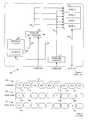
- FIG. 1illustrates a prior art memory storage device with a refresh circuit containing a counter
- FIG. 2illustrates a timing diagram of a memory refresh operation using the memory storage device displayed in FIG. 1;
- FIG. 3illustrates a memory storage device with a refresh circuit with a programmable counter permitting user specification of a wordline to refresh during a refresh operation according to a preferred embodiment of the present invention
- FIG. 4illustrates a timing diagram displaying a memory refresh operation using the memory storage device displayed in FIG. 3;
- FIG. 5illustrates a timing diagram displaying a memory refresh operation using an automatically incrementing programmable counter to refresh a contiguous block of memory according to a preferred embodiment of the present invention
- FIG. 6illustrates the use of refresh command sequences to refresh only portions of memory used to store data according to a preferred embodiment of the present invention
- FIG. 7illustrates an implementation of a single bit slice of a combination programmable counter and latch structure used to implement a refresh circuit with a programmable counter according to a preferred embodiment of the present invention
- FIG. 8illustrates a memory storage device as shown in FIG. 3 that includes the combination programmable counter and latch structure of FIG. 7 .
- FIG. 1a block diagram illustrates a prior art memory storage device 100 with a refresh circuit 140 with a counter 145 according to the technical standard, “PC SDRAM Specification, Revision 1.7, November 1999,” which is incorporated herein by reference.
- the memory storage device 100has preferably three sets of inputs; an address bus, a command bus, and a data input/output (data I/O) bus.
- the address busis used by the user to specify a memory address of a particular memory storage cell or a group of cells in the memory storage device 100 .
- the memory addressmay be thought of as being a combination of a wordline address along with a bitline address of the storage cell(s).
- the command buspermits the user to issue commands to the memory storage device 100 .
- Commandsinclude, but are not limited to: PRE (precharge), ACT (bank/wordline-activate), READ (read data from memory cells), NOP (No operation), etc.
- the data I/O busallows the user to provide or obtain data stored in the memory storage device 100 .
- the memory storage device 100includes: a command interface 110 , a memory storage bank 120 , an address multiplexor 135 , and a refresh circuit 140 .
- the memory storage bank 120may, in turn, be made up of multiple memory storage banks.
- the command interface 110is used to decode the command issued by the user and control the execution of the command.
- the command interface 110is coupled to the memory storage bank 120 by an internal command bus 115 .
- the internal command bus 115provides internal commands that are decoded from user commands by the command interface 110 to the memory storage bank 120 . For example, a PRE (precharge) command would result in an internal command on the internal command bus 115 , causing the deactivation of a wordline in the memory storage bank 120 with an address specified by an internal address bus 155 .
- PREprecharge
- the refresh circuit 140contains a counter 145 .
- the counter 145holds an address of a wordline and a bank number that specifies the wordline that will have its attached memory storage cells refreshed during the next refresh operation.
- the value in the counter 145is incremented (or decremented) after the completion of the refresh operation to provide the address of another wordline for the next refresh operation.
- the address multiplexor 135selects from an address specified by the user or one that is specified by the refresh circuit 140 .
- the command interface 110provides the select line 130 for the address multiplexor 135 and the address selected depends upon the command issued by the user.
- the counter 145is neither writeable nor readable by the user. This means that the user cannot specify an address of a wordline to refresh nor can it detect the wordline that will be refreshed by the refresh operation. This results in several significant disadvantages, including the inability to refresh only the memory storage cells that are actually being used to store data and the necessity of deactivating all wordlines. By having to deactivate all wordlines, the user cannot keep memory banks activated that are not being refreshed by the current refresh operation, resulting in slower memory accesses.
- the usercan perform a user-controlled partial refresh of the memory storage device 100 without using the existing refresh circuit 140 by using a combination of a bank activate (ACT) command and a precharge (PRE) command.
- ACTbank activate
- PREprecharge
- the ACT commandturns on a wordline as specified by the user in a memory bank and row address provided by the user on the address bus.
- the net effect of the ACT commandis that the memory cells connected to the activated wordline are refreshed.
- the succeeding precharge commandthen deactivates the wordline so that other wordlines within the same memory bank can be refreshed.
- FIG. 2a timing diagram illustrates the operation of ACT and PRE commands to perform a user-controlled refresh of a wordline in a memory storage device.
- a first timing trace 210displays the contents of the command bus while a second timing trace 230 displays the bank address portion of the address bus and a third timing trace 240 displays the row address portion of the address bus.
- the refresh operationis displayed in highlight 212 .
- the userspecifies the bank address and the row address of the wordline. This is done by placing the bank and row addresses on the address bus.
- the userplaces the ACT command (block 214 ) on the command bus. For example, FIG. 2 displays a bank address 0 and a row address 011 .
- the usermust wait a specified number of cycles for the refresh operation to complete.
- the usermust wait a time period that is at least equal to four command cycles.
- the userAfter waiting the requisite amount of time, the user must issue a PRE command to deactivate the wordline. To do so, the user places the bank address (bank 0 in the example) and issues the PRE command (block 218 ). The user does not need to specify the row address because the PRE command deactivates all wordlines within a single memory bank.
- Block 222displays the beginning of the next refresh operation while block 220 represents a minimum amount of time between refresh operations. While the time represented by block 220 is shown as a single command cycle, in actuality, it can be greater than one command cycle.
- the average maximum amount of time between refresh operations in a memory device permitting partial refreshis equal to a maximum amount of time that a memory cell can retain it information divided by the number of wordlines in the memory storage cell that require refreshing, while in a memory device that does not permit partial refresh, it is divided by the total number of wordlines.
- FIG. 3a block diagram illustrates a memory storage device 300 with a refresh circuit 340 with a programmable counter 345 according to a preferred embodiment of the present invention.
- the memory storage device 300is similar in operation and layout to the memory storage device 100 displayed in FIG. 1. A notable difference is that the programmable counter 345 used in place of the counter 145 (FIG. 1 ). Additionally, several busses are provided, connecting the programmable counter 345 to an address bus 331 and a command interface 310 .
- a bus 336 between the address bus 331 and the programmable counter 345allows the user to specify the contents of the programmable counter 345 by placing the desired address on the address bus 331 and issuing an appropriate command to load the programmable counter 345 .
- a control signal bus 337 between the command interface 310 and the programmable counter 345allows the command interface 310 , upon the decoding of the appropriate command, to load the value on the address bus 331 into the programmable counter 345 by providing an appropriate load signal on the control signal bus 337 .
- Selection circuitryinside the refresh circuit 340 can enable or disable a connection between the address bus 331 and the programmable counter 345 based upon signals provided by the command interface 310 .
- the selection circuitryenables the bus 336 between the address bus 331 and the programmable counter 345 , resulting in the storing of an address on the address bus 331 in the programmable counter 345 .
- the programmable counter 345maintains the value that it currently stores. The specific command used to load the contents of the programmable counter 345 is discussed below.
- a special commandis used to load the programmable counter 345 .
- the RAP (Row address strobe with Auto Precharge and load) commandloads the value on the address bus 331 into the programmable counter 345 , activates the wordline specified in the address (resulting in the refresh of the memory cells connected to the wordline), and then precharges the wordlines in the memory bank containing the specified wordline.
- the RAP commandis decoded in the command interface into two separate commands.
- a first commandbeing a bank activate command, similar to the RAS (or ACT) command, that activates a wordline in the memory that corresponds to an address specified in the address bus.
- the bank activate commandalso results in the address specified on the address bus being stored in the programmable counter.
- a second command decoded from the RAP commandis a precharge (PRE) command for the particular bank of memory containing the wordline being refreshed.
- PREprecharge
- a signal pinreferred to as an auto precharge control pin in SDRAM circuits, is present in the memory storage device 300 .
- This control pinis used to indicate if an auto precharge operation should be performed at the end of a read or write command as it is known for SDRAM circuits. Additionally, in accordance with the SDRAM interface, the voltage level provided on this control pin distinguishes a precharge for one memory bank from a precharge for all memory banks command.
- this control pinis used to indicate a bank activate command, or RAS, being executed in the memory storage device is a RAS command that is issued by the user or one that is decoded by the command interface 310 resulting from a RAP command issued by the user.
- FIG. 4a timing diagram illustrates the operation of the RAP command to perform a refresh of a wordline in a memory storage device according to a preferred embodiment of the present invention.
- a first timing trace 410displays the contents of the command bus while a second timing trace 420 displays the bank address portion of the address bus and a third timing trace 430 displays the row address portion of the address bus.
- the refresh operationis displayed in highlight 412 .
- the refresh operationbegins when the user writes a bank address and row address of the wordline to be refreshed.
- the writing of the addressesis displayed in blocks 422 and 432 respectively.
- the userissues the RAP command (displayed in block 414 ).
- the userAfter the user issues the RAP command, the user is required to wait a prerequisite amount of time for the refresh operation to complete before the user can access memory storage cells within the memory bank.
- the usersince the user is specifying the wordline that is being refreshed, the user knows which bank of memory the wordline resides in. Because of this knowledge, the user can access other memory cells or other wordlines residing in other memory banks. In fact, the user can perform other refresh operations. In fact, the user can perform as many overlapping refresh operations as there are memory banks in the memory storage device.
- FIG. 4illustrates the beginning of a second refresh operation (displayed in block 416 ) where the user again specifies the address of the wordline that it wishes to refresh.
- a CBR (auto refresh) commandis provided to refresh a wordline that is subsequent to the value stored in the counter in the refresh circuit.
- the CBR commandcan be used to refresh a contiguous sequence of wordlines but only requiring the user to specify the address of only the first wordline in the sequence of wordlines.
- FIG. 5a timing diagram illustrates the operation of the RAP and CBR commands to perform a refresh of a sequence of wordlines in a memory storage device according to a preferred embodiment of the present invention.
- a first timing trace 510displays the contents of the command bus while a second timing trace 520 displays the bank address portion of the address bus and a third timing trace 530 displays the row address portion of the address bus.
- the refresh operationis displayed in highlight 512 .
- the refresh operationbegins when the user writes a bank address and row address of the wordline to be refreshed.
- the writing of the addressesis displayed in blocks 522 and 532 , respectively.
- the userissues the RAP command (displayed in block 514 ).
- the userAfter the user issues the RAP command, the user is required to wait a prerequisite amount of time for the refresh operation to complete before the user can access memory storage cells within the memory bank containing the wordline specified in the address.
- the userissues a CBR command (block 516 ).
- the CBRdoes not require the user to specify the address of any wordline; instead, it takes the contents of the programmable counter in the refresh circuit and increments (or decrements, depending on implementation) its value and performs a refresh operation on the wordline corresponding to the new address.
- the RAP operation(block 514 ) specified a wordline with a bank address 0 and a row address 011 .
- the CBR operation(block 516 ) would then refresh a wordline with a bank address 0 and a row address 100 , assuming the programmable counter is implemented as an autoincrement programmable counter.
- the usercould continue to issue more CBR commands to complete the refreshing of a contiguous block of memory storage cells.
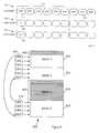
- FIG. 6a block diagram illustrates the use of a RAP command and a sequence of CBR commands to refresh a consecutive sequence of wordlines in a memory storage device according to a preferred embodiment of the present invention.
- FIG. 6illustrates a block of memory 605 comprising four individual memory banks (Bank 0 625 , Bank 1 630 , Bank 2 635 , and Bank 3 640 ).
- FIG. 6also illustrates two sequences of RAP and CBR refresh commands displayed as highlights 610 and 620 .
- the first sequence 610comprising one RAP and three CBR commands and the second sequence 620 comprising one RAP and five CBR commands.
- the first sequence 610starts with a RAP command and the user specifying a wordline address located at the bottom of Bank 0 625 . After the specified wordline is refreshed, the user issues a sequence of three CBR commands to refresh three other wordlines in Bank 0 , which lay in consecutive order to the specified wordline. After the first sequence 610 completes, the user starts the second sequence 620 with another RAP command, specifying a wordline located in Bank 2 635 . After the RAP command completes, the user issues a sequence of five CBR commands to refresh five other wordlines. Note that the wordline refreshed by the third CBR command lies within Bank 3 640 and not Bank 2 635 .
- FIG. 6additionally illustrates several blocks of unused memory, displaying them as shaded blocks 650 and 655 .
- the useris able to refresh the memory storage cells that require refreshing (the storage cells actually used to store data) and the unused memory storage cells are not refreshed. Because the refresh operation consumes a significant amount of power and time, a large amount of power and time can be saved, resulting in more efficient operation and longer battery life and less heat dissipation.
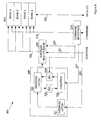
- FIG. 7a block diagram illustrates a single bit slice of a combination programmable counter and latch structure 700 for use in implementing a refresh circuit with programmable counter according to a preferred embodiment of the present invention.
- FIG. 8illustrates the programmable counter and latch structure of FIG. 7 incorporated in the block diagram of FIG. 3 .
- the structure 700is a single bit slice, meaning that a series of these structures can be jointed together to form a multi-bit structure. For example, if a 16 bit programmable counter with latch structure is desired, then a series of 16 of the structures 700 can be combined together to form the 16 bit programmable counter with latch structure.
- the structure 700comprising: a receiver and storage latch circuit 701 , a master-slave flip-flop circuit 702 , a latch and signal driver circuit 703 , a first transmission gate circuit 704 , and a second transmission gate circuit 705 .
- the receiver and storage latch circuit 701is used to store a single bit of an external address provided by the user.
- a receiver 710is used to amplify a single bit of the external address.
- a two cross-coupled inverters 725 and 730are used to store the single bit value placed on the address bus, in a synchronous fashion.
- a transmission gate 720permits the bit value from receiver 710 to propagate to the two cross-coupled inverters 725 and 730 when a first clock input CLKA N is high and when a second clock input CLKA P is low.
- a second transmission gate 735permits the data stored in the cross-coupled inverters 725 and 730 to propagate to the latch and signal driver circuit 703 when clock input CLKA N is low and CLKA P is high.
- the receiver and storage latch circuit 701can be thought of as latching a single bit of the external address with a rising edge on clock CLKA P .
- the master-slave flip-flop circuit 702is constructed of two pairs of cross-coupled inverters, a first pair of cross-coupled inverters comprising inverters 775 and 780 and a second pair of cross-coupled inverters comprising inverters 793 and 795 .
- the output of the second pair of cross-coupled inverters 793 and 795is fed back into the input of the first pair of cross-coupled inverters.
- the additional inverters 785 , 787 , 789 , 791 , and 799the stored bit value toggles between high and low values with each low-high cycle on signal RAC PI
- the output signal RAC PJconnects to the input signal RAC PI of the next bit slice.
- the master-slave flip-flop circuit 702is used to store a single bit of the programmable counter in the refresh circuit.
- a signal CBRRESETis used to allow the clearing of the bit stored in the master-slave flip-flop circuit 702 .
- the latch and signal driver circuit 703stores the data provided by the receiver and storage latch circuit 701 in its own pair of cross-coupled inverters 740 and 745 and an additional inverter 750 inverts and amplifies the stored data to provide sufficient signal strength.
- the data stored in the latch and signal driver circuit 703may be thought of as the internal address that is to be used to access a wordline in the memory storage device.
- inverters 730 , 785 , 791 , 780 , and 795are shown as tristate inverters as they are widely known in the art.
- the input signals, which are switching the inverter from tristate mode into the active mode (and vice-versa),are connected vertically to the inverter on the top and bottom of the inverter.
- the first transmission gate circuit 704comprising a transmission gate 760 and a negative RAP (RAP N ) and positive RAP (RAP P ) signals permit the stored address bit (stored in the latch and signal driver circuit 703 ) to be stored in the master-slave flip-flop circuit 702 .
- RAP Nnegative RAP
- RAP Ppositive RAP
- the output SADD of the latch and signal driver circuit 703is forced onto signal line ADDSET, which is coupled to the master-slave flip-flop circuit 702 . Therefore, the content of the master-slave flip-flop circuit 702 is overwritten by the output SADD of the latch and signal driver circuit 703 .
- the latch and signal driver circuit 703implements the loading of the master-slave flip-flop circuit 702 with an address bit provided by the user.
- the second transmission gate circuit 705comprising a transmission gate 755 and a negative clock (CLKR N ) and a positive clock (CLKR P ) signals permit the stored internal address bit (stored in the master-slave flip-flop circuit 702 ) to overwrite the contents of the latch and signal driver circuit 703 .
- CLKR Nnegative clock
- CLKR Ppositive clock
- the output of the master-slave flip-flop circuit 702overwrites the contents of the latch and signal driver circuit 703 .
- Thisimplements the loading of the internal address stored in the programmable counter onto the internal address bus for use in addressing a wordline, whose address is stored in the programmable counter.
Landscapes
- Engineering & Computer Science (AREA)
- Microelectronics & Electronic Packaging (AREA)
- Computer Hardware Design (AREA)
- Dram (AREA)
Abstract
Description
Claims (33)
Priority Applications (1)
| Application Number | Priority Date | Filing Date | Title |
|---|---|---|---|
| US10/153,042US6665224B1 (en) | 2002-05-22 | 2002-05-22 | Partial refresh for synchronous dynamic random access memory (SDRAM) circuits |
Applications Claiming Priority (1)
| Application Number | Priority Date | Filing Date | Title |
|---|---|---|---|
| US10/153,042US6665224B1 (en) | 2002-05-22 | 2002-05-22 | Partial refresh for synchronous dynamic random access memory (SDRAM) circuits |
Publications (2)
| Publication Number | Publication Date |
|---|---|
| US20030218930A1 US20030218930A1 (en) | 2003-11-27 |
| US6665224B1true US6665224B1 (en) | 2003-12-16 |
Family
ID=29548587
Family Applications (1)
| Application Number | Title | Priority Date | Filing Date |
|---|---|---|---|
| US10/153,042Expired - LifetimeUS6665224B1 (en) | 2002-05-22 | 2002-05-22 | Partial refresh for synchronous dynamic random access memory (SDRAM) circuits |
Country Status (1)
| Country | Link |
|---|---|
| US (1) | US6665224B1 (en) |
Cited By (48)
| Publication number | Priority date | Publication date | Assignee | Title |
|---|---|---|---|---|
| US20040268031A1 (en)* | 2001-09-20 | 2004-12-30 | Lawrence Richard H | System and method for managing data in memory for reducing power consumption |
| US20050132131A1 (en)* | 2003-12-10 | 2005-06-16 | Intel Corporation | Partial bank DRAM precharge |
| US20050237838A1 (en)* | 2004-04-27 | 2005-10-27 | Jong-Tae Kwak | Refresh control circuit and method for multi-bank structure DRAM |
| US20070247953A1 (en)* | 2006-03-21 | 2007-10-25 | Mediatek Inc. | Memory control method and apparatuses |
| US7310281B1 (en)* | 2006-09-01 | 2007-12-18 | Taiwan Semiconductor Manufacturing Co., Ltd. | Semiconductor memories with refreshing cycles |
| US20080056047A1 (en)* | 2004-12-21 | 2008-03-06 | Jain Sandeep K | Method, apparatus, and system for active refresh management |
| US20080158117A1 (en)* | 2006-12-27 | 2008-07-03 | Palm, Inc. | Power saving display |
| US7515453B2 (en) | 2005-06-24 | 2009-04-07 | Metaram, Inc. | Integrated memory core and memory interface circuit |
| US7581127B2 (en) | 2006-07-31 | 2009-08-25 | Metaram, Inc. | Interface circuit system and method for performing power saving operations during a command-related latency |
| US7580312B2 (en) | 2006-07-31 | 2009-08-25 | Metaram, Inc. | Power saving system and method for use with a plurality of memory circuits |
| US7599205B2 (en) | 2005-09-02 | 2009-10-06 | Metaram, Inc. | Methods and apparatus of stacking DRAMs |
| US7609567B2 (en) | 2005-06-24 | 2009-10-27 | Metaram, Inc. | System and method for simulating an aspect of a memory circuit |
| US7730338B2 (en) | 2006-07-31 | 2010-06-01 | Google Inc. | Interface circuit system and method for autonomously performing power management operations in conjunction with a plurality of memory circuits |
| US7761724B2 (en) | 2006-07-31 | 2010-07-20 | Google Inc. | Interface circuit system and method for performing power management operations in conjunction with only a portion of a memory circuit |
| US8019589B2 (en) | 2006-07-31 | 2011-09-13 | Google Inc. | Memory apparatus operable to perform a power-saving operation |
| US8055833B2 (en) | 2006-10-05 | 2011-11-08 | Google Inc. | System and method for increasing capacity, performance, and flexibility of flash storage |
| US8060774B2 (en) | 2005-06-24 | 2011-11-15 | Google Inc. | Memory systems and memory modules |
| US8077535B2 (en) | 2006-07-31 | 2011-12-13 | Google Inc. | Memory refresh apparatus and method |
| US8080874B1 (en) | 2007-09-14 | 2011-12-20 | Google Inc. | Providing additional space between an integrated circuit and a circuit board for positioning a component therebetween |
| US8081474B1 (en) | 2007-12-18 | 2011-12-20 | Google Inc. | Embossed heat spreader |
| US8090897B2 (en) | 2006-07-31 | 2012-01-03 | Google Inc. | System and method for simulating an aspect of a memory circuit |
| US8089795B2 (en) | 2006-02-09 | 2012-01-03 | Google Inc. | Memory module with memory stack and interface with enhanced capabilities |
| US8111566B1 (en) | 2007-11-16 | 2012-02-07 | Google, Inc. | Optimal channel design for memory devices for providing a high-speed memory interface |
| US8130560B1 (en) | 2006-11-13 | 2012-03-06 | Google Inc. | Multi-rank partial width memory modules |
| US20120079183A1 (en)* | 2010-09-24 | 2012-03-29 | Bains Kuljit S | Reduced current requirements for dram self-refresh modes |
| US8154935B2 (en) | 2006-07-31 | 2012-04-10 | Google Inc. | Delaying a signal communicated from a system to at least one of a plurality of memory circuits |
| US8169233B2 (en) | 2009-06-09 | 2012-05-01 | Google Inc. | Programming of DIMM termination resistance values |
| US8209479B2 (en) | 2007-07-18 | 2012-06-26 | Google Inc. | Memory circuit system and method |
| US8244971B2 (en) | 2006-07-31 | 2012-08-14 | Google Inc. | Memory circuit system and method |
| US8280714B2 (en) | 2006-07-31 | 2012-10-02 | Google Inc. | Memory circuit simulation system and method with refresh capabilities |
| US8327104B2 (en) | 2006-07-31 | 2012-12-04 | Google Inc. | Adjusting the timing of signals associated with a memory system |
| US8335894B1 (en) | 2008-07-25 | 2012-12-18 | Google Inc. | Configurable memory system with interface circuit |
| US20130044543A1 (en)* | 2006-11-27 | 2013-02-21 | Mosaid Technologies Incorporated | Non-volatile memory bank and page buffer therefor |
| US8386722B1 (en) | 2008-06-23 | 2013-02-26 | Google Inc. | Stacked DIMM memory interface |
| US8397013B1 (en) | 2006-10-05 | 2013-03-12 | Google Inc. | Hybrid memory module |
| US8438328B2 (en) | 2008-02-21 | 2013-05-07 | Google Inc. | Emulation of abstracted DIMMs using abstracted DRAMs |
| US8566516B2 (en) | 2006-07-31 | 2013-10-22 | Google Inc. | Refresh management of memory modules |
| US8588017B2 (en) | 2010-10-20 | 2013-11-19 | Samsung Electronics Co., Ltd. | Memory circuits, systems, and modules for performing DRAM refresh operations and methods of operating the same |
| US8796830B1 (en) | 2006-09-01 | 2014-08-05 | Google Inc. | Stackable low-profile lead frame package |
| US20140344514A1 (en)* | 2010-12-09 | 2014-11-20 | International Business Machines Corporation | Memory system with a programmable refresh cycle |
| US20150049570A1 (en)* | 2013-08-16 | 2015-02-19 | Sung-Hyun Lee | Memory device, memory system including the same, operating method thereof |
| US8972673B2 (en) | 2006-07-31 | 2015-03-03 | Google Inc. | Power management of memory circuits by virtual memory simulation |
| US9171585B2 (en) | 2005-06-24 | 2015-10-27 | Google Inc. | Configurable memory circuit system and method |
| US9507739B2 (en) | 2005-06-24 | 2016-11-29 | Google Inc. | Configurable memory circuit system and method |
| US9542352B2 (en) | 2006-02-09 | 2017-01-10 | Google Inc. | System and method for reducing command scheduling constraints of memory circuits |
| US9632929B2 (en) | 2006-02-09 | 2017-04-25 | Google Inc. | Translating an address associated with a command communicated between a system and memory circuits |
| US10013371B2 (en) | 2005-06-24 | 2018-07-03 | Google Llc | Configurable memory circuit system and method |
| US10586608B2 (en) | 2015-05-04 | 2020-03-10 | Huawei Technologies Co., Ltd. | DRAM refresh method, apparatus, and system |
Families Citing this family (21)
| Publication number | Priority date | Publication date | Assignee | Title |
|---|---|---|---|---|
| US7236416B2 (en) | 2004-05-21 | 2007-06-26 | Qualcomm Incorporated | Method and system for controlling refresh in volatile memories |
| TWI260019B (en)* | 2004-05-21 | 2006-08-11 | Fujitsu Ltd | Semiconductor memory device and memory system |
| US7088633B2 (en)* | 2004-05-27 | 2006-08-08 | Qualcomm Incorporated | Method and system for providing seamless self-refresh for directed bank refresh in volatile memories |
| US7953921B2 (en)* | 2004-12-28 | 2011-05-31 | Qualcomm Incorporated | Directed auto-refresh synchronization |
| US8521970B2 (en) | 2006-04-19 | 2013-08-27 | Lexmark International, Inc. | Addressing, command protocol, and electrical interface for non-volatile memories utilized in recording usage counts |
| US9245591B2 (en) | 2005-06-16 | 2016-01-26 | Lexmark International, Inc. | Addressing, command protocol, and electrical interface for non-volatile memories utilized in recording usage counts |
| US7426613B2 (en)* | 2005-06-16 | 2008-09-16 | Lexmark International, Inc. | Addressing, command protocol, and electrical interface for non-volatile memories utilized in recording usage counts |
| US7313047B2 (en)* | 2006-02-23 | 2007-12-25 | Hynix Semiconductor Inc. | Dynamic semiconductor memory with improved refresh mechanism |
| US8024513B2 (en)* | 2007-12-04 | 2011-09-20 | International Business Machines Corporation | Method and system for implementing dynamic refresh protocols for DRAM based cache |
| US7962695B2 (en)* | 2007-12-04 | 2011-06-14 | International Business Machines Corporation | Method and system for integrating SRAM and DRAM architecture in set associative cache |
| US8108609B2 (en)* | 2007-12-04 | 2012-01-31 | International Business Machines Corporation | Structure for implementing dynamic refresh protocols for DRAM based cache |
| US20090144507A1 (en)* | 2007-12-04 | 2009-06-04 | International Business Machines Corporation | APPARATUS AND METHOD FOR IMPLEMENTING REFRESHLESS SINGLE TRANSISTOR CELL eDRAM FOR HIGH PERFORMANCE MEMORY APPLICATIONS |
| US20090144504A1 (en)* | 2007-12-04 | 2009-06-04 | International Business Machines Corporation | STRUCTURE FOR IMPLEMENTING REFRESHLESS SINGLE TRANSISTOR CELL eDRAM FOR HIGH PERFORMANCE MEMORY APPLICATIONS |
| US7882302B2 (en)* | 2007-12-04 | 2011-02-01 | International Business Machines Corporation | Method and system for implementing prioritized refresh of DRAM based cache |
| JP5599977B2 (en)* | 2009-01-22 | 2014-10-01 | ピーエスフォー ルクスコ エスエイアールエル | Semiconductor memory device |
| KR101993794B1 (en) | 2012-06-14 | 2019-06-27 | 삼성전자주식회사 | Memory device, operation method thereof and memory system having the same |
| WO2016078731A1 (en) | 2014-11-21 | 2016-05-26 | Telefonaktiebolaget L M Ericsson (Publ) | Signal processing apparatus and method |
| US10141042B1 (en)* | 2017-05-23 | 2018-11-27 | Micron Technology, Inc. | Method and apparatus for precharge and refresh control |
| CN112448979B (en)* | 2019-08-30 | 2022-09-13 | 贵州白山云科技股份有限公司 | Cache information updating method, device and medium |
| KR102833439B1 (en)* | 2019-11-01 | 2025-07-10 | 삼성전자주식회사 | Memory device including processing element, and memory system including the memory device |
| EP4033365A1 (en) | 2021-01-25 | 2022-07-27 | Nordic Semiconductor ASA | Memory retention for radio device |
Citations (6)
| Publication number | Priority date | Publication date | Assignee | Title |
|---|---|---|---|---|
| US5331601A (en) | 1993-02-04 | 1994-07-19 | United Memories, Inc. | DRAM variable row select |
| US5600802A (en)* | 1994-03-14 | 1997-02-04 | Apple Computer, Inc. | Methods and apparatus for translating incompatible bus transactions |
| US5875143A (en) | 1996-07-15 | 1999-02-23 | Motorola, Inc. | Dynamic memory device with refresh circuit and refresh method |
| US6064617A (en)* | 1998-04-28 | 2000-05-16 | Micron Technology, Inc. | Method and apparatus for strobing antifuse circuits in a memory device |
| US6310814B1 (en)* | 1998-03-10 | 2001-10-30 | Rambus, Inc. | Rambus DRAM (RDRAM) apparatus and method for performing refresh operations |
| US6496440B2 (en)* | 1999-03-01 | 2002-12-17 | Micron Technology, Inc. | Method and system for accessing rows in multiple memory banks within an integrated circuit |
- 2002
- 2002-05-22USUS10/153,042patent/US6665224B1/ennot_activeExpired - Lifetime
Patent Citations (6)
| Publication number | Priority date | Publication date | Assignee | Title |
|---|---|---|---|---|
| US5331601A (en) | 1993-02-04 | 1994-07-19 | United Memories, Inc. | DRAM variable row select |
| US5600802A (en)* | 1994-03-14 | 1997-02-04 | Apple Computer, Inc. | Methods and apparatus for translating incompatible bus transactions |
| US5875143A (en) | 1996-07-15 | 1999-02-23 | Motorola, Inc. | Dynamic memory device with refresh circuit and refresh method |
| US6310814B1 (en)* | 1998-03-10 | 2001-10-30 | Rambus, Inc. | Rambus DRAM (RDRAM) apparatus and method for performing refresh operations |
| US6064617A (en)* | 1998-04-28 | 2000-05-16 | Micron Technology, Inc. | Method and apparatus for strobing antifuse circuits in a memory device |
| US6496440B2 (en)* | 1999-03-01 | 2002-12-17 | Micron Technology, Inc. | Method and system for accessing rows in multiple memory banks within an integrated circuit |
Cited By (90)
| Publication number | Priority date | Publication date | Assignee | Title |
|---|---|---|---|---|
| US20040268031A1 (en)* | 2001-09-20 | 2004-12-30 | Lawrence Richard H | System and method for managing data in memory for reducing power consumption |
| US7380048B2 (en)* | 2001-09-20 | 2008-05-27 | Intel Corporation | System and method for managing data in memory for reducing power consumption |
| US7392339B2 (en)* | 2003-12-10 | 2008-06-24 | Intel Corporation | Partial bank DRAM precharge |
| US20050132131A1 (en)* | 2003-12-10 | 2005-06-16 | Intel Corporation | Partial bank DRAM precharge |
| US20050237838A1 (en)* | 2004-04-27 | 2005-10-27 | Jong-Tae Kwak | Refresh control circuit and method for multi-bank structure DRAM |
| US7145827B2 (en) | 2004-04-27 | 2006-12-05 | Hynix Semiconductor, Inc. | Refresh control circuit and method for multi-bank structure DRAM |
| US20070070768A1 (en)* | 2004-04-27 | 2007-03-29 | Jong-Tae Kwak | Refresh control circuit and method for multi-bank structure DRAM |
| US7260010B2 (en) | 2004-04-27 | 2007-08-21 | Hynix Semiconductor Inc. | Refresh control circuit and method for multi-bank structure DRAM |
| US8289797B2 (en)* | 2004-12-21 | 2012-10-16 | Intel Corporation | Method, apparatus, and system for active refresh management |
| US20080056047A1 (en)* | 2004-12-21 | 2008-03-06 | Jain Sandeep K | Method, apparatus, and system for active refresh management |
| US8615679B2 (en) | 2005-06-24 | 2013-12-24 | Google Inc. | Memory modules with reliability and serviceability functions |
| US9507739B2 (en) | 2005-06-24 | 2016-11-29 | Google Inc. | Configurable memory circuit system and method |
| US8359187B2 (en) | 2005-06-24 | 2013-01-22 | Google Inc. | Simulating a different number of memory circuit devices |
| US7515453B2 (en) | 2005-06-24 | 2009-04-07 | Metaram, Inc. | Integrated memory core and memory interface circuit |
| US8386833B2 (en) | 2005-06-24 | 2013-02-26 | Google Inc. | Memory systems and memory modules |
| US8060774B2 (en) | 2005-06-24 | 2011-11-15 | Google Inc. | Memory systems and memory modules |
| US10013371B2 (en) | 2005-06-24 | 2018-07-03 | Google Llc | Configurable memory circuit system and method |
| US9171585B2 (en) | 2005-06-24 | 2015-10-27 | Google Inc. | Configurable memory circuit system and method |
| US7609567B2 (en) | 2005-06-24 | 2009-10-27 | Metaram, Inc. | System and method for simulating an aspect of a memory circuit |
| US8582339B2 (en) | 2005-09-02 | 2013-11-12 | Google Inc. | System including memory stacks |
| US7599205B2 (en) | 2005-09-02 | 2009-10-06 | Metaram, Inc. | Methods and apparatus of stacking DRAMs |
| US8811065B2 (en) | 2005-09-02 | 2014-08-19 | Google Inc. | Performing error detection on DRAMs |
| US8619452B2 (en) | 2005-09-02 | 2013-12-31 | Google Inc. | Methods and apparatus of stacking DRAMs |
| US8797779B2 (en) | 2006-02-09 | 2014-08-05 | Google Inc. | Memory module with memory stack and interface with enhanced capabilites |
| US9542352B2 (en) | 2006-02-09 | 2017-01-10 | Google Inc. | System and method for reducing command scheduling constraints of memory circuits |
| US9542353B2 (en) | 2006-02-09 | 2017-01-10 | Google Inc. | System and method for reducing command scheduling constraints of memory circuits |
| US9727458B2 (en) | 2006-02-09 | 2017-08-08 | Google Inc. | Translating an address associated with a command communicated between a system and memory circuits |
| US8566556B2 (en) | 2006-02-09 | 2013-10-22 | Google Inc. | Memory module with memory stack and interface with enhanced capabilities |
| US9632929B2 (en) | 2006-02-09 | 2017-04-25 | Google Inc. | Translating an address associated with a command communicated between a system and memory circuits |
| US8089795B2 (en) | 2006-02-09 | 2012-01-03 | Google Inc. | Memory module with memory stack and interface with enhanced capabilities |
| US7408832B2 (en)* | 2006-03-21 | 2008-08-05 | Mediatek Inc. | Memory control method and apparatuses |
| US20070247953A1 (en)* | 2006-03-21 | 2007-10-25 | Mediatek Inc. | Memory control method and apparatuses |
| US8340953B2 (en) | 2006-07-31 | 2012-12-25 | Google, Inc. | Memory circuit simulation with power saving capabilities |
| US8595419B2 (en) | 2006-07-31 | 2013-11-26 | Google Inc. | Memory apparatus operable to perform a power-saving operation |
| US8671244B2 (en) | 2006-07-31 | 2014-03-11 | Google Inc. | Simulating a memory standard |
| US8154935B2 (en) | 2006-07-31 | 2012-04-10 | Google Inc. | Delaying a signal communicated from a system to at least one of a plurality of memory circuits |
| US7581127B2 (en) | 2006-07-31 | 2009-08-25 | Metaram, Inc. | Interface circuit system and method for performing power saving operations during a command-related latency |
| US7580312B2 (en) | 2006-07-31 | 2009-08-25 | Metaram, Inc. | Power saving system and method for use with a plurality of memory circuits |
| US8244971B2 (en) | 2006-07-31 | 2012-08-14 | Google Inc. | Memory circuit system and method |
| US8280714B2 (en) | 2006-07-31 | 2012-10-02 | Google Inc. | Memory circuit simulation system and method with refresh capabilities |
| US7590796B2 (en) | 2006-07-31 | 2009-09-15 | Metaram, Inc. | System and method for power management in memory systems |
| US8327104B2 (en) | 2006-07-31 | 2012-12-04 | Google Inc. | Adjusting the timing of signals associated with a memory system |
| US7730338B2 (en) | 2006-07-31 | 2010-06-01 | Google Inc. | Interface circuit system and method for autonomously performing power management operations in conjunction with a plurality of memory circuits |
| US8112266B2 (en) | 2006-07-31 | 2012-02-07 | Google Inc. | Apparatus for simulating an aspect of a memory circuit |
| US8090897B2 (en) | 2006-07-31 | 2012-01-03 | Google Inc. | System and method for simulating an aspect of a memory circuit |
| US8631220B2 (en) | 2006-07-31 | 2014-01-14 | Google Inc. | Adjusting the timing of signals associated with a memory system |
| US7761724B2 (en) | 2006-07-31 | 2010-07-20 | Google Inc. | Interface circuit system and method for performing power management operations in conjunction with only a portion of a memory circuit |
| US9047976B2 (en) | 2006-07-31 | 2015-06-02 | Google Inc. | Combined signal delay and power saving for use with a plurality of memory circuits |
| US8041881B2 (en) | 2006-07-31 | 2011-10-18 | Google Inc. | Memory device with emulated characteristics |
| US8601204B2 (en) | 2006-07-31 | 2013-12-03 | Google Inc. | Simulating a refresh operation latency |
| US8972673B2 (en) | 2006-07-31 | 2015-03-03 | Google Inc. | Power management of memory circuits by virtual memory simulation |
| US8745321B2 (en) | 2006-07-31 | 2014-06-03 | Google Inc. | Simulating a memory standard |
| US8019589B2 (en) | 2006-07-31 | 2011-09-13 | Google Inc. | Memory apparatus operable to perform a power-saving operation |
| US8868829B2 (en) | 2006-07-31 | 2014-10-21 | Google Inc. | Memory circuit system and method |
| US8566516B2 (en) | 2006-07-31 | 2013-10-22 | Google Inc. | Refresh management of memory modules |
| US8077535B2 (en) | 2006-07-31 | 2011-12-13 | Google Inc. | Memory refresh apparatus and method |
| US8796830B1 (en) | 2006-09-01 | 2014-08-05 | Google Inc. | Stackable low-profile lead frame package |
| US7310281B1 (en)* | 2006-09-01 | 2007-12-18 | Taiwan Semiconductor Manufacturing Co., Ltd. | Semiconductor memories with refreshing cycles |
| US8397013B1 (en) | 2006-10-05 | 2013-03-12 | Google Inc. | Hybrid memory module |
| US8055833B2 (en) | 2006-10-05 | 2011-11-08 | Google Inc. | System and method for increasing capacity, performance, and flexibility of flash storage |
| US8977806B1 (en) | 2006-10-05 | 2015-03-10 | Google Inc. | Hybrid memory module |
| US8370566B2 (en) | 2006-10-05 | 2013-02-05 | Google Inc. | System and method for increasing capacity, performance, and flexibility of flash storage |
| US8751732B2 (en) | 2006-10-05 | 2014-06-10 | Google Inc. | System and method for increasing capacity, performance, and flexibility of flash storage |
| US8446781B1 (en) | 2006-11-13 | 2013-05-21 | Google Inc. | Multi-rank partial width memory modules |
| US8130560B1 (en) | 2006-11-13 | 2012-03-06 | Google Inc. | Multi-rank partial width memory modules |
| US8760936B1 (en) | 2006-11-13 | 2014-06-24 | Google Inc. | Multi-rank partial width memory modules |
| US8879351B2 (en)* | 2006-11-27 | 2014-11-04 | Conversant Intellectual Property Management Inc. | Non-volatile memory bank and page buffer therefor |
| US20130044543A1 (en)* | 2006-11-27 | 2013-02-21 | Mosaid Technologies Incorporated | Non-volatile memory bank and page buffer therefor |
| US20080158117A1 (en)* | 2006-12-27 | 2008-07-03 | Palm, Inc. | Power saving display |
| US7995050B2 (en) | 2006-12-27 | 2011-08-09 | Hewlett-Packard Development Company, L.P. | Power saving display |
| US8209479B2 (en) | 2007-07-18 | 2012-06-26 | Google Inc. | Memory circuit system and method |
| US8080874B1 (en) | 2007-09-14 | 2011-12-20 | Google Inc. | Providing additional space between an integrated circuit and a circuit board for positioning a component therebetween |
| US8675429B1 (en) | 2007-11-16 | 2014-03-18 | Google Inc. | Optimal channel design for memory devices for providing a high-speed memory interface |
| US8111566B1 (en) | 2007-11-16 | 2012-02-07 | Google, Inc. | Optimal channel design for memory devices for providing a high-speed memory interface |
| US8705240B1 (en) | 2007-12-18 | 2014-04-22 | Google Inc. | Embossed heat spreader |
| US8730670B1 (en) | 2007-12-18 | 2014-05-20 | Google Inc. | Embossed heat spreader |
| US8081474B1 (en) | 2007-12-18 | 2011-12-20 | Google Inc. | Embossed heat spreader |
| US8631193B2 (en) | 2008-02-21 | 2014-01-14 | Google Inc. | Emulation of abstracted DIMMS using abstracted DRAMS |
| US8438328B2 (en) | 2008-02-21 | 2013-05-07 | Google Inc. | Emulation of abstracted DIMMs using abstracted DRAMs |
| US8386722B1 (en) | 2008-06-23 | 2013-02-26 | Google Inc. | Stacked DIMM memory interface |
| US8762675B2 (en) | 2008-06-23 | 2014-06-24 | Google Inc. | Memory system for synchronous data transmission |
| US8819356B2 (en) | 2008-07-25 | 2014-08-26 | Google Inc. | Configurable multirank memory system with interface circuit |
| US8335894B1 (en) | 2008-07-25 | 2012-12-18 | Google Inc. | Configurable memory system with interface circuit |
| US8169233B2 (en) | 2009-06-09 | 2012-05-01 | Google Inc. | Programming of DIMM termination resistance values |
| US20120079183A1 (en)* | 2010-09-24 | 2012-03-29 | Bains Kuljit S | Reduced current requirements for dram self-refresh modes |
| US8411523B2 (en)* | 2010-09-24 | 2013-04-02 | Intel Corporation | Reduced current requirements for DRAM self-refresh modes via staggered refresh operations of subsets of memory banks or rows |
| US8588017B2 (en) | 2010-10-20 | 2013-11-19 | Samsung Electronics Co., Ltd. | Memory circuits, systems, and modules for performing DRAM refresh operations and methods of operating the same |
| US20140344514A1 (en)* | 2010-12-09 | 2014-11-20 | International Business Machines Corporation | Memory system with a programmable refresh cycle |
| US20150049570A1 (en)* | 2013-08-16 | 2015-02-19 | Sung-Hyun Lee | Memory device, memory system including the same, operating method thereof |
| US10586608B2 (en) | 2015-05-04 | 2020-03-10 | Huawei Technologies Co., Ltd. | DRAM refresh method, apparatus, and system |
Also Published As
| Publication number | Publication date |
|---|---|
| US20030218930A1 (en) | 2003-11-27 |
Similar Documents
| Publication | Publication Date | Title |
|---|---|---|
| US6665224B1 (en) | Partial refresh for synchronous dynamic random access memory (SDRAM) circuits | |
| US10127969B2 (en) | Memory device command receiving and decoding methods | |
| US6741515B2 (en) | DRAM with total self refresh and control circuit | |
| US6618314B1 (en) | Method and architecture for reducing the power consumption for memory devices in refresh operations | |
| US6252807B1 (en) | Memory device with reduced power consumption when byte-unit accessed | |
| KR100963702B1 (en) | System and method for decoding commands based on command signals and operational status | |
| US6751159B2 (en) | Memory device operable in either a high-power, full-page size mode or a low-power, reduced-page size mode | |
| US8369168B2 (en) | Devices and system providing reduced quantity of interconnections | |
| US7405992B2 (en) | Method and apparatus for communicating command and address signals | |
| US20030043658A1 (en) | Memory device and method having data path with multiple prefetch I/O configurations | |
| KR20030038450A (en) | Memory device and internal control method therefor | |
| US5848431A (en) | Synchronous SRAMs having multiple chip select inputs and a standby chip enable input | |
| CN100495568C (en) | Method for accessing data and device and system using the method | |
| JP3531602B2 (en) | Activation of word lines in semiconductor memory devices | |
| US20020136079A1 (en) | Semiconductor memory device and information processing system | |
| US6192002B1 (en) | Memory device with command buffer | |
| KR100305648B1 (en) | High-speed dram | |
| JP2004185686A (en) | Semiconductor storage device | |
| CN118072787A (en) | ODT control circuit and memory | |
| CN111240582B (en) | Data reading and writing method, reading and writing device and dynamic random access memory | |
| JP4012393B2 (en) | Storage device, internal control method and system for storage device, and control method for storage means in system | |
| US5946269A (en) | Synchronous RAM controlling device and method | |
| US6822920B2 (en) | SRAM-compatible memory device employing DRAM cells | |
| JPH0877769A (en) | Synchronous semiconductor memory device | |
| CN111241007A (en) | Data reading and writing method and device and dynamic random access memory |
Legal Events
| Date | Code | Title | Description |
|---|---|---|---|
| AS | Assignment | Owner name:INFINEON TECHNOLOGIES NORTH AMERICA CORP., CALIFOR Free format text:ASSIGNMENT OF ASSIGNORS INTEREST;ASSIGNORS:LEHMANN, GUNTHER;MENKE, MANFRED;REEL/FRAME:013851/0301;SIGNING DATES FROM 20020514 TO 20020521 | |
| AS | Assignment | Owner name:INFINEON TECHNOLOGIES AG, GERMANY Free format text:ASSIGNMENT OF ASSIGNORS INTEREST;ASSIGNOR:INFINEON TECHNOLOGIES NORTH AMERICA CORP.;REEL/FRAME:014697/0674 Effective date:20031009 | |
| STCF | Information on status: patent grant | Free format text:PATENTED CASE | |
| FEPP | Fee payment procedure | Free format text:PAYOR NUMBER ASSIGNED (ORIGINAL EVENT CODE: ASPN); ENTITY STATUS OF PATENT OWNER: LARGE ENTITY | |
| FEPP | Fee payment procedure | Free format text:PAYER NUMBER DE-ASSIGNED (ORIGINAL EVENT CODE: RMPN); ENTITY STATUS OF PATENT OWNER: LARGE ENTITY Free format text:PAYOR NUMBER ASSIGNED (ORIGINAL EVENT CODE: ASPN); ENTITY STATUS OF PATENT OWNER: LARGE ENTITY | |
| FPAY | Fee payment | Year of fee payment:4 | |
| FPAY | Fee payment | Year of fee payment:8 | |
| FPAY | Fee payment | Year of fee payment:12 | |
| AS | Assignment | Owner name:POLARIS INNOVATIONS LIMITED, IRELAND Free format text:ASSIGNMENT OF ASSIGNORS INTEREST;ASSIGNOR:INFINEON TECHNOLOGIES AG;REEL/FRAME:036827/0885 Effective date:20150708 | |
| AS | Assignment | Owner name:POLARIS INNOVATIONS LIMITED, IRELAND Free format text:CORRECTIVE ASSIGNMENT TO CORRECT THE PATENT 7105729 PREVIOUSLY RECORDED AT REEL: 036827 FRAME: 0885. ASSIGNOR(S) HEREBY CONFIRMS THE ASSIGNMENT;ASSIGNOR:INFINEON TECHNOLOGIES AG;REEL/FRAME:043336/0694 Effective date:20150708 |