US6664853B1 - Wide-bandwidth differential signal amplifier - Google Patents
Wide-bandwidth differential signal amplifierDownload PDFInfo
- Publication number
- US6664853B1 US6664853B1US10/061,735US6173502AUS6664853B1US 6664853 B1US6664853 B1US 6664853B1US 6173502 AUS6173502 AUS 6173502AUS 6664853 B1US6664853 B1US 6664853B1
- Authority
- US
- United States
- Prior art keywords
- amplifier
- fet
- cmosfet
- source
- output
- Prior art date
- Legal status (The legal status is an assumption and is not a legal conclusion. Google has not performed a legal analysis and makes no representation as to the accuracy of the status listed.)
- Expired - Lifetime
Links
- 239000003990capacitorSubstances0.000claimsdescription22
- 238000000034methodMethods0.000claimsdescription15
- 230000005669field effectEffects0.000claimsdescription13
- 239000004065semiconductorSubstances0.000claimsdescription10
- 230000000295complement effectEffects0.000claimsdescription9
- 229910044991metal oxideInorganic materials0.000claimsdescription8
- 150000004706metal oxidesChemical class0.000claimsdescription8
- 238000010586diagramMethods0.000description6
- 230000007423decreaseEffects0.000description2
- RGNPBRKPHBKNKX-UHFFFAOYSA-NhexaflumuronChemical compoundC1=C(Cl)C(OC(F)(F)C(F)F)=C(Cl)C=C1NC(=O)NC(=O)C1=C(F)C=CC=C1FRGNPBRKPHBKNKX-UHFFFAOYSA-N0.000description2
- 238000004519manufacturing processMethods0.000description2
- 238000012986modificationMethods0.000description2
- 230000004048modificationEffects0.000description2
- JBRZTFJDHDCESZ-UHFFFAOYSA-NAsGaChemical compound[As]#[Ga]JBRZTFJDHDCESZ-UHFFFAOYSA-N0.000description1
- XUIMIQQOPSSXEZ-UHFFFAOYSA-NSiliconChemical compound[Si]XUIMIQQOPSSXEZ-UHFFFAOYSA-N0.000description1
- 230000003321amplificationEffects0.000description1
- 230000003139buffering effectEffects0.000description1
- 238000007796conventional methodMethods0.000description1
- 238000005530etchingMethods0.000description1
- 229910052732germaniumInorganic materials0.000description1
- GNPVGFCGXDBREM-UHFFFAOYSA-Ngermanium atomChemical compound[Ge]GNPVGFCGXDBREM-UHFFFAOYSA-N0.000description1
- 239000000463materialSubstances0.000description1
- 238000003199nucleic acid amplification methodMethods0.000description1
- 230000008054signal transmissionEffects0.000description1
- 229910052710siliconInorganic materials0.000description1
- 239000010703siliconSubstances0.000description1
Images


Classifications
- H—ELECTRICITY
- H03—ELECTRONIC CIRCUITRY
- H03F—AMPLIFIERS
- H03F3/00—Amplifiers with only discharge tubes or only semiconductor devices as amplifying elements
- H03F3/45—Differential amplifiers
- H03F3/45071—Differential amplifiers with semiconductor devices only
- H03F3/45076—Differential amplifiers with semiconductor devices only characterised by the way of implementation of the active amplifying circuit in the differential amplifier
- H03F3/45179—Differential amplifiers with semiconductor devices only characterised by the way of implementation of the active amplifying circuit in the differential amplifier using MOSFET transistors as the active amplifying circuit
- H03F3/45197—Pl types
- H—ELECTRICITY
- H03—ELECTRONIC CIRCUITRY
- H03F—AMPLIFIERS
- H03F2203/00—Indexing scheme relating to amplifiers with only discharge tubes or only semiconductor devices as amplifying elements covered by H03F3/00
- H03F2203/45—Indexing scheme relating to differential amplifiers
- H03F2203/45458—Indexing scheme relating to differential amplifiers the CSC comprising one or more capacitors
- H—ELECTRICITY
- H03—ELECTRONIC CIRCUITRY
- H03F—AMPLIFIERS
- H03F2203/00—Indexing scheme relating to amplifiers with only discharge tubes or only semiconductor devices as amplifying elements covered by H03F3/00
- H03F2203/45—Indexing scheme relating to differential amplifiers
- H03F2203/45496—Indexing scheme relating to differential amplifiers the CSC comprising one or more extra resistors
- H—ELECTRICITY
- H03—ELECTRONIC CIRCUITRY
- H03F—AMPLIFIERS
- H03F2203/00—Indexing scheme relating to amplifiers with only discharge tubes or only semiconductor devices as amplifying elements covered by H03F3/00
- H03F2203/45—Indexing scheme relating to differential amplifiers
- H03F2203/45631—Indexing scheme relating to differential amplifiers the LC comprising one or more capacitors, e.g. coupling capacitors
- H—ELECTRICITY
- H03—ELECTRONIC CIRCUITRY
- H03F—AMPLIFIERS
- H03F2203/00—Indexing scheme relating to amplifiers with only discharge tubes or only semiconductor devices as amplifying elements covered by H03F3/00
- H03F2203/45—Indexing scheme relating to differential amplifiers
- H03F2203/45702—Indexing scheme relating to differential amplifiers the LC comprising two resistors
Definitions
- the inventionrelates in general to electronic circuits and more specifically to differential signal amplifiers.
- Differential signal amplifiersamplify a differential signal to form an amplified differential output signal and can be used for a variety of purposes and within different types of circuits.
- the differential signal amplifierproduces a differential output signal from a differential input signal that includes two signals where each of the two signals is complementary to the other.
- Typical uses of differential signal amplifiersinclude using an amplifier with a gain greater than 1 to increase the amplitude of the input signal.
- Several differential signal amplifiersmay be connected to form an amplifier with a higher gain. Other uses include using the amplifier as a buffer between circuits.
- Applications for differential signal amplifiersinclude uses within current mode logic (CML) circuits.
- Another exampleincludes high frequency postamplifiers for use in high speed circuits such as SONET transceivers. Complementary Metal Oxide Semiconductor (CMOS) techniques are often used to manufacture the amplifiers.
- CMLcurrent mode logic
- CMOSComplementary Metal Oxide Semiconductor
- a wide-bandwidth amplifierincludes a pair of transistors having output ports connected to two current sources and an impedance element connected between the output ports.
- the impedance elementcreates a zero resulting a wide-bandwidth frequency response of the amplifier.
- FIG. 1is a block diagram of a wide-bandwidth amplifier in accordance with an exemplary embodiment of the invention.
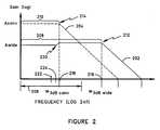
- FIG. 2is graphical representation of a frequency response of the wide-band amplifier in accordance with the exemplary embodiment of the invention.
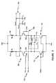
- FIG. 3is a schematic diagram of the wide-band amplifier in accordance with the exemplary embodiment where the transistors are implemented using Complementary Metal Oxide Semiconductor (CMOS) field effect transistors (FETs).
- CMOSComplementary Metal Oxide Semiconductor
- FETsfield effect transistors
- FIG. 4is a flow chart of method of forming the differential output signal in accordance with the exemplary embodiment of the invention.
- FIG. 5is a block diagram of a top view representation of an Integrated Circuit (IC) in accordance with the exemplary embodiment of the invention.
- ICIntegrated Circuit
- FIG. 1is a block diagram of a wide-bandwidth amplifier 100 in accordance with exemplary embodiment of the invention.
- the wide-bandwidth amplifier 100may be implemented using discrete components, in an integrated circuit (IC) or in any combination of integrated circuits and discrete components formed in accordance with any single manufacturing technique or combination of techniques.
- the wide-bandwidth amplifier 100is implemented with field effect transistors (FETs) within an integrated circuit in accordance with the teachings herein and known techniques.
- FETsfield effect transistors
- the wide-bandwidth amplifier 100can be used for a variety of circuits. Several amplifiers 100 may be connected to form an amplifier with a higher overall gain.
- An example of a suitable use for the amplifier 100includes implementing the amplifier 100 in accordance with CMOS techniques for use within a postamplifier within a SONET transceiver for high speed transmission of signals.
- the wide-bandwidth amplifier 100amplifies a differential input signal received across an amplifier input 102 to produce a differential output signal at an amplifier output 104 .
- the amplifier 100has a gain that is greater than 1, the amplifier 100 can be used as an output buffer or for other purposes where the amplitude of the output signal does not need to be greater than the input signal and the gain of the amplifier is less than 1.
- the amplifier 100includes at least two transistors 106 , 108 , two current sources 110 , 112 and an impedance element 114 .
- the inputs 116 , 118 of the transistorsare connected to a supply voltage (VDD) through load resistors 120 , 122 .
- Each current source 110 , 112is connected between an output port 128 , 130 of a transistor 106 , 108 and a voltage reference (VSS) such as ground.
- the impedance element 114is connected between the two output ports 128 , 130 of the transistors 106 , 108 .
- the transistors 106 , 108are Complementary Metal Oxide Semiconductor (CMOS) field effect transistors (FETs), the invention is not limited to any particular type of transistor or semiconductor technology.
- CMOSComplementary Metal Oxide Semiconductor
- the input ports ( 116 , 118 ), control ports ( 124 , 126 ) and the output ports 128 , 130respectively correspond to the drain, gate and source of a field effect transistor (FET) and to the collector, base and emitter of a bipolar junction transistor (BJT).
- CMOSComplementary Metal Oxide Semiconductor
- the impedance elementcan be a resistor connected in parallel to a capacitor.
- the impedance element 114creates a zero in the frequency response resulting in a higher bandwidth frequency response as compared to a conventional amplifier using a single current source connected to both output ports 128 , 130 of the transistors 106 , 108 .
- FIG. 2is graphical representation of a frequency response 202 of the wide-bandwidth amplifier 100 compared to a frequency response 204 of a conventional amplifier where both output ports 124 , 126 of the transistors 106 , 108 are connected to a single current source ( 110 , 112 ).
- the gain, A wideof the wide-bandwidth amplifier 100 is less than the gain, A conv , of a conventional amplifier without an impedance element 114 .
- the bandwidth 208however, of the wide-bandwidth amplifier 100 is greater than the bandwidth 210 of the conventional amplifier.
- the bandwidths 208 , 210are defined as 3 dB bandwidths.
- the 3 dB points ⁇ 3dBwide 212 and ⁇ 3dBconv 214indicate the frequencies 216 , 218 where the gain is 3 dB below the low frequency gain (A conv , A wide ).
- the impedance element 114provides a zero resulting in a higher bandwidth frequency response 202 .
- a poleis formed in the frequency response.
- the frequency location 224 of the poledepends on the impedance element, the impedance of the load at the output 104 and the characteristics of the transistors 106 , 108 . In certain situations, the zero-pole combination results in a disturbance 220 in the frequency response 202 of the wide-bandwidth amplifier 100 .
- the impedance element 114is selected to minimize the disturbance 220 and, therefore, to maintain the frequency response 202 as flat as possible.
- the frequency locations 224 , 222 of the pole and zerocan be arranged by adjusting several parameters and, in many situations, are selected to closely space the zero and pole frequency locations 222 , 224 and maintain a relatively flat frequency response.
- FIG. 3is a schematic diagram of the wide-band amplifier 100 in accordance with the exemplary embodiment where the transistors 106 , 108 are Complementary Metal Oxide Semiconductor (CMOS) field effect transistors (FETs).
- the current sourcesare CMOS transistors that are biased at a bias voltage (Vbias).
- the impedance element 114is a resistor 302 , having a value of Rc, connected in parallel to a capacitor 304 having a value of Cc.
- the resistor 302 and capacitor 304create a zero resulting in a frequency response 202 having a wider bandwidth than conventional amplifiers without an increase in power dissipation.
- the capacitor 304has a high impedance allowing the resistor 302 to be the dominant impedance between the two output two sources 128 , 130 of the transistors 106 , 108 . At higher frequencies, the capacitor 304 begins to appear as a short between the sources 128 , 130 reducing the overall impedance of the impedance element 114 .
- the values (Rc, Cc) of the resistor 302 and capacitor 304are selected such that the frequency response is maintained as close as possible to a constant gain within the desired band of operation.
- Ccis chosen such that the impedance element 114 begins to appear as short at the same frequency that the capacitance (CL) of loads at the amplifier output 104 begins to short out the resistors 120 , 122 .
- the appropriate values of the resistor 302 and the capacitor 304 for a particular wide-bandwidth amplifier 100can be selected by using the equations below in accordance with known techniques and the teachings herein.
- the characteristics of the wide-bandwidth amplifiercan be approximated by the following equations, where g m is the transconductance of the transistors, r o is the internal output resistance, S zero is the frequency in radians of the zero, S dompole is the frequency of the dominant pole, S comppole is the frequency of the pole corresponding to the impedance element 114 in combination with the output load and the characteristics of the transistors 106 , 108 .
- a DC- g m ⁇ r o r o R L // r o + ( 1 + g m ⁇ r o ) ⁇ R C R L ( 1 )
- S zero1 R C ⁇ C C ( 2 )
- FIG. 4is flow chart of method of producing a differential output signal form a differential input signal in accordance with the exemplary embodiment of the invention. Although the method is performed in the wide-bandwidth amplifier 100 in the exemplary embodiment, the method can be applied to other hardware configurations or in other situations.
- the differential input signalis received across the gates 124 , 126 of the two field effect transistors (FETs) 106 , 108 .
- the currentis directed through the two load resistors 120 , 122 in accordance with the input signal to form the output signal across the drains 116 , 118 of the FETs 106 . 108 . Changes in the input signal vary the current flow through the FETs 106 , 108 and the load resistors 120 , 122 .
- step 406current is directed from each source of each FET 106 , 108 to the reference supply (VSS) using two current sources 110 , 112 .
- step 408current is directed between the inputs of the current sources 110 , 112 in accordance with a frequency of the input signal.
- the capacitor 304is a high impedance allowing the resistor 302 to be the dominant impedance between the two current sources 110 , 112 .
- the current flow at low frequencies,is primarily through the resistor 302 .
- the capacitor 304becomes more prominent in the connection between the sources 110 , 112 .
- the capacitor 304begins to appear as short circuit, where most of the current flows between the two sources 110 , 112 through the capacitor 304 .
- FIG. 5is a block diagram of a top view representation of an integrated circuit (IC) 500 including at least one wide-bandwidth amplifier 100 implemented as an IC amplifier 504 , 506 in accordance with the exemplary embodiment of the invention.
- the exemplary IC 500includes a several circuits 402 and IC amplifier 504 , 506 ( 100 ) formed with transistors, resistors, capacitors and other components using appropriate etching and imprinting techniques on a semiconductor material such a silicon, germanium, or Gallium Arsenide (GaAs).
- the IC buffer circuits 504may be connected between other circuits 502 on the IC 500 to provide amplification or buffering between the circuits 502 on the IC 500 .
- the IC amplifier 506may provide an interface to external circuits not on the IC 500 . Further, the IC 500 can be manufactured to include only an IC amplifier 506 or an array of IC amplifiers 506 .
- the impedance element 114forms a zero and increases the bandwidth of the frequency response 202 of the wide-bandwidth amplifier 100 as compared to a conventional amplifier.
- Each source 128 , 130 of a pair of FETs 106 , 108is connected to a current source 110 , 112 where the impedance element 114 is connected between the two sources 110 , 112 .
Landscapes
- Engineering & Computer Science (AREA)
- Power Engineering (AREA)
- Amplifiers (AREA)
Abstract
Description

Claims (17)
Priority Applications (1)
| Application Number | Priority Date | Filing Date | Title |
|---|---|---|---|
| US10/061,735US6664853B1 (en) | 2002-01-31 | 2002-01-31 | Wide-bandwidth differential signal amplifier |
Applications Claiming Priority (1)
| Application Number | Priority Date | Filing Date | Title |
|---|---|---|---|
| US10/061,735US6664853B1 (en) | 2002-01-31 | 2002-01-31 | Wide-bandwidth differential signal amplifier |
Publications (1)
| Publication Number | Publication Date |
|---|---|
| US6664853B1true US6664853B1 (en) | 2003-12-16 |
Family
ID=29709210
Family Applications (1)
| Application Number | Title | Priority Date | Filing Date |
|---|---|---|---|
| US10/061,735Expired - LifetimeUS6664853B1 (en) | 2002-01-31 | 2002-01-31 | Wide-bandwidth differential signal amplifier |
Country Status (1)
| Country | Link |
|---|---|
| US (1) | US6664853B1 (en) |
Cited By (11)
| Publication number | Priority date | Publication date | Assignee | Title |
|---|---|---|---|---|
| US20040150474A1 (en)* | 2003-01-31 | 2004-08-05 | Klaas Wortel | Current cotrolled bridge amplifier |
| US20040246026A1 (en)* | 2003-06-06 | 2004-12-09 | Microsoft Corporation | Method and apparatus for multi-mode driver |
| US20050093628A1 (en)* | 2003-11-04 | 2005-05-05 | Mitsubishi Denki Kabushiki Kaisha | Differential amplifier circuit and multistage amplifier circuit |
| US20080122487A1 (en)* | 2006-11-07 | 2008-05-29 | Integrated Device Technology, Inc. | Low Power Logic Output Buffer |
| US7521992B1 (en)* | 2008-07-29 | 2009-04-21 | International Business Machines Corporation | Current-integrating amplifier |
| US7598811B2 (en)* | 2005-07-29 | 2009-10-06 | Broadcom Corporation | Current-controlled CMOS (C3MOS) fully differential integrated wideband amplifier/equalizer with adjustable gain and frequency response without additional power or loading |
| US20110096240A1 (en)* | 2005-01-21 | 2011-04-28 | Nxp B.V. | High dynamic range low-power differential input stage |
| US9148087B1 (en)* | 2014-05-16 | 2015-09-29 | Kandou Labs, S.A. | Symmetric is linear equalization circuit with increased gain |
| US20180067512A1 (en)* | 2015-02-17 | 2018-03-08 | Vanchip (Tianjin) Technology Co., Ltd. | Adaptive low-dropout regulator having wide voltage endurance range, chip and terminal |
| US20180083584A1 (en)* | 2016-09-16 | 2018-03-22 | Qualcomm Incorporated | Variable gain amplifier with coupled degeneration resistance and capacitance |
| US20240272661A1 (en)* | 2023-02-14 | 2024-08-15 | Qualcomm Incorporated | Voltage-to-Current Conversion |
Citations (5)
| Publication number | Priority date | Publication date | Assignee | Title |
|---|---|---|---|---|
| US3370242A (en)* | 1963-06-25 | 1968-02-20 | Beckman Instruments Inc | Transistor amplifiers employing field effect transistors |
| US4578647A (en)* | 1982-03-25 | 1986-03-25 | Victor Company Of Japan, Limited | Amplifier circuit |
| US6118340A (en)* | 1999-07-26 | 2000-09-12 | Burr-Brown Corporation | Low noise differential input, differential output amplifier and method |
| US6281749B1 (en)* | 1997-06-17 | 2001-08-28 | Srs Labs, Inc. | Sound enhancement system |
| US6292056B1 (en)* | 2000-07-06 | 2001-09-18 | Credence Systems Corporation | Differential amplifier with adjustable common mode output voltage |
- 2002
- 2002-01-31USUS10/061,735patent/US6664853B1/ennot_activeExpired - Lifetime
Patent Citations (5)
| Publication number | Priority date | Publication date | Assignee | Title |
|---|---|---|---|---|
| US3370242A (en)* | 1963-06-25 | 1968-02-20 | Beckman Instruments Inc | Transistor amplifiers employing field effect transistors |
| US4578647A (en)* | 1982-03-25 | 1986-03-25 | Victor Company Of Japan, Limited | Amplifier circuit |
| US6281749B1 (en)* | 1997-06-17 | 2001-08-28 | Srs Labs, Inc. | Sound enhancement system |
| US6118340A (en)* | 1999-07-26 | 2000-09-12 | Burr-Brown Corporation | Low noise differential input, differential output amplifier and method |
| US6292056B1 (en)* | 2000-07-06 | 2001-09-18 | Credence Systems Corporation | Differential amplifier with adjustable common mode output voltage |
Cited By (21)
| Publication number | Priority date | Publication date | Assignee | Title |
|---|---|---|---|---|
| US20040150474A1 (en)* | 2003-01-31 | 2004-08-05 | Klaas Wortel | Current cotrolled bridge amplifier |
| US6906587B2 (en)* | 2003-01-31 | 2005-06-14 | Standard Microsystems Corporation | Current controlled bridge amplifier |
| US20040246026A1 (en)* | 2003-06-06 | 2004-12-09 | Microsoft Corporation | Method and apparatus for multi-mode driver |
| US7061273B2 (en)* | 2003-06-06 | 2006-06-13 | Rambus Inc. | Method and apparatus for multi-mode driver |
| US20060158223A1 (en)* | 2003-06-06 | 2006-07-20 | Yueyong Wang | Method and apparatus for multi-mode driver |
| US7183805B2 (en) | 2003-06-06 | 2007-02-27 | Rambus Inc. | Method and apparatus for multi-mode driver |
| US20050093628A1 (en)* | 2003-11-04 | 2005-05-05 | Mitsubishi Denki Kabushiki Kaisha | Differential amplifier circuit and multistage amplifier circuit |
| US8154343B2 (en)* | 2005-01-21 | 2012-04-10 | Nxp B.V. | High dynamic range low-power differential input stage |
| US20110096240A1 (en)* | 2005-01-21 | 2011-04-28 | Nxp B.V. | High dynamic range low-power differential input stage |
| US7598811B2 (en)* | 2005-07-29 | 2009-10-06 | Broadcom Corporation | Current-controlled CMOS (C3MOS) fully differential integrated wideband amplifier/equalizer with adjustable gain and frequency response without additional power or loading |
| US20100013557A1 (en)* | 2005-07-29 | 2010-01-21 | Broadcom Corporation | Current-controlled CMOS (C3MOS) fully differential integrated wideband amplifier/equalizer with adjustable gain and frequency response without additional power or loading |
| US7902924B2 (en)* | 2005-07-29 | 2011-03-08 | Broadcom Corporation | Current-controlled CMOS (C3MOS) fully differential integrated wideband amplifier/equalizer with adjustable gain and frequency response without additional power or loading |
| US7564268B2 (en)* | 2006-11-07 | 2009-07-21 | Integrated Device Technology, Inc | Low power logic output buffer |
| US20080122487A1 (en)* | 2006-11-07 | 2008-05-29 | Integrated Device Technology, Inc. | Low Power Logic Output Buffer |
| US7521992B1 (en)* | 2008-07-29 | 2009-04-21 | International Business Machines Corporation | Current-integrating amplifier |
| US9148087B1 (en)* | 2014-05-16 | 2015-09-29 | Kandou Labs, S.A. | Symmetric is linear equalization circuit with increased gain |
| US20180067512A1 (en)* | 2015-02-17 | 2018-03-08 | Vanchip (Tianjin) Technology Co., Ltd. | Adaptive low-dropout regulator having wide voltage endurance range, chip and terminal |
| US10168727B2 (en)* | 2015-02-17 | 2019-01-01 | Vanchip (Tianjin) Technology Co., Ltd. | Adaptive low-dropout regulator having wide voltage endurance range, chip and terminal |
| US20180083584A1 (en)* | 2016-09-16 | 2018-03-22 | Qualcomm Incorporated | Variable gain amplifier with coupled degeneration resistance and capacitance |
| US10027297B2 (en)* | 2016-09-16 | 2018-07-17 | Qualcomm Incorporated | Variable gain amplifier with coupled degeneration resistance and capacitance |
| US20240272661A1 (en)* | 2023-02-14 | 2024-08-15 | Qualcomm Incorporated | Voltage-to-Current Conversion |
Similar Documents
| Publication | Publication Date | Title |
|---|---|---|
| US4048575A (en) | Operational amplifier | |
| US7109799B2 (en) | Current-controlled CMOS wideband data amplifier circuits | |
| US3947778A (en) | Differential amplifier | |
| US6864751B1 (en) | Transimpedance amplifier with adjustable output amplitude and wide input dynamic-range | |
| US6429735B1 (en) | High speed output buffer | |
| JPH09260957A (en) | Semiconductor amplifier circuit | |
| US6664853B1 (en) | Wide-bandwidth differential signal amplifier | |
| US3956708A (en) | MOSFET comparator | |
| US6989716B2 (en) | Variable gain amplifier | |
| US6288596B1 (en) | Gate biasing arrangement to temperature compensate a quiescent current of a power transistor | |
| KR20080061480A (en) | CMOS Adjustable Gain Amplifier | |
| US7030701B2 (en) | Transimpedance amplification apparatus with source follower structure | |
| US6741133B2 (en) | High output amplifier for stable operation | |
| US20040113691A1 (en) | Variable gain amplifier | |
| US6566959B2 (en) | Amplifier circuit having a particular biasing arrangement | |
| US7332963B2 (en) | Low noise amplifier | |
| Oh et al. | A 2.5 Gb/s CMOS transimpedance amplifier using novel active inductor load | |
| US6914488B2 (en) | Broadband amplification apparatus for bandwidth expansion | |
| JPH08265065A (en) | Amplifier circuit | |
| US6573789B2 (en) | Signal processing circuit for floating signal sources using positive feedback | |
| JP7384318B1 (en) | power amplifier | |
| US6914484B2 (en) | Wideband constant-gain voltage amplifier | |
| JPH0630413B2 (en) | Wideband negative feedback amplifier circuit | |
| US6954107B2 (en) | Differential current amplifier with common mode rejection and high frequency boost | |
| JP2862560B2 (en) | Variable gain amplifier circuit |
Legal Events
| Date | Code | Title | Description |
|---|---|---|---|
| AS | Assignment | Owner name:APPLIED MICRO CIRCUITS CORPORATION, CALIFORNIA Free format text:ASSIGNMENT OF ASSIGNORS INTEREST;ASSIGNORS:SUN, RUHHUA;BRYAN, THOMS CLARK;LIU, ZHIXIANG JASON;REEL/FRAME:012711/0769;SIGNING DATES FROM 20011211 TO 20011219 | |
| STCF | Information on status: patent grant | Free format text:PATENTED CASE | |
| FPAY | Fee payment | Year of fee payment:4 | |
| FPAY | Fee payment | Year of fee payment:8 | |
| FPAY | Fee payment | Year of fee payment:12 | |
| AS | Assignment | Owner name:MACOM CONNECTIVITY SOLUTIONS, LLC, MASSACHUSETTS Free format text:MERGER AND CHANGE OF NAME;ASSIGNORS:APPLIED MICRO CIRCUITS CORPORATION;MACOM CONNECTIVITY SOLUTIONS, LLC;REEL/FRAME:042423/0183 Effective date:20170126 | |
| AS | Assignment | Owner name:GOLDMAN SACHS BANK USA, AS COLLATERAL AGENT, NEW Y Free format text:SECURITY INTEREST;ASSIGNOR:MACOM CONNECTIVITY SOLUTIONS, LLC (SUCCESSOR TO APPLIED MICRO CIRCUITS CORPORATION);REEL/FRAME:042444/0891 Effective date:20170504 Owner name:GOLDMAN SACHS BANK USA, AS COLLATERAL AGENT, NEW YORK Free format text:SECURITY INTEREST;ASSIGNOR:MACOM CONNECTIVITY SOLUTIONS, LLC (SUCCESSOR TO APPLIED MICRO CIRCUITS CORPORATION);REEL/FRAME:042444/0891 Effective date:20170504 |