US6664801B1 - IDDQ test methodology based on the sensitivity of fault current to power supply variations - Google Patents
IDDQ test methodology based on the sensitivity of fault current to power supply variationsDownload PDFInfo
- Publication number
- US6664801B1 US6664801B1US09/862,045US86204501AUS6664801B1US 6664801 B1US6664801 B1US 6664801B1US 86204501 AUS86204501 AUS 86204501AUS 6664801 B1US6664801 B1US 6664801B1
- Authority
- US
- United States
- Prior art keywords
- iddq
- power supply
- testing
- voltage
- variation
- Prior art date
- Legal status (The legal status is an assumption and is not a legal conclusion. Google has not performed a legal analysis and makes no representation as to the accuracy of the status listed.)
- Expired - Lifetime, expires
Links
- 238000012360testing methodMethods0.000titleclaimsabstractdescription50
- 238000000034methodMethods0.000titleabstractdescription73
- 230000035945sensitivityEffects0.000title1
- 230000005284excitationEffects0.000claimsabstractdescription17
- 238000005259measurementMethods0.000claimsdescription17
- 239000004065semiconductorSubstances0.000claimsdescription7
- 230000005669field effectEffects0.000claimsdescription2
- 230000008859changeEffects0.000abstractdescription9
- 230000007547defectEffects0.000description19
- 230000006870functionEffects0.000description8
- 238000013461designMethods0.000description5
- 230000008901benefitEffects0.000description3
- 230000003071parasitic effectEffects0.000description3
- 238000012545processingMethods0.000description3
- 238000010586diagramMethods0.000description2
- 238000012986modificationMethods0.000description2
- 230000004048modificationEffects0.000description2
- 230000008569processEffects0.000description2
- 238000009420retrofittingMethods0.000description2
- RYGMFSIKBFXOCR-UHFFFAOYSA-NCopperChemical compound[Cu]RYGMFSIKBFXOCR-UHFFFAOYSA-N0.000description1
- 230000015556catabolic processEffects0.000description1
- 239000003795chemical substances by applicationSubstances0.000description1
- 239000004020conductorSubstances0.000description1
- 229910052802copperInorganic materials0.000description1
- 239000010949copperSubstances0.000description1
- 230000003247decreasing effectEffects0.000description1
- 230000002950deficientEffects0.000description1
- 230000007774longtermEffects0.000description1
- 238000007619statistical methodMethods0.000description1
- 238000012956testing procedureMethods0.000description1
Images


Classifications
- G—PHYSICS
- G01—MEASURING; TESTING
- G01R—MEASURING ELECTRIC VARIABLES; MEASURING MAGNETIC VARIABLES
- G01R31/00—Arrangements for testing electric properties; Arrangements for locating electric faults; Arrangements for electrical testing characterised by what is being tested not provided for elsewhere
- G01R31/28—Testing of electronic circuits, e.g. by signal tracer
- G01R31/30—Marginal testing, e.g. by varying supply voltage
- G01R31/3004—Current or voltage test
- G01R31/3008—Quiescent current [IDDQ] test or leakage current test
Definitions
- the present inventionrelates generally to semiconductor devices, and more particularly, it relates to testing of MOSFETs.
- Drain current testing of field effect transistorsis known in the art. Such drain current testing (or IDDQ testing) is performed by applying a power supply or drain-to-source voltage to a FET device. An excitation voltage is then imposed across the device from an input, such as the gate, to an output, and it is determined whether the quiescent or long-term drain-to-source current from the power source changes over time. If a defect exists, then the drain-to-source current will increase when the defect breakdown occurs.
- IDDQ testingcan detect certain defects, other defects might not be detected in a commercially practical period of time by such testing.
- devicescan pass IDDQ testing and can still fail in service due to defects.
- retrofitting or replacement of systems and componentsmay be required. The cost of such retrofitting may greatly exceed the original price of the component.
- an apparatus and method for performing IDDQ testing of devicesare provided that overcome known problems with performing IDDQ testing of devices.
- an apparatus and method for performing IDDQ testing of devicesare provided that allow faults and defects to be detected that might otherwise remain in devices that pass existing IDDQ tests.
- a method for testing integrated circuitsincludes providing an excitation voltage to a device, such as a MOSFET.
- a power supply voltageis also provided to the device, such as a drain to source voltage or VCC.
- the quiescent power supply current of the deviceis then measured, such as the IDDQ of the MOSFET.
- the power supply voltage to the deviceis then varied, and it is determined whether a change in the IDDQ of the device exceeds a predetermined allowable change.
- the present inventionprovides many important technical advantages.
- One important technical advantage of the present inventionis an apparatus and method for testing devices that uses changes in quiescent power supply current to detect devices with potential defects or flaws.
- the present inventionis particularly adapted for use with IDDQ testing of MOSFET circuits, where changes in IDDQ should not occur with changes in VCC unless there is a defect or flaw in the device.
- the present inventionutilizes the fact that quiescent current doesn't change with VCC to address the inherent inability to choose a single go/no-go value and still account for all the IDDQ variations from lot-to-lot, wafer-to-wafer, or other sources of variation. Likewise, testing schemes that utilize multiple IDDQ measurement points with different values of VCC yield incorrect results because quiescent current does not change with VCC even for non-defective chips.
- IDDQhas two components: 1) parasitic diode leakage and 2) sub-threshold conduction. Parasitic diodes in the devices of an integrated circuit are either at zero-bias or reverse-biased at VCC. In either case, this component of IDDQ doesn't change with VCC.
- the other component of IDDQ, the sub-threshold conduction currenthas been observed and proven to independent of VCC, such as by the following equation and proof:
- IdW/L*Ido*exp[ ⁇ Vbs(1/nVt) ⁇ (1/Vt)]*[1 ⁇ exp( ⁇ Vds/Vt)]*exp [(Vgs ⁇ Vth)/(nVt)]
- Iddrain current
- Vtthermal voltage (KT/q)
- Vththreshold voltage
- Wwidth of MOS transistor
- Llength of MOS transistor
- every nodeis either at VCC or GND. Therefore, if:
- Id⁇ W/L*Ido*exp[(Vgs ⁇ Vth)/(nVt)]
- Idis independent of VCC.
- FIG. 1is a diagram of a system for providing IDDQ variation testing in accordance with an exemplary embodiment of the present invention
- FIG. 2is a flowchart of a method for performing IDDQ testing in accordance with an exemplary embodiment of the present invention
- FIG. 3is a flowchart of a method for performing two stages of IDDQ testing in accordance with an exemplary embodiment of the present invention
- FIG. 4is a flowchart of a method for performing two stages of IDDQ testing in accordance with an exemplary embodiment of the present invention.
- FIG. 5is a flowchart of a method for performing IDDQ testing in accordance with an exemplary embodiment of the present invention.
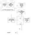
- FIG. 1is a diagram of a system 100 for providing IDDQ variation testing in accordance with an exemplary embodiment of the present invention.
- System 100allows devices such as MOSFETs to be tested to detect defects that standard IDDQ testing might not detect.
- System 100includes VCC test controller 102 , which can be implemented in hardware, software, or a suitable combination of hardware and software, and which can be one or more software systems operating on a suitable processor, such as a general purpose processing platform.
- VCC test controller 102is coupled to voltage vector system 104 and IDDQ measurement system 106 , each of which are coupled to device 112 , which can be a MOSFET, an integrated circuit that includes a plurality of devices including two or more MOSFETs, or other suitable devices.
- VCC testing controller 102is coupled to excitation input system 108 and excitation output system 110 , which are each coupled across the input and output of device 112 , respectively.
- Device 112is also coupled to ground 114 , and voltage vector system 104 , excitation input system 108 and excitation output system 110 can also be coupled to ground 114 or other suitable common voltage reference points.
- Go/no-go system 116 and IDDQ variation monitor 118can be implemented in hardware, software, or a suitable combination of hardware and software, and can be one or more software systems operating on a general purpose processing platform or other suitable processors.
- a software systemcan include one or more objects, agents, threads, line of code, subroutines, separate software applications, two or more lines of code or other suitable software structures operating in two or more separate software applications, on two or more different processors, or other suitable software architectures.
- a software systemcan include one or more lines of code or other suitable software structures operating in a general purpose software application, such as an operating system, and one or more lines of code or other suitable software structures operating in a specific purpose software application.
- Go/no-go system 116is coupled to IDDQ measurement system 106 .
- the term “couple”, and its cognate terms such as “couples” and “coupled”,can include a physical connection (such as through a copper conductor), a virtual connection (such as one or more randomly assigned memory locations of a data memory device), a logical connection (such as through one or more logical devices of a semiconducting circuit), a wireless connection, other suitable connections, or a suitable combination of such connections.
- systems and componentsare coupled to other systems and components through intervening systems and components, such as through an operating system of a general purpose processing platform.
- Go/no-go system 116receives IDDQ current data from IDDQ measurement system 106 and determines whether the IDDQ current exceeds predetermined maximum allowable currents.
- a maximum and minimum range for IDDQcan be determined empirically for device 112 , such that if the measured value of IDDQ current is below the minimum, then the device can be presumed good and defect free from any significant defects.
- the second or maximum IDDQ currentcan be set at a level such that the device can be said to be faulty if the measured value of IDDQ is greater than this level.
- Go/no-go system 116can cause testing of device 112 to be stopped if the measured IDDQ is below the minimum acceptable voltage level, and can initiate testing through IDDQ variation monitor 118 if the voltage is between the minimum and maximum allowable voltages.
- IDDQ variation monitor 118receives voltage vector system 104 outputs and IDDQ measurement system 106 current, and determines whether the change in IDDQ current as a function of voltages applied by voltage vector system 104 indicates potential defects of device 112 .
- applying a power supply voltage and excitation vector to device 112can generate an IDDQ current that includes two basic components.
- the first componentis parasitic diode leakage which is the reverse bias current at the source/drain junctions. All junctions can be biased at either 0.0 volts or VCC, such that the current through IDDQ measurement system 106 remains the same regardless of variations in VCC.
- the second current componentis a subthreshold conduction component. This is the source-to-drain current when transistors are supposed to be shut off. Subthreshold conduction current does not change with changes in VCC.
- IDDQ variation monitor 118generates notification data if variations in IDDQ current measurements as a function of different voltages applied by voltage vector system 104 exceed predetermined allowable variations, such that potential defects are indicated.
- system 100is used to test devices such as MOSFET 112 to determine whether potential defects may exist.
- System 100applies a power supply voltage through voltage vector system 104 to device 112 .
- An excitation voltageis then applied to device 112 and a quiescent IDDQ measurement is obtained.
- the power supply voltageis then varied to determine whether any changes in the quiescent IDDQ current occur. If such changes exceed predetermined allowable variations, then device defects can be inferred.
- System 100can be used in conjunction with existing IDDQ testing, which is based on a “go/no-go paradigm,” where the device 112 is considered acceptable if the IDDQ current is below a predetermined value.
- System 100modifies the “go/no-go paradigm” by adding one or more additional levels at which additional IDDQ variation testing is performed. In this manner, system 100 increases the reliability of IDDQ testing by detecting devices that would otherwise fail after they have been installed in systems or components.
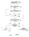
- FIG. 2is a flowchart of a method 200 for performing IDDQ testing in accordance with an exemplary embodiment of the present invention.
- Method 200allows defects and devices to be detected by varying the power supply voltage and determining if changes in IDDQ current or power supply current indicate potential defects.
- Method 200begins at 202 where a voltage vector is provided to excite a fault in a device.
- the voltage vectorcan be applied to the input and output of a MOSFET device or other suitable devices.
- the devicecan also be supplied with a power supply voltage, such as a drain-to-source voltage or other suitable voltages.
- the methodthen proceeds to 204 .
- the quiescence statecan be reached after a predetermined period of time has passed after provision of the excitation vector. Likewise, other quiescence states can be selected. The method then proceeds to 206 .
- the IDDQ as a function of a supply voltage levelis measured.
- the supply voltagecan be increased from a minimum to a maximum at a number of predetermined points.
- Other suitable supply voltage variations sequencescan be used, such as from maximum to minimum, random, in accordance with predetermined sequences, based on previous IDDQ readings and supply voltage settings, or other suitable sequences. The method then proceeds to 208 .
- the maximum numbercan be predetermined, can be a function of the variation measured in previous steps, or other suitable procedures can be used. If the number of measurements if less than the maximum, then the method returns to 206 . Otherwise, the method proceeds to 210 .
- the variation in the IDDQis determined.
- statistical analysiscan be applied to the measurement points to determine mean variations, maximum variations, median variations, variation trends, or other suitable variations. The method then proceeds to 212 .
- nominal variationscan be determined empirically by testing large numbers of devices, can be determined in accordance with calculated nominal variations for acceptable device variations, or other suitable nominal variations can be used. If it is determined at 212 that the variation is not greater than nominal, the method proceeds to 214 where the device is accepted. Otherwise, the method proceeds to 216 where notification data is generated.
- the notification datacan include a report entry for the device that can be scanned after completion of testing of all devices. Likewise, robotic control data can be generated to remove the device from testing or to mark the device as failed, an operator can be notified, or other suitable notification data can be generated.
- method 200allows devices to be tested to detect faults.
- the devicescan include MOSFET devices where the IDDQ current is measured as a function of changes in supply voltage. If the variations in IDDQ are greater than predetermined nominal variations, then it can be inferred that a defect in the device may cause the device to fail.
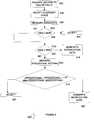
- FIG. 3is a flowchart of a method 300 for performing two stages of IDDQ testing in accordance with an exemplary embodiment of the present invention.
- Method 300allows multiple IDDQ acceptance levels to be set such that if IDDQ is below predetermined values then devices are accepted without performing additional IDDQ testing, such as where a large number of devices are being tested and it is desired to decrease the amount of time for testing each device.
- Method 300begins at 302 where a vector is applied to a device to excite a fault.
- the vectorcan be applied to an input and output of the device after the device has been subjected to a power supply voltage, or the device can be tested without power supply voltage. The method then proceeds to 304 .
- a quiescent stateis selected for the device.
- the quiescent statecan be determined by a predetermined period of time, by predetermined length of times and changes, or in accordance with other suitable procedures. The method then proceeds to 306 .
- an IDDQis measured at a first measurement point.
- the first measurement pointcan be based on device operating power supply voltages, maximum test overvoltages, or other suitable voltages. The method then proceeds to 308 .
- the methodproceeds to 310 and the device is accepted. Otherwise, the method proceeds to 312 .
- IDDQ at a different power supply voltage levelis measured.
- the voltagecan be changed as a function of a predetermined sequence of increasing or decreasing steps, at random sequence, based on prior measurements, or other suitable selection criteria.
- the methodthen proceeds to 314 where it is determined whether all steps have been measured. If the number of steps does not equal the maximum number, the method returns to 312 . Otherwise, the method proceeds to 316 .
- the variation in IDDQis determined, such as by determining the maximum variation, the mean variation, the median variation, variation trends, or other suitable variations. The method then proceeds to 318 .
- the methodproceeds to 320 where the device is accepted. Otherwise, the method proceeds to 322 where notification data is generated.
- method 300allows devices to be tested in a two-stage process, where a first level is determined for power supply current. If the first level is not exceeded, then the device is accepted. Otherwise, a second level of testing is performed where variations of power supply current as a function of power supply voltage are determined. If these variations do not exceed nominal values for variations, then the device is accepted. Otherwise, the device is rejected.
- FIG. 4is a flowchart of a method 400 for performing IDDQ testing in accordance with an exemplary embodiment of the present invention.
- Method 400allows IDDQ measurements at various voltages to be used to determine whether the device is acceptable.
- Method 400begins at 402 where a power supply voltage is applied to a device and an excitation vector is applied to excite a fault.
- the power supply voltagecan vary from zero to in excess of operating levels, and the excitation fault vector can include one or more voltage levels that the device may be exposed to during operation up to a maximum design level.
- the methodthen proceeds to 404 .
- a quiescent stateis selected.
- the quiescent statecan include a predetermined period of time, predetermined changes, or other suitable quiescent states. The method then proceeds to 406 .
- IDDQ at a first voltage levelis measured.
- the first voltagecan be the operating voltage level, a design maximum level, or other suitable levels.
- the methodthen proceeds to 408 .
- the methodproceeds to 414 where notification data is generated.
- the notification datacan include data that causes the device to be removed from testing, that notifies an operator, that causes a mark to be applied to the device, or other suitable notification data can be generated. The method then proceeds to 416 .
- the variation in IDDQis determined, such as by determining the maximum variation, the mean variation, the median variation, variation trends, or other suitable variations. The method then proceeds to 418 .
- method 400allows devices to be tested in a two-stage process, where a first level is determined for power supply current. If the first level is not exceeded, then the device is accepted. Otherwise, a second level of testing is performed where variations of power supply current as a function of power supply voltage are determined. If these variations do not exceed nominal values for variations, then the device is accepted. Otherwise, the device is rejected.
- FIG. 5is a flowchart of a method 500 for performing IDDQ testing in accordance with an exemplary embodiment of the present invention.
- Method 500is a special case of method 400 with measurement points only taken in the final stage.
- Method 500begins at 502 where a power supply voltage is applied to a device and an excitation vector is applied to excite a fault.
- the power supply voltagecan vary from zero to in excess of operating levels, and the excitation fault vector can include one or more voltage levels that the device may be exposed to during operation up to a maximum design level.
- the methodthen proceeds to 504 .
- a quiescent stateis selected.
- the quiescent statecan include a predetermined period of time, predetermined changes, or other suitable quiescent states. The method then proceeds to 506 .
- IDDQ at a first voltage levelis measured.
- the first voltagecan be the operating voltage level, a design maximum level, or other suitable levels.
- the methodthen proceeds to 508 .
- the methodproceeds to 514 where notification data is generated.
- the notification datacan include data that causes the device to be removed from testing, that notifies an operator, that causes a mark to be applied to the device, or other suitable notification data can be generated. The method then proceeds to 516 .
- the IDDQ at a power supply maximum and minimumis determined.
- the maximumcan be an operating voltage level or a design maximum
- the minimumcan be zero, a negative voltage, or other suitable voltages. The method then proceeds to 518 .
- the absolute value of the difference between the IDDQ at the maximum and minimum levelsis divided by the minimum of either of those two values and it is determined whether that value is less than a predetermined value. If the value is less than a predetermined value, which can be determined empirically, the method proceeds to 520 and the device is accepted. Otherwise, the method proceeds to 522 and notification data is generated.
- method 500provides an IDDQ testing procedure that allows devices with defects to be detected that would otherwise pass a go/no-go test.
- Method 500identifies a range of acceptable IDDQ values and performs additional testing to detect devices with failure modes that would not be determined otherwise.
Landscapes
- Engineering & Computer Science (AREA)
- General Engineering & Computer Science (AREA)
- Physics & Mathematics (AREA)
- General Physics & Mathematics (AREA)
- Testing Of Individual Semiconductor Devices (AREA)
- Tests Of Electronic Circuits (AREA)
Abstract
Description
| Id = | W/L*Ido*exp[−Vbs(1/nVt) − (1/Vt)]*[1 − exp(−Vds/Vt)]*exp |
| [(Vgs − Vth)/(nVt)] | |
| where | |
| Id = | drain current |
| Vt = | thermal voltage (KT/q) |
| Vth = | threshold voltage |
| Vds = | drain-to-source voltage >> Vt (Vt = kT/q ˜ 25 mv, Vds ˜ VCC) |
| Vbs = | bulk-to-source voltage = 0 (bulk potential = source potential) |
| Vgs = | gate-to-source voltage |
| Ido = | constant |
| W = | width of MOS transistor |
| L = | length of MOS transistor |
Claims (4)
Priority Applications (2)
| Application Number | Priority Date | Filing Date | Title |
|---|---|---|---|
| US09/862,045US6664801B1 (en) | 2001-05-21 | 2001-05-21 | IDDQ test methodology based on the sensitivity of fault current to power supply variations |
| US10/684,119US6842032B2 (en) | 2001-05-21 | 2003-10-10 | IDDQ test methodology based on the sensitivity of fault current to power supply variations |
Applications Claiming Priority (1)
| Application Number | Priority Date | Filing Date | Title |
|---|---|---|---|
| US09/862,045US6664801B1 (en) | 2001-05-21 | 2001-05-21 | IDDQ test methodology based on the sensitivity of fault current to power supply variations |
Related Child Applications (1)
| Application Number | Title | Priority Date | Filing Date |
|---|---|---|---|
| US10/684,119DivisionUS6842032B2 (en) | 2001-05-21 | 2003-10-10 | IDDQ test methodology based on the sensitivity of fault current to power supply variations |
Publications (1)
| Publication Number | Publication Date |
|---|---|
| US6664801B1true US6664801B1 (en) | 2003-12-16 |
Family
ID=29712668
Family Applications (2)
| Application Number | Title | Priority Date | Filing Date |
|---|---|---|---|
| US09/862,045Expired - LifetimeUS6664801B1 (en) | 2001-05-21 | 2001-05-21 | IDDQ test methodology based on the sensitivity of fault current to power supply variations |
| US10/684,119Expired - Fee RelatedUS6842032B2 (en) | 2001-05-21 | 2003-10-10 | IDDQ test methodology based on the sensitivity of fault current to power supply variations |
Family Applications After (1)
| Application Number | Title | Priority Date | Filing Date |
|---|---|---|---|
| US10/684,119Expired - Fee RelatedUS6842032B2 (en) | 2001-05-21 | 2003-10-10 | IDDQ test methodology based on the sensitivity of fault current to power supply variations |
Country Status (1)
| Country | Link |
|---|---|
| US (2) | US6664801B1 (en) |
Cited By (9)
| Publication number | Priority date | Publication date | Assignee | Title |
|---|---|---|---|---|
| US20040012397A1 (en)* | 1998-09-09 | 2004-01-22 | Hitachi, Ltd. | Semiconductor integrated circuit apparatus |
| US20040046576A1 (en)* | 2002-07-03 | 2004-03-11 | Q-Star Test N.V. | Device for monitoring quiescent current of an electronic device |
| US20040263201A1 (en)* | 2003-04-09 | 2004-12-30 | Infineon Technologies Ag | Method and apparatus for determining the switching state of a transistor |
| WO2005047911A1 (en)* | 2003-11-05 | 2005-05-26 | International Business Machines Corporation | Hot switchable voltage bus for iddq current measurements |
| US20100320997A1 (en)* | 2009-06-19 | 2010-12-23 | Mcquirk Dale J | Method and circuit for measuring quiescent current |
| US20110107797A1 (en)* | 2008-07-18 | 2011-05-12 | Shin-Etsu Chemical Co., Ltd. | Optical fiber preform manufacturing method and optical fiber preform manufacturing device |
| US20140007624A1 (en)* | 2009-03-30 | 2014-01-09 | Toyo Seikan Group Holdings, Ltd. | Method for controlling diameter of grin lens fiber and fiber drawing equipment |
| US20140318188A1 (en)* | 2013-04-30 | 2014-10-30 | Corning Incorporated | Methods for modifying multi-mode optical fiber manufacturing processes |
| US11698485B2 (en) | 2020-01-03 | 2023-07-11 | Corning Incorporated | Method for manufacturing multimode optical fibers |
Families Citing this family (2)
| Publication number | Priority date | Publication date | Assignee | Title |
|---|---|---|---|---|
| US7373561B2 (en)* | 2002-10-29 | 2008-05-13 | Broadcom Corporation | Integrated packet bit error rate tester for 10G SERDES |
| US8044676B2 (en)* | 2008-06-11 | 2011-10-25 | Infineon Technologies Ag | IDDQ testing |
Citations (2)
| Publication number | Priority date | Publication date | Assignee | Title |
|---|---|---|---|---|
| US5731700A (en)* | 1994-03-14 | 1998-03-24 | Lsi Logic Corporation | Quiescent power supply current test method and apparatus for integrated circuits |
| US6118293A (en)* | 1996-06-05 | 2000-09-12 | Imec Inter Uni Micro Electr | High resolution (quiescent) supply current system (IDD monitor) |
- 2001
- 2001-05-21USUS09/862,045patent/US6664801B1/ennot_activeExpired - Lifetime
- 2003
- 2003-10-10USUS10/684,119patent/US6842032B2/ennot_activeExpired - Fee Related
Patent Citations (2)
| Publication number | Priority date | Publication date | Assignee | Title |
|---|---|---|---|---|
| US5731700A (en)* | 1994-03-14 | 1998-03-24 | Lsi Logic Corporation | Quiescent power supply current test method and apparatus for integrated circuits |
| US6118293A (en)* | 1996-06-05 | 2000-09-12 | Imec Inter Uni Micro Electr | High resolution (quiescent) supply current system (IDD monitor) |
Cited By (19)
| Publication number | Priority date | Publication date | Assignee | Title |
|---|---|---|---|---|
| US6946865B2 (en)* | 1998-09-09 | 2005-09-20 | Renesas Technology Corporation | Semiconductor integrated circuit apparatus |
| US20040012397A1 (en)* | 1998-09-09 | 2004-01-22 | Hitachi, Ltd. | Semiconductor integrated circuit apparatus |
| US7315180B2 (en) | 2002-07-03 | 2008-01-01 | Q-Star Test N.V. | Device for monitoring quiescent current of an electronic device |
| US20050156619A1 (en)* | 2002-07-03 | 2005-07-21 | Q-Star Test N.V. | Device for monitoring quiescent current of an electronic device |
| US6927592B2 (en)* | 2002-07-03 | 2005-08-09 | Q-Star Test N.V. | Device for monitoring quiescent current of an electronic device |
| US20040046576A1 (en)* | 2002-07-03 | 2004-03-11 | Q-Star Test N.V. | Device for monitoring quiescent current of an electronic device |
| US20040263201A1 (en)* | 2003-04-09 | 2004-12-30 | Infineon Technologies Ag | Method and apparatus for determining the switching state of a transistor |
| US7005882B2 (en)* | 2003-04-09 | 2006-02-28 | Infineon Technologies Ag | Method and apparatus for determining the switching state of a transistor |
| WO2005047911A1 (en)* | 2003-11-05 | 2005-05-26 | International Business Machines Corporation | Hot switchable voltage bus for iddq current measurements |
| US20080129324A1 (en)* | 2003-11-05 | 2008-06-05 | International Business Machines Corporation | Hot Switchable Voltage Bus for Iddq Current Measurements |
| US20110107797A1 (en)* | 2008-07-18 | 2011-05-12 | Shin-Etsu Chemical Co., Ltd. | Optical fiber preform manufacturing method and optical fiber preform manufacturing device |
| US10501361B2 (en)* | 2008-07-18 | 2019-12-10 | Shin-Etsu Chemical Co., Ltd. | Optical fiber preform manufacturing method and optical fiber preform manufacturing device |
| US20140007624A1 (en)* | 2009-03-30 | 2014-01-09 | Toyo Seikan Group Holdings, Ltd. | Method for controlling diameter of grin lens fiber and fiber drawing equipment |
| US20100320997A1 (en)* | 2009-06-19 | 2010-12-23 | Mcquirk Dale J | Method and circuit for measuring quiescent current |
| US8278960B2 (en)* | 2009-06-19 | 2012-10-02 | Freescale Semiconductor, Inc. | Method and circuit for measuring quiescent current |
| US20140318188A1 (en)* | 2013-04-30 | 2014-10-30 | Corning Incorporated | Methods for modifying multi-mode optical fiber manufacturing processes |
| US10131566B2 (en)* | 2013-04-30 | 2018-11-20 | Corning Incorporated | Methods for modifying multi-mode optical fiber manufacturing processes |
| US11708291B2 (en) | 2013-04-30 | 2023-07-25 | Corning Incorporated | Methods for modifying multi-mode optical fiber manufacturing processes |
| US11698485B2 (en) | 2020-01-03 | 2023-07-11 | Corning Incorporated | Method for manufacturing multimode optical fibers |
Also Published As
| Publication number | Publication date |
|---|---|
| US6842032B2 (en) | 2005-01-11 |
| US20040080331A1 (en) | 2004-04-29 |
Similar Documents
| Publication | Publication Date | Title |
|---|---|---|
| US6476632B1 (en) | Ring oscillator design for MOSFET device reliability investigations and its use for in-line monitoring | |
| US5332973A (en) | Built-in fault testing of integrated circuits | |
| US7589550B2 (en) | Semiconductor device test system having reduced current leakage | |
| US6664801B1 (en) | IDDQ test methodology based on the sensitivity of fault current to power supply variations | |
| JP3660561B2 (en) | Failure analysis device for semiconductor integrated circuit | |
| US7649376B2 (en) | Semiconductor device including test element group and method for testing therefor | |
| US8362794B2 (en) | Method and system for assessing reliability of integrated circuit | |
| US6144214A (en) | Method and apparatus for use in IDDQ integrated circuit testing | |
| US5365180A (en) | Method for measuring contact resistance | |
| US20100315114A1 (en) | Semiconductor device with test structure and semiconductor device test method | |
| JP4507379B2 (en) | Non-defective product judgment method for CMOS integrated circuit | |
| US20050156605A1 (en) | Circuits for transistor testing | |
| JP6348755B2 (en) | Method for testing semiconductor transistors | |
| JP2008078266A (en) | Semiconductor device, characteristic measurement method for device under test, and characteristic management system for semiconductor device | |
| US20160146879A1 (en) | Methods, apparatus and system for voltage ramp testing | |
| Kruseman et al. | The future of delta I/sub DDQ/testing | |
| US20030193051A1 (en) | Measuring junction leakage | |
| KR100648260B1 (en) | Semiconductor wafer with magnetic shielding function and test method thereof | |
| US7332924B2 (en) | Embedded test circuitry and a method for testing a semiconductor device for breakdown, wearout or failure | |
| US11327112B2 (en) | Semiconductor device for detecting characteristics of semiconductor element and operating method thereof | |
| KR20060022287A (en) | Analog or radio frequency circuit testing methods, apparatus and recording media | |
| US6737671B2 (en) | Current measurement circuit and method for voltage regulated semiconductor integrated circuit devices | |
| JP2014163851A (en) | Semiconductor integrated circuit with open detection terminal | |
| JP3372488B2 (en) | Test device for semiconductor CMOS integrated circuit | |
| JP2907278B2 (en) | Semiconductor device and test method thereof |
Legal Events
| Date | Code | Title | Description |
|---|---|---|---|
| AS | Assignment | Owner name:LSI LOGIC CORPORATION, CALIFORNIA Free format text:ASSIGNMENT OF ASSIGNORS INTEREST;ASSIGNOR:PALUSA, CHAITANYA;REEL/FRAME:011877/0851 Effective date:20010514 | |
| FEPP | Fee payment procedure | Free format text:PAYOR NUMBER ASSIGNED (ORIGINAL EVENT CODE: ASPN); ENTITY STATUS OF PATENT OWNER: LARGE ENTITY Free format text:PAYER NUMBER DE-ASSIGNED (ORIGINAL EVENT CODE: RMPN); ENTITY STATUS OF PATENT OWNER: LARGE ENTITY | |
| STCF | Information on status: patent grant | Free format text:PATENTED CASE | |
| FPAY | Fee payment | Year of fee payment:4 | |
| FEPP | Fee payment procedure | Free format text:PAYOR NUMBER ASSIGNED (ORIGINAL EVENT CODE: ASPN); ENTITY STATUS OF PATENT OWNER: LARGE ENTITY Free format text:PAYER NUMBER DE-ASSIGNED (ORIGINAL EVENT CODE: RMPN); ENTITY STATUS OF PATENT OWNER: LARGE ENTITY | |
| FPAY | Fee payment | Year of fee payment:8 | |
| AS | Assignment | Owner name:DEUTSCHE BANK AG NEW YORK BRANCH, AS COLLATERAL AG Free format text:PATENT SECURITY AGREEMENT;ASSIGNORS:LSI CORPORATION;AGERE SYSTEMS LLC;REEL/FRAME:032856/0031 Effective date:20140506 | |
| AS | Assignment | Owner name:LSI CORPORATION, CALIFORNIA Free format text:CHANGE OF NAME;ASSIGNOR:LSI LOGIC CORPORATION;REEL/FRAME:033102/0270 Effective date:20070406 | |
| AS | Assignment | Owner name:AVAGO TECHNOLOGIES GENERAL IP (SINGAPORE) PTE. LTD Free format text:ASSIGNMENT OF ASSIGNORS INTEREST;ASSIGNOR:LSI CORPORATION;REEL/FRAME:035390/0388 Effective date:20140814 | |
| FPAY | Fee payment | Year of fee payment:12 | |
| AS | Assignment | Owner name:LSI CORPORATION, CALIFORNIA Free format text:TERMINATION AND RELEASE OF SECURITY INTEREST IN PATENT RIGHTS (RELEASES RF 032856-0031);ASSIGNOR:DEUTSCHE BANK AG NEW YORK BRANCH, AS COLLATERAL AGENT;REEL/FRAME:037684/0039 Effective date:20160201 Owner name:AGERE SYSTEMS LLC, PENNSYLVANIA Free format text:TERMINATION AND RELEASE OF SECURITY INTEREST IN PATENT RIGHTS (RELEASES RF 032856-0031);ASSIGNOR:DEUTSCHE BANK AG NEW YORK BRANCH, AS COLLATERAL AGENT;REEL/FRAME:037684/0039 Effective date:20160201 | |
| AS | Assignment | Owner name:BANK OF AMERICA, N.A., AS COLLATERAL AGENT, NORTH CAROLINA Free format text:PATENT SECURITY AGREEMENT;ASSIGNOR:AVAGO TECHNOLOGIES GENERAL IP (SINGAPORE) PTE. LTD.;REEL/FRAME:037808/0001 Effective date:20160201 Owner name:BANK OF AMERICA, N.A., AS COLLATERAL AGENT, NORTH Free format text:PATENT SECURITY AGREEMENT;ASSIGNOR:AVAGO TECHNOLOGIES GENERAL IP (SINGAPORE) PTE. LTD.;REEL/FRAME:037808/0001 Effective date:20160201 | |
| AS | Assignment | Owner name:AVAGO TECHNOLOGIES GENERAL IP (SINGAPORE) PTE. LTD., SINGAPORE Free format text:TERMINATION AND RELEASE OF SECURITY INTEREST IN PATENTS;ASSIGNOR:BANK OF AMERICA, N.A., AS COLLATERAL AGENT;REEL/FRAME:041710/0001 Effective date:20170119 Owner name:AVAGO TECHNOLOGIES GENERAL IP (SINGAPORE) PTE. LTD Free format text:TERMINATION AND RELEASE OF SECURITY INTEREST IN PATENTS;ASSIGNOR:BANK OF AMERICA, N.A., AS COLLATERAL AGENT;REEL/FRAME:041710/0001 Effective date:20170119 | |
| AS | Assignment | Owner name:BELL SEMICONDUCTOR, LLC, ILLINOIS Free format text:ASSIGNMENT OF ASSIGNORS INTEREST;ASSIGNORS:AVAGO TECHNOLOGIES GENERAL IP (SINGAPORE) PTE. LTD.;BROADCOM CORPORATION;REEL/FRAME:044887/0109 Effective date:20171208 | |
| AS | Assignment | Owner name:CORTLAND CAPITAL MARKET SERVICES LLC, AS COLLATERA Free format text:SECURITY INTEREST;ASSIGNORS:HILCO PATENT ACQUISITION 56, LLC;BELL SEMICONDUCTOR, LLC;BELL NORTHERN RESEARCH, LLC;REEL/FRAME:045216/0020 Effective date:20180124 | |
| AS | Assignment | Owner name:BELL NORTHERN RESEARCH, LLC, ILLINOIS Free format text:RELEASE BY SECURED PARTY;ASSIGNOR:CORTLAND CAPITAL MARKET SERVICES LLC;REEL/FRAME:059720/0223 Effective date:20220401 Owner name:BELL SEMICONDUCTOR, LLC, ILLINOIS Free format text:RELEASE BY SECURED PARTY;ASSIGNOR:CORTLAND CAPITAL MARKET SERVICES LLC;REEL/FRAME:059720/0223 Effective date:20220401 Owner name:HILCO PATENT ACQUISITION 56, LLC, ILLINOIS Free format text:RELEASE BY SECURED PARTY;ASSIGNOR:CORTLAND CAPITAL MARKET SERVICES LLC;REEL/FRAME:059720/0223 Effective date:20220401 |