US6664582B2 - Fin memory cell and method of fabrication - Google Patents
Fin memory cell and method of fabricationDownload PDFInfo
- Publication number
- US6664582B2 US6664582B2US10/063,330US6333002AUS6664582B2US 6664582 B2US6664582 B2US 6664582B2US 6333002 AUS6333002 AUS 6333002AUS 6664582 B2US6664582 B2US 6664582B2
- Authority
- US
- United States
- Prior art keywords
- fin body
- fin
- memory cell
- capacitor
- forming
- Prior art date
- Legal status (The legal status is an assumption and is not a legal conclusion. Google has not performed a legal analysis and makes no representation as to the accuracy of the status listed.)
- Expired - Lifetime
Links
Images


Classifications
- H—ELECTRICITY
- H10—SEMICONDUCTOR DEVICES; ELECTRIC SOLID-STATE DEVICES NOT OTHERWISE PROVIDED FOR
- H10B—ELECTRONIC MEMORY DEVICES
- H10B12/00—Dynamic random access memory [DRAM] devices
- H10B12/30—DRAM devices comprising one-transistor - one-capacitor [1T-1C] memory cells
- H10B12/39—DRAM devices comprising one-transistor - one-capacitor [1T-1C] memory cells the capacitor and the transistor being in a same trench
- H—ELECTRICITY
- H10—SEMICONDUCTOR DEVICES; ELECTRIC SOLID-STATE DEVICES NOT OTHERWISE PROVIDED FOR
- H10B—ELECTRONIC MEMORY DEVICES
- H10B12/00—Dynamic random access memory [DRAM] devices
- H10B12/01—Manufacture or treatment
- H10B12/02—Manufacture or treatment for one transistor one-capacitor [1T-1C] memory cells
- H10B12/05—Making the transistor
- H10B12/053—Making the transistor the transistor being at least partially in a trench in the substrate
- H—ELECTRICITY
- H10—SEMICONDUCTOR DEVICES; ELECTRIC SOLID-STATE DEVICES NOT OTHERWISE PROVIDED FOR
- H10B—ELECTRONIC MEMORY DEVICES
- H10B12/00—Dynamic random access memory [DRAM] devices
- H10B12/01—Manufacture or treatment
- H10B12/02—Manufacture or treatment for one transistor one-capacitor [1T-1C] memory cells
- H10B12/05—Making the transistor
- H10B12/056—Making the transistor the transistor being a FinFET
- H—ELECTRICITY
- H10—SEMICONDUCTOR DEVICES; ELECTRIC SOLID-STATE DEVICES NOT OTHERWISE PROVIDED FOR
- H10D—INORGANIC ELECTRIC SEMICONDUCTOR DEVICES
- H10D86/00—Integrated devices formed in or on insulating or conducting substrates, e.g. formed in silicon-on-insulator [SOI] substrates or on stainless steel or glass substrates
- H10D86/01—Manufacture or treatment
- H10D86/011—Manufacture or treatment comprising FinFETs
- H—ELECTRICITY
- H10—SEMICONDUCTOR DEVICES; ELECTRIC SOLID-STATE DEVICES NOT OTHERWISE PROVIDED FOR
- H10D—INORGANIC ELECTRIC SEMICONDUCTOR DEVICES
- H10D86/00—Integrated devices formed in or on insulating or conducting substrates, e.g. formed in silicon-on-insulator [SOI] substrates or on stainless steel or glass substrates
- H10D86/201—Integrated devices formed in or on insulating or conducting substrates, e.g. formed in silicon-on-insulator [SOI] substrates or on stainless steel or glass substrates the substrates comprising an insulating layer on a semiconductor body, e.g. SOI
- H10D86/215—Integrated devices formed in or on insulating or conducting substrates, e.g. formed in silicon-on-insulator [SOI] substrates or on stainless steel or glass substrates the substrates comprising an insulating layer on a semiconductor body, e.g. SOI comprising FinFETs
- H—ELECTRICITY
- H10—SEMICONDUCTOR DEVICES; ELECTRIC SOLID-STATE DEVICES NOT OTHERWISE PROVIDED FOR
- H10B—ELECTRONIC MEMORY DEVICES
- H10B12/00—Dynamic random access memory [DRAM] devices
- H10B12/30—DRAM devices comprising one-transistor - one-capacitor [1T-1C] memory cells
- H10B12/48—Data lines or contacts therefor
- H10B12/485—Bit line contacts
- H—ELECTRICITY
- H10—SEMICONDUCTOR DEVICES; ELECTRIC SOLID-STATE DEVICES NOT OTHERWISE PROVIDED FOR
- H10D—INORGANIC ELECTRIC SEMICONDUCTOR DEVICES
- H10D30/00—Field-effect transistors [FET]
- H10D30/01—Manufacture or treatment
- H10D30/021—Manufacture or treatment of FETs having insulated gates [IGFET]
- H10D30/024—Manufacture or treatment of FETs having insulated gates [IGFET] of fin field-effect transistors [FinFET]
- H—ELECTRICITY
- H10—SEMICONDUCTOR DEVICES; ELECTRIC SOLID-STATE DEVICES NOT OTHERWISE PROVIDED FOR
- H10D—INORGANIC ELECTRIC SEMICONDUCTOR DEVICES
- H10D30/00—Field-effect transistors [FET]
- H10D30/60—Insulated-gate field-effect transistors [IGFET]
- H10D30/62—Fin field-effect transistors [FinFET]
- H—ELECTRICITY
- H10—SEMICONDUCTOR DEVICES; ELECTRIC SOLID-STATE DEVICES NOT OTHERWISE PROVIDED FOR
- H10D—INORGANIC ELECTRIC SEMICONDUCTOR DEVICES
- H10D89/00—Aspects of integrated devices not covered by groups H10D84/00 - H10D88/00
- H10D89/10—Integrated device layouts
Definitions
- the present inventionrelates generally to the field of semiconductor manufacturing and, more specifically, to a method for forming double gated field effect transistors.
- DRAMDynamic Random Access Memory
- ASICsapplication specific integrated circuits
- Each DRAM cellcontains an access transistor and a capacitor used to store the memory data.
- the two most common types of capacitors used to store the memoryare deep trench and planar capacitors.
- Deep trench capacitorsgenerally have the advantage of increased memory density, but have the disadvantage of increased process complexity and cost. For this reason, deep trench capacitors are generally only used where the large number of memory cells can justify the increased process cost.
- planar capacitorscan be manufactured using much simpler manufacturing techniques, and generally do not add excessive processing costs to the device.
- planar capacitorsdo not provide the cell density that deep trench capacitors do, and thus are limited to applications in which the number of memory cells needed is relatively low.
- the present inventionprovides a memory cell and method for forming the same that results in improved cell density without overly increasing fabrication cost and complexity.
- the preferred embodiment of the present inventionprovides a fin design to form the memory cell. Specifically, a fin Field Effect Transistor (FET) is formed to provide the access transistor, and a fin capacitor is formed to provide the storage capacitor.
- FETfin Field Effect Transistor
- the memory cell densitycan be greatly increased over traditional planar capacitor designs. Additionally, the memory cell can be formed with significantly less process cost and complexity than traditional deep trench capacitor designs.
- FIG. 1is a flow diagram illustrating a first fabrication method
- FIGS. 4, 7 , 8 , 10 , 11 and 13are top views of an exemplary memory device during fabrication.
- the present inventionprovides a memory cell and method for forming the same that results in improved cell density without overly increasing fabrication cost and complexity.
- the preferred embodiment of the present inventionuses a fin design to form the memory cell. Specifically, a fin Field Effect Transistor (FET) is formed to provide the access transistor, and a fin capacitor is formed to provide the storage capacitor.
- FETfin Field Effect Transistor
- the memory cell densitycan be greatly increased over traditional planar capacitor designs. Additionally, the memory cell can be formed with significantly less process cost and complexity than traditional deep trench capacitor designs.
- the body of the transistoris formed with a vertical “fin” shape.
- the gates of the transistorare then formed on one or more sides of the fin.
- the preferred method for forming this double gated transistorsallows the gate length of the device to have minimum feature size, while allowing the thickness of the body to be much smaller than the gate length.
- the preferred method for forming the fin FETaccomplishes this by using an image enhancement technique, sidewall image transfer, to define the thickness of the transistor body, allowing it to be reliably formed at sub minimum feature size.
- the memory cell of the current inventionalso forms the storage capacitor using the fin shaped body. Specifically, a portion of the fin body will be highly doped and made to comprise the storage node of the memory cell capacitor. An insulator layer is then formed on the fin sidewalls, and a common counter electrode is formed over the fins to complete the fin capacitor. These fin capacitors have the advantage of providing a high device density without requiring excessive process complexity.
- the memory cell of the current inventionhas density advantages over typical planar memory cells for several reasons.
- Second, the fin structure of the capacitorallows for greater capacitance in a limited space than can be accomplished using typical planar capacitor technology. This is because both sides of the fin comprise capacitor storage area. Fins are typically formed one lithographic unit high and thus the fin capacitor can have twice the capacitor storage area of the typical planar capacitor. Further advantage yet is attainable through the use of taller fins to obtain greater storage capacitance without any penalty to the physical cell area. Taken together, a fin memory cell can thus be formed in less than ten lithographic squares, depending upon the area allocated to the fin capacitor. For example, if the capacitor is limited in width to the minimum feature size, the memory cell can be formed in nine lithographic squares.
- the typical planar DRAM cellmust be at least 25% larger for equivalent lithographic feature size. This is because silicon mesas used to form the FET and the storage node must be at least on lithographic square wide, and hence the entire cell must grow to accommodate this size. Even with the increase in layout area, the typical planar DRAM cell will have half the capacitance of the fin memory cell because of the added capacitance of the fin capacitor discussed above. In contrast, in typical planar cells the cell area must be increased to increase the storage area.
- the fin memory cellcan provide high density memory arrays for storage used in embedded applications at low process cost.
- the first step 102 of method 100is to provide an appropriate wafer.
- the wafer usedcomprises a silicon on insulator (SOI) wafer.
- the waferis comprised of a buried oxide layer beneath an SOI layer.
- the SOI layeris used to form the body of the double gated transistor.
- the doping of the SOI layeris done later with an appropriate implant.
- non-SOI waferscan be used.
- the processingremains otherwise identical to those of the SOI wafer case, except as noted.
- the next step 104 of method 100is to form a fin pattern using sidewall image transfer. It is generally desirable to have the fin thickness narrower than the gate length. Typically, the fin thickness should be less than one quarter of the gate length to give good threshold voltage control. Also, it is generally desirable that the fin thickness should be greater than 2.5 nm to avoid degraded mobility due to quantum confinement issues. As the gate length is generally made to minimum feature size, sidewall image transfer is used to achieve the subminimum feature size of the fin.
- Sidewall image transfertypically involves the formation of a mandrel layer and at least one etch stop layer.
- the mandrel layeris then patterned, and sidewall spacers are formed on the sidewalls of the patterned mandrel layer.
- These sidewall spacerswill be used to define the fins, completing the sidewall image transfer.
- Sidewall image transferprovides many advantages, the most notable being that it allows features to be accurately fabricated below the minimum lithographic feature size. Specifically, because sidewall image transfer is used to define the fins, the fins of the transistor can be accurately formed with a narrower width than could be formed using traditional lithography.
- the fin widthis determined by the spacer width. Spacer width can be etched much narrower than the fin can be printed and formed using conventional lithography.
- the mandrel layeris thus first patterned to define shapes such that the exterior perimeter of the shapes will provide the sidewalls used to define the spacers.
- the mandrel layerpreferably comprises a layer of oxide or other suitable material. Generally it will be desirable for the mandrel layer to have a thickness of between 10 nm and 100 nm, however, such a thickness may change depending on the desired body thickness.
- the sidewall spacercan be formed using a deposition of silicon nitride or other suitable material, followed by a suitable directional etch.
- FIG. 2a cross sectional view of a wafer portion 200 is illustrated after the formation of an etch stop layers and a mandrel layer.
- the wafer portion 200comprises an SOI wafer, and as such includes an. SOI layer 202 and a buried insulator layer 204 . On top of the SOI layer is formed an etch stop layer. On top of etch stop layer 206 is formed a mandrel layer 212 .
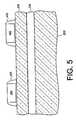
- FIG. 5a cross sectional view of wafer portion 200 is illustrated after the formation of sidewall spacers 403 on the sidewalls of mandrel shapes 402 .
- FIG. 6a cross sectional view of wafer portion 200 is illustrated after the mandrel shapes 402 and etch stop layer 206 have been removed, leaving only a loop of sidewall spacer 403 around the old perimeter of the mandrel shapes. Because this process has naturally formed sidewall spacers on all edges of the mandrel shapes, the sidewall spacers will generally comprise “loops” of material. As will be described next, these loops will be trimmed to provide for discrete fin structures.
- the next step 106is to trim the fin pattern.
- the fin patternis trimmed to turn the loops into discrete shapes. Specifically, the ends of each fin pattern loop are removed, making two fin patterns from each loop. This can be done using any suitable patterning technique, such as depositing and patterning a suitable photoresist to expose only the ends of the loops, and then etching away the exposed ends. The remaining photoresist is then stripped, leaving the discrete fin patterns.
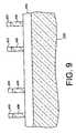
- FIG. 9a cross sectional view of wafer portion 200 is illustrated after the fins and have been formed. Specifically, a fin 406 is formed from the SOI layer under each of the sidewall spacers 403 that made up the fin pattern. In the case where bulk wafers are used, etch stop is performed by other means, such as form layer or a timed etch to desired depth.
- next step 110is to form sacrificial oxide on the sidewalls of the fin.
- Sacrificial oxideis used to clean the exposed sides of the fins and protect the fins during ion implantation.
- the sacrificial oxidewould be provided by growing a thin layer of thermal oxide.
- additional processing on the exposed capacitor portions 412 (see FIG. 10) of the finscan be performed using additional or different types of dielectric, such as high k dielectric 415 (see FIG. 14, can be formed only on the capacitor portions 412 of the fins at this time.
- Other processing of the exposed capacitor portions 412 of the finscould include adding additional conductive material to improve the performance of the capacitor or to give improved process capability with the capacitor dielectric 415 .
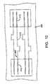
- FIG. 10a top view of wafer portion 200 is showing how the fins 406 are selectively exposed during a dopant implant process. This degenerately dopes the capacitor portions 412 of the fins 406 , while leaving other portions 413 of the fins 406 undoped. These highly doped portions of the fins 406 will be used to form the storage nodes of the memory cell capacitors. Again, other processing, such as the formation of special capacitor dielectrics can be performed at this time.
- next step 114is to perform additional fin implants and remove the sacrificial oxide.
- additional implantswith the appropriate species (depending on whether N-type or p-type transistors are being formed) are made into the fin body. These implants can be performed to properly dope the body and to set the threshold voltage of the transistor. These implants would preferably comprise an angled implant into the exposed sidewall of the SOI layer.
- the removal of the sacrificial oxidecompletes the cleaning process and prepares the sidewalls of the fins for the formation of the gate insulator layers.
- the next step 116is to form a gate insulator layer 414 (see FIG. 12) on the sidewalls of the fins 406 .
- Thiscan be provided by forming gate oxide using thermal oxidation, typically at 750-800° C., or any other suitable process.
- the next step 118is to form and pattern the gate conductor material.
- the gate conductor materialin addition to forming the gates of the transfer transistors, forms the counter electrode of the capacitors and the word lines used to access the memory cells.
- a suitable gate conductor materialis doped polysilicon.
- the gate conductor materialcan be deposited and then doped, or doped in situ.
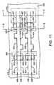
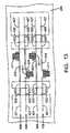
- FIGS. 11, 12 , and 14the wafer portion 200 is illustrated with gate conductor material that has been deposited and patterned.
- FIG. 11illustrates a top view of wafer portion 200
- FIG. 12illustrates a cross sectional view taken along line B—B of FIG. 11
- FIG. 14illustrates a cross sectional view taken along line C—C of FIG. 11 .
- each fin (or fin body) 406 in FIG. 11comprises portions 421 - 427 as shown. It should be noted that a transfer fin FET is formed at each location in which the gate 408 crosses over a fin 406 at fin portion 423 and 425 . Thus, FIG. 11 illustrates the formation of eight separate transfer FETs on wafer portion 200 . Additionally, a fin storage capacitor is formed at each location in which a counter electrode 410 crosses over a fin 406 at fin portion 421 and 427 . Thus, FIG.
- FIG. 11illustrates the formation of eight separate fin storage capacitors in wafer portion 200 .
- portions 421 and 427 of the fin 406embody the capacitor portion 412 shown in FIG. 10 .
- FIG. 12depicts four transfer FETs 416 on wafer portion 200 , with each transfer FET 416 having the gate 408 envelop the spacer 403 , the portion 425 of fin 406 , and the insulator layer 414 .
- FIG. 14depicts four fin storage capacitors 417 on wafer portion 200 , with each storage capacitor 417 having the counter electrode 410 envelop the spacer 403 , the portion 427 of fin 406 , and the dielectric layer 415 .
- FIGS. 12 and 14show an enlarged view of the fins such that the fin thicknesses of fin portions 425 and 427 are shown on a different geometric scale than are the corresponding fin thicknesses in FIG. 11 .
- the next step 120is to perform a sidewall reoxidation and then to form source/drain implants.
- the sidewall reoxidationagain serves to clean the sides of the fin that may have been damaged during the patterning of the gate structure.
- the source/drain implantsare preferably done by performing an angled implant into the sidewall of the fin to form the source and drain regions.
- the angled implantspreferably comprise arsenic for n-type FETs or boron difluoride for p-type FETs, tilted between 45 degrees and 75 degrees from a ray normal to the plane of the wafer.
- the doses and energies of the these implantspreferably range from between 2 ⁇ 10 14 to 1 ⁇ 10 15 cm ⁇ 2 at 0.5 to 5 keV.
- the next step 122is to form contacts and complete the memory cells.
- the contacts formedwould typically include bit line contacts and wordline contacts. Additionally, it would also include the formation of contacts to the counter electrodes of the capacitor, allowing the counter electrode to be tied to a potential such as ground or VDD. All of these contacts can be formed using any suitable technique, such as a damascene process where an insulator is deposited, patterned to open vias, and then the vias are filled with a suitable conductive material.
- bit line contactwould be formed across each fin.
- FIG. 13the wafer portion 200 is illustrated after the bit line contact 411 has been formed within portion 424 across each fin 406 .
- the devicescan be completed using any suitable back end of line processing and packaging as desired.
- the present inventionprovides a memory cell and method for forming the same that results in improved cell density without overly increasing fabrication cost and complexity.
- the preferred embodiment of the present inventionprovides a fin design to form the memory cell. Specifically, a fin Field Effect Transistor (FET) is formed to provide the access transistor, and a fin capacitor is formed to provide the storage capacitor.
- FETfin Field Effect Transistor
- the memory cell densitycan be greatly increased over traditional planar capacitor designs. Additionally, the memory cell can be formed with significantly less process cost and complexity than traditional deep trench capacitor designs.
Landscapes
- Engineering & Computer Science (AREA)
- Manufacturing & Machinery (AREA)
- Semiconductor Memories (AREA)
- Thin Film Transistor (AREA)
Abstract
Description
Claims (20)
Priority Applications (3)
| Application Number | Priority Date | Filing Date | Title |
|---|---|---|---|
| US10/063,330US6664582B2 (en) | 2002-04-12 | 2002-04-12 | Fin memory cell and method of fabrication |
| TW092108116ATWI256144B (en) | 2002-04-12 | 2003-04-09 | Fin memory cell and method of fabrication |
| JP2003107565AJP2003318286A (en) | 2002-04-12 | 2003-04-11 | Fin memory cell and method of manufacturing the same |
Applications Claiming Priority (1)
| Application Number | Priority Date | Filing Date | Title |
|---|---|---|---|
| US10/063,330US6664582B2 (en) | 2002-04-12 | 2002-04-12 | Fin memory cell and method of fabrication |
Publications (2)
| Publication Number | Publication Date |
|---|---|
| US20030197194A1 US20030197194A1 (en) | 2003-10-23 |
| US6664582B2true US6664582B2 (en) | 2003-12-16 |
Family
ID=29214350
Family Applications (1)
| Application Number | Title | Priority Date | Filing Date |
|---|---|---|---|
| US10/063,330Expired - LifetimeUS6664582B2 (en) | 2002-04-12 | 2002-04-12 | Fin memory cell and method of fabrication |
Country Status (3)
| Country | Link |
|---|---|
| US (1) | US6664582B2 (en) |
| JP (1) | JP2003318286A (en) |
| TW (1) | TWI256144B (en) |
Cited By (33)
| Publication number | Priority date | Publication date | Assignee | Title |
|---|---|---|---|---|
| US6787476B1 (en)* | 2003-08-04 | 2004-09-07 | Advanced Micro Devices, Inc. | Etch stop layer for etching FinFET gate over a large topography |
| US20040251485A1 (en)* | 2003-06-11 | 2004-12-16 | Masaru Kito | Semiconductor memory device with surface strap and method of fabricating the same |
| US20050082578A1 (en)* | 2003-06-25 | 2005-04-21 | Nowak Edward J. | High-density FinFET integration scheme |
| US20050191795A1 (en)* | 2004-03-01 | 2005-09-01 | Dureseti Chidambarrao | Method of manufacture of FinFET devices with T-shaped fins and devices manufactured thereby |
| US6947275B1 (en) | 2004-10-18 | 2005-09-20 | International Business Machines Corporation | Fin capacitor |
| US20050285204A1 (en)* | 2004-06-28 | 2005-12-29 | Sungmin Kim | Semiconductor device including a multi-channel fin field effect transistor and method of fabricating the same |
| US20060084243A1 (en)* | 2004-10-20 | 2006-04-20 | Ying Zhang | Oxidation sidewall image transfer patterning method |
| US20060160302A1 (en)* | 2004-12-10 | 2006-07-20 | Kim Sung-Min | Method of fabricating a fin field effect transistor having a plurality of protruding channels |
| US20060231907A1 (en)* | 2005-04-14 | 2006-10-19 | Samsung Electronics Co., Ltd. | Semiconductor device with FinFET and method of fabricating the same |
| US20070010049A1 (en)* | 2005-06-21 | 2007-01-11 | International Business Machines Corporation | Thermal dissipation structures for finfets |
| US20070018237A1 (en)* | 2005-07-22 | 2007-01-25 | Samsung Electronics Co., Ltd. | Non-volatile memory device having fin-type channel region and method of fabricating the same |
| US20070111455A1 (en)* | 2005-11-14 | 2007-05-17 | Samsung Electronics Co., Ltd. | Fabrication of local damascene finFETs using contact type nitride damascene mask |
| US20070141781A1 (en)* | 2005-12-20 | 2007-06-21 | Samsung Electronics Co., Ltd. | Multi-bit non-volatile memory devices and methods of fabricating the same |
| US20070145431A1 (en)* | 2005-12-24 | 2007-06-28 | Samsung Electronics Co., Ltd. | Fin-FET having GAA structure and methods of fabricating the same |
| US20070181959A1 (en)* | 2006-02-07 | 2007-08-09 | Samsung Electronics Co., Ltd. | Semiconductor device having gate-all-around structure and method of fabricating the same |
| US20070222036A1 (en)* | 2006-03-24 | 2007-09-27 | Samsung Electronics Co., Ltd. | Semiconductor memory device and methods of manufacturing and operating the same |
| US20070284632A1 (en)* | 2006-06-09 | 2007-12-13 | Samsung Electronics Co., Ltd. | Non-volatile memory device and a method of fabricating the same |
| US20080017934A1 (en)* | 2006-05-18 | 2008-01-24 | Samsung Electronic Co., Ltd. | Wire-type semiconductor devices and methods of fabricating the same |
| US20080054374A1 (en)* | 2006-08-30 | 2008-03-06 | Elpida Memory, Inc. | Semiconductor device having fin field effect transistor and manufacturing method thereof |
| US20080111199A1 (en)* | 2006-11-15 | 2008-05-15 | Kim Suk-Pil | Semiconductor device having a pair of fins and method of manufacturing the same |
| US20080157176A1 (en)* | 2006-12-28 | 2008-07-03 | Kim Won-Joo | Nonvolatile memory device and method of fabricating the same |
| US20080296648A1 (en)* | 2007-05-30 | 2008-12-04 | International Business Machines Corporation | Fin memory structure and method for fabrication thereof |
| CN100461420C (en)* | 2004-06-29 | 2009-02-11 | 国际商业机器公司 | Double gate fin field effect transistor gain unit and manufacturing method thereof |
| US20090096003A1 (en)* | 2007-10-11 | 2009-04-16 | International Business Machines Corporation | Semiconductor cell structure including buried capacitor and method for fabrication thereof |
| CN1979894B (en)* | 2005-12-05 | 2011-08-03 | 旺宏电子股份有限公司 | Memory cell, method of manufacturing and operating method of memory cell |
| US8158500B2 (en) | 2010-01-27 | 2012-04-17 | International Business Machines Corporation | Field effect transistors (FETS) and methods of manufacture |
| US20120126326A1 (en)* | 2010-11-23 | 2012-05-24 | Taiwan Semiconductor Manufacturing Company, Ltd. | Device and method for forming fins in integrated circuitry |
| US8610249B2 (en) | 2012-03-30 | 2013-12-17 | International Business Machines Corporation | Non-planar capacitor and method of forming the non-planar capacitor |
| US8633076B2 (en) | 2010-11-23 | 2014-01-21 | Taiwan Semiconductor Manufacturing Company, Ltd. | Method for adjusting fin width in integrated circuitry |
| US8779490B2 (en) | 2012-07-18 | 2014-07-15 | International Business Machines Corporation | DRAM with dual level word lines |
| US20150364534A1 (en)* | 2014-06-17 | 2015-12-17 | International Business Machines Corporation | Non-planar capacitors with finely tuned capacitance values and methods of forming the non-planar capacitors |
| US9385131B2 (en) | 2012-05-31 | 2016-07-05 | Globalfoundries Inc. | Wrap-around fin for contacting a capacitor strap of a DRAM |
| US9472550B2 (en) | 2010-11-23 | 2016-10-18 | Taiwan Semiconductor Manufacturing Company, Ltd. | Adjusted fin width in integrated circuitry |
Families Citing this family (23)
| Publication number | Priority date | Publication date | Assignee | Title |
|---|---|---|---|---|
| US7335934B2 (en)* | 2003-07-22 | 2008-02-26 | Innovative Silicon S.A. | Integrated circuit device, and method of fabricating same |
| US6835618B1 (en) | 2003-08-05 | 2004-12-28 | Advanced Micro Devices, Inc. | Epitaxially grown fin for FinFET |
| JP2005277189A (en)* | 2004-03-25 | 2005-10-06 | Renesas Technology Corp | Magnetic storage device |
| JP4195409B2 (en)* | 2004-04-09 | 2008-12-10 | 株式会社東芝 | Semiconductor memory device |
| KR100629388B1 (en)* | 2004-07-02 | 2006-09-29 | 삼성전자주식회사 | Semiconductor storage devices employing cell switching transistors having multiple channel regions and methods of manufacturing the same |
| US7482616B2 (en) | 2004-05-27 | 2009-01-27 | Samsung Electronics Co., Ltd. | Semiconductor devices having phase change memory cells, electronic systems employing the same and methods of fabricating the same |
| US7771604B2 (en)* | 2004-10-04 | 2010-08-10 | International Business Machines Corporation | Reduced mask count gate conductor definition |
| US7196380B2 (en)* | 2005-01-13 | 2007-03-27 | International Business Machines Corporation | High mobility plane FinFET with equal drive strength |
| US7348642B2 (en) | 2005-08-03 | 2008-03-25 | International Business Machines Corporation | Fin-type field effect transistor |
| US7323374B2 (en)* | 2005-09-19 | 2008-01-29 | International Business Machines Corporation | Dense chevron finFET and method of manufacturing same |
| US7265013B2 (en)* | 2005-09-19 | 2007-09-04 | International Business Machines Corporation | Sidewall image transfer (SIT) technologies |
| US20070117311A1 (en)* | 2005-11-23 | 2007-05-24 | Advanced Technology Development Facility, Inc. | Three-dimensional single transistor semiconductor memory device and methods for making same |
| US7264743B2 (en)* | 2006-01-23 | 2007-09-04 | Lam Research Corporation | Fin structure formation |
| US8217435B2 (en) | 2006-12-22 | 2012-07-10 | Intel Corporation | Floating body memory cell having gates favoring different conductivity type regions |
| US20080237678A1 (en)* | 2007-03-27 | 2008-10-02 | Suman Datta | On-chip memory cell and method of manufacturing same |
| US8420476B2 (en)* | 2010-05-27 | 2013-04-16 | International Business Machines Corporation | Integrated circuit with finFETs and MIM fin capacitor |
| JP5571030B2 (en)* | 2011-04-13 | 2014-08-13 | 株式会社東芝 | Integrated circuit device and manufacturing method thereof |
| US9318431B2 (en)* | 2011-11-04 | 2016-04-19 | Taiwan Semiconductor Manufacturing Company, Ltd. | Integrated circuit having a MOM capacitor and method of making same |
| JP5524167B2 (en)* | 2011-12-05 | 2014-06-18 | 株式会社東芝 | Manufacturing method of semiconductor device |
| US8987835B2 (en)* | 2012-03-27 | 2015-03-24 | Taiwan Semiconductor Manufacturing Company, Ltd. | FinFET with a buried semiconductor material between two fins |
| US10854455B2 (en)* | 2016-11-21 | 2020-12-01 | Marvell Asia Pte, Ltd. | Methods and apparatus for fabricating IC chips with tilted patterning |
| WO2021097770A1 (en)* | 2019-11-21 | 2021-05-27 | Huawei Technologies Co., Ltd. | Imaging element, imaging sensor, camera system, and device comprising camera system |
| CN115274664B (en)* | 2021-04-30 | 2025-09-16 | 华为技术有限公司 | Three-dimensional memory, chip packaging structure and electronic equipment |
Citations (12)
| Publication number | Priority date | Publication date | Assignee | Title |
|---|---|---|---|---|
| US5266512A (en)* | 1991-10-23 | 1993-11-30 | Motorola, Inc. | Method for forming a nested surface capacitor |
| US5323038A (en)* | 1992-04-16 | 1994-06-21 | Micron Technology, Inc. | Array of finned memory cell capacitors on a semiconductor substrate |
| US5460999A (en)* | 1994-06-06 | 1995-10-24 | United Microelectronics Corporation | Method for making fin-shaped stack capacitors on DRAM chips |
| US5497019A (en) | 1994-09-22 | 1996-03-05 | The Aerospace Corporation | Silicon-on-insulator gate-all-around MOSFET devices and fabrication methods |
| US5502332A (en)* | 1991-09-19 | 1996-03-26 | Fujitsu Limited | Semiconductor device having a belt cover film |
| US5666311A (en) | 1993-02-26 | 1997-09-09 | Kabushiki Kaisha Toshiba | Method of making semiconductor device having isolating trenches |
| US5858841A (en) | 1997-01-20 | 1999-01-12 | United Microelectronics Corporation | ROM device having memory units arranged in three dimensions, and a method of making the same |
| US6064085A (en)* | 1998-06-03 | 2000-05-16 | Texas Instruments-Acer Incorporated | DRAM cell with a multiple fin-shaped structure capacitor |
| US6064090A (en) | 1996-01-17 | 2000-05-16 | Mitsubishi Denki Kabushiki Kaisha | Semiconductor device having a portion of gate electrode formed on an insulating substrate |
| US6078493A (en)* | 1994-12-15 | 2000-06-20 | Samsung Electronics Co., Ltd. | Fin-shaped capacitor |
| US6121651A (en) | 1998-07-30 | 2000-09-19 | International Business Machines Corporation | Dram cell with three-sided-gate transfer device |
| US6261886B1 (en) | 1998-08-04 | 2001-07-17 | Texas Instruments Incorporated | Increased gate to body coupling and application to DRAM and dynamic circuits |
- 2002
- 2002-04-12USUS10/063,330patent/US6664582B2/ennot_activeExpired - Lifetime
- 2003
- 2003-04-09TWTW092108116Apatent/TWI256144B/ennot_activeIP Right Cessation
- 2003-04-11JPJP2003107565Apatent/JP2003318286A/enactivePending
Patent Citations (12)
| Publication number | Priority date | Publication date | Assignee | Title |
|---|---|---|---|---|
| US5502332A (en)* | 1991-09-19 | 1996-03-26 | Fujitsu Limited | Semiconductor device having a belt cover film |
| US5266512A (en)* | 1991-10-23 | 1993-11-30 | Motorola, Inc. | Method for forming a nested surface capacitor |
| US5323038A (en)* | 1992-04-16 | 1994-06-21 | Micron Technology, Inc. | Array of finned memory cell capacitors on a semiconductor substrate |
| US5666311A (en) | 1993-02-26 | 1997-09-09 | Kabushiki Kaisha Toshiba | Method of making semiconductor device having isolating trenches |
| US5460999A (en)* | 1994-06-06 | 1995-10-24 | United Microelectronics Corporation | Method for making fin-shaped stack capacitors on DRAM chips |
| US5497019A (en) | 1994-09-22 | 1996-03-05 | The Aerospace Corporation | Silicon-on-insulator gate-all-around MOSFET devices and fabrication methods |
| US6078493A (en)* | 1994-12-15 | 2000-06-20 | Samsung Electronics Co., Ltd. | Fin-shaped capacitor |
| US6064090A (en) | 1996-01-17 | 2000-05-16 | Mitsubishi Denki Kabushiki Kaisha | Semiconductor device having a portion of gate electrode formed on an insulating substrate |
| US5858841A (en) | 1997-01-20 | 1999-01-12 | United Microelectronics Corporation | ROM device having memory units arranged in three dimensions, and a method of making the same |
| US6064085A (en)* | 1998-06-03 | 2000-05-16 | Texas Instruments-Acer Incorporated | DRAM cell with a multiple fin-shaped structure capacitor |
| US6121651A (en) | 1998-07-30 | 2000-09-19 | International Business Machines Corporation | Dram cell with three-sided-gate transfer device |
| US6261886B1 (en) | 1998-08-04 | 2001-07-17 | Texas Instruments Incorporated | Increased gate to body coupling and application to DRAM and dynamic circuits |
Non-Patent Citations (2)
| Title |
|---|
| "1G DRAM cell with diagonal bit-line (DBL) confifuration and edge MOS (ESO) FET", Shibahara, et al., Electron Devices Meeting, 1994, Technical Digest, International, 1994, pp. 639-642. |
| "Effects a new trench-isolated transistor using sidewall gates", Hieda, et al., Hamamoto Electron Devices, IEEE Transaction on, vol. 36, Issue 9, Part 2, Sep. 1989, 1615-1619. |
Cited By (68)
| Publication number | Priority date | Publication date | Assignee | Title |
|---|---|---|---|---|
| US20050127420A1 (en)* | 2003-04-25 | 2005-06-16 | Kabushiki Kaisha Toshiba | Semiconductor memory device with surface strap and method of fabricating the same |
| US7135368B2 (en) | 2003-04-25 | 2006-11-14 | Kabushiki Kaisha Toshiba | Semiconductor memory device with surface strap and method of fabricating the same |
| US20040251485A1 (en)* | 2003-06-11 | 2004-12-16 | Masaru Kito | Semiconductor memory device with surface strap and method of fabricating the same |
| US6867450B2 (en)* | 2003-06-11 | 2005-03-15 | Kabushiki Kaisha Toshiba | Semiconductor memory device with surface strap and method of fabricating the same |
| US6987289B2 (en)* | 2003-06-25 | 2006-01-17 | International Business Machines Corporation | High-density FinFET integration scheme |
| US20050082578A1 (en)* | 2003-06-25 | 2005-04-21 | Nowak Edward J. | High-density FinFET integration scheme |
| US6787476B1 (en)* | 2003-08-04 | 2004-09-07 | Advanced Micro Devices, Inc. | Etch stop layer for etching FinFET gate over a large topography |
| US7060539B2 (en) | 2004-03-01 | 2006-06-13 | International Business Machines Corporation | Method of manufacture of FinFET devices with T-shaped fins and devices manufactured thereby |
| US20050191795A1 (en)* | 2004-03-01 | 2005-09-01 | Dureseti Chidambarrao | Method of manufacture of FinFET devices with T-shaped fins and devices manufactured thereby |
| US7394116B2 (en) | 2004-06-28 | 2008-07-01 | Samsung Electronics Co., Ltd. | Semiconductor device including a multi-channel fin field effect transistor including protruding active portions and method of fabricating the same |
| US20050285204A1 (en)* | 2004-06-28 | 2005-12-29 | Sungmin Kim | Semiconductor device including a multi-channel fin field effect transistor and method of fabricating the same |
| CN100461420C (en)* | 2004-06-29 | 2009-02-11 | 国际商业机器公司 | Double gate fin field effect transistor gain unit and manufacturing method thereof |
| US6947275B1 (en) | 2004-10-18 | 2005-09-20 | International Business Machines Corporation | Fin capacitor |
| US20060084243A1 (en)* | 2004-10-20 | 2006-04-20 | Ying Zhang | Oxidation sidewall image transfer patterning method |
| US20060160302A1 (en)* | 2004-12-10 | 2006-07-20 | Kim Sung-Min | Method of fabricating a fin field effect transistor having a plurality of protruding channels |
| US7285456B2 (en) | 2004-12-10 | 2007-10-23 | Samsung Electronics Co., Ltd. | Method of fabricating a fin field effect transistor having a plurality of protruding channels |
| US20060231907A1 (en)* | 2005-04-14 | 2006-10-19 | Samsung Electronics Co., Ltd. | Semiconductor device with FinFET and method of fabricating the same |
| US20090239346A1 (en)* | 2005-04-14 | 2009-09-24 | Samsung Electronics Co., Ltd. | Semiconductor device with finfet and method of fabricating the same |
| US7972914B2 (en) | 2005-04-14 | 2011-07-05 | Samsung Electronics Co., Ltd. | Semiconductor device with FinFET and method of fabricating the same |
| US20070010049A1 (en)* | 2005-06-21 | 2007-01-11 | International Business Machines Corporation | Thermal dissipation structures for finfets |
| US7268397B2 (en) | 2005-06-21 | 2007-09-11 | International Business Machines Corporation | Thermal dissipation structures for finfets |
| US20070224743A1 (en)* | 2005-06-21 | 2007-09-27 | Anderson Brent A | Thermal dissipation structures for finfets |
| US7387937B2 (en) | 2005-06-21 | 2008-06-17 | International Business Machines Corporation | Thermal dissipation structures for FinFETs |
| US20070018237A1 (en)* | 2005-07-22 | 2007-01-25 | Samsung Electronics Co., Ltd. | Non-volatile memory device having fin-type channel region and method of fabricating the same |
| US7902607B2 (en) | 2005-11-14 | 2011-03-08 | Samsung Electronics Co., Ltd. | Fabrication of local damascene finFETs using contact type nitride damascene mask |
| US20070111455A1 (en)* | 2005-11-14 | 2007-05-17 | Samsung Electronics Co., Ltd. | Fabrication of local damascene finFETs using contact type nitride damascene mask |
| US20090121292A1 (en)* | 2005-11-14 | 2009-05-14 | Yong-Sung Kim | Fabrication of local damascene finFETs using contact type nitride damascene mask |
| US7488654B2 (en) | 2005-11-14 | 2009-02-10 | Samsung Electronics Co., Ltd. | Fabrication of local damascene finFETs using contact type nitride damascene mask |
| CN1979894B (en)* | 2005-12-05 | 2011-08-03 | 旺宏电子股份有限公司 | Memory cell, method of manufacturing and operating method of memory cell |
| US20070141781A1 (en)* | 2005-12-20 | 2007-06-21 | Samsung Electronics Co., Ltd. | Multi-bit non-volatile memory devices and methods of fabricating the same |
| US7842995B2 (en) | 2005-12-20 | 2010-11-30 | Samsung Electronics Co., Ltd. | Multi-bit non-volatile memory devices and methods of fabricating the same |
| US20070145431A1 (en)* | 2005-12-24 | 2007-06-28 | Samsung Electronics Co., Ltd. | Fin-FET having GAA structure and methods of fabricating the same |
| US7514325B2 (en) | 2005-12-24 | 2009-04-07 | Samsung Electronics Co., Ltd. | Fin-FET having GAA structure and methods of fabricating the same |
| US7652308B2 (en) | 2006-02-07 | 2010-01-26 | Samsung Electronics Co., Ltd. | Semiconductor device having gate-all-around structure and method of fabricating the same |
| US20070181959A1 (en)* | 2006-02-07 | 2007-08-09 | Samsung Electronics Co., Ltd. | Semiconductor device having gate-all-around structure and method of fabricating the same |
| US20070222036A1 (en)* | 2006-03-24 | 2007-09-27 | Samsung Electronics Co., Ltd. | Semiconductor memory device and methods of manufacturing and operating the same |
| US7518181B2 (en) | 2006-03-24 | 2009-04-14 | Samsung Electronics Co., Ltd. | Semiconductor memory device and methods of manufacturing and operating the same |
| US20080017934A1 (en)* | 2006-05-18 | 2008-01-24 | Samsung Electronic Co., Ltd. | Wire-type semiconductor devices and methods of fabricating the same |
| US7663166B2 (en) | 2006-05-18 | 2010-02-16 | Samsung Electronics Co., Ltd. | Wire-type semiconductor devices and methods of fabricating the same |
| US20070284632A1 (en)* | 2006-06-09 | 2007-12-13 | Samsung Electronics Co., Ltd. | Non-volatile memory device and a method of fabricating the same |
| US7622765B2 (en) | 2006-06-09 | 2009-11-24 | Samsung Electronics Co., Ltd. | Non-volatile memory device and a method of fabricating the same |
| US7683437B2 (en)* | 2006-08-30 | 2010-03-23 | Elpida Memory, Inc. | Semiconductor device having fin field effect transistor and manufacturing method thereof |
| US20080054374A1 (en)* | 2006-08-30 | 2008-03-06 | Elpida Memory, Inc. | Semiconductor device having fin field effect transistor and manufacturing method thereof |
| US7833890B2 (en) | 2006-11-15 | 2010-11-16 | Samsung Electronics Co., Ltd. | Semiconductor device having a pair of fins and method of manufacturing the same |
| US7560344B2 (en) | 2006-11-15 | 2009-07-14 | Samsung Electronics Co., Ltd. | Semiconductor device having a pair of fins and method of manufacturing the same |
| US20080111199A1 (en)* | 2006-11-15 | 2008-05-15 | Kim Suk-Pil | Semiconductor device having a pair of fins and method of manufacturing the same |
| US20090253255A1 (en)* | 2006-11-15 | 2009-10-08 | Kim Won-Joo | Semiconductor device having a pair of fins and method of manufacturing the same |
| US20080157176A1 (en)* | 2006-12-28 | 2008-07-03 | Kim Won-Joo | Nonvolatile memory device and method of fabricating the same |
| US7932551B2 (en) | 2006-12-28 | 2011-04-26 | Samsung Electronics Co., Ltd. | Nonvolatile memory device and method of fabricating the same comprising a dual fin structure |
| US7696040B2 (en) | 2007-05-30 | 2010-04-13 | International Business Machines Corporation | Method for fabrication of fin memory structure |
| US20080296648A1 (en)* | 2007-05-30 | 2008-12-04 | International Business Machines Corporation | Fin memory structure and method for fabrication thereof |
| US20090096003A1 (en)* | 2007-10-11 | 2009-04-16 | International Business Machines Corporation | Semiconductor cell structure including buried capacitor and method for fabrication thereof |
| US8445949B2 (en) | 2010-01-27 | 2013-05-21 | International Business Machines Corporation | Field effect transistors (FETS) and methods of manufacture |
| US8158500B2 (en) | 2010-01-27 | 2012-04-17 | International Business Machines Corporation | Field effect transistors (FETS) and methods of manufacture |
| US8946801B2 (en) | 2010-01-27 | 2015-02-03 | International Business Machines Corporation | Field effect transistors (FETs) and methods of manufacture |
| CN102479809A (en)* | 2010-11-23 | 2012-05-30 | 台湾积体电路制造股份有限公司 | Device and method for forming fins in integrated circuitry |
| US8525267B2 (en)* | 2010-11-23 | 2013-09-03 | Taiwan Semiconductor Manufacturing Company, Ltd. | Device and method for forming Fins in integrated circuitry |
| US8633076B2 (en) | 2010-11-23 | 2014-01-21 | Taiwan Semiconductor Manufacturing Company, Ltd. | Method for adjusting fin width in integrated circuitry |
| US20120126326A1 (en)* | 2010-11-23 | 2012-05-24 | Taiwan Semiconductor Manufacturing Company, Ltd. | Device and method for forming fins in integrated circuitry |
| US9472550B2 (en) | 2010-11-23 | 2016-10-18 | Taiwan Semiconductor Manufacturing Company, Ltd. | Adjusted fin width in integrated circuitry |
| CN102479809B (en)* | 2010-11-23 | 2017-03-01 | 台湾积体电路制造股份有限公司 | For forming the Apparatus and method for of fin in integrated circuits |
| US8610249B2 (en) | 2012-03-30 | 2013-12-17 | International Business Machines Corporation | Non-planar capacitor and method of forming the non-planar capacitor |
| US9385131B2 (en) | 2012-05-31 | 2016-07-05 | Globalfoundries Inc. | Wrap-around fin for contacting a capacitor strap of a DRAM |
| US10290637B2 (en) | 2012-05-31 | 2019-05-14 | Globalfoundries Inc. | Wrap-around fin for contacting a capacitor strap of a DRAM |
| US8779490B2 (en) | 2012-07-18 | 2014-07-15 | International Business Machines Corporation | DRAM with dual level word lines |
| US9059031B2 (en) | 2012-07-18 | 2015-06-16 | International Business Machines Corporation | DRAM with dual level word lines |
| US20150364534A1 (en)* | 2014-06-17 | 2015-12-17 | International Business Machines Corporation | Non-planar capacitors with finely tuned capacitance values and methods of forming the non-planar capacitors |
| US9373678B2 (en)* | 2014-06-17 | 2016-06-21 | Globalfoundries Inc. | Non-planar capacitors with finely tuned capacitance values and methods of forming the non-planar capacitors |
Also Published As
| Publication number | Publication date |
|---|---|
| TW200403864A (en) | 2004-03-01 |
| TWI256144B (en) | 2006-06-01 |
| US20030197194A1 (en) | 2003-10-23 |
| JP2003318286A (en) | 2003-11-07 |
Similar Documents
| Publication | Publication Date | Title |
|---|---|---|
| US6664582B2 (en) | Fin memory cell and method of fabrication | |
| US6967351B2 (en) | Finfet SRAM cell using low mobility plane for cell stability and method for forming | |
| KR101464886B1 (en) | Cell layout for sram finfet transistors | |
| US7052958B1 (en) | FinFET CMOS with NVRAM capability | |
| US7378710B2 (en) | FinFET SRAM cell using inverted FinFET thin film transistors | |
| KR0165398B1 (en) | Vertical transistor manufacturing method | |
| US7060553B2 (en) | Formation of capacitor having a Fin structure | |
| KR100391985B1 (en) | Method of making a scalable two transistor memory device | |
| US7285467B2 (en) | Methods of fabricating static random access memories (SRAMS) having vertical transistors | |
| US7101741B2 (en) | Dual double gate transistor and method for forming | |
| US7915691B2 (en) | High density SRAM cell with hybrid devices | |
| US20120202330A1 (en) | Semiconductor device and method of manufacturing the same | |
| US5470776A (en) | Method for fabricating stacked dynamic random access memory cell | |
| JP2004505466A (en) | Semiconductor memory cell structure and method of manufacturing the same | |
| JPH0653435A (en) | Integrated circuit cell | |
| US7323379B2 (en) | Fabrication process for increased capacitance in an embedded DRAM memory | |
| US7563669B2 (en) | Integrated circuit with a trench capacitor structure and method of manufacture | |
| KR100423765B1 (en) | Integrated circuit comprising vertical transistors, and a method for the production thereof | |
| EP1586108A1 (en) | Finfet sram cell using inverted finfet thin film transistors | |
| US20060022302A1 (en) | Integrated circuit arrangement comprising capacitors and preferably planar transistors, and production method | |
| US7312110B2 (en) | Methods of fabricating semiconductor devices having thin film transistors | |
| US5236858A (en) | Method of manufacturing a semiconductor device with vertically stacked structure | |
| KR100226780B1 (en) | Dram cell manufacturing method | |
| US20070232002A1 (en) | Static random access memory using independent double gate transistors | |
| CN112563205A (en) | Method for forming semiconductor device |
Legal Events
| Date | Code | Title | Description |
|---|---|---|---|
| AS | Assignment | Owner name:INTERNATIONAL BUSINESS MACHINES CORPORATION, NEW Y Free format text:ASSIGNMENT OF ASSIGNORS INTEREST;ASSIGNORS:FRIED, DAVID M.;NOWAK, EDWARD J.;RAINEY, BETH ANN;REEL/FRAME:012589/0069;SIGNING DATES FROM 20020409 TO 20020410 | |
| STCF | Information on status: patent grant | Free format text:PATENTED CASE | |
| FEPP | Fee payment procedure | Free format text:PAYOR NUMBER ASSIGNED (ORIGINAL EVENT CODE: ASPN); ENTITY STATUS OF PATENT OWNER: LARGE ENTITY | |
| FPAY | Fee payment | Year of fee payment:4 | |
| FPAY | Fee payment | Year of fee payment:8 | |
| FPAY | Fee payment | Year of fee payment:12 | |
| AS | Assignment | Owner name:GLOBALFOUNDRIES U.S. 2 LLC, NEW YORK Free format text:ASSIGNMENT OF ASSIGNORS INTEREST;ASSIGNOR:INTERNATIONAL BUSINESS MACHINES CORPORATION;REEL/FRAME:036550/0001 Effective date:20150629 | |
| AS | Assignment | Owner name:GLOBALFOUNDRIES INC., CAYMAN ISLANDS Free format text:ASSIGNMENT OF ASSIGNORS INTEREST;ASSIGNORS:GLOBALFOUNDRIES U.S. 2 LLC;GLOBALFOUNDRIES U.S. INC.;REEL/FRAME:036779/0001 Effective date:20150910 | |
| AS | Assignment | Owner name:WILMINGTON TRUST, NATIONAL ASSOCIATION, DELAWARE Free format text:SECURITY AGREEMENT;ASSIGNOR:GLOBALFOUNDRIES INC.;REEL/FRAME:049490/0001 Effective date:20181127 | |
| AS | Assignment | Owner name:GLOBALFOUNDRIES U.S. INC., CALIFORNIA Free format text:ASSIGNMENT OF ASSIGNORS INTEREST;ASSIGNOR:GLOBALFOUNDRIES INC.;REEL/FRAME:054633/0001 Effective date:20201022 | |
| AS | Assignment | Owner name:GLOBALFOUNDRIES INC., CAYMAN ISLANDS Free format text:RELEASE BY SECURED PARTY;ASSIGNOR:WILMINGTON TRUST, NATIONAL ASSOCIATION;REEL/FRAME:054636/0001 Effective date:20201117 | |
| AS | Assignment | Owner name:GLOBALFOUNDRIES U.S. INC., NEW YORK Free format text:RELEASE BY SECURED PARTY;ASSIGNOR:WILMINGTON TRUST, NATIONAL ASSOCIATION;REEL/FRAME:056987/0001 Effective date:20201117 |