US6664187B1 - Laser thermal annealing for Cu seedlayer enhancement - Google Patents
Laser thermal annealing for Cu seedlayer enhancementDownload PDFInfo
- Publication number
- US6664187B1 US6664187B1US10/114,462US11446202AUS6664187B1US 6664187 B1US6664187 B1US 6664187B1US 11446202 AUS11446202 AUS 11446202AUS 6664187 B1US6664187 B1US 6664187B1
- Authority
- US
- United States
- Prior art keywords
- seedlayer
- enhancement film
- depositing
- opening
- thermal annealing
- Prior art date
- Legal status (The legal status is an assumption and is not a legal conclusion. Google has not performed a legal analysis and makes no representation as to the accuracy of the status listed.)
- Expired - Lifetime
Links
- 238000000137annealingMethods0.000titleclaimsabstractdescription26
- 238000000034methodMethods0.000claimsabstractdescription37
- 238000000151depositionMethods0.000claimsabstractdescription33
- 239000004065semiconductorSubstances0.000claimsabstractdescription20
- IJGRMHOSHXDMSA-UHFFFAOYSA-NAtomic nitrogenChemical compoundN#NIJGRMHOSHXDMSA-UHFFFAOYSA-N0.000claimsabstractdescription14
- 230000009977dual effectEffects0.000claimsabstractdescription11
- 229910052757nitrogenInorganic materials0.000claimsabstractdescription7
- 239000010949copperSubstances0.000claimsdescription55
- 229910000881Cu alloyInorganic materials0.000claimsdescription20
- 230000004888barrier functionEffects0.000claimsdescription18
- 229910052802copperInorganic materials0.000claimsdescription18
- 239000003989dielectric materialSubstances0.000claimsdescription17
- 230000008021depositionEffects0.000claimsdescription11
- 238000004519manufacturing processMethods0.000claimsdescription10
- 238000005240physical vapour depositionMethods0.000claimsdescription10
- KDLHZDBZIXYQEI-UHFFFAOYSA-NPalladiumChemical compound[Pd]KDLHZDBZIXYQEI-UHFFFAOYSA-N0.000claimsdescription8
- 238000004891communicationMethods0.000claimsdescription8
- 239000002131composite materialSubstances0.000claimsdescription8
- 238000005229chemical vapour depositionMethods0.000claimsdescription7
- 229910052715tantalumInorganic materials0.000claimsdescription7
- RYGMFSIKBFXOCR-UHFFFAOYSA-NCopperChemical compound[Cu]RYGMFSIKBFXOCR-UHFFFAOYSA-N0.000claimsdescription6
- FYYHWMGAXLPEAU-UHFFFAOYSA-NMagnesiumChemical compound[Mg]FYYHWMGAXLPEAU-UHFFFAOYSA-N0.000claimsdescription6
- 229910052749magnesiumInorganic materials0.000claimsdescription6
- 239000011777magnesiumSubstances0.000claimsdescription6
- MZLGASXMSKOWSE-UHFFFAOYSA-Ntantalum nitrideChemical compound[Ta]#NMZLGASXMSKOWSE-UHFFFAOYSA-N0.000claimsdescription6
- 239000011135tinSubstances0.000claimsdescription6
- 229910052718tinInorganic materials0.000claimsdescription6
- ATJFFYVFTNAWJD-UHFFFAOYSA-NTinChemical compound[Sn]ATJFFYVFTNAWJD-UHFFFAOYSA-N0.000claimsdescription5
- HCHKCACWOHOZIP-UHFFFAOYSA-NZincChemical compound[Zn]HCHKCACWOHOZIP-UHFFFAOYSA-N0.000claimsdescription5
- QCWXUUIWCKQGHC-UHFFFAOYSA-NZirconiumChemical compound[Zr]QCWXUUIWCKQGHC-UHFFFAOYSA-N0.000claimsdescription5
- 229910052782aluminiumInorganic materials0.000claimsdescription5
- XAGFODPZIPBFFR-UHFFFAOYSA-NaluminiumChemical compound[Al]XAGFODPZIPBFFR-UHFFFAOYSA-N0.000claimsdescription5
- 229910052725zincInorganic materials0.000claimsdescription5
- 239000011701zincSubstances0.000claimsdescription5
- 229910052726zirconiumInorganic materials0.000claimsdescription5
- BQCADISMDOOEFD-UHFFFAOYSA-NSilverChemical compound[Ag]BQCADISMDOOEFD-UHFFFAOYSA-N0.000claimsdescription4
- PCHJSUWPFVWCPO-UHFFFAOYSA-NgoldChemical compound[Au]PCHJSUWPFVWCPO-UHFFFAOYSA-N0.000claimsdescription4
- 229910052737goldInorganic materials0.000claimsdescription4
- 239000010931goldSubstances0.000claimsdescription4
- 229910052763palladiumInorganic materials0.000claimsdescription4
- 229910052709silverInorganic materials0.000claimsdescription4
- 239000004332silverSubstances0.000claimsdescription4
- PXGOKWXKJXAPGV-UHFFFAOYSA-NFluorineChemical compoundFFPXGOKWXKJXAPGV-UHFFFAOYSA-N0.000claimsdescription2
- 229910052731fluorineInorganic materials0.000claimsdescription2
- 239000011737fluorineSubstances0.000claimsdescription2
- 230000003746surface roughnessEffects0.000claimsdescription2
- 238000005275alloyingMethods0.000claims3
- 239000012535impuritySubstances0.000abstractdescription8
- 230000001747exhibiting effectEffects0.000abstractdescription2
- 239000010410layerSubstances0.000description33
- VYPSYNLAJGMNEJ-UHFFFAOYSA-NSilicium dioxideChemical compoundO=[Si]=OVYPSYNLAJGMNEJ-UHFFFAOYSA-N0.000description12
- 239000000463materialSubstances0.000description10
- 239000011229interlayerSubstances0.000description9
- 229910052751metalInorganic materials0.000description8
- 239000002184metalSubstances0.000description8
- 229910052581Si3N4Inorganic materials0.000description7
- BOTDANWDWHJENH-UHFFFAOYSA-NTetraethyl orthosilicateChemical compoundCCO[Si](OCC)(OCC)OCCBOTDANWDWHJENH-UHFFFAOYSA-N0.000description7
- 230000008901benefitEffects0.000description6
- -1poly(arylene)Polymers0.000description6
- 238000001465metallisationMethods0.000description5
- 239000000377silicon dioxideSubstances0.000description5
- 239000000758substrateSubstances0.000description5
- 238000009792diffusion processMethods0.000description4
- 238000009713electroplatingMethods0.000description4
- 238000005516engineering processMethods0.000description4
- 239000001257hydrogenSubstances0.000description4
- 229910052739hydrogenInorganic materials0.000description4
- 235000012239silicon dioxideNutrition0.000description4
- HQVNEWCFYHHQES-UHFFFAOYSA-Nsilicon nitrideChemical compoundN12[Si]34N5[Si]62N3[Si]51N64HQVNEWCFYHHQES-UHFFFAOYSA-N0.000description4
- 239000010936titaniumSubstances0.000description4
- OKTJSMMVPCPJKN-UHFFFAOYSA-NCarbonChemical compound[C]OKTJSMMVPCPJKN-UHFFFAOYSA-N0.000description3
- RTAQQCXQSZGOHL-UHFFFAOYSA-NTitaniumChemical compound[Ti]RTAQQCXQSZGOHL-UHFFFAOYSA-N0.000description3
- QVGXLLKOCUKJST-UHFFFAOYSA-Natomic oxygenChemical compound[O]QVGXLLKOCUKJST-UHFFFAOYSA-N0.000description3
- 229910052799carbonInorganic materials0.000description3
- 239000004020conductorSubstances0.000description3
- 238000013461designMethods0.000description3
- 239000001301oxygenSubstances0.000description3
- 229910052760oxygenInorganic materials0.000description3
- 239000005368silicate glassSubstances0.000description3
- HBMJWWWQQXIZIP-UHFFFAOYSA-Nsilicon carbideChemical compound[Si+]#[C-]HBMJWWWQQXIZIP-UHFFFAOYSA-N0.000description3
- 229910010271silicon carbideInorganic materials0.000description3
- 239000000126substanceSubstances0.000description3
- 229910052719titaniumInorganic materials0.000description3
- UFHFLCQGNIYNRP-UHFFFAOYSA-NHydrogenChemical compound[H][H]UFHFLCQGNIYNRP-UHFFFAOYSA-N0.000description2
- PXHVJJICTQNCMI-UHFFFAOYSA-NNickelChemical compound[Ni]PXHVJJICTQNCMI-UHFFFAOYSA-N0.000description2
- 239000004642PolyimideSubstances0.000description2
- 230000015572biosynthetic processEffects0.000description2
- 230000001419dependent effectEffects0.000description2
- 230000003028elevating effectEffects0.000description2
- 238000005530etchingMethods0.000description2
- 150000002739metalsChemical class0.000description2
- 238000012986modificationMethods0.000description2
- 230000004048modificationEffects0.000description2
- 229910021421monocrystalline siliconInorganic materials0.000description2
- 229920000620organic polymerPolymers0.000description2
- BASFCYQUMIYNBI-UHFFFAOYSA-NplatinumChemical compound[Pt]BASFCYQUMIYNBI-UHFFFAOYSA-N0.000description2
- 238000005498polishingMethods0.000description2
- 229920000412polyarylenePolymers0.000description2
- 229920001721polyimidePolymers0.000description2
- 230000008569processEffects0.000description2
- 238000012545processingMethods0.000description2
- 229910052814silicon oxideInorganic materials0.000description2
- GUVRBAGPIYLISA-UHFFFAOYSA-Ntantalum atomChemical compound[Ta]GUVRBAGPIYLISA-UHFFFAOYSA-N0.000description2
- WFKWXMTUELFFGS-UHFFFAOYSA-NtungstenChemical compound[W]WFKWXMTUELFFGS-UHFFFAOYSA-N0.000description2
- 229910052721tungstenInorganic materials0.000description2
- 239000010937tungstenSubstances0.000description2
- JBRZTFJDHDCESZ-UHFFFAOYSA-NAsGaChemical compound[As]#[Ga]JBRZTFJDHDCESZ-UHFFFAOYSA-N0.000description1
- VYZAMTAEIAYCRO-UHFFFAOYSA-NChromiumChemical compound[Cr]VYZAMTAEIAYCRO-UHFFFAOYSA-N0.000description1
- 229910001218Gallium arsenideInorganic materials0.000description1
- 239000004698PolyethyleneSubstances0.000description1
- 239000004721Polyphenylene oxideSubstances0.000description1
- 239000004743PolypropyleneSubstances0.000description1
- BLRPTPMANUNPDV-UHFFFAOYSA-NSilaneChemical compound[SiH4]BLRPTPMANUNPDV-UHFFFAOYSA-N0.000description1
- XUIMIQQOPSSXEZ-UHFFFAOYSA-NSiliconChemical compound[Si]XUIMIQQOPSSXEZ-UHFFFAOYSA-N0.000description1
- NRTOMJZYCJJWKI-UHFFFAOYSA-NTitanium nitrideChemical compound[Ti]#NNRTOMJZYCJJWKI-UHFFFAOYSA-N0.000description1
- 229910008807WSiNInorganic materials0.000description1
- GDFCWFBWQUEQIJ-UHFFFAOYSA-N[B].[P]Chemical compound[B].[P]GDFCWFBWQUEQIJ-UHFFFAOYSA-N0.000description1
- UGACIEPFGXRWCH-UHFFFAOYSA-N[Si].[Ti]Chemical compound[Si].[Ti]UGACIEPFGXRWCH-UHFFFAOYSA-N0.000description1
- 230000002411adverseEffects0.000description1
- 229910045601alloyInorganic materials0.000description1
- 239000000956alloySubstances0.000description1
- 238000013459approachMethods0.000description1
- 150000004945aromatic hydrocarbonsChemical class0.000description1
- IVHJCRXBQPGLOV-UHFFFAOYSA-NazanylidynetungstenChemical compound[W]#NIVHJCRXBQPGLOV-UHFFFAOYSA-N0.000description1
- 229910052804chromiumInorganic materials0.000description1
- 239000011651chromiumSubstances0.000description1
- 230000001934delayEffects0.000description1
- 239000002019doping agentSubstances0.000description1
- 239000012776electronic materialSubstances0.000description1
- 230000002708enhancing effectEffects0.000description1
- RTZKZFJDLAIYFH-UHFFFAOYSA-NetherSubstancesCCOCCRTZKZFJDLAIYFH-UHFFFAOYSA-N0.000description1
- 150000002170ethersChemical class0.000description1
- 239000007789gasSubstances0.000description1
- 229910052732germaniumInorganic materials0.000description1
- GNPVGFCGXDBREM-UHFFFAOYSA-Ngermanium atomChemical compound[Ge]GNPVGFCGXDBREM-UHFFFAOYSA-N0.000description1
- 238000010438heat treatmentMethods0.000description1
- 150000002431hydrogenChemical class0.000description1
- 229910052738indiumInorganic materials0.000description1
- APFVFJFRJDLVQX-UHFFFAOYSA-Nindium atomChemical compound[In]APFVFJFRJDLVQX-UHFFFAOYSA-N0.000description1
- 238000005224laser annealingMethods0.000description1
- WPBNNNQJVZRUHP-UHFFFAOYSA-Lmanganese(2+);methyl n-[[2-(methoxycarbonylcarbamothioylamino)phenyl]carbamothioyl]carbamate;n-[2-(sulfidocarbothioylamino)ethyl]carbamodithioateChemical compound[Mn+2].[S-]C(=S)NCCNC([S-])=S.COC(=O)NC(=S)NC1=CC=CC=C1NC(=S)NC(=O)OCWPBNNNQJVZRUHP-UHFFFAOYSA-L0.000description1
- 229910052759nickelInorganic materials0.000description1
- 238000010943off-gassingMethods0.000description1
- 239000011368organic materialSubstances0.000description1
- 238000000623plasma-assisted chemical vapour depositionMethods0.000description1
- 229910052697platinumInorganic materials0.000description1
- 229920000052poly(p-xylylene)Polymers0.000description1
- 229920000573polyethylenePolymers0.000description1
- 229920000642polymerPolymers0.000description1
- 229920006380polyphenylene oxidePolymers0.000description1
- 229920001155polypropylenePolymers0.000description1
- 229910000077silaneInorganic materials0.000description1
- 229910052710siliconInorganic materials0.000description1
- 239000010703siliconSubstances0.000description1
- HWEYZGSCHQNNEH-UHFFFAOYSA-Nsilicon tantalumChemical compound[Si].[Ta]HWEYZGSCHQNNEH-UHFFFAOYSA-N0.000description1
- WNUPENMBHHEARK-UHFFFAOYSA-Nsilicon tungstenChemical compound[Si].[W]WNUPENMBHHEARK-UHFFFAOYSA-N0.000description1
- 229910052712strontiumInorganic materials0.000description1
- CIOAGBVUUVVLOB-UHFFFAOYSA-Nstrontium atomChemical compound[Sr]CIOAGBVUUVVLOB-UHFFFAOYSA-N0.000description1
- 230000008685targetingEffects0.000description1
- MAKDTFFYCIMFQP-UHFFFAOYSA-Ntitanium tungstenChemical compound[Ti].[W]MAKDTFFYCIMFQP-UHFFFAOYSA-N0.000description1
Images


Classifications
- H—ELECTRICITY
- H01—ELECTRIC ELEMENTS
- H01L—SEMICONDUCTOR DEVICES NOT COVERED BY CLASS H10
- H01L21/00—Processes or apparatus adapted for the manufacture or treatment of semiconductor or solid state devices or of parts thereof
- H01L21/70—Manufacture or treatment of devices consisting of a plurality of solid state components formed in or on a common substrate or of parts thereof; Manufacture of integrated circuit devices or of parts thereof
- H01L21/71—Manufacture of specific parts of devices defined in group H01L21/70
- H01L21/768—Applying interconnections to be used for carrying current between separate components within a device comprising conductors and dielectrics
- H01L21/76838—Applying interconnections to be used for carrying current between separate components within a device comprising conductors and dielectrics characterised by the formation and the after-treatment of the conductors
- H01L21/76841—Barrier, adhesion or liner layers
- H01L21/76843—Barrier, adhesion or liner layers formed in openings in a dielectric
- H—ELECTRICITY
- H01—ELECTRIC ELEMENTS
- H01L—SEMICONDUCTOR DEVICES NOT COVERED BY CLASS H10
- H01L21/00—Processes or apparatus adapted for the manufacture or treatment of semiconductor or solid state devices or of parts thereof
- H01L21/70—Manufacture or treatment of devices consisting of a plurality of solid state components formed in or on a common substrate or of parts thereof; Manufacture of integrated circuit devices or of parts thereof
- H01L21/71—Manufacture of specific parts of devices defined in group H01L21/70
- H01L21/768—Applying interconnections to be used for carrying current between separate components within a device comprising conductors and dielectrics
- H01L21/76838—Applying interconnections to be used for carrying current between separate components within a device comprising conductors and dielectrics characterised by the formation and the after-treatment of the conductors
- H01L21/76841—Barrier, adhesion or liner layers
- H01L21/76853—Barrier, adhesion or liner layers characterized by particular after-treatment steps
- H01L21/76861—Post-treatment or after-treatment not introducing additional chemical elements into the layer
- H01L21/76862—Bombardment with particles, e.g. treatment in noble gas plasmas; UV irradiation
- H—ELECTRICITY
- H01—ELECTRIC ELEMENTS
- H01L—SEMICONDUCTOR DEVICES NOT COVERED BY CLASS H10
- H01L21/00—Processes or apparatus adapted for the manufacture or treatment of semiconductor or solid state devices or of parts thereof
- H01L21/70—Manufacture or treatment of devices consisting of a plurality of solid state components formed in or on a common substrate or of parts thereof; Manufacture of integrated circuit devices or of parts thereof
- H01L21/71—Manufacture of specific parts of devices defined in group H01L21/70
- H01L21/768—Applying interconnections to be used for carrying current between separate components within a device comprising conductors and dielectrics
- H01L21/76838—Applying interconnections to be used for carrying current between separate components within a device comprising conductors and dielectrics characterised by the formation and the after-treatment of the conductors
- H01L21/76841—Barrier, adhesion or liner layers
- H01L21/76853—Barrier, adhesion or liner layers characterized by particular after-treatment steps
- H01L21/76861—Post-treatment or after-treatment not introducing additional chemical elements into the layer
- H01L21/76864—Thermal treatment
- H—ELECTRICITY
- H01—ELECTRIC ELEMENTS
- H01L—SEMICONDUCTOR DEVICES NOT COVERED BY CLASS H10
- H01L21/00—Processes or apparatus adapted for the manufacture or treatment of semiconductor or solid state devices or of parts thereof
- H01L21/70—Manufacture or treatment of devices consisting of a plurality of solid state components formed in or on a common substrate or of parts thereof; Manufacture of integrated circuit devices or of parts thereof
- H01L21/71—Manufacture of specific parts of devices defined in group H01L21/70
- H01L21/768—Applying interconnections to be used for carrying current between separate components within a device comprising conductors and dielectrics
- H01L21/76838—Applying interconnections to be used for carrying current between separate components within a device comprising conductors and dielectrics characterised by the formation and the after-treatment of the conductors
- H01L21/76841—Barrier, adhesion or liner layers
- H01L21/76868—Forming or treating discontinuous thin films, e.g. repair, enhancement or reinforcement of discontinuous thin films
- H—ELECTRICITY
- H01—ELECTRIC ELEMENTS
- H01L—SEMICONDUCTOR DEVICES NOT COVERED BY CLASS H10
- H01L21/00—Processes or apparatus adapted for the manufacture or treatment of semiconductor or solid state devices or of parts thereof
- H01L21/70—Manufacture or treatment of devices consisting of a plurality of solid state components formed in or on a common substrate or of parts thereof; Manufacture of integrated circuit devices or of parts thereof
- H01L21/71—Manufacture of specific parts of devices defined in group H01L21/70
- H01L21/768—Applying interconnections to be used for carrying current between separate components within a device comprising conductors and dielectrics
- H01L21/76838—Applying interconnections to be used for carrying current between separate components within a device comprising conductors and dielectrics characterised by the formation and the after-treatment of the conductors
- H01L21/76841—Barrier, adhesion or liner layers
- H01L21/76871—Layers specifically deposited to enhance or enable the nucleation of further layers, i.e. seed layers
- H01L21/76873—Layers specifically deposited to enhance or enable the nucleation of further layers, i.e. seed layers for electroplating
- H—ELECTRICITY
- H01—ELECTRIC ELEMENTS
- H01L—SEMICONDUCTOR DEVICES NOT COVERED BY CLASS H10
- H01L2221/00—Processes or apparatus adapted for the manufacture or treatment of semiconductor or solid state devices or of parts thereof covered by H01L21/00
- H01L2221/10—Applying interconnections to be used for carrying current between separate components within a device
- H01L2221/1068—Formation and after-treatment of conductors
- H01L2221/1073—Barrier, adhesion or liner layers
- H01L2221/1084—Layers specifically deposited to enhance or enable the nucleation of further layers, i.e. seed layers
- H01L2221/1089—Stacks of seed layers
Definitions
- the present inventionrelates to copper (Cu) and/or Cu alloy metallization in semiconductor devices, and to a method for manufacturing semiconductor devices with reliable, low resistance Cu or Cu alloy interconnects.
- the present inventionis particularly applicable to manufacturing high speed integrated circuits having submicron design features and high conductivity interconnect structures.
- Conventional semiconductor devicescomprise a semiconductor substrate, typically doped monocrystalline silicon, and a plurality of sequentially formed interlayer dielectrics and conductive patterns.
- An integrated circuitis formed containing a plurality of conductive patterns comprising conductive lines separated by interwiring spacings, and a plurality of interconnect lines, such as bus lines, bit lines, word lines and logic interconnect lines.
- the conductive patterns on different layersi.e., upper and lower layers, are electrically connected by a conductive plug filling a via hole, while a conductive plug filling a contact hole establishes electrical contact with an active region on a semiconductor substrate, such as a source/drain region.
- Conductive linesare formed in trenches which typically extend substantially horizontal with respect to the semiconductor substrate.
- Semiconductor “chips”comprising five or more levels of metallization are becoming more prevalent as device geometry's shrink to submicron levels.
- a conductive plug filling a via holeis typically formed by depositing an interlayer dielectric on a conductive layer comprising at least one conductive pattern, forming an opening through the interlayer dielectric by conventional photolithographic and etching techniques, and filling the opening with a conductive material, such as tungsten (W). Excess conductive material on the surface of the interlayer dielectric is typically removed by chemical mechanical polishing (CMP).
- CMPchemical mechanical polishing
- damasceneOne such method is known as damascene and basically involves forming an opening in the interlayer dielectric and filling the opening with a metal. Dual damascene techniques involve forming an opening comprising a lower contact or via hole section in communication with an upper trench section, which opening is filled with a conductive material, typically a metal, to simultaneously form a conductive plug in electrical contact with a conductive line.
- Cu and Cu alloyshave received considerable attention as a candidate for replacing Al in interconnect metallizations.
- Cuis relatively inexpensive, easy to process, and has a lower resistively than Al.
- Cuhas improved electrical properties vis-a-vis W, making Cu a desirable metal for use as a conductive plug as well as conductive wiring.
- An approach to forming Cu plugs and wiringcomprises the use of damascene structures employing CMP.
- Cu interconnect structuresmust be encapsulated by a diffusion barrier layer.
- Typical diffusion barrier metalsinclude tantalum (Ta), tantalum nitride (TaN), titanium nitride (TiN), titanium (Ti), titanium-tungsten (TiW), tungsten (W), tungsten nitride (WN), Ti-TiN, titanium silicon nitride (TiSiN), tungsten silicon nitride (WSiN), tantalum silicon nitride (TaSiN) and silicon nitride for encapsulating Cu.
- the use of such barrier materials to encapsulate Cuis not limited to the interface between Cu and the dielectric interlayer, but includes interfaces with other metals as well.
- discontinuities in seedlayer 12form, as illustrated by reference numeral 13 .
- Cucannot be electroplated on a discontinuous seedlayer or where no seedlayer exists. Consequently, voids are induced leading to high resistance vias and lines or opening circuits.
- An advantage of the present inventionis a method of manufacturing a semiconductor device having reliable, low resistance Cu or Cu alloy interconnects with significantly reduced voids.
- a method of manufacturing a semiconductor devicecomprising: forming an opening in a dielectric layer; depositing a barrier layer lining the opening; depositing a seedlayer for copper (Cu) or Cu alloy deposition on the barrier layer; depositing a seedlayer enhancement film by chemical vapor deposition on the seedlayer; laser thermal annealing the seedlayer enhancement film; and filling the opening with Cu or a Cu alloy.
- Embodimentsinclude forming a dual damascene opening in dielectric material having a dielectric constant no greater than about 3.9, such as a fluorine (F)-containing oxides, such as an F-containing oxide derived from tetraethyl orthosilicate (TEOS), the opening comprising an upper trench section in communication with a lower via hole section; depositing a composite barrier layer lining the opening, the composite barrier layer comprising a layer of tantalum nitride and a layer of ⁇ -tantalum thereon; depositing a seedlayer by PVD on the ⁇ -tantalum layer, the deposited seedlayer having discontinuities, depositing a conformal seedlayer enhancement film by chemical vapor deposition bridging discontinuities in the seedlayer and having a rough surface; laser thermal annealing the seedlayer enhancement film in flowing nitrogen to reduce the roughness of the seedlayer enhancement film; and filling the opening with Cu or a Cu alloy to form a Cu or Cu alloy line in communication with an underlying Cu or Cu alloy via.
- Embodiments of the present inventioninclude laser thermal annealing by impinging a pulsed laser light beam on the rough exterior surface of the deposited seedlayer enhancement film at a radiant fluence of about 0.084 to about 0.136 joules/cm 2 for about 10 to about 100 nanoseconds, thereby elevating the temperature of the seedlayer enhancement film to about 300° C. to about 500° C.
- FIG. 1schematically illustrates a discontinuous seedlayer of problem solved by the present invention.
- FIGS. 2 through 5schematically illustrate sequential phases of a method in accordance with an embodiment of the present invention.
- FIGS. 6 through 11schematically illustrate sequential phases of a method in accordance with another embodiment of the present invention.
- the present inventionaddresses and solves various problems attendant upon forming metallized interconnects, such as Cu or Cu alloy interconnects, particularly, damascene structures in dielectric layer(s) having a dielectric constant less than about 3.9, such as F-containing dielectric material, e.g., F-containing silicon oxide derived from TEOS(F-TEOS).
- F-containing dielectric materiale.g., F-containing silicon oxide derived from TEOS(F-TEOS).
- F-containing dielectric materiale.g., F-containing silicon oxide derived from TEOS(F-TEOS).
- the symbol Cuis intended to encompass high purity elemental copper as well as Cu-based alloys, such as Cu alloys containing minor amounts of tantalum, indium, tin, zinc, manganese, titanium, magnesium, chromium, titanium, germanium, strontium, platinum, magnesium, aluminum or zirconium.
- a seedlayer enhancement filmwas deposited, using a seedlayer for Cu deposition, by chemical vapor deposition (CVD).
- CVDchemical vapor deposition
- Such a seedlayer enhancement filmis schematically illustrated in FIG. 2 by reference numeral 20 .
- the subsequently deposited electroplated Cu filmexhibits high resistivity, high surface roughness, voids and a small grain size, leading to significantly increased via/line resistance and lower circuit speed, in addition to generating electromigration and other reliability issues.
- the inadequacies of the seedlayer and seedlayer enhancement filmare addressed by strategically treating the exposed rough surface of seedlayer enhancement film by laser thermal annealing to improve its properties for subsequent Cu electroplating.
- the rough surface of the conformal seedlayer enhancement filmis subjected to a pulsed laser light beam in nitrogen, such as at a flow rate of about 200 to 2,000 sccm, for a period of time of about 10 to about 100 nanoseconds.
- the temperature of the seedlayer enhancement filmis elevated to a temperature of about 300° C. to about 500° C.
- Such laser thermal annealingimproves the quality of the seedlayer enhancement film by driving out impurities, enhancing film conductivity, reducing film stress, densifying the film and significantly reducing film roughness.
- the removal of impurities during laser thermal annealingadvantageously prevents subsequent out-gassing and, hence, reduces voiding.
- An additional benefit of laser thermal annealingcomprises thinning the seedlayer enhancement film at the bottom portion of the via and reduced overhang of the conformal seedlayer enhancement film, thereby insuring complete filling of openings with reduced voiding.
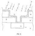
- the seedlayer enhancement film 20is subjected to laser thermal annealing, as schematically illustrated by arrows 30 , in nitrogen flowing at about rate of 200 to about 2,000 sccm.
- Laser thermal annealingalters the seedlayer enhancement film 20 , resulting in the modified seedlayer enhancement film 40 illustrated in FIG. 4 .
- the improved seedlayer enhancement film 40exhibits a smooth surface and is thinned somewhat at the bottom and comers, thereby reducing contact resistance and improving filling.
- Laser thermal annealingreduces or drives out impurities, such as carbon, oxygen and hydrogen, thereby preventing subsequent voiding in the deposited Cu.
- Subsequent processingincludes electroplating copper 50 to fill the opening as shown in FIG. 5, chemical mechanical polishing (CMP) to reduce any overburden on the upper surface of dielectric layer 10 and depositing capping layer 51 , such as silicon nitride or silicon carbide.
- CMPchemical mechanical polishing
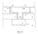
- FIGS. 6 through 11Another embodiment of the present invention is schematically illustrated in FIGS. 6 through 11, wherein similar features are denoted by similar reference numerals.
- a lower metal feature 61such as a Cu line
- a barrier layer 62encapsulating metal feature 61 .
- Dielectric layers 63 and 67are deposited with a middle etch stop layer 66 therebetween.
- Dielectric layers 63 and 67can comprise any of various dielectric materials conventionally employed and fabricating semiconductor devices, particularly low-k dielectric materials having a dielectric constant (k) no greater than about 3.9, such as F-TEOS.
- Middle etch stop layer 66can comprise silicon nitride, silicon oxynitride or silicon carbide.
- a dual damascene opening 64is then formed comprising upper trench 64 A and lower via hole section 64 B.
- Dual damascene opening 64can be formed in a conventional manner, as by a conventional via first-trench last technique or a conventional trench first-via last technique.
- a barrier layer 65is then deposited, such as a composite barrier layer comprising an initial layer of tantalum nitride and a layer of ⁇ -tantalum thereon.
- Composite barrier layer 65can be formed at a combined thickness of about 50 ⁇ to about 300 ⁇ , as by physical vapor deposition (PVD) techniques, such as ionized physical vapor deposition (IPVD), e.g., ionized sputtered deposition (ISD).
- PVDphysical vapor deposition
- IPVDionized physical vapor deposition
- ISDionized sputtered deposition
- seedlayer 70is deposited by PVD.
- Seedlayer 70is typically discontinuously formed, as illustrated by islands 70 and the absence of any seedlayer at the bottom of via hole section 64 B.
- Seedlayer 70may be formed at a thickness of about 200 ⁇ to about 300 ⁇ and may comprise a conventional seedlayer material for Cu deposition, such as Cu itself or a Cu alloy containing magnesium, aluminum, zinc, zirconium, tin, nickel, palladium, silver or gold in a suitable amount, e.g., about 0.3 to about 12 at. %.
- a seedlayer enhancement film 80is deposited by CVD, typically at a thickness of about 300 ⁇ to about 400 ⁇ . Seedlayer enhancement film 80 is conformal and typically exhibits a rough surface and contains impurities which would out-gas subsequent Cu deposition causing undesirable voids and increased resistance.
- CVDchemical vapor deposition
- the seedlayer enhancement film 80is subjected to laser thermal annealing, as schematically illustrated by arrows 90 , by impinging a pulsed laser light beam on the exposed rough surface of seedlayer enhancement film 80 , as at a radiance fluence of about 0.084 to about 0.136 joules/cm 2 , for about 10 to about 100 nanoseconds, thereby elevating the temperature of the seedlayer enhancement film 80 to about 300° C. to about 500° C.
- impurities, such as carbon, oxygen and hydrogen in the seedlayer enhancement film 80are driven out and the surface of seedlayer enhancement film 80 significantly reduced in roughness.
- Laser thermal annealingalso reduces film stress and increases the density of the film.
- the resulting structureis schematically illustrated in FIG. 10 having improved seedlayer enhancement film 100 with a smooth surface.
- Cuis deposited, as by electroplating, to form dual damascene structure comprising upper Cu line 100 B in communication with lower Cu via 110 A.
- CMPis then conducted to remove any overburden and a capping layer 111 is deposited, such as silicon nitride or silicon carbide.
- the present inventionadvantageously enables fabricating semiconductor devices having submicron features with highly reliable Cu interconnects exhibiting significantly reduced voiding and reduced contact resistance. Problems attendant upon inadequate seedlayer deposition and poor seedlayer enhancement film formation are addressed and solved by implementing laser thermal annealing to smooth the roughen surface of the seedlayer enhancement film and drive out impurities, thereby enabling filling of the opening, particularly a dual damascene opening formed in low dielectric constant materials, with improved reliability reduced voiding and reduced contact resistance.
- any of various conventional laser systemscan be employed, such as an excimer or Nd-YAG pulse laser.
- Commercially available laser tools for laser annealing, either with or without a mask,are available, such the Verdant Technologies laser anneal tool operating at an exposure wavelength of 308 nm.
- Available laser sourcesare capable of operating at energies of from about 10 to about 2,000 mj/cm 2 /pulse. Suitable operating conditions can be determined in a particular situation.
- the substratecan be doped monocrystalline silicon or gallium-arsenide.
- the interlayer dielectric employed in the present inventioncan comprise any dielectric material conventionally employed in the manufacture of semiconductor devices.
- dielectric materialssuch as silicon dioxide, phosphorous-doped silicate-glass (PSG), boron-and phosphorus doped silicate glass (BPSG), and silicon dioxide derived from tetraethylorthosilicate (TEOS) or silane by PECVD can be employed.
- the openings formed in dielectric layersare effected by conventional photolithographic and etching techniques.
- dielectric materials for use as interlayer dielectrics in accordance with embodiments of the present inventioncan comprise dielectric materials with lower values of permitivity and those mentioned above, in order to reduce interconnect capacitance.
- low-k materialhas evolved characterized materials with a dielectric constant less than about 3.9, e.g., about 3.5 or less.
- the value of a dielectric constant expressed hereinis based upon the value of (1) for a vacuum.
- low-k materialscan be employed in accordance with embodiments of the present invention, both organic and inorganic.
- Suitable organic materialsinclude various polyimides and BCB.
- Other suitable low-k dielectricsinclude poly(arylene)ethers, poly(arylene)ether azoles, parylene-N, polyimides, polynapthalene-N, polyphenylquinoxalines (PPQ), polyphenyleneoxide, polyethylene and polypropylene.
- low-k materials suitable for use in embodiments of the present inventioninclude FO x TM (HSQ-based), XLKTM (HSQ-based), and porous SILKTM, an aromatic hydrocarbon polymer (each available from Dow Chemical Co., Midland, Mich.); CoralTM, a carbon-doped silicon oxide (available from Novellus Systems, San Jose, Calif.), silicon-carbon-oxygen-hydrogen (SiCOH) organic dielectrics, Black-DiamondTM dielectrics, FlareTM, an organic polymer, HOSPTM, a hybrid sioloxane-organic polymer, and NanoglassTM, a nanoporous silica (each available from Honeywell Electronic Materials) and halogen-doped (e.g., fluorine-doped) silicon dioxide derived from tetraethyl orthosilicate (TEOS) and fluorine-doped silicate glass (FSG).
- FO x TMHSQ-based
- XLKTMHSQ-based
- the present inventionenjoys industrial applicability in fabricating various types of semiconductor devices comprising interconnects, particularly inlaid Cu metallization interconnection patterns.
- the present inventionenjoys particularly industrial applicability in fabricating semiconductor devices having submicron features and high aspect ratio openings.
Landscapes
- Engineering & Computer Science (AREA)
- Physics & Mathematics (AREA)
- Condensed Matter Physics & Semiconductors (AREA)
- General Physics & Mathematics (AREA)
- Manufacturing & Machinery (AREA)
- Computer Hardware Design (AREA)
- Microelectronics & Electronic Packaging (AREA)
- Power Engineering (AREA)
- Plasma & Fusion (AREA)
- Internal Circuitry In Semiconductor Integrated Circuit Devices (AREA)
Abstract
Description
Claims (20)
Priority Applications (1)
| Application Number | Priority Date | Filing Date | Title |
|---|---|---|---|
| US10/114,462US6664187B1 (en) | 2002-04-03 | 2002-04-03 | Laser thermal annealing for Cu seedlayer enhancement |
Applications Claiming Priority (1)
| Application Number | Priority Date | Filing Date | Title |
|---|---|---|---|
| US10/114,462US6664187B1 (en) | 2002-04-03 | 2002-04-03 | Laser thermal annealing for Cu seedlayer enhancement |
Publications (1)
| Publication Number | Publication Date |
|---|---|
| US6664187B1true US6664187B1 (en) | 2003-12-16 |
Family
ID=29709442
Family Applications (1)
| Application Number | Title | Priority Date | Filing Date |
|---|---|---|---|
| US10/114,462Expired - LifetimeUS6664187B1 (en) | 2002-04-03 | 2002-04-03 | Laser thermal annealing for Cu seedlayer enhancement |
Country Status (1)
| Country | Link |
|---|---|
| US (1) | US6664187B1 (en) |
Cited By (24)
| Publication number | Priority date | Publication date | Assignee | Title |
|---|---|---|---|---|
| US20030216040A1 (en)* | 2002-05-16 | 2003-11-20 | Lee Byung Zu | Method of forming copper wire on semiconductor device |
| US6780789B1 (en)* | 2002-08-29 | 2004-08-24 | Advanced Micro Devices, Inc. | Laser thermal oxidation to form ultra-thin gate oxide |
| US20040227243A1 (en)* | 2003-05-15 | 2004-11-18 | Dung-Ching Perng | Methods of pore sealing and metal encapsulation in porous low k interconnect |
| US7077860B2 (en) | 1997-04-24 | 2006-07-18 | Advanced Cardiovascular Systems, Inc. | Method of reducing or eliminating thrombus formation |
| US7198675B2 (en) | 2003-09-30 | 2007-04-03 | Advanced Cardiovascular Systems | Stent mandrel fixture and method for selectively coating surfaces of a stent |
| WO2007019455A3 (en)* | 2005-08-08 | 2007-06-28 | Applied Materials Inc | Copper barrier reflow process employing high speed optical annealing |
| US7258891B2 (en) | 2001-06-28 | 2007-08-21 | Advanced Cardiovascular Systems, Inc. | Stent mounting assembly and a method of using the same to coat a stent |
| US7297159B2 (en) | 2000-10-26 | 2007-11-20 | Advanced Cardiovascular Systems, Inc. | Selective coating of medical devices |
| US7312162B2 (en) | 2005-05-17 | 2007-12-25 | Applied Materials, Inc. | Low temperature plasma deposition process for carbon layer deposition |
| US7323401B2 (en) | 2005-08-08 | 2008-01-29 | Applied Materials, Inc. | Semiconductor substrate process using a low temperature deposited carbon-containing hard mask |
| US7335611B2 (en) | 2005-08-08 | 2008-02-26 | Applied Materials, Inc. | Copper conductor annealing process employing high speed optical annealing with a low temperature-deposited optical absorber layer |
| US7422775B2 (en) | 2005-05-17 | 2008-09-09 | Applied Materials, Inc. | Process for low temperature plasma deposition of an optical absorption layer and high speed optical annealing |
| US7429532B2 (en) | 2005-08-08 | 2008-09-30 | Applied Materials, Inc. | Semiconductor substrate process using an optically writable carbon-containing mask |
| US7553377B1 (en) | 2004-04-27 | 2009-06-30 | Advanced Cardiovascular Systems, Inc. | Apparatus and method for electrostatic coating of an abluminal stent surface |
| US7563324B1 (en) | 2003-12-29 | 2009-07-21 | Advanced Cardiovascular Systems Inc. | System and method for coating an implantable medical device |
| US7632307B2 (en) | 2004-12-16 | 2009-12-15 | Advanced Cardiovascular Systems, Inc. | Abluminal, multilayer coating constructs for drug-delivery stents |
| US7755194B1 (en)* | 2004-03-30 | 2010-07-13 | Advanced Micro Devices, Inc. | Composite barrier layers with controlled copper interface surface roughness |
| US7867547B2 (en) | 2005-12-19 | 2011-01-11 | Advanced Cardiovascular Systems, Inc. | Selectively coating luminal surfaces of stents |
| US8003156B2 (en) | 2006-05-04 | 2011-08-23 | Advanced Cardiovascular Systems, Inc. | Rotatable support elements for stents |
| US8017237B2 (en) | 2006-06-23 | 2011-09-13 | Abbott Cardiovascular Systems, Inc. | Nanoshells on polymers |
| US8048448B2 (en) | 2006-06-15 | 2011-11-01 | Abbott Cardiovascular Systems Inc. | Nanoshells for drug delivery |
| US8048441B2 (en) | 2007-06-25 | 2011-11-01 | Abbott Cardiovascular Systems, Inc. | Nanobead releasing medical devices |
| US8603530B2 (en) | 2006-06-14 | 2013-12-10 | Abbott Cardiovascular Systems Inc. | Nanoshell therapy |
| US9412658B2 (en)* | 2014-09-19 | 2016-08-09 | International Business Machines Corporation | Constrained nanosecond laser anneal of metal interconnect structures |
Citations (5)
| Publication number | Priority date | Publication date | Assignee | Title |
|---|---|---|---|---|
| US3950187A (en)* | 1974-11-15 | 1976-04-13 | Simulation Physics, Inc. | Method and apparatus involving pulsed electron beam processing of semiconductor devices |
| US4985371A (en)* | 1988-12-09 | 1991-01-15 | At&T Bell Laboratories | Process for making integrated-circuit device metallization |
| US6071809A (en)* | 1998-09-25 | 2000-06-06 | Rockwell Semiconductor Systems, Inc. | Methods for forming high-performing dual-damascene interconnect structures |
| US6136707A (en)* | 1999-10-02 | 2000-10-24 | Cohen; Uri | Seed layers for interconnects and methods for fabricating such seed layers |
| US6143650A (en)* | 1999-01-13 | 2000-11-07 | Advanced Micro Devices, Inc. | Semiconductor interconnect interface processing by pulse laser anneal |
- 2002
- 2002-04-03USUS10/114,462patent/US6664187B1/ennot_activeExpired - Lifetime
Patent Citations (5)
| Publication number | Priority date | Publication date | Assignee | Title |
|---|---|---|---|---|
| US3950187A (en)* | 1974-11-15 | 1976-04-13 | Simulation Physics, Inc. | Method and apparatus involving pulsed electron beam processing of semiconductor devices |
| US4985371A (en)* | 1988-12-09 | 1991-01-15 | At&T Bell Laboratories | Process for making integrated-circuit device metallization |
| US6071809A (en)* | 1998-09-25 | 2000-06-06 | Rockwell Semiconductor Systems, Inc. | Methods for forming high-performing dual-damascene interconnect structures |
| US6143650A (en)* | 1999-01-13 | 2000-11-07 | Advanced Micro Devices, Inc. | Semiconductor interconnect interface processing by pulse laser anneal |
| US6136707A (en)* | 1999-10-02 | 2000-10-24 | Cohen; Uri | Seed layers for interconnects and methods for fabricating such seed layers |
Cited By (36)
| Publication number | Priority date | Publication date | Assignee | Title |
|---|---|---|---|---|
| US7077860B2 (en) | 1997-04-24 | 2006-07-18 | Advanced Cardiovascular Systems, Inc. | Method of reducing or eliminating thrombus formation |
| US7297159B2 (en) | 2000-10-26 | 2007-11-20 | Advanced Cardiovascular Systems, Inc. | Selective coating of medical devices |
| US7258891B2 (en) | 2001-06-28 | 2007-08-21 | Advanced Cardiovascular Systems, Inc. | Stent mounting assembly and a method of using the same to coat a stent |
| US20030216040A1 (en)* | 2002-05-16 | 2003-11-20 | Lee Byung Zu | Method of forming copper wire on semiconductor device |
| US6780789B1 (en)* | 2002-08-29 | 2004-08-24 | Advanced Micro Devices, Inc. | Laser thermal oxidation to form ultra-thin gate oxide |
| US20040229453A1 (en)* | 2003-05-15 | 2004-11-18 | Jsr Micro, Inc. | Methods of pore sealing and metal encapsulation in porous low k interconnect |
| US20040227243A1 (en)* | 2003-05-15 | 2004-11-18 | Dung-Ching Perng | Methods of pore sealing and metal encapsulation in porous low k interconnect |
| US8197879B2 (en) | 2003-09-30 | 2012-06-12 | Advanced Cardiovascular Systems, Inc. | Method for selectively coating surfaces of a stent |
| US7198675B2 (en) | 2003-09-30 | 2007-04-03 | Advanced Cardiovascular Systems | Stent mandrel fixture and method for selectively coating surfaces of a stent |
| US7604700B2 (en) | 2003-09-30 | 2009-10-20 | Advanced Cardiovascular Systems, Inc. | Stent mandrel fixture and method for selectively coating surfaces of a stent |
| US7563324B1 (en) | 2003-12-29 | 2009-07-21 | Advanced Cardiovascular Systems Inc. | System and method for coating an implantable medical device |
| US7755194B1 (en)* | 2004-03-30 | 2010-07-13 | Advanced Micro Devices, Inc. | Composite barrier layers with controlled copper interface surface roughness |
| US7553377B1 (en) | 2004-04-27 | 2009-06-30 | Advanced Cardiovascular Systems, Inc. | Apparatus and method for electrostatic coating of an abluminal stent surface |
| US8062353B2 (en)* | 2004-12-16 | 2011-11-22 | Advanced Cardiovascular Systems, Inc. | Abluminal, multilayer coating constructs for drug-delivery stents |
| US7632307B2 (en) | 2004-12-16 | 2009-12-15 | Advanced Cardiovascular Systems, Inc. | Abluminal, multilayer coating constructs for drug-delivery stents |
| US7312162B2 (en) | 2005-05-17 | 2007-12-25 | Applied Materials, Inc. | Low temperature plasma deposition process for carbon layer deposition |
| US7422775B2 (en) | 2005-05-17 | 2008-09-09 | Applied Materials, Inc. | Process for low temperature plasma deposition of an optical absorption layer and high speed optical annealing |
| US7312148B2 (en)* | 2005-08-08 | 2007-12-25 | Applied Materials, Inc. | Copper barrier reflow process employing high speed optical annealing |
| US7335611B2 (en) | 2005-08-08 | 2008-02-26 | Applied Materials, Inc. | Copper conductor annealing process employing high speed optical annealing with a low temperature-deposited optical absorber layer |
| US7323401B2 (en) | 2005-08-08 | 2008-01-29 | Applied Materials, Inc. | Semiconductor substrate process using a low temperature deposited carbon-containing hard mask |
| US7429532B2 (en) | 2005-08-08 | 2008-09-30 | Applied Materials, Inc. | Semiconductor substrate process using an optically writable carbon-containing mask |
| WO2007019455A3 (en)* | 2005-08-08 | 2007-06-28 | Applied Materials Inc | Copper barrier reflow process employing high speed optical annealing |
| US7867547B2 (en) | 2005-12-19 | 2011-01-11 | Advanced Cardiovascular Systems, Inc. | Selectively coating luminal surfaces of stents |
| US8003156B2 (en) | 2006-05-04 | 2011-08-23 | Advanced Cardiovascular Systems, Inc. | Rotatable support elements for stents |
| US8465789B2 (en) | 2006-05-04 | 2013-06-18 | Advanced Cardiovascular Systems, Inc. | Rotatable support elements for stents |
| US8596215B2 (en) | 2006-05-04 | 2013-12-03 | Advanced Cardiovascular Systems, Inc. | Rotatable support elements for stents |
| US8637110B2 (en) | 2006-05-04 | 2014-01-28 | Advanced Cardiovascular Systems, Inc. | Rotatable support elements for stents |
| US8741379B2 (en) | 2006-05-04 | 2014-06-03 | Advanced Cardiovascular Systems, Inc. | Rotatable support elements for stents |
| US8603530B2 (en) | 2006-06-14 | 2013-12-10 | Abbott Cardiovascular Systems Inc. | Nanoshell therapy |
| US8808342B2 (en) | 2006-06-14 | 2014-08-19 | Abbott Cardiovascular Systems Inc. | Nanoshell therapy |
| US8048448B2 (en) | 2006-06-15 | 2011-11-01 | Abbott Cardiovascular Systems Inc. | Nanoshells for drug delivery |
| US8017237B2 (en) | 2006-06-23 | 2011-09-13 | Abbott Cardiovascular Systems, Inc. | Nanoshells on polymers |
| US8293367B2 (en) | 2006-06-23 | 2012-10-23 | Advanced Cardiovascular Systems, Inc. | Nanoshells on polymers |
| US8592036B2 (en) | 2006-06-23 | 2013-11-26 | Abbott Cardiovascular Systems Inc. | Nanoshells on polymers |
| US8048441B2 (en) | 2007-06-25 | 2011-11-01 | Abbott Cardiovascular Systems, Inc. | Nanobead releasing medical devices |
| US9412658B2 (en)* | 2014-09-19 | 2016-08-09 | International Business Machines Corporation | Constrained nanosecond laser anneal of metal interconnect structures |
Similar Documents
| Publication | Publication Date | Title |
|---|---|---|
| US6727176B2 (en) | Method of forming reliable Cu interconnects | |
| US6645853B1 (en) | Interconnects with improved barrier layer adhesion | |
| US6664187B1 (en) | Laser thermal annealing for Cu seedlayer enhancement | |
| US6429128B1 (en) | Method of forming nitride capped Cu lines with reduced electromigration along the Cu/nitride interface | |
| US7132363B2 (en) | Stabilizing fluorine etching of low-k materials | |
| US6764951B1 (en) | Method for forming nitride capped Cu lines with reduced hillock formation | |
| US6952052B1 (en) | Cu interconnects with composite barrier layers for wafer-to-wafer uniformity | |
| US6153523A (en) | Method of forming high density capping layers for copper interconnects with improved adhesion | |
| US6509267B1 (en) | Method of forming low resistance barrier on low k interconnect with electrolessly plated copper seed layer | |
| US7755194B1 (en) | Composite barrier layers with controlled copper interface surface roughness | |
| US6225210B1 (en) | High density capping layers with improved adhesion to copper interconnects | |
| US6432822B1 (en) | Method of improving electromigration resistance of capped Cu | |
| US6506677B1 (en) | Method of forming capped copper interconnects with reduced hillock formation and improved electromigration resistance | |
| US6599827B1 (en) | Methods of forming capped copper interconnects with improved electromigration resistance | |
| US6989601B1 (en) | Copper damascene with low-k capping layer and improved electromigration reliability | |
| US6368948B1 (en) | Method of forming capped copper interconnects with reduced hillocks | |
| US6818557B1 (en) | Method of forming SiC capped copper interconnects with reduced hillock formation and improved electromigration resistance | |
| US6998337B1 (en) | Thermal annealing for Cu seed layer enhancement | |
| US6723634B1 (en) | Method of forming interconnects with improved barrier layer adhesion | |
| US6743310B1 (en) | Method of forming nitride capped Cu lines with improved adhesion and reduced electromigration along the Cu/nitride interface | |
| US6713874B1 (en) | Semiconductor devices with dual nature capping/arc layers on organic-doped silica glass inter-layer dielectrics | |
| US6727592B1 (en) | Copper interconnect with improved barrier layer | |
| US6576545B1 (en) | Semiconductor devices with dual nature capping/ARC layers on fluorine doped silica glass inter-layer dielectrics and method of forming capping/ARC layers | |
| US7157795B1 (en) | Composite tantalum nitride/tantalum copper capping layer | |
| US6897144B1 (en) | Cu capping layer deposition with improved integrated circuit reliability |
Legal Events
| Date | Code | Title | Description |
|---|---|---|---|
| AS | Assignment | Owner name:ADVANCED MICRO DEVICES, INC., CALIFORNIA Free format text:ASSIGNMENT OF ASSIGNORS INTEREST;ASSIGNORS:NGO, MINH VAN;TRAN, MINH QUOC;REEL/FRAME:012768/0753 Effective date:20020322 | |
| STCF | Information on status: patent grant | Free format text:PATENTED CASE | |
| FPAY | Fee payment | Year of fee payment:4 | |
| AS | Assignment | Owner name:GLOBALFOUNDRIES INC., CAYMAN ISLANDS Free format text:AFFIRMATION OF PATENT ASSIGNMENT;ASSIGNOR:ADVANCED MICRO DEVICES, INC.;REEL/FRAME:023119/0083 Effective date:20090630 | |
| FPAY | Fee payment | Year of fee payment:8 | |
| FPAY | Fee payment | Year of fee payment:12 | |
| AS | Assignment | Owner name:WILMINGTON TRUST, NATIONAL ASSOCIATION, DELAWARE Free format text:SECURITY AGREEMENT;ASSIGNOR:GLOBALFOUNDRIES INC.;REEL/FRAME:049490/0001 Effective date:20181127 | |
| AS | Assignment | Owner name:GLOBALFOUNDRIES U.S. INC., CALIFORNIA Free format text:ASSIGNMENT OF ASSIGNORS INTEREST;ASSIGNOR:GLOBALFOUNDRIES INC.;REEL/FRAME:054633/0001 Effective date:20201022 | |
| AS | Assignment | Owner name:GLOBALFOUNDRIES INC., CAYMAN ISLANDS Free format text:RELEASE BY SECURED PARTY;ASSIGNOR:WILMINGTON TRUST, NATIONAL ASSOCIATION;REEL/FRAME:054636/0001 Effective date:20201117 | |
| AS | Assignment | Owner name:GLOBALFOUNDRIES U.S. INC., NEW YORK Free format text:RELEASE BY SECURED PARTY;ASSIGNOR:WILMINGTON TRUST, NATIONAL ASSOCIATION;REEL/FRAME:056987/0001 Effective date:20201117 |