US6664186B1 - Method of film deposition, and fabrication of structures - Google Patents
Method of film deposition, and fabrication of structuresDownload PDFInfo
- Publication number
- US6664186B1 US6664186B1US09/676,882US67688200AUS6664186B1US 6664186 B1US6664186 B1US 6664186B1US 67688200 AUS67688200 AUS 67688200AUS 6664186 B1US6664186 B1US 6664186B1
- Authority
- US
- United States
- Prior art keywords
- aluminum
- aluminum oxide
- substrates
- deposited
- liquid
- Prior art date
- Legal status (The legal status is an assumption and is not a legal conclusion. Google has not performed a legal analysis and makes no representation as to the accuracy of the status listed.)
- Expired - Lifetime
Links
Images


Classifications
- H—ELECTRICITY
- H01—ELECTRIC ELEMENTS
- H01L—SEMICONDUCTOR DEVICES NOT COVERED BY CLASS H10
- H01L21/00—Processes or apparatus adapted for the manufacture or treatment of semiconductor or solid state devices or of parts thereof
- H01L21/02—Manufacture or treatment of semiconductor devices or of parts thereof
- H01L21/04—Manufacture or treatment of semiconductor devices or of parts thereof the devices having potential barriers, e.g. a PN junction, depletion layer or carrier concentration layer
- H01L21/18—Manufacture or treatment of semiconductor devices or of parts thereof the devices having potential barriers, e.g. a PN junction, depletion layer or carrier concentration layer the devices having semiconductor bodies comprising elements of Group IV of the Periodic Table or AIIIBV compounds with or without impurities, e.g. doping materials
- H01L21/28—Manufacture of electrodes on semiconductor bodies using processes or apparatus not provided for in groups H01L21/20 - H01L21/268
- H01L21/28008—Making conductor-insulator-semiconductor electrodes
- H01L21/28017—Making conductor-insulator-semiconductor electrodes the insulator being formed after the semiconductor body, the semiconductor being silicon
- H01L21/28158—Making the insulator
- H01L21/28167—Making the insulator on single crystalline silicon, e.g. using a liquid, i.e. chemical oxidation
- H01L21/28194—Making the insulator on single crystalline silicon, e.g. using a liquid, i.e. chemical oxidation by deposition, e.g. evaporation, ALD, CVD, sputtering, laser deposition
- C—CHEMISTRY; METALLURGY
- C23—COATING METALLIC MATERIAL; COATING MATERIAL WITH METALLIC MATERIAL; CHEMICAL SURFACE TREATMENT; DIFFUSION TREATMENT OF METALLIC MATERIAL; COATING BY VACUUM EVAPORATION, BY SPUTTERING, BY ION IMPLANTATION OR BY CHEMICAL VAPOUR DEPOSITION, IN GENERAL; INHIBITING CORROSION OF METALLIC MATERIAL OR INCRUSTATION IN GENERAL
- C23C—COATING METALLIC MATERIAL; COATING MATERIAL WITH METALLIC MATERIAL; SURFACE TREATMENT OF METALLIC MATERIAL BY DIFFUSION INTO THE SURFACE, BY CHEMICAL CONVERSION OR SUBSTITUTION; COATING BY VACUUM EVAPORATION, BY SPUTTERING, BY ION IMPLANTATION OR BY CHEMICAL VAPOUR DEPOSITION, IN GENERAL
- C23C16/00—Chemical coating by decomposition of gaseous compounds, without leaving reaction products of surface material in the coating, i.e. chemical vapour deposition [CVD] processes
- C23C16/22—Chemical coating by decomposition of gaseous compounds, without leaving reaction products of surface material in the coating, i.e. chemical vapour deposition [CVD] processes characterised by the deposition of inorganic material, other than metallic material
- C23C16/30—Deposition of compounds, mixtures or solid solutions, e.g. borides, carbides, nitrides
- C23C16/40—Oxides
- C23C16/403—Oxides of aluminium, magnesium or beryllium
- C—CHEMISTRY; METALLURGY
- C23—COATING METALLIC MATERIAL; COATING MATERIAL WITH METALLIC MATERIAL; CHEMICAL SURFACE TREATMENT; DIFFUSION TREATMENT OF METALLIC MATERIAL; COATING BY VACUUM EVAPORATION, BY SPUTTERING, BY ION IMPLANTATION OR BY CHEMICAL VAPOUR DEPOSITION, IN GENERAL; INHIBITING CORROSION OF METALLIC MATERIAL OR INCRUSTATION IN GENERAL
- C23C—COATING METALLIC MATERIAL; COATING MATERIAL WITH METALLIC MATERIAL; SURFACE TREATMENT OF METALLIC MATERIAL BY DIFFUSION INTO THE SURFACE, BY CHEMICAL CONVERSION OR SUBSTITUTION; COATING BY VACUUM EVAPORATION, BY SPUTTERING, BY ION IMPLANTATION OR BY CHEMICAL VAPOUR DEPOSITION, IN GENERAL
- C23C16/00—Chemical coating by decomposition of gaseous compounds, without leaving reaction products of surface material in the coating, i.e. chemical vapour deposition [CVD] processes
- C23C16/44—Chemical coating by decomposition of gaseous compounds, without leaving reaction products of surface material in the coating, i.e. chemical vapour deposition [CVD] processes characterised by the method of coating
- C23C16/455—Chemical coating by decomposition of gaseous compounds, without leaving reaction products of surface material in the coating, i.e. chemical vapour deposition [CVD] processes characterised by the method of coating characterised by the method used for introducing gases into reaction chamber or for modifying gas flows in reaction chamber
- C23C16/45523—Pulsed gas flow or change of composition over time
- C23C16/45525—Atomic layer deposition [ALD]
- H—ELECTRICITY
- H01—ELECTRIC ELEMENTS
- H01L—SEMICONDUCTOR DEVICES NOT COVERED BY CLASS H10
- H01L21/00—Processes or apparatus adapted for the manufacture or treatment of semiconductor or solid state devices or of parts thereof
- H01L21/02—Manufacture or treatment of semiconductor devices or of parts thereof
- H01L21/02104—Forming layers
- H01L21/02107—Forming insulating materials on a substrate
- H01L21/02296—Forming insulating materials on a substrate characterised by the treatment performed before or after the formation of the layer
- H01L21/02318—Forming insulating materials on a substrate characterised by the treatment performed before or after the formation of the layer post-treatment
- H01L21/02337—Forming insulating materials on a substrate characterised by the treatment performed before or after the formation of the layer post-treatment treatment by exposure to a gas or vapour
- H—ELECTRICITY
- H01—ELECTRIC ELEMENTS
- H01L—SEMICONDUCTOR DEVICES NOT COVERED BY CLASS H10
- H01L21/00—Processes or apparatus adapted for the manufacture or treatment of semiconductor or solid state devices or of parts thereof
- H01L21/02—Manufacture or treatment of semiconductor devices or of parts thereof
- H01L21/04—Manufacture or treatment of semiconductor devices or of parts thereof the devices having potential barriers, e.g. a PN junction, depletion layer or carrier concentration layer
- H01L21/18—Manufacture or treatment of semiconductor devices or of parts thereof the devices having potential barriers, e.g. a PN junction, depletion layer or carrier concentration layer the devices having semiconductor bodies comprising elements of Group IV of the Periodic Table or AIIIBV compounds with or without impurities, e.g. doping materials
- H01L21/28—Manufacture of electrodes on semiconductor bodies using processes or apparatus not provided for in groups H01L21/20 - H01L21/268
- H01L21/28008—Making conductor-insulator-semiconductor electrodes
- H01L21/28017—Making conductor-insulator-semiconductor electrodes the insulator being formed after the semiconductor body, the semiconductor being silicon
- H01L21/28026—Making conductor-insulator-semiconductor electrodes the insulator being formed after the semiconductor body, the semiconductor being silicon characterised by the conductor
- H01L21/28079—Making conductor-insulator-semiconductor electrodes the insulator being formed after the semiconductor body, the semiconductor being silicon characterised by the conductor the final conductor layer next to the insulator being a single metal, e.g. Ta, W, Mo, Al
- H—ELECTRICITY
- H01—ELECTRIC ELEMENTS
- H01L—SEMICONDUCTOR DEVICES NOT COVERED BY CLASS H10
- H01L21/00—Processes or apparatus adapted for the manufacture or treatment of semiconductor or solid state devices or of parts thereof
- H01L21/02—Manufacture or treatment of semiconductor devices or of parts thereof
- H01L21/04—Manufacture or treatment of semiconductor devices or of parts thereof the devices having potential barriers, e.g. a PN junction, depletion layer or carrier concentration layer
- H01L21/18—Manufacture or treatment of semiconductor devices or of parts thereof the devices having potential barriers, e.g. a PN junction, depletion layer or carrier concentration layer the devices having semiconductor bodies comprising elements of Group IV of the Periodic Table or AIIIBV compounds with or without impurities, e.g. doping materials
- H01L21/28—Manufacture of electrodes on semiconductor bodies using processes or apparatus not provided for in groups H01L21/20 - H01L21/268
- H01L21/28008—Making conductor-insulator-semiconductor electrodes
- H01L21/28017—Making conductor-insulator-semiconductor electrodes the insulator being formed after the semiconductor body, the semiconductor being silicon
- H01L21/28158—Making the insulator
- H01L21/28167—Making the insulator on single crystalline silicon, e.g. using a liquid, i.e. chemical oxidation
- H01L21/28202—Making the insulator on single crystalline silicon, e.g. using a liquid, i.e. chemical oxidation in a nitrogen-containing ambient, e.g. nitride deposition, growth, oxynitridation, NH3 nitridation, N2O oxidation, thermal nitridation, RTN, plasma nitridation, RPN
- H—ELECTRICITY
- H10—SEMICONDUCTOR DEVICES; ELECTRIC SOLID-STATE DEVICES NOT OTHERWISE PROVIDED FOR
- H10D—INORGANIC ELECTRIC SEMICONDUCTOR DEVICES
- H10D64/00—Electrodes of devices having potential barriers
- H10D64/60—Electrodes characterised by their materials
- H10D64/66—Electrodes having a conductor capacitively coupled to a semiconductor by an insulator, e.g. MIS electrodes
- H10D64/665—Electrodes having a conductor capacitively coupled to a semiconductor by an insulator, e.g. MIS electrodes the conductor comprising a layer of elemental metal contacting the insulator, e.g. tungsten or molybdenum
- H—ELECTRICITY
- H10—SEMICONDUCTOR DEVICES; ELECTRIC SOLID-STATE DEVICES NOT OTHERWISE PROVIDED FOR
- H10D—INORGANIC ELECTRIC SEMICONDUCTOR DEVICES
- H10D64/00—Electrodes of devices having potential barriers
- H10D64/60—Electrodes characterised by their materials
- H10D64/66—Electrodes having a conductor capacitively coupled to a semiconductor by an insulator, e.g. MIS electrodes
- H10D64/68—Electrodes having a conductor capacitively coupled to a semiconductor by an insulator, e.g. MIS electrodes characterised by the insulator, e.g. by the gate insulator
- H10D64/681—Electrodes having a conductor capacitively coupled to a semiconductor by an insulator, e.g. MIS electrodes characterised by the insulator, e.g. by the gate insulator having a compositional variation, e.g. multilayered
- H10D64/685—Electrodes having a conductor capacitively coupled to a semiconductor by an insulator, e.g. MIS electrodes characterised by the insulator, e.g. by the gate insulator having a compositional variation, e.g. multilayered being perpendicular to the channel plane
- H—ELECTRICITY
- H10—SEMICONDUCTOR DEVICES; ELECTRIC SOLID-STATE DEVICES NOT OTHERWISE PROVIDED FOR
- H10D—INORGANIC ELECTRIC SEMICONDUCTOR DEVICES
- H10D84/00—Integrated devices formed in or on semiconductor substrates that comprise only semiconducting layers, e.g. on Si wafers or on GaAs-on-Si wafers
- H10D84/01—Manufacture or treatment
- H10D84/0123—Integrating together multiple components covered by H10D12/00 or H10D30/00, e.g. integrating multiple IGBTs
- H10D84/0126—Integrating together multiple components covered by H10D12/00 or H10D30/00, e.g. integrating multiple IGBTs the components including insulated gates, e.g. IGFETs
- H10D84/0165—Integrating together multiple components covered by H10D12/00 or H10D30/00, e.g. integrating multiple IGBTs the components including insulated gates, e.g. IGFETs the components including complementary IGFETs, e.g. CMOS devices
- H10D84/0181—Manufacturing their gate insulating layers
- H—ELECTRICITY
- H10—SEMICONDUCTOR DEVICES; ELECTRIC SOLID-STATE DEVICES NOT OTHERWISE PROVIDED FOR
- H10D—INORGANIC ELECTRIC SEMICONDUCTOR DEVICES
- H10D84/00—Integrated devices formed in or on semiconductor substrates that comprise only semiconducting layers, e.g. on Si wafers or on GaAs-on-Si wafers
- H10D84/01—Manufacture or treatment
- H10D84/02—Manufacture or treatment characterised by using material-based technologies
- H10D84/03—Manufacture or treatment characterised by using material-based technologies using Group IV technology, e.g. silicon technology or silicon-carbide [SiC] technology
- H10D84/038—Manufacture or treatment characterised by using material-based technologies using Group IV technology, e.g. silicon technology or silicon-carbide [SiC] technology using silicon technology, e.g. SiGe
- H—ELECTRICITY
- H10—SEMICONDUCTOR DEVICES; ELECTRIC SOLID-STATE DEVICES NOT OTHERWISE PROVIDED FOR
- H10D—INORGANIC ELECTRIC SEMICONDUCTOR DEVICES
- H10D84/00—Integrated devices formed in or on semiconductor substrates that comprise only semiconducting layers, e.g. on Si wafers or on GaAs-on-Si wafers
- H10D84/201—Integrated devices formed in or on semiconductor substrates that comprise only semiconducting layers, e.g. on Si wafers or on GaAs-on-Si wafers characterised by the integration of only components covered by H10D1/00 or H10D8/00, e.g. RLC circuits
- H10D84/204—Integrated devices formed in or on semiconductor substrates that comprise only semiconducting layers, e.g. on Si wafers or on GaAs-on-Si wafers characterised by the integration of only components covered by H10D1/00 or H10D8/00, e.g. RLC circuits of combinations of diodes or capacitors or resistors
- H10D84/212—Integrated devices formed in or on semiconductor substrates that comprise only semiconducting layers, e.g. on Si wafers or on GaAs-on-Si wafers characterised by the integration of only components covered by H10D1/00 or H10D8/00, e.g. RLC circuits of combinations of diodes or capacitors or resistors of only capacitors
- H—ELECTRICITY
- H01—ELECTRIC ELEMENTS
- H01L—SEMICONDUCTOR DEVICES NOT COVERED BY CLASS H10
- H01L21/00—Processes or apparatus adapted for the manufacture or treatment of semiconductor or solid state devices or of parts thereof
- H01L21/02—Manufacture or treatment of semiconductor devices or of parts thereof
- H01L21/02104—Forming layers
- H01L21/02107—Forming insulating materials on a substrate
- H01L21/02109—Forming insulating materials on a substrate characterised by the type of layer, e.g. type of material, porous/non-porous, pre-cursors, mixtures or laminates
- H01L21/02112—Forming insulating materials on a substrate characterised by the type of layer, e.g. type of material, porous/non-porous, pre-cursors, mixtures or laminates characterised by the material of the layer
- H01L21/02172—Forming insulating materials on a substrate characterised by the type of layer, e.g. type of material, porous/non-porous, pre-cursors, mixtures or laminates characterised by the material of the layer the material containing at least one metal element, e.g. metal oxides, metal nitrides, metal oxynitrides or metal carbides
- H01L21/02175—Forming insulating materials on a substrate characterised by the type of layer, e.g. type of material, porous/non-porous, pre-cursors, mixtures or laminates characterised by the material of the layer the material containing at least one metal element, e.g. metal oxides, metal nitrides, metal oxynitrides or metal carbides characterised by the metal
- H01L21/02178—Forming insulating materials on a substrate characterised by the type of layer, e.g. type of material, porous/non-porous, pre-cursors, mixtures or laminates characterised by the material of the layer the material containing at least one metal element, e.g. metal oxides, metal nitrides, metal oxynitrides or metal carbides characterised by the metal the material containing aluminium, e.g. Al2O3
- H—ELECTRICITY
- H01—ELECTRIC ELEMENTS
- H01L—SEMICONDUCTOR DEVICES NOT COVERED BY CLASS H10
- H01L21/00—Processes or apparatus adapted for the manufacture or treatment of semiconductor or solid state devices or of parts thereof
- H01L21/02—Manufacture or treatment of semiconductor devices or of parts thereof
- H01L21/02104—Forming layers
- H01L21/02107—Forming insulating materials on a substrate
- H01L21/02109—Forming insulating materials on a substrate characterised by the type of layer, e.g. type of material, porous/non-porous, pre-cursors, mixtures or laminates
- H01L21/02112—Forming insulating materials on a substrate characterised by the type of layer, e.g. type of material, porous/non-porous, pre-cursors, mixtures or laminates characterised by the material of the layer
- H01L21/02172—Forming insulating materials on a substrate characterised by the type of layer, e.g. type of material, porous/non-porous, pre-cursors, mixtures or laminates characterised by the material of the layer the material containing at least one metal element, e.g. metal oxides, metal nitrides, metal oxynitrides or metal carbides
- H01L21/02175—Forming insulating materials on a substrate characterised by the type of layer, e.g. type of material, porous/non-porous, pre-cursors, mixtures or laminates characterised by the material of the layer the material containing at least one metal element, e.g. metal oxides, metal nitrides, metal oxynitrides or metal carbides characterised by the metal
- H01L21/02192—Forming insulating materials on a substrate characterised by the type of layer, e.g. type of material, porous/non-porous, pre-cursors, mixtures or laminates characterised by the material of the layer the material containing at least one metal element, e.g. metal oxides, metal nitrides, metal oxynitrides or metal carbides characterised by the metal the material containing at least one rare earth metal element, e.g. oxides of lanthanides, scandium or yttrium
- H—ELECTRICITY
- H01—ELECTRIC ELEMENTS
- H01L—SEMICONDUCTOR DEVICES NOT COVERED BY CLASS H10
- H01L21/00—Processes or apparatus adapted for the manufacture or treatment of semiconductor or solid state devices or of parts thereof
- H01L21/02—Manufacture or treatment of semiconductor devices or of parts thereof
- H01L21/02104—Forming layers
- H01L21/02107—Forming insulating materials on a substrate
- H01L21/02109—Forming insulating materials on a substrate characterised by the type of layer, e.g. type of material, porous/non-porous, pre-cursors, mixtures or laminates
- H01L21/02112—Forming insulating materials on a substrate characterised by the type of layer, e.g. type of material, porous/non-porous, pre-cursors, mixtures or laminates characterised by the material of the layer
- H01L21/02172—Forming insulating materials on a substrate characterised by the type of layer, e.g. type of material, porous/non-porous, pre-cursors, mixtures or laminates characterised by the material of the layer the material containing at least one metal element, e.g. metal oxides, metal nitrides, metal oxynitrides or metal carbides
- H01L21/02175—Forming insulating materials on a substrate characterised by the type of layer, e.g. type of material, porous/non-porous, pre-cursors, mixtures or laminates characterised by the material of the layer the material containing at least one metal element, e.g. metal oxides, metal nitrides, metal oxynitrides or metal carbides characterised by the metal
- H01L21/02194—Forming insulating materials on a substrate characterised by the type of layer, e.g. type of material, porous/non-porous, pre-cursors, mixtures or laminates characterised by the material of the layer the material containing at least one metal element, e.g. metal oxides, metal nitrides, metal oxynitrides or metal carbides characterised by the metal the material containing more than one metal element
- H—ELECTRICITY
- H01—ELECTRIC ELEMENTS
- H01L—SEMICONDUCTOR DEVICES NOT COVERED BY CLASS H10
- H01L21/00—Processes or apparatus adapted for the manufacture or treatment of semiconductor or solid state devices or of parts thereof
- H01L21/02—Manufacture or treatment of semiconductor devices or of parts thereof
- H01L21/02104—Forming layers
- H01L21/02107—Forming insulating materials on a substrate
- H01L21/02109—Forming insulating materials on a substrate characterised by the type of layer, e.g. type of material, porous/non-porous, pre-cursors, mixtures or laminates
- H01L21/02205—Forming insulating materials on a substrate characterised by the type of layer, e.g. type of material, porous/non-porous, pre-cursors, mixtures or laminates the layer being characterised by the precursor material for deposition
- H—ELECTRICITY
- H01—ELECTRIC ELEMENTS
- H01L—SEMICONDUCTOR DEVICES NOT COVERED BY CLASS H10
- H01L21/00—Processes or apparatus adapted for the manufacture or treatment of semiconductor or solid state devices or of parts thereof
- H01L21/02—Manufacture or treatment of semiconductor devices or of parts thereof
- H01L21/02104—Forming layers
- H01L21/02107—Forming insulating materials on a substrate
- H01L21/02225—Forming insulating materials on a substrate characterised by the process for the formation of the insulating layer
- H01L21/0226—Forming insulating materials on a substrate characterised by the process for the formation of the insulating layer formation by a deposition process
- H01L21/02263—Forming insulating materials on a substrate characterised by the process for the formation of the insulating layer formation by a deposition process deposition from the gas or vapour phase
- H01L21/02271—Forming insulating materials on a substrate characterised by the process for the formation of the insulating layer formation by a deposition process deposition from the gas or vapour phase deposition by decomposition or reaction of gaseous or vapour phase compounds, i.e. chemical vapour deposition
- H01L21/0228—Forming insulating materials on a substrate characterised by the process for the formation of the insulating layer formation by a deposition process deposition from the gas or vapour phase deposition by decomposition or reaction of gaseous or vapour phase compounds, i.e. chemical vapour deposition deposition by cyclic CVD, e.g. ALD, ALE, pulsed CVD
- H—ELECTRICITY
- H10—SEMICONDUCTOR DEVICES; ELECTRIC SOLID-STATE DEVICES NOT OTHERWISE PROVIDED FOR
- H10D—INORGANIC ELECTRIC SEMICONDUCTOR DEVICES
- H10D64/00—Electrodes of devices having potential barriers
- H10D64/60—Electrodes characterised by their materials
- H10D64/66—Electrodes having a conductor capacitively coupled to a semiconductor by an insulator, e.g. MIS electrodes
- H10D64/68—Electrodes having a conductor capacitively coupled to a semiconductor by an insulator, e.g. MIS electrodes characterised by the insulator, e.g. by the gate insulator
- H10D64/691—Electrodes having a conductor capacitively coupled to a semiconductor by an insulator, e.g. MIS electrodes characterised by the insulator, e.g. by the gate insulator comprising metallic compounds, e.g. metal oxides or metal silicates
- H—ELECTRICITY
- H10—SEMICONDUCTOR DEVICES; ELECTRIC SOLID-STATE DEVICES NOT OTHERWISE PROVIDED FOR
- H10D—INORGANIC ELECTRIC SEMICONDUCTOR DEVICES
- H10D64/00—Electrodes of devices having potential barriers
- H10D64/60—Electrodes characterised by their materials
- H10D64/66—Electrodes having a conductor capacitively coupled to a semiconductor by an insulator, e.g. MIS electrodes
- H10D64/68—Electrodes having a conductor capacitively coupled to a semiconductor by an insulator, e.g. MIS electrodes characterised by the insulator, e.g. by the gate insulator
- H10D64/693—Electrodes having a conductor capacitively coupled to a semiconductor by an insulator, e.g. MIS electrodes characterised by the insulator, e.g. by the gate insulator the insulator comprising nitrogen, e.g. nitrides, oxynitrides or nitrogen-doped materials
- Y—GENERAL TAGGING OF NEW TECHNOLOGICAL DEVELOPMENTS; GENERAL TAGGING OF CROSS-SECTIONAL TECHNOLOGIES SPANNING OVER SEVERAL SECTIONS OF THE IPC; TECHNICAL SUBJECTS COVERED BY FORMER USPC CROSS-REFERENCE ART COLLECTIONS [XRACs] AND DIGESTS
- Y10—TECHNICAL SUBJECTS COVERED BY FORMER USPC
- Y10T—TECHNICAL SUBJECTS COVERED BY FORMER US CLASSIFICATION
- Y10T428/00—Stock material or miscellaneous articles
- Y10T428/24—Structurally defined web or sheet [e.g., overall dimension, etc.]
- Y10T428/24802—Discontinuous or differential coating, impregnation or bond [e.g., artwork, printing, retouched photograph, etc.]
- Y10T428/24917—Discontinuous or differential coating, impregnation or bond [e.g., artwork, printing, retouched photograph, etc.] including metal layer
Definitions
- the present inventionrelates to a method of fabricating electronic devices that contain at least a layer of aluminum oxide deposited by chemical vapor deposition (CVD) or atomic layer deposition (ALD) utilizing aluminum alkoxide precursors and deposition temperatures greater than 500° C.
- CVDchemical vapor deposition
- ALDatomic layer deposition
- t phyis the actual thickness of the substitute metal oxide gate dielectric, such as aluminum oxide and ⁇ SiO2 and ⁇ high K are the dielectric constants of SiO 2 and the metal oxide gate dielectric film, respectively.
- Aluminum oxidehas been deposited using aluminum ⁇ -diketonates, such as aluminum tris(2,4-pentanedionato) and aluminum tris(tetramethylheptanedionato).
- ⁇ -diketonatesare known to undergo complex decomposition pathways which may lead to carbon incorporation in the film.
- Low deposition temperatures and addition of H 2 O as an oxidantare recommended to obtain aluminum oxide films; See, J. S. Kim, et al., Appl. Phys Lett., 62(7) 1993 P.681.
- Aluminum alkoxidesare known to react with water or oxygen inadvertently introduced into the bubbler through inadequately purified carrier gases bubbled through the precursor, air leaks, or water and oxygen adsorbed on the bubbler walls. Furthermore, aluminum alkoxides are known to isomerize during heating resulting in many different species with varying vapor pressures, with the result that consistent vapor pressure is difficult to achieve with conventional bubbler technology.
- An additional difficulty of depositing aluminum oxide by CVDis that aluminum oxide exists in a number of morphological forms.
- the aluminum oxide polymorph obtainedis critically dependent on deposition conditions, such as the CVD precursor, oxidant, growth temperature and pressure, and substrate. Additionally, the only thermally stable modification of aluminum oxide is ⁇ -alumina ( ⁇ -Al 2 O 3 , corundum or sapphire). All other polymorphs are metastable and irreversibly converted to ⁇ -Al 2 O 3 at sufficiently high temperatures.
- the present inventionrelates to a method of depositing aluminum oxide films by chemical vapor deposition (CVD) or atomic layer deposition (ALD).
- the present inventionis also directed to a method of fabricating electronic devices that contain aluminum oxide deposited by the inventive method.
- Suitable electronic devices that can be fabricated in the present inventioninclude, but are not limited to: transistors, capacitors, diodes, resistors, switches, light emitting diodes, lasers, wiring structures, interconnect structures or any other structure wherein the aluminum oxide film of the present invention can be incorporated therein.
- the present inventionrelates to chemical vapor deposition or atomic layer deposition of aluminum oxide utilizing an aluminum alkoxide precursor dissolved, emulsified or suspended in a liquid; vaporizing the aluminum alkoxide precursor; and depositing a constituent of the vaporized precursor on a substrate to form a film at a deposition temperature of greater than 500° C.
- the liquidmay or may not be co-vaporized with the precursor.
- the inert liquidis vaporized with the precursor.
- the inert liquidis not vaporized and is diverted from the reactor in liquid form.
- the deposited filmis annealed after conducting the inventive processing steps.
- Preferred aluminum alkoxide precursorsthat may be employed in the present invention include, but are not limited to: aluminum iso-propoxide, aluminum sec-butoxide, aluminum ethoxide, aluminum iso-butoxide, aluminum methoxide, aluminum neo-pentoxide, aluminum propoxide, aluminum butoxide, aluminum tertiary-butoxide, or aluminum phenoxide.
- Another aspect of the present inventionrelates broadly to the fabrication of multilayer structures incorporating aluminum oxide deposited by the inventive method.
- CMOScomplementary metal oxide semiconductor
- ICintegrated circuit
- NETSn-type field effect transistors
- PFETsp-type field effect transistors
- FIG. 1is an illustration of a cross-sectional view of a integrated circuit with both PFET and NFET devices on a single substrate.
- FIG. 2is an illustration of a cross-sectional view of an integrated circuit capacitor.
- FIGS. 3A-Bare illustrations of a cross-sectional view of an integrated circuit wiring structure.
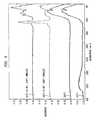
- FIG. 4is a FTIR spectrum of as deposited aluminum oxide films at various deposition temperatures.
- FIG. 5is a FTIR spectrum of as deposited or as deposited/annealed aluminum oxide films.
- FIG. 6is plot of capacitance, C, (pF) vs. voltage (V) showing high frequency (100 KHz) CV curves of Al oxide films with different thickness deposited at 500° C.
- FIG. 7is a plot of capacitance, C, (pF) vs. Voltage, V, for Al oxide films deposited at 600° C. and annealed in O 2 and forming gas.
- FIG. 8is a plot showing the IV characteristics of films deposited at 500° and 600° C.
- FIG. 9is a plot of t qm (nm) vs. t ph (nm) showing the dielectric constants of Al oxide films deposited at 500° C. and annealed in O 2 and forming gas.
- FIG. 10is a plot of the leakage current for various deposited and annealed aluminum oxide films.
- FIG. 11is a schematic representation of a delivery system for chemical vapor deposition or atomic layer deposition of a film or coating.
- FIGS. 12A-Hare illustrations of a cross-sectional view of a transistor containing a multilayer dielectric through various processing steps.
- FIGS. 13-22are illustrations of a cross-sectional view of the fabrication of a transistor.
- FIGS. 23-27are illustrations of a cross-sectional view of the fabrication of a stack capacitor.
- FIG. 28is an illustration of a cross-sectional view of a trench capacitor.
- the present inventionbroadly relates to CVD or ALD of aluminum oxide, and fabrication of an electronic devices incorporating a film deposited by the inventive method. More specifically, the present invention relates to CVD or ALD of aluminum oxide utilizing an aluminum alkoxide precursor dissolved, emulsified or suspended in a liquid, vaporizing the aluminum alkoxide precursor so as to form a vaporized precursor, and depositing a constituent of the vaporized precursor on a substrate to form a film at a deposition temperature of greater than 500° C. More particularly, the deposition is carried out at a temperature of from about 500° to about 1200° C. Following the deposition of the aluminum oxide film, the film may be annealed utilizing any conventional annealing process such as a forming gas anneal.
- the precursoris defined in the present invention as any aluminum alkoxide.
- a generalized formula for the precursor of the present inventionis Al(OR) 3 where R is a ligand selected from linear or branched C 1 -C 12 alkyls
- Ris a ligand selected from linear or branched C 1 -C 12 alkyls
- the preferred precursorsare aluminum iso-propoxide, aluminum sec-butoxide, aluminum ethoxide, aluminum iso-butoxide, aluminum methoxide, aluminum propoxide, aluminum butoxide, aluminum tertiary-butoxide, or aluminum phenoxide.
- the liquidis selected from aliphatic hydrocarbons, aromatic hydrocarbons, alcohols, ethers, aldehydes, ketones, acids, phenols, esters, amines, alkylnitriles, halgonated hydrocarbons, silylated hydrocarbons, thioethers, amines, cyanates, isocyanates, thiocyanates, silicone oils, nitroalkyls, alkylnitrates and/or mixtures of one or more of the above.
- the precursormay be dissolved, emulsified or suspended in the liquid using techniques well known to those skilled in the art.
- Vaporizationis carried out by heating the precursor and liquid to a temperature of from about 40° to about 250° C. for a time period sufficient to convert the liquid precursor into a vaporized precursor.
- the vaporizationmay be carried out in the presence of an inert gas such as He, N 2 or Ar, which gas may also be used during the deposition of the aluminum oxide.
- the method of aluminum oxide deposition of the present inventioncan be used in any CVD or ALD process with any delivery means using any number of co-reactants.
- the inventionis not limited to a specific CVD or ALD apparatus or delivery system.
- Chemical vapor deposition (CVD)is defined as introduction of multiple reagents into a reactor simultaneously.
- Atomic layer deposition (ALD)is defined as sequential introduction of multiple reagents into a reactor, including, but not limited to atomic layer epitaxy, digital chemical vapor deposition, pulsed chemical vapor deposition and other like methods.
- CMOScomplimentary metal oxide semiconductor
- the present inventionrelates to the fabrication of a CMOS integrated circuit containing both n-type field effect transistors (NFETs) and p-type field effect transistors (PFETs) formed on a single substrate.
- NFET device 11is formed on a p-type conductivity region 13 of substrate 10 and contains a gate electrode 14 formed on a gate dielectric 15 and a pair of n-type source/drain regions 16 formed on laterally opposite sides of gate electrode 14 is noted that the ohmic contacts are not shown in FIG. 1 .
- PFET device 17is formed on a n-type conductivity region 18 of substrate 10 and contains the gate electrode 19 formed on gate dielectric 15 and a pair of p-type conductivity source/drain regions 20 formed along opposite sidewalls of gate electrode 19 .
- the ohmic contactsare not shown.
- the NFET and PFET devicesare separated by shallow trench isolation 21 and by spacers 22 .
- gate dielectric 15incorporates aluminum oxide deposited by the inventive method.
- Another aspect of the present inventionrelates broadly to fabrication of a structure of an integrated circuit capacitor incorporating aluminum oxide deposited by the inventive method. More specifically, the present invention relates to the fabrication of a capacitor. As shown in FIG. 2, a typical capacitor is formed on a substrate 30 , connected by a plug 31 to a transistor, with a barrier 32 and consists of a bottom electrode 33 , a dielectric material 34 which may or may not be ferroelectric, and a top electrode 35 . In this aspect of the present invention, the dielectric material 34 incorporates aluminum oxide deposited by the inventive method.
- the capacitormay be stack or trench.
- a yet further aspect of the present inventionrelates broadly to fabrication of a structure of an integrated circuit wiring structure incorporating aluminum oxide deposited by the inventive method.
- a typical wiring structureis formed by etching trenches 41 and vias 42 into a dielectric layer 43 .
- a metal thin film wire 44 and a dielectric layer 45 of a wiring layerare filled with a barrier material 46 and a wiring metal 47 .
- the dielectric material 43 or 45incorporates aluminum oxide deposited by the inventive method.
- the aluminum oxide filmswere deposited in a quartz horizontal hot wall CVD reactor equipped with a 1 ⁇ 3 ⁇ 8′′ quartz flow cell.
- the aluminum alkoxide source mixturewas comprised of 40 grams of aluminum iso-propoxide, Al(i-OC 3 H 7 ) 3 , and 1 liter of iso-propanol.
- a thin layer (less than 20 ⁇ ) of SiO x N ywas deposited on a silicon wafer prior to growth of aluminum oxide.
- the aluminum alkoxide source mixturewas flowed at 0.2-0.05 ml/min, preferably 0.05 ml/min.
- the vaporizer temperaturewas 120-180° C., preferably 120° C.
- Anhydrous nitrogenwas, introduced into the vaporizer at 20-2000 sccm, preferably 200 sccm as a carrier gas for the volatilized aluminum iso-propoxide.
- a mixture of nitrogen and oxygenwas introduced through a separate inlet as the reactant gas.
- the system pressurewas 5 Torr during growth.
- the substratewas heated by an external high intensity infrared lamp and the susceptor was comprised of Hastalloy.
- the temperature of the susceptorwas monitored by insertion of a thermocouple into the susceptor.
- Aluminum oxidewas deposited at 350-700° C., preferably at temperatures of greater than 500° C.
- the aluminum oxide films deposited at 350° C. and 400° C.contained a broad absorption band at 3700-3000 cm ⁇ 1 which is assigned to O—H stretching vibrations of OH and H 2 O in the as deposited aluminum oxide films.
- deposition temperature of 500° C. and greaterno absorption band at 3700-3000 cm ⁇ 1 was observed.
- a distinctive narrow sharp strong absorptionwas observed at 581 cm ⁇ 1 in the spectra of aluminum oxide deposited at 350° C., 400° C., and 500° C.
- Aluminum oxide with similar absorption spectrahave been defined as ⁇ -Al 2 O 3 .
- 600° C.At a deposition temperature of 600° C.
- the as deposited filmswere annealed at 1000° C. for 30 min in oxygen. As shown in the FTIR spectra of the annealed films (FIG. 5 ), the aluminum oxide films deposited at 400° C. had strong absorptions assignable to SiO 2 .
- the strong absorptions at 1200 and 1080 cm ⁇ 1are ascribed to the LO and TO components of the asymmetric stretch of the SiO 4 unit, respectively.
- the absorption bands at 800 cm ⁇ 1 and 450 cm ⁇ 1are attributed to skeletal network Si—O—Si symmetric stretching and bond bending, respectively.
- the remaining absorption bandsare assigned to Al—O stretching and bending vibrations.
- the relative peak intensities and areas of the absorptions assigned to SiO 2 (1200, 1080, 800 and 450 cm ⁇ 1 )was reduced relative to the absorptions assigned to Al—O. It is believed that the aluminum oxide deposited at temperatures less than 500° C. which contain significant quantities of OH and/or absorbed water as observed in the FTIR spectra are less dense, contain an excess of oxygen and more readily allow the diffusion of oxygen through the film facilitating the formation of an interfacial oxide layer during post deposition annealing.
- Aluminum oxide filmswere analyzed for carbon content by nuclear reaction analysis (NRA).
- the sampleswere analyzed for total C and O using a 1.05 MeV beam of deuterons and the 16 O(d,p 1 ) 17 O* and 12 C(d,p 0 ) 13 C nuclear reactions.
- Each samplewas run three times to check its stability during irradiation. Due to the low stopping power of the particles and the large positive Q-values, these reactions have poor depth sensitivity, and cannot be used to directly separate contributions from the surface or substrate.
- a linear backgroundwas subtracted from the 16 O(d,p 1 ) 17 O* reaction peak in all spectra.
- a 1000 ⁇ SiO 2 standardwas used to normalize the oxygen data.
- reaction yieldis constant to within ⁇ 5% over this depth range, the average value was used to reduce the analysis to simple ratios of the reaction yields.
- a density of 2.3was assumed, to give an areal density for this standard of 4.6E17 16 O/cm 2 .
- a linear backgroundwas subtracted from the 12C(d,p 0 ) 13 C reaction peak in all spectra.
- a 20 microgram/cm 2 carbon foil on a Si substratewas used to normalize the carbon data.
- the reaction yieldis constant to within ⁇ 3% over this depth range, so as in the case of the oxygen analysis, an average value was used to simplify the analysis.
- the areal density used for this samplewas 1.0E18 12 C/cm 2 .
- capacitorswere formed by Al evaporation through a metal mask with the substrates held at room temperature. Prior to depositing the Al contacts the films were annealed in O 2 at 600° C. for 30 min and forming gas (FG) at 550° C. for 30 min. The area for these metal contacts was 5.4 ⁇ 10 ⁇ 4 cm ⁇ 3 .
- the capacitorswere fabricated on n-type Si substrates with P doping at about 1 ⁇ 10 15 cm ⁇ 3 .
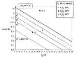
- FIG. 6shows a family of high frequency (100 KHz) CV curves of Al oxide films with different thickness deposited at 500° C.
- Kis normalized to the SiO 2 dielectric constant of 3.9, then the physical thickness is expressed as an equivalent thickness.
- low t eqare desirable.
- very high electric fieldsare generated at the interface with the result that the classical formula is not correct and should be corrected for quantum effects.
- MOSmetal oxide semiconductor
- non ideal flat band shiftsare observed in metal oxide semiconductor (MOS) capacitors because of non ideal conditions. Excessive charge in the films or at the oxide/Si interface can produce non ideal shifts. Also, different metals deposited on the oxide produce flat band shifts because of their inherent different work function values.
- flat bandoccurs for capacitance values below 100 pF.
- Flat band shift measured on the capacitor with low t qmis about ⁇ 0.6/0.7 V.
- some charge at the interface or in the bulk Al 2 O 3may exist.
- some hystersisis present in the CV characteristics, indicating undesirable film charge trapping.
- Dielectric constant values of the Al oxidewere measured by using a linear fit of the oxide quantum mechanical thickness extracted from CV characteristics versus the physical oxide thickness determined by n&k analysis (n&k Analyzer, n&k Technology, S. Clara, Calif.).
- the total capacitanceis represented by an interfacial SiO 2 capacitance in series with a high K dielectric film capacitance and using the parallel plate capacitor equation
- the equivalent quantum mechanical t qm (or classical t eq ) thickness versus the physical thickness t phcan be written as:
- t oxis the interfacial oxide thickness
- K ox3.9 (SiO 2 dielectric constant).
- the quantum mechanical thickness t qmwas calculated according to an IBM simulator, based on the “Lo et al.” reference, requiring the dot area and accumulation capacitance value at about 2.1 V. From the measured electrical and physical thickness values, the dielectric constant K qm and the residual interfacial layer R qm thickness were than extracted via equation (3), using a least square fitting procedure.
- Dielectric constantis about 10 and the residual SiO 2 layer about 1.3 nm.
- FIG. 7shows a family of CV curves for Al oxide films deposited at 600° C. and annealed in O 2 and FG as above.
- the curve with low t qmshows a flatband shift of about ⁇ 0.65 V which is about ⁇ 0.35 V from ideal when corrected for the Al work function.
- the hysterisis for the low t qm ( ⁇ 1.8) filmis very small ⁇ 10 mV.
- FIG. 7indicates that the residual interfacial layer may also be reduced to a few Angstroms when compared with the 500° C. process. In general, the 600° C. process produced better electrical performance than 500° C. because of the reduced hysterisis and reduced interfacial layer thickness.
- FIG. 8shows IV characteristics of films deposited at 500° C. and 600° C. The current densities at 1 V are plotted again in FIG. 10 .
- leakage reductionis about 3 orders of magnitude when compared with the equivalent SiO 2 oxide thickness.
- the 600° C. deposition processshow lower leakage than the 500° C. process where leakage reduction was only 15 times with respect to SiO 2 .
- the liquidis not vaporized and is diverted from the CVD or ALD reactor.
- the aluminum alkoxideis dissolved, emulsified or suspended in a liquid which vaporizes at a higher temperature.
- the aluminum alkoxide and the liquidis introduced into a vaporizer where the aluminum alkoxide is vaporized.
- the liquidis not vaporized, but instead is diverted from the reactor in liquid form.
- FIG. 11One possible apparatus configuration is shown in FIG. 11 .
- the aluminum alkoxide and liquid ( 102 )would flow from ampoule 100 to vaporizer 105 through outlet 104 .
- the aluminum alkoxideis volatilized in the vaporizer, but the liquid is not.
- the vaporized aluminum alkoxideis then transported to reactor 110 , and the nonvaporized inert liquid is drained out of the vaporizer and collected in trap 115 .
- the vaporizer temperatureis set at less than the boiling point of the liquid.
- One preferred methodwould be aluminum isopropoxide and dodecane (boiling point 216° C.) with the vaporizer temperature set at 120° C., and the deposition temperature greater than 500° C.
- a substrateis placed in a suitable reactor for atomic layer deposition, for example the commercial F-200 reactor made by Microchemistry, and an aluminum oxide film is deposited.
- Atomic layer depositionis performed in a cyclic fashion with sequential alternating pulses of vaporized aluminum alkoxide, reactant and purge gas (and/or vacuum evacuation of reactor chamber before introduction of aluminum alkoxide or reactant).
- the aluminum alkoxide source mixturewas comprised of 10 grams of aluminum iso-propoxide Al(i-OC 3 H 7 ) 3 and 1 liter of octane.
- the aluminum alkoxide sourceis vaporized in a vaporizer and the vapor is introduced into the reactor in a cyclical fashion.
- an oxidantis introduced including, but not limited to: oxygen, ozone, water, hydrogen peroxide, nitrous oxide and combinations thereof.
- the preferred oxidantis water.
- the vaporizer temperaturewas 120°-180° C., preferably 120° C.
- Aluminum oxidewas deposited at temperatures greater than 500° C.
- the aluminum alkoxide, reactant and inert purge gas(N 2 or Ar or other inert gas) are pulsed into the reactor in the following sequence:
- the aluminum alkoxide and reactant pulses(steps 1, and 3) last 0.1-1 second, preferably 0.5 seconds.
- the inert gas purge pulse (steps 2, and 4)last 0.2-5 seconds, preferably 2 seconds.
- Completion of steps 1-4is a cycle, the completion of 1 cycle results in deposition of about 0.4-2 monolayer of aluminum oxide or roughly 0.1 nm.
- the preferred thickness of deposited aluminum oxide containing filmis 50 nm, so 500 cycles of gas switching as described above are performed.
- the inventive methodis used to deposit aluminum oxide as gate dielectric layer 15 of the PFET and NFET as shown in FIG. 1.
- a Si wafer substrate containing patterned structuresis used. Selected regions of the substrate contain shallow trench isolation (STI) oxide located between the sites of transistor, other regions contain the field oxide, and selected regions of bare Si are exposed in the regions where transistor are to be located.
- the substrateis then placed in a suitable modular cluster tool, the surface of the bare Si is treated to form a SiO x N y layer in-situ without breaking vacuum, before a layer of aluminum oxide is deposited to a thickness of 1-100 nm using the CVD process of this invention.
- the waferis then transported to a second module of the modular cluster tool where the gate electrode can be deposited on the aluminum oxide in situ without breaking vacuum.
- the aluminum alkoxide source mixturewas composed of 40 grams of aluminum iso-propoxide in a liter of isopropanol.
- the aluminum alkoxide mixturewasp transported to a vaporizer where the mixture was vaporized at 120° C. and the vapor transported into the chemical vapor deposition module of the cluster tool where an oxidant including, but not limited to: oxygen, ozone, N 2 O, water, or mixtures thereof was present and an aluminum oxide film was deposited at 600° C.
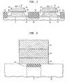
- the inventive methodis used to deposit a multilayer gate dielectric, 53 (See FIG. 12H) where at least one of the layers is aluminum oxide doped or undoped.
- a transistor deviceis formed on a conductivity region 54 and contains a gate electrode 52 formed on a gate dielectric 53 and a pair of n-type source/drain regions 51 formed on laterally opposite sides of gate electrode 52 .
- the multilayer gate dielectric 53is comprised of an optional upper layer, 57 which may act as a dopant diffusion barrier and stabilize the structure during deposition of the gate electrode 52 .
- An optional lower layer 55which may act as an electron barrier layer and as a layer to prevent oxidation of the underlying silicon during processing or both.
- the middle layer, 56is a high-K dielectric layer.
- a suitable lower layer 55is composed of dielectric materials including, but not limited to: SiO 2 , SiO x N y , or Si 3 N 4 , prepared from oxidation or nitridation of the silicon substrate or deposited separately. Other suitable lower layer materials include metal oxides or metal silicates.
- the high-K dielectric layer 56is selected from the group consisting of aluminum oxide or a multilayer structure where at least one of the layers is aluminum oxide.
- the dielectric materials comprising the multilayer structure with aluminum oxideare selected from the group including, but not limited to: Ta 2 O 5 , TiO 2 , ZrO 2 , HfO 2 , BaO, SrO, CaO, La 2 O 3 , Y 2 O 3 , yttrium alumnate, lathnaum alumnate, lanthanum silicate, yttrium silicate, hafnium silicate, zirconium silicate, doped or undoped mixtures, layers or combinations thereof.
- the multilayer structure with aluminum oxidemay be comprised of several layers of different materials such as a layer of hafnium oxide sandwiched between layers of aluminum oxide.
- the optional upper layer 57may be an oxidized or nitrided surface of the middle layer, 56 , or a deposited dielectric material including, but not limited to: SiO 2 , SiO x N y , Si 3 N 4 , ZrO 2 , HfO 2 , aluminum oxide, aluminosilicate, ytrrium silicate, zirconium silicate, hafnium silicate, lanthanum silicate doped or undoped mixtures, layers or combinations thereof.
- Preferred gate dielectricsare comprised of a lower layer of SiO x N y , a layer of aluminum oxide, and an upper barrier layer of nitrided aluminum oxide.
- the aluminum oxide in the gate dielectric 53is deposited by the inventive method.
- FIGS. 12A-12Hare cross sectional views showing one preferred means for fabrication of a transistor shown in FIG. 12H using the inventive method. Fabrication of the gate dielectric 53 is done in-situ in a cluster tool as manufactured by Applied Materials.
- a silicon substrate 50 with, a clean (no native SiO 2 ) surfaceis the starting point.
- the lower layer 55has been formed by oxidation/nitridation of the silicon substrate 50 to form a SiO x N y layer.
- a layer 56 of aluminum oxidehas been formed by the inventive method, comprised of depositing aluminum oxide by chemical vapor deposition at temperatures greater than 500° C.
- the upper layer 57is formed by plasma nitridation of the aluminum oxide surface.
- polysiliconis deposited as the gate electrode 52 .
- the gatesare formed, extension implant done, spacers 58 formed, and source/drain implants performed to produce a fully formed devices. The subsequent steps of contact formation, etc., are not shown.
- the inventive methodis used to fabricate a transistor using metal gates.
- a CMOS integrated circuit containing both n-type field effect transistors (NFETs) and p-type field effect transistors (PFETs)is formed on a single substrate 10 .
- NFET device 11is formed on a p-type conductivity region 13 of substrate 10 and contains a gate electrode 14 formed on a gate dielectric 15 and a pair of n-type source/drain regions 16 formed on laterally opposite sides of gate electrode 14 .
- PFET device 17is formed on a n-type conductivity region 18 of substrate 10 and contains the gate electrode 19 formed on gate dielectric 15 and a pair of p-type conductivity source/drain regions 20 formed along opposite sidewalls of gate electrode 19 .
- the NFET and PFET devicesare separated by shallow trench isolation 21 and by spacers 22 .
- the gate electrode 14 or 19is comprised of a bulk metal or alloy having the appropriate work function.
- Metals suitable for the gate electrode 14 of the NFET device 11include, but are not limited to: Al, Ag, Bi, Cd, Fe, Ga, Hf, In, Mn, Nb, Y, and Zr or alloys thereof.
- At least one metal suitable for the NFETmay also be alloyed with W, Mo, Cr, and Cu to form the gate electrode 14 .
- Metals suitable for the gate electrode 19 of the PFET device 17include, but are not limited to: Ni, Pt, Be, Ir, Te, Re and Rh. At least one metal suitable for the PFET may also be alloyed with W, Mo, Cr and Cu to form gate electrode 19 . The subsequent steps of contact formation, etc., are not described.
- the gate dielectric 15which is selected from the group consisting of aluminum oxide or a multilayer structure wherein at least one of the layers is aluminum oxide, is deposited by the inventive method.
- FIG. 22shows a generic device structure including NFETs and PFETs.
- NFET and PFETare formed on a single p-type conductive substrate 60 .
- NFET deviceis formed on a p-type conductivity region of substrate 60 and contains a gate electrode 62 formed on a gate dielectric 64 and a pair of n-type source/drain regions 65 formed on laterally opposite sides of gate electrode 62 .
- PFET deviceis formed on a n-type well 72 of substrate 60 isolated by shallow trench isolation 73 and contains the gate electrode 74 formed on gate dielectric 64 and a pair of p-type conductivity source/drain regions 76 formed along opposite sidewalls of gate electrode 74 .
- FIGS. 13 through 22are partial cross sectional views showing one example of a possible fabrication sequence for a standard CMOS flow.
- a silicon substrate 60 having shallow trench isolation (STI) 73 and an N-well 72are formed in a portion of a p-type conductive substrate.
- a gate dielectric 64 and a masking layer (for example Si 3 N 4 ) 77have been formed on the substrate.
- the gate dielectric 64may be deposited according to the inventive method.
- an opening in the masking layer 77 where the NFET gate will gohas been formed.
- the NFET gate electrode 62has been formed.
- Materials suitable for the NFET gate electrode 62include, but not limited to: polysilicon, W, Mo, Ti, Cr, Cu, Fe, Mn, Nb, V, Re, Pt, Ag, Bi, Cd, Fe, Ga, Hf, In, Mn, Y, Zr doped or undoped alloys, mixtures and multilayers thereof.
- the NFET gate electrode 62may be deposited by the inventive method. In FIG. 17, a chemical-mechanical polish (CMP) step has be done to planarize the surface. In FIGS. 18 through 20, steps are shown which repeat those in FIGS. 15-17 for the PFET device fabrication. In FIG. 18, an opening in the masking layer 77 where the PFET gate will go has been formed. In FIG.
- the PFET gate electrode 74has been formed.
- Materials suitable for the gate electrode 74 for PFETinclude, but not limited to: polysilicon, Ni, W, Mo, Ti, Cr, Te, Cu, Pd, Pt, Be, Au, Ir, Te, Rh, doped or undoped alloys, mixtures and multilayers thereof.
- the PFET gate electrode 74may be deposited by the inventive method.
- a chemical-mechanical polish (CMP) stephas be done to planarize the surface.
- extension implantsare performed, one for the NFET, and one for the PFET, each through a blocking layer.
- CMPchemical-mechanical polish
- source/drain implantsare performed, after a spacer 78 formation process, one for the NFET, and one for the PFET, each through a blocking layer to complete device fabrication. The subsequent steps of contact formation, etc. are not shown.
- the gate dielectric 64which is selected from the group consisting of aluminum oxide or a multilayer structure where at least one of the layers is aluminum oxide, is deposited by the inventive method.
- an integrated circuit capacitoris fabricated incorporating aluminum oxide deposited by the inventive method.
- a typical capacitoris formed on a substrate 30 , connected by a plug 31 to a transistor, with a barrier 32 and consists of a bottom electrode 33 , a dielectric material 34 which may or may not be ferroelectric, and a top electrode 35 .
- the dielectric material, 34 aluminum oxideis deposited by the inventive method.
- FIGS. 23 through 27are partial cross sectional views showing one example of a possible fabrication sequence for a capacitor.
- a substrate 30 having a trenchis formed.
- Substratesinclude, but are not limited to: Si-containing semiconductor substrates, silicon on insulator substrates, Ge substrates, SiGe substrates, GaAs substrates, and other like substrates, dielectrics, metals, organic substrates, glasses, metal oxides, plastic polymeric substrates and mixtures, combinations and layers thereof.
- a plug material 31 and an optional barrier 32is formed.
- the plug materialis composed of conventional conductive materials including, but not limited to: polysilicon, W, Mo, Ti, Cr, Cu, and may deposited utilizing the inventive method.
- the optional conductive barrier 32is composed of conventional conductive materials including, but not limited to: TaN, TaSiN, TiAlN, TiSiN, TaSiN, TaWN, TiWN, TaSiN, TaAlN, NbN, ZrN, TaTiN, TiSiN, TiAlN, IrO 2 , SiC, TiPt, TiNPt, TiAlN-Pt, Ru, RuO 2 , RuPt, RuO 2 , WSi, Ti, TiSi, doped and undoped polysilicon, Al, Pd, Ir, IrO x , Os, OsO x , MoSi, TiSi, ReO 2 , mixtures or multilayers thereof and may be deposited utilizing the inventive method.
- conventional conductive materialsincluding, but not limited to: TaN, TaSiN, TiAlN, TiSiN, TaSiN, TaWN, TiWN, TaSiN, TaAlN, NbN
- a bottom electrode 33is formed.
- the bottom electrodeis composed of conductive materials including, but not limited to: polysilicon, Ni, Pd, Pt, Cu, Ag, Au, Ru, Ir, Rh,IrO x , RuO x , TaN, TaSiN, Ta, SrRuO 3 , LaSrCoO 3 , doped or undoped alloys, mixtures, or multilayer thereof.
- a dielectric material 34is formed. The dielectric material is selected from the group consisting of aluminum oxide or a multilayer structure where at least one of the layers is aluminum oxide.
- the dielectric materials comprising the multilayer structure with aluminum oxideare selected from any insulating material including, but not limited to: SiO 2 , SiO x N y , Si 3 N 4 , metal oxides such as Ta 2 O 5 , TiO 2 , BaO, SrO, CaO, ZrO 2 , HfO 2 , La 2 O 3 , Y 2 O 3 alloys, mixtures or layers thereof, or multicomponent metal oxides such as pervoskite type oxide having the formula ABO 3 wherein B is at least one acid oxide containing a metal selected from the group consisting of Al, Ti, Zr, Hf, V, Nb, Ta, Cr, Mo, W and Cu, and A is at least one additional cation having a positive formal charge of from about 1 to about 3.
- metal oxidessuch as Ta 2 O 5 , TiO 2 , BaO, SrO, CaO, ZrO 2 , HfO 2 , La 2 O 3 , Y 2 O 3 alloys, mixtures or
- Examplesinclude, but are not limited to: barium strontium titanate, zirconate, or hafnate, lead titanate, yttrium alumnate, lanthanum alumnate, lead zirconium titanate, silicates such as hafnium silicate, zirconium silicate including rare earth doped silicates.
- a top electrode 35is formed.
- the top electrodeis composed of conductive materials including, but not limited to: polysilicon, Ni, Pd, Pt, Cu, Ag, Au, Ru, Ir, Rh,IrO x , RuO x , TaN, TaSiN, Ta, SrRuO 3 , LaSrCoO 3 , doped or undoped alloys, mixtures, or multilayer, thereof.
- the top and bottom electrodemay or may not be similar.
- the dielectric material 34which is selected from group consisting of aluminum oxide or multilayer structure wherein at least one of the layers is aluminum oxide, is deposited by the inventive method.
- an integrated circuit trench capacitoris fabricated incorporating at least one component deposited by the inventive method.
- One possible example for fabricating a trench capacitor on a substrate 30is shown in FIG. 28.
- a capacitor recessis formed in the substrate 30 which is connected to underlying circuitry via plug 31 .
- the circuitryis covered with a dielectric insulating layer (isolation dielectric) 83 .
- Substratesinclude, but are not limited to: Si-containing semiconductor substrates, silicon on insulator substrates; Ge substrates, SiGe substrates, GaAs substrates, and other like substrates, dielectrics, metals, organic substrates, glasses, metal oxides, plastic polymeric substrates and mixtures, combinations and layers thereof.
- the dielectric insulating layer (isolation dielectric) 83is selected from any insulating material including, but not limited to: SiO 2 , SiO x N y , Si 3 N 4 , phosphosilicate glass, or metal oxides such as aluminum oxide doped or undoped mixtures, or multilayers thereof.
- an optional conductive barrier layer 32 , bottom electrode layer 33 , dielectric layer 34 , and a top electrode layer 35 , and optional dielectric buffer layer 36is deposited in sequence, an optional conductive barrier layer 32 , bottom electrode layer 33 , dielectric layer 34 , and a top electrode layer 35 , and optional dielectric buffer layer 36 .
- the plug materialis composed of conventional conductive materials including, but not limited to: polysilicon, W, Mo, Ti, Cr, Cu, and may be deposited utilizing the inventive method.
- the optional conductive barrier 32is composed of conventional conductive materials including, but not limited to: TaN, TaSiN, TiAlN, TiSiN, TaSiN, TaWN, TiWN, TaSiN, TaAlN, NbN, ZrN, TaTiN.
- the bottom electrode 33is composed of conductive materials including, but not limited to: polysilicon, Ni, Pd, Pt, Cu, Ag, Au, Ru, Ir, Rh,IrO x , RuO x , TaN, TaSiN, Ta, SrRuO 3 , LaSrCoO 3 , doped or undoped alloys, mixtures, or multilayers thereof.
- the dielectric material, 34is selected from the group consisting of aluminum oxide or a multilayer structure where at least one of the layers is aluminum oxide.
- the dielectric materials comprising the multilayer structure with aluminum oxideare selected from any insulating material including, but not limited to: SiO 2 , SiO x N y , Si 3 N 4 , metal oxides such as Ta 2 O 5 , TiO 2 , BaO, SrO, CaO, ZrO 2 , HfO 2 , aluminum oxide, La 2 O 3 , Y 2 O 3 alloys, mixtures or layers thereof, or multicomponent metal oxides such as pervoskite type oxide having the formula ABO 3 wherein B is at least one acid oxide containing a metal selected from the group consisting of Al, Ti, Zr, Hf, V, Nb, Ta, Cr, Mo, W and Cu, and A is at least one additional cation having a positive formal charge of from about 1 to about 3.
- metal oxidessuch as Ta 2 O 5 , TiO 2 , BaO, SrO, CaO, ZrO 2 , HfO 2 , aluminum oxide, La 2 O 3 , Y 2 O 3
- the top electrode 35is composed of conductive materials including, but not limited to: polysilicon, Ni, Pd, Pt, Cu, Ag, Au, Ru, Ir, Rh,IrO x , RuO x , TaN, TaSiN, Ta, SrRuO 3 , LaSrCoO 3 , doped or undoped alloys, mixtures, or multilayer, thereof.
- the top and bottom electrodemay or may not be similar.
- the optional dielectric barrieris composed of any insulating material including, but not limited to: SiO 2 , SiO x N y , Si 3 N 4 , TiON, AlN, SiN, TiN; metal oxides such as Ta 2 O 5 , TiO 2 , ZrO 2 , HfO 2 , aluminum oxide, La 2 O 3 , Y 2 O 3 , alloys, mixtures or layers thereof, or multicomponent metal oxides.
- the sequentially deposited layersare planarized to yield a trench capacitor in the capacitor recess.
- An insulating passivation layer 37 and an inter-layer dielectric layer 38are deposited to form a barrier structure over the trench capacitor in the capacitor recess.
- the insulating passivation layer 37is composed of any insulating material including, but not limited to: SiO 2 , SiO x N y , Si 3 N 4 , TiON, AlN, SiN, TiN, metal oxides such as Ta 2 O 5 , TiO 2 , ZrO 2 , HfO 2 , aluminum oxide, La 2 O 3 , Y 2 O 3 , alloys, mixtures or layers thereof, or multicomponent metal oxides.
- the inter-layer dielectric 38is selected from any insulating material including, but not limited to: SiO 2 , SiO x N y , Si 3 N 4 , phosphosilicate glass, or metal oxides such as aluminum oxide doped or undoped mixtures, or multilayer, thereof.
- a viais formed in the barrier structure.
- a diffusion barrier layer 81 and a metallization layer 82are deposited over the barrier structure and via.
- the diffusion barrier layer 81includes, but not limited to: WN, TiN, or TaN.
- the metallization layer 82is selected from any conductive material including, but not limited to: Al, W, Mo, Ti, Cr, or Cu doped or undoped alloys, mixtures, or layers thereof.
- the dielectric material 34which is selected from the group consisting of aluminum oxide or a multilayer structure wherein at least one of the layers is aluminum oxide, is deposited by the inventive method; optionally aluminum oxide may be utilized as the dielectric including, but not limited to insulating passivation layer, inter-layer dielectric, diffusion barrier layer, isolation dielectric.
- an integrated circuit wiring structureis fabricated incorporating at least one component deposited by the inventive method.
- a typical wiring structureis formed by etching trenches 41 and vias 42 into a dielectric layer 43 selected from the group consisting of aluminum oxide or multilayer structures with aluminum oxide.
- the multilayer structures with aluminum oxidemay consist of one or more layers selected from the group consisting of SiO 2 , SiO x N y , Si 3 N 4 , phosphosilicate glass, or metal oxides doped or undoped mixtures, or multilayers thereof.
- the metallization layermay be patterned by a damascene or a dual damascene process or by lithography and etching.
- a metal thin film wire 44selected from any conductive material including, but not limited to: Al, W, Mo, Ti, Cr, or Cu alloys, mixtures, or layers thereof, and a dielectric layer 45 selected from the group consisting of aluminum oxide or multilayer structures with aluminum oxide.
- the multilayer structures with aluminum oxidemay consist of one or more layers selected from the group consisting SiO 2 , SiO x N y , Si 3 N 4 , phosphosilicate glass; or metal oxides such as aluminum oxide doped or undoped mixtures, or multilayers thereof.
- the trench and viaare filled with a barrier material 46 , including, but not limited to: WN, TiN, or TaN and a wiring metal 47 selected from any conductive material including, but not limited to: Al, W, Mo, Ti, Cr, or Cu doped or undoped alloys, mixtures, or layers thereof.
- a barrier material 46including, but not limited to: WN, TiN, or TaN and a wiring metal 47 selected from any conductive material including, but not limited to: Al, W, Mo, Ti, Cr, or Cu doped or undoped alloys, mixtures, or layers thereof.
- the dielectric layer 43 or 45contains aluminum oxide deposited by the inventive method.
Landscapes
- Chemical & Material Sciences (AREA)
- Engineering & Computer Science (AREA)
- Chemical Kinetics & Catalysis (AREA)
- General Physics & Mathematics (AREA)
- Manufacturing & Machinery (AREA)
- Computer Hardware Design (AREA)
- Microelectronics & Electronic Packaging (AREA)
- Power Engineering (AREA)
- Condensed Matter Physics & Semiconductors (AREA)
- General Chemical & Material Sciences (AREA)
- Physics & Mathematics (AREA)
- Materials Engineering (AREA)
- Mechanical Engineering (AREA)
- Metallurgy (AREA)
- Organic Chemistry (AREA)
- Crystallography & Structural Chemistry (AREA)
- Inorganic Chemistry (AREA)
- Chemical Vapour Deposition (AREA)
- Insulated Gate Type Field-Effect Transistor (AREA)
- Formation Of Insulating Films (AREA)
Abstract
Description
| TABLE 1 |
| Carbon content of aluminum oxide films as |
| determined by nuclear reaction analysis. |
| Tdeposition | thickness | As Reacted | Annealed | ||
| ° C. | nm | atomic % C | atomic % C | ||
| 350 | 1,626 | 1.4 | 1.5 | ||
| 0 | 732 | 1 | 0.8 | ||
| 375 | 343 | 1 | 0.9 | ||
| 400 | 979 | 1.2 | 1.4 | ||
| 400 | 400 | 1 | 1.1 | ||
| 500 | 1,019 | 0.2 | 0.2 | ||
| 600 | 1,280 | 0.06 | 0.03 | ||
Claims (10)
Priority Applications (2)
| Application Number | Priority Date | Filing Date | Title |
|---|---|---|---|
| US09/676,882US6664186B1 (en) | 2000-09-29 | 2000-09-29 | Method of film deposition, and fabrication of structures |
| US10/674,961US7015152B2 (en) | 2000-09-29 | 2003-09-30 | Method of film deposition, and fabrication of structures |
Applications Claiming Priority (1)
| Application Number | Priority Date | Filing Date | Title |
|---|---|---|---|
| US09/676,882US6664186B1 (en) | 2000-09-29 | 2000-09-29 | Method of film deposition, and fabrication of structures |
Related Child Applications (1)
| Application Number | Title | Priority Date | Filing Date |
|---|---|---|---|
| US10/674,961DivisionUS7015152B2 (en) | 2000-09-29 | 2003-09-30 | Method of film deposition, and fabrication of structures |
Publications (1)
| Publication Number | Publication Date |
|---|---|
| US6664186B1true US6664186B1 (en) | 2003-12-16 |
Family
ID=29712544
Family Applications (2)
| Application Number | Title | Priority Date | Filing Date |
|---|---|---|---|
| US09/676,882Expired - LifetimeUS6664186B1 (en) | 2000-09-29 | 2000-09-29 | Method of film deposition, and fabrication of structures |
| US10/674,961Expired - Fee RelatedUS7015152B2 (en) | 2000-09-29 | 2003-09-30 | Method of film deposition, and fabrication of structures |
Family Applications After (1)
| Application Number | Title | Priority Date | Filing Date |
|---|---|---|---|
| US10/674,961Expired - Fee RelatedUS7015152B2 (en) | 2000-09-29 | 2003-09-30 | Method of film deposition, and fabrication of structures |
Country Status (1)
| Country | Link |
|---|---|
| US (2) | US6664186B1 (en) |
Cited By (58)
| Publication number | Priority date | Publication date | Assignee | Title |
|---|---|---|---|---|
| US20020024080A1 (en)* | 2000-08-31 | 2002-02-28 | Derderian Garo J. | Capacitor fabrication methods and capacitor constructions |
| US20020025628A1 (en)* | 2000-08-31 | 2002-02-28 | Derderian Garo J. | Capacitor fabrication methods and capacitor constructions |
| US20020090777A1 (en)* | 2001-01-05 | 2002-07-11 | Leonard Forbes | Methods of forming capacitor structures, and capacitor structures |
| US20020094632A1 (en)* | 2000-08-31 | 2002-07-18 | Agarwal Vishnu K. | Capacitor fabrication methods and capacitor constructions |
| US20020106536A1 (en)* | 2001-02-02 | 2002-08-08 | Jongho Lee | Dielectric layer for semiconductor device and method of manufacturing the same |
| US20020182385A1 (en)* | 2001-05-29 | 2002-12-05 | Rensselaer Polytechnic Institute | Atomic layer passivation |
| US20020192974A1 (en)* | 2001-06-13 | 2002-12-19 | Ahn Kie Y. | Dielectric layer forming method and devices formed therewith |
| US20030098489A1 (en)* | 2001-11-29 | 2003-05-29 | International Business Machines Corporation | High temperature processing compatible metal gate electrode for pFETS and methods for fabrication |
| US20030178674A1 (en)* | 2002-03-22 | 2003-09-25 | Shigeru Fujita | Semiconductor device and its manufacturing method |
| US20030201034A1 (en)* | 2002-04-25 | 2003-10-30 | Marsh Eugene P. | Metal layer forming methods and capacitor electrode forming methods |
| US20040009679A1 (en)* | 2001-01-19 | 2004-01-15 | Yeo Jae-Hyun | Method of forming material using atomic layer deposition and method of forming capacitor of semiconductor device using the same |
| US20040026784A1 (en)* | 2002-08-08 | 2004-02-12 | O'kane William Jude | Combined atomic layer deposition and damascene processing for definition of narrow trenches |
| US20040043634A1 (en)* | 2002-08-28 | 2004-03-04 | Micron Technology, Inc | Systems and methods for forming metal-doped alumina |
| US20040043635A1 (en)* | 2002-08-28 | 2004-03-04 | Micron Technology, Inc. | Systems and methods for forming metal oxides using metal diketonates and/or ketoimines |
| US20040043625A1 (en)* | 2002-08-28 | 2004-03-04 | Micron Technology, Inc. | Systems and methods for forming metal oxides using metal compounds containing aminosilane ligands |
| US20040051117A1 (en)* | 2002-07-02 | 2004-03-18 | Oliver Chyan | Method of using materials based on Ruthenium and Iridium and their oxides, as a Cu diffusion barrier, and integrated circuits incorporating same |
| US20040152255A1 (en)* | 2002-11-29 | 2004-08-05 | Harald Seidl | Capacitor with electrodes made of ruthenium and method for patterning layers made of ruthenium or ruthenium(IV) oxide |
| US20040155348A1 (en)* | 2002-12-30 | 2004-08-12 | Dongbu Electronics Co., Ltd. | Barrier structure for copper metallization and method for the manufacture thereof |
| US20040194691A1 (en)* | 2001-07-18 | 2004-10-07 | George Steven M | Method of depositing an inorganic film on an organic polymer |
| US20040266126A1 (en)* | 2003-06-30 | 2004-12-30 | Lee Kee-Jeung | Method for manufacturing semiconductor capacitor having double dielectric layer therein |
| US20050062136A1 (en)* | 2001-01-26 | 2005-03-24 | Yoshihide Senzaki | Multilayer high k dielectric films and method of making the same |
| US20050106798A1 (en)* | 2001-09-14 | 2005-05-19 | Hynix Semiconductor Inc. | Semiconductor device and method for fabricating the same |
| US20050110115A1 (en)* | 2003-11-22 | 2005-05-26 | Hynix Semiconductor Inc. | Capacitor with hafnium oxide and aluminum oxide alloyed dielectric layer and method for fabricating the same |
| US20050130326A1 (en)* | 2003-12-10 | 2005-06-16 | Hynix Semiconductor Inc. | Method for fabricating capacitor in semiconductor device |
| US20050142715A1 (en)* | 2003-12-26 | 2005-06-30 | Fujitsu Limited | Semiconductor device with high dielectric constant insulator and its manufacture |
| US20050151184A1 (en)* | 2001-02-02 | 2005-07-14 | Lee Jong-Ho | Dielectric layer for semiconductor device and method of manufacturing the same |
| US20050189587A1 (en)* | 2004-02-27 | 2005-09-01 | Gordon Ma | LDMOS transistor |
| US20050239297A1 (en)* | 2003-09-30 | 2005-10-27 | Yoshihide Senzaki | Growth of high-k dielectrics by atomic layer deposition |
| US20050269669A1 (en)* | 2003-07-21 | 2005-12-08 | Mcclure Brent A | Capacitor constructions and methods of forming |
| US20060081948A1 (en)* | 2004-10-19 | 2006-04-20 | Ha-Jin Lim | Transistors with multilayered dielectric films and methods of manufacturing such transistors |
| US20060093841A1 (en)* | 2004-11-03 | 2006-05-04 | Samsung Electronics Co., Ltd. | Method of forming ferroelectric thin film |
| US20060097305A1 (en)* | 2004-11-08 | 2006-05-11 | Lee Kee-Jeung | Capacitor with zirconium oxide and method for fabricating the same |
| US20060124987A1 (en)* | 2002-12-30 | 2006-06-15 | Samsung Electronics Co., Ltd | Capacitor of semiconductor device and method for manufacturing the same |
| US7129580B1 (en) | 2001-04-17 | 2006-10-31 | Genus, Inc. | Methods and procedures for engineering of composite conductive films by atomic layer deposition |
| US20060264066A1 (en)* | 2005-04-07 | 2006-11-23 | Aviza Technology, Inc. | Multilayer multicomponent high-k films and methods for depositing the same |
| US20060269667A1 (en)* | 2005-04-29 | 2006-11-30 | Ce Ma | Method and apparatus for using solution based precursors for atomic layer deposition |
| US7160578B2 (en) | 2004-03-10 | 2007-01-09 | Pilkington North America | Method for depositing aluminum oxide coatings on flat glass |
| US7164203B1 (en) | 2001-04-17 | 2007-01-16 | Genus, Inc. | Methods and procedures for engineering of composite conductive by atomic layer deposition |
| US20070148897A1 (en)* | 2005-12-27 | 2007-06-28 | Hynix Semiconductor Inc. | Method for fabricating capacitor in semiconductor device |
| US20070161214A1 (en)* | 2006-01-06 | 2007-07-12 | International Business Machines Corporation | High k gate stack on III-V compound semiconductors |
| US20080138503A1 (en)* | 2004-12-23 | 2008-06-12 | Hynix Semiconductor Inc. | Method For Forming Dielectric Film And Method For Forming Capacitor In Semiconductor Device Using The Same |
| US20080182101A1 (en)* | 2003-05-16 | 2008-07-31 | Peter Francis Carcia | Barrier films for plastic substrates fabricated by atomic layer deposition |
| US20090260669A1 (en)* | 2008-04-21 | 2009-10-22 | International Business Machines Corporation | Metal-gate thermocouple |
| US20100143710A1 (en)* | 2008-12-05 | 2010-06-10 | Lotus Applied Technology, Llc | High rate deposition of thin films with improved barrier layer properties |
| US7825043B2 (en) | 2005-11-28 | 2010-11-02 | Hynix Semiconductor Inc. | Method for fabricating capacitor in semiconductor device |
| US20100288996A1 (en)* | 2002-12-19 | 2010-11-18 | Herner S Brad | Memory arrays including memory levels that share conductors, and methods of forming such memory arrays |
| US20110159204A1 (en)* | 2009-12-29 | 2011-06-30 | Lotus Applied Technology, Llc | Oxygen radical generation for radical-enhanced thin film deposition |
| US20110169378A1 (en)* | 2010-01-09 | 2011-07-14 | Seiko Epson Corporation | Actuator apparatus and methods of manufacturing actuator apparatus, liquid ejecting head, and liquid ejecting apparatus |
| US20120201860A1 (en)* | 2009-05-11 | 2012-08-09 | Weimer Alan W | Ultra-thin metal oxide and carbon-metal oxide films prepared by atomic layer deposition (ALD) |
| US20130140646A1 (en)* | 2002-08-26 | 2013-06-06 | Round Rock Research, Llc | Transistor with reduced depletion field width |
| US20130292835A1 (en)* | 2011-12-20 | 2013-11-07 | Sean King | Conformal low temperature hermetic dielectric diffusion barriers |
| US20140008799A1 (en)* | 2012-07-04 | 2014-01-09 | National Applied Research Laboratories | Method for fabricating metal line and device with metal line |
| US8737110B2 (en) | 2007-03-27 | 2014-05-27 | Sandisk 3D Llc | Large array of upward pointing P-I-N diodes having large and uniform current |
| US9881972B2 (en)* | 2016-05-20 | 2018-01-30 | Micron Technology, Inc. | Array of memory cells and methods of forming an array of memory cells |
| US10461128B2 (en) | 2017-04-26 | 2019-10-29 | Micron Technology, Inc. | Arrays of memory cells and methods of forming an array of elevationally-outer-tier memory cells and elevationally-inner-tier memory cells |
| CN113026000A (en)* | 2021-04-02 | 2021-06-25 | 泰杋科技股份有限公司 | Device and method for preparing tantalum nitride film by precursor coating gas protection laser |
| US11158721B2 (en)* | 2019-08-30 | 2021-10-26 | Taiwan Semiconductor Manufacturing Co., Ltd. | Metal oxide interlayer structure for nFET and pFET |
| CN116426904A (en)* | 2023-04-21 | 2023-07-14 | 广州天极电子科技股份有限公司 | A kind of aluminum oxide substrate for thin film circuit and its preparation method and application |
Families Citing this family (37)
| Publication number | Priority date | Publication date | Assignee | Title |
|---|---|---|---|---|
| JP4492783B2 (en)* | 2001-09-12 | 2010-06-30 | 日本電気株式会社 | Semiconductor device and manufacturing method thereof |
| US6773984B2 (en)* | 2002-08-29 | 2004-08-10 | Micron Technology, Inc. | Methods of depositing noble metals and methods of forming capacitor constructions |
| JP2005085822A (en)* | 2003-09-04 | 2005-03-31 | Toshiba Corp | Semiconductor device |
| KR100639673B1 (en)* | 2003-12-22 | 2006-10-30 | 삼성전자주식회사 | Semiconductor device having a gate dielectric film made of a high-k alloy and a method of manufacturing the same |
| KR100642635B1 (en)* | 2004-07-06 | 2006-11-10 | 삼성전자주식회사 | Semiconductor Integrated Circuits Having Hybrid Dielectric Films and Manufacturing Methods Thereof |
| US20060060930A1 (en)* | 2004-09-17 | 2006-03-23 | Metz Matthew V | Atomic layer deposition of high dielectric constant gate dielectrics |
| JP4543378B2 (en)* | 2004-11-15 | 2010-09-15 | エルピーダメモリ株式会社 | Manufacturing method of semiconductor device |
| US20060121742A1 (en)* | 2004-12-07 | 2006-06-08 | Intel Corporation | Method for making a semiconductor device having a high-k gate dielectric |
| US7316962B2 (en)* | 2005-01-07 | 2008-01-08 | Infineon Technologies Ag | High dielectric constant materials |
| US7078285B1 (en) | 2005-01-21 | 2006-07-18 | Sony Corporation | SiGe nickel barrier structure employed in a CMOS device to prevent excess diffusion of nickel used in the silicide material |
| KR100695150B1 (en)* | 2005-05-12 | 2007-03-14 | 삼성전자주식회사 | Transistor using metal-insulator conversion material and manufacturing method thereof |
| KR100687760B1 (en)* | 2005-10-19 | 2007-02-27 | 한국전자통신연구원 | Insulator having rapid metal-insulator transition and manufacturing method thereof, device using the same |
| KR100755373B1 (en)* | 2006-09-15 | 2007-09-04 | 삼성전자주식회사 | A contact structure having a conductive oxide film, a ferroelectric memory device adopting the same and methods of manufacturing the same |
| KR100819002B1 (en)* | 2006-10-20 | 2008-04-02 | 삼성전자주식회사 | Nonvolatile Memory Device Manufacturing Method |
| KR100875034B1 (en)* | 2007-01-02 | 2008-12-19 | 주식회사 하이닉스반도체 | Dielectric Film Formation Method of Flash Memory Device |
| US20080268154A1 (en)* | 2007-04-30 | 2008-10-30 | Shreyas Kher | Methods for depositing a high-k dielectric material using chemical vapor deposition process |
| JP2009027017A (en)* | 2007-07-20 | 2009-02-05 | Elpida Memory Inc | Insulator film, capacitor element, DRAM and semiconductor device |
| EP2188413B1 (en)* | 2007-09-07 | 2018-07-11 | Fujifilm Manufacturing Europe B.V. | Method for atomic layer deposition using an atmospheric pressure glow discharge plasma |
| JP5737941B2 (en)* | 2007-11-02 | 2015-06-17 | アイピーディーアイエイ | Multilayer structure and manufacturing method thereof |
| FI20070991L (en)* | 2007-12-19 | 2009-06-20 | Beneq Oy | Glass product, product use and manufacturing method |
| US7821081B2 (en)* | 2008-06-05 | 2010-10-26 | International Business Machines Corporation | Method and apparatus for flatband voltage tuning of high-k field effect transistors |
| TW201003915A (en)* | 2008-07-09 | 2010-01-16 | Nanya Technology Corp | Transistor device |
| US8163343B2 (en)* | 2008-09-03 | 2012-04-24 | Applied Materials, Inc. | Method of forming an aluminum oxide layer |
| US8778754B2 (en)* | 2008-09-15 | 2014-07-15 | Taiwan Semiconductor Manufacturing Company, Ltd. | Method of forming a single metal that performs N and P work functions in high-K/metal gate devices |
| US8067815B2 (en)* | 2008-12-11 | 2011-11-29 | Macronix International Co., Lt.d. | Aluminum copper oxide based memory devices and methods for manufacture |
| US8637390B2 (en)* | 2010-06-04 | 2014-01-28 | Applied Materials, Inc. | Metal gate structures and methods for forming thereof |
| US20120241865A1 (en)* | 2011-03-21 | 2012-09-27 | Nanya Technology Corporation | Integrated circuit structure |
| KR101901721B1 (en)* | 2011-07-26 | 2018-09-28 | 미쯔비시 가스 케미칼 컴파니, 인코포레이티드 | Etchant for copper/molybdenum-based multilayer thin film |
| JP6136573B2 (en)* | 2013-05-27 | 2017-05-31 | 富士通株式会社 | Semiconductor device and manufacturing method of semiconductor device |
| US8927439B1 (en)* | 2013-07-22 | 2015-01-06 | Rohm And Haas Electronic Materials Llc | Organoaluminum materials for forming aluminum oxide layer from coating composition that contains organic solvent |
| CN103700699A (en)* | 2013-12-19 | 2014-04-02 | 深圳市华星光电技术有限公司 | Gate metal structure and manufacturing method thereof |
| US9922884B2 (en) | 2015-10-14 | 2018-03-20 | International Business Machines Corporation | Integrated circuit with replacement gate stacks and method of forming same |
| KR102649437B1 (en)* | 2018-05-30 | 2024-03-19 | 한양대학교 산학협력단 | Anti-growth thin film and fabricating method of the same |
| WO2020141731A1 (en)* | 2018-12-31 | 2020-07-09 | 한양대학교 산학협력단 | Method for manufacturing metalless thin film, method for manufacturing micro-pattern, and method for manufacturing electronic element |
| US11211470B2 (en)* | 2019-10-18 | 2021-12-28 | Taiwan Semiconductor Manufacturing Company, Ltd. | Semiconductor device and method |
| KR102224067B1 (en)* | 2020-01-09 | 2021-03-08 | 주식회사 이지티엠 | Method of depositing thin films using protective material |
| JP2024129608A (en)* | 2023-03-13 | 2024-09-27 | 株式会社Flosfia | LAMINATED STRUCTURE AND SEMICONDUCTOR DEVICE |
Citations (6)
| Publication number | Priority date | Publication date | Assignee | Title |
|---|---|---|---|---|
| US4097314A (en) | 1976-12-30 | 1978-06-27 | Rca Corp. | Method of making a sapphire gate transistor |
| US5431734A (en) | 1994-04-28 | 1995-07-11 | International Business Machines Corporation | Aluminum oxide low pressure chemical vapor deposition (LPCVD) system-fourier transform infrared (FTIR) source chemical control |
| US5540777A (en) | 1994-09-30 | 1996-07-30 | International Business Machines Corporation | Aluminum oxide LPCVD system |
| US5728222A (en) | 1994-09-30 | 1998-03-17 | International Business Machines Corporation | Apparatus for chemical vapor deposition of aluminum oxide |
| US6037003A (en)* | 1996-10-16 | 2000-03-14 | President And Fellows Of Harvard College | Chemical vapor deposition of aluminum oxide |
| US6312565B1 (en)* | 2000-03-23 | 2001-11-06 | Agere Systems Guardian Corp. | Thin film deposition of mixed metal oxides |
Family Cites Families (1)
| Publication number | Priority date | Publication date | Assignee | Title |
|---|---|---|---|---|
| US5312565A (en)* | 1990-08-28 | 1994-05-17 | E. I. Dupont De Nemours And Company | Nonlinear optical materials |
- 2000
- 2000-09-29USUS09/676,882patent/US6664186B1/ennot_activeExpired - Lifetime
- 2003
- 2003-09-30USUS10/674,961patent/US7015152B2/ennot_activeExpired - Fee Related
Patent Citations (7)
| Publication number | Priority date | Publication date | Assignee | Title |
|---|---|---|---|---|
| US4097314A (en) | 1976-12-30 | 1978-06-27 | Rca Corp. | Method of making a sapphire gate transistor |
| US5431734A (en) | 1994-04-28 | 1995-07-11 | International Business Machines Corporation | Aluminum oxide low pressure chemical vapor deposition (LPCVD) system-fourier transform infrared (FTIR) source chemical control |
| US5540777A (en) | 1994-09-30 | 1996-07-30 | International Business Machines Corporation | Aluminum oxide LPCVD system |
| US5648113A (en) | 1994-09-30 | 1997-07-15 | International Business Machines Corporation | Aluminum oxide LPCVD system |
| US5728222A (en) | 1994-09-30 | 1998-03-17 | International Business Machines Corporation | Apparatus for chemical vapor deposition of aluminum oxide |
| US6037003A (en)* | 1996-10-16 | 2000-03-14 | President And Fellows Of Harvard College | Chemical vapor deposition of aluminum oxide |
| US6312565B1 (en)* | 2000-03-23 | 2001-11-06 | Agere Systems Guardian Corp. | Thin film deposition of mixed metal oxides |
Non-Patent Citations (8)
| Title |
|---|
| Eble, R., et al., "Low Temperature Aluminum Oxide Deposition Using Trimethylaluminum", Journal of Electronic Materials, vol. 12, No. 3, pp. 587-601, (1983). |
| Fournier, J., et al., "Preparation and Characterization of Thin Films of Alumina by Metal-Organic Chemical Vapor Deposition", Mat. Res. Bull. vol. 23, pp. 31-36, 1988. |
| Kim, J.S., et al., "Fabrication of aluminum oxide thin films by a low-pressure metalorganic chemical vapor deposition technique", App. Phys. Lett., 62(7), Feb. 15, 1993. |
| Klein, T.M., et al., "Evidence of aluminum silicate formation during chemical vapor deposition of amorphous Al2O3 thin films on Si(100)", Applied Physics Letters, vol. 75, No. 25, pp. 4001-4003, 1999. |
| Lo, S.-H, et al., "Quantum-Mechanical Modeling of Electron Tunneling Current from the Inversion Layer of Ultra-Thin-Oxide nMOSFET's", IEEE Electron Device Letters, vol. 18, No. 5, pp. 209-211, May 1997. |
| Mutoh, H., et al., "Multilayer Metallization with Planar Interconnect Structure Utilizing CVD Al2O3 Film", J. Electrochem.Soc.: Solid-State Science and Technology, vol. 12, No. 7, pp. 987-992, Jul. 1975. |
| Yom et al (Growth of Alumina thin films on silicon by low pressure MOCVD), 1991, pp. 72-75.** |
| Yom, S.S., et al., "Growth of -Al2O3 thin films on silicon by low pressure metal-organic chemical vapour deposition", Elsevier Sequoia, 213, pp. 72-75, 1992. |
Cited By (162)
| Publication number | Priority date | Publication date | Assignee | Title |
|---|---|---|---|---|
| US20070007572A1 (en)* | 2000-08-31 | 2007-01-11 | Agarwal Vishnu K | Capacitor fabrication methods and capacitor constructions |
| US20020025628A1 (en)* | 2000-08-31 | 2002-02-28 | Derderian Garo J. | Capacitor fabrication methods and capacitor constructions |
| US20020024080A1 (en)* | 2000-08-31 | 2002-02-28 | Derderian Garo J. | Capacitor fabrication methods and capacitor constructions |
| US20020094632A1 (en)* | 2000-08-31 | 2002-07-18 | Agarwal Vishnu K. | Capacitor fabrication methods and capacitor constructions |
| US7112503B1 (en) | 2000-08-31 | 2006-09-26 | Micron Technology, Inc. | Enhanced surface area capacitor fabrication methods |
| US7288808B2 (en) | 2000-08-31 | 2007-10-30 | Micron Technology, Inc. | Capacitor constructions with enhanced surface area |
| US7109542B2 (en) | 2000-08-31 | 2006-09-19 | Micron Technology, Inc. | Capacitor constructions having a conductive layer |
| US20070178640A1 (en)* | 2000-08-31 | 2007-08-02 | Derderian Garo J | Capacitor fabrication methods and capacitor constructions |
| US7053432B2 (en)* | 2000-08-31 | 2006-05-30 | Micron Technology, Inc. | Enhanced surface area capacitor fabrication methods |
| US7166883B2 (en)* | 2001-01-05 | 2007-01-23 | Micron Technology, Inc. | Capacitor structures |
| US20050026355A1 (en)* | 2001-01-05 | 2005-02-03 | Leonard Forbes | Capacitor structures |
| US7192827B2 (en) | 2001-01-05 | 2007-03-20 | Micron Technology, Inc. | Methods of forming capacitor structures |
| US20020164852A1 (en)* | 2001-01-05 | 2002-11-07 | Leonard Forbes | Capacitor structures |
| US20050167723A1 (en)* | 2001-01-05 | 2005-08-04 | Leonard Forbes | Capacitor structures |
| US20020090777A1 (en)* | 2001-01-05 | 2002-07-11 | Leonard Forbes | Methods of forming capacitor structures, and capacitor structures |
| US20040009679A1 (en)* | 2001-01-19 | 2004-01-15 | Yeo Jae-Hyun | Method of forming material using atomic layer deposition and method of forming capacitor of semiconductor device using the same |
| US7087482B2 (en)* | 2001-01-19 | 2006-08-08 | Samsung Electronics Co., Ltd. | Method of forming material using atomic layer deposition and method of forming capacitor of semiconductor device using the same |
| US20060234517A1 (en)* | 2001-01-19 | 2006-10-19 | Yeo Jae-Hyun | Method of forming material using atomic layer deposition and method of forming capacitor of semiconductor device using the same |
| US7425514B2 (en) | 2001-01-19 | 2008-09-16 | Samsung Electronics Co., Ltd. | Method of forming material using atomic layer deposition and method of forming capacitor of semiconductor device using the same |
| US20050062136A1 (en)* | 2001-01-26 | 2005-03-24 | Yoshihide Senzaki | Multilayer high k dielectric films and method of making the same |
| US20050074982A1 (en)* | 2001-02-02 | 2005-04-07 | Samsung Electronics Co., Ltd. | Dielectric layer for semiconductor device and method of manufacturing the same |
| US7902019B2 (en) | 2001-02-02 | 2011-03-08 | Samsung Electronics Co., Ltd. | Dielectric layer for semiconductor device and method of manufacturing the same |
| US20080185631A1 (en)* | 2001-02-02 | 2008-08-07 | Samsung Electronics Co., Ltd. | Dielectric layer for semiconductor device and method of manufacturing the same |
| US6844604B2 (en)* | 2001-02-02 | 2005-01-18 | Samsung Electronics Co., Ltd. | Dielectric layer for semiconductor device and method of manufacturing the same |
| US7112539B2 (en) | 2001-02-02 | 2006-09-26 | Samsung Electronic Co., Ltd. | Dielectric layer for semiconductor device and method of manufacturing the same |
| US7371633B2 (en)* | 2001-02-02 | 2008-05-13 | Samsung Electronics Co., Ltd. | Dielectric layer for semiconductor device and method of manufacturing the same |
| US20020106536A1 (en)* | 2001-02-02 | 2002-08-08 | Jongho Lee | Dielectric layer for semiconductor device and method of manufacturing the same |
| US20050151184A1 (en)* | 2001-02-02 | 2005-07-14 | Lee Jong-Ho | Dielectric layer for semiconductor device and method of manufacturing the same |
| US7164203B1 (en) | 2001-04-17 | 2007-01-16 | Genus, Inc. | Methods and procedures for engineering of composite conductive by atomic layer deposition |
| US7183649B1 (en)* | 2001-04-17 | 2007-02-27 | Genus, Inc. | Methods and procedures for engineering of composite conductive films by atomic layer deposition |
| US7129580B1 (en) | 2001-04-17 | 2006-10-31 | Genus, Inc. | Methods and procedures for engineering of composite conductive films by atomic layer deposition |
| US20020182385A1 (en)* | 2001-05-29 | 2002-12-05 | Rensselaer Polytechnic Institute | Atomic layer passivation |
| US7235448B2 (en) | 2001-06-13 | 2007-06-26 | Micron Technology, Inc. | Dielectric layer forming method and devices formed therewith |
| US20050215015A1 (en)* | 2001-06-13 | 2005-09-29 | Ahn Kie Y | Dielectric layer forming method and devices formed therewith |
| US20020192974A1 (en)* | 2001-06-13 | 2002-12-19 | Ahn Kie Y. | Dielectric layer forming method and devices formed therewith |
| US20020192975A1 (en)* | 2001-06-13 | 2002-12-19 | Ahn Kie Y. | Dielectric layer forming method and devices formed therewith |
| US7420239B2 (en)* | 2001-06-13 | 2008-09-02 | Micron Technology, Inc. | Dielectric layer forming method and devices formed therewith |
| US7037862B2 (en) | 2001-06-13 | 2006-05-02 | Micron Technology, Inc. | Dielectric layer forming method and devices formed therewith |
| US9376750B2 (en)* | 2001-07-18 | 2016-06-28 | Regents Of The University Of Colorado, A Body Corporate | Method of depositing an inorganic film on an organic polymer |
| US20040194691A1 (en)* | 2001-07-18 | 2004-10-07 | George Steven M | Method of depositing an inorganic film on an organic polymer |
| US20050106798A1 (en)* | 2001-09-14 | 2005-05-19 | Hynix Semiconductor Inc. | Semiconductor device and method for fabricating the same |
| US20030098489A1 (en)* | 2001-11-29 | 2003-05-29 | International Business Machines Corporation | High temperature processing compatible metal gate electrode for pFETS and methods for fabrication |
| US20080311745A1 (en)* | 2001-11-29 | 2008-12-18 | International Business Machines Corporation | High Temperature Processing Compatible Metal Gate Electrode For pFETS and Methods For Fabrication |
| US7863083B2 (en) | 2001-11-29 | 2011-01-04 | International Business Machines Corporation | High temperature processing compatible metal gate electrode for pFETS and methods for fabrication |
| US20030178674A1 (en)* | 2002-03-22 | 2003-09-25 | Shigeru Fujita | Semiconductor device and its manufacturing method |
| US20040164364A1 (en)* | 2002-03-22 | 2004-08-26 | Shigeru Fujita | Semiconductor device and its manufacturing method |
| US20030201034A1 (en)* | 2002-04-25 | 2003-10-30 | Marsh Eugene P. | Metal layer forming methods and capacitor electrode forming methods |
| US7105065B2 (en) | 2002-04-25 | 2006-09-12 | Micron Technology, Inc. | Metal layer forming methods and capacitor electrode forming methods |
| US7247554B2 (en)* | 2002-07-02 | 2007-07-24 | University Of North Texas | Method of making integrated circuits using ruthenium and its oxides as a Cu diffusion barrier |
| US20040051117A1 (en)* | 2002-07-02 | 2004-03-18 | Oliver Chyan | Method of using materials based on Ruthenium and Iridium and their oxides, as a Cu diffusion barrier, and integrated circuits incorporating same |
| US20040026784A1 (en)* | 2002-08-08 | 2004-02-12 | O'kane William Jude | Combined atomic layer deposition and damascene processing for definition of narrow trenches |
| US6949833B2 (en) | 2002-08-08 | 2005-09-27 | Seagate Technology Llc | Combined atomic layer deposition and damascene processing for definition of narrow trenches |
| US8816447B2 (en)* | 2002-08-26 | 2014-08-26 | Round Rock Research, Llc | Transistor with reduced depletion field width |
| US20130140646A1 (en)* | 2002-08-26 | 2013-06-06 | Round Rock Research, Llc | Transistor with reduced depletion field width |
| US20060258175A1 (en)* | 2002-08-28 | 2006-11-16 | Micron Technology, Inc. | Systems and methods for forming metal oxides using metal compounds containing aminosilane ligands |
| US7666801B2 (en) | 2002-08-28 | 2010-02-23 | Micron Technology, Inc. | Systems and methods for forming metal oxides using metal compounds containing aminosilane ligands |
| US7087481B2 (en) | 2002-08-28 | 2006-08-08 | Micron Technology, Inc. | Systems and methods for forming metal oxides using metal compounds containing aminosilane ligands |
| US20060252279A1 (en)* | 2002-08-28 | 2006-11-09 | Micron Technology, Inc. | Systems and methods for forming metal oxides using metal diketonates and/or ketoimines |
| US8034728B2 (en) | 2002-08-28 | 2011-10-11 | Micron Technology, Inc. | Systems and methods for forming metal oxides using metal diketonates and/or ketoimines |
| US20040043634A1 (en)* | 2002-08-28 | 2004-03-04 | Micron Technology, Inc | Systems and methods for forming metal-doped alumina |
| US7439195B2 (en) | 2002-08-28 | 2008-10-21 | Micron Technology, Inc. | Systems and methods for forming metal oxides using metal compounds containing aminosilane ligands |
| US7902099B2 (en) | 2002-08-28 | 2011-03-08 | Micron Technology, Inc. | Dielectric layers and memory cells including metal-doped alumina |
| US20040043635A1 (en)* | 2002-08-28 | 2004-03-04 | Micron Technology, Inc. | Systems and methods for forming metal oxides using metal diketonates and/or ketoimines |
| US20040043625A1 (en)* | 2002-08-28 | 2004-03-04 | Micron Technology, Inc. | Systems and methods for forming metal oxides using metal compounds containing aminosilane ligands |
| US20100171089A1 (en)* | 2002-08-28 | 2010-07-08 | Micron Technology, Inc. | Dielectric layers and memory cells including metal-doped alumina |
| US20100099272A1 (en)* | 2002-08-28 | 2010-04-22 | Micron Technology, Inc. | Systems and methods for forming metal oxides using metal diketonates and/or ketoimines |
| US20070295273A1 (en)* | 2002-08-28 | 2007-12-27 | Micron Technology, Inc. | Systems and methods for forming metal oxides using metal diketonates and/or ketoimines |
| US7683001B2 (en) | 2002-08-28 | 2010-03-23 | Micron Technology, Inc. | Dielectric layers and memory cells including metal-doped alumina |
| US6984592B2 (en)* | 2002-08-28 | 2006-01-10 | Micron Technology, Inc. | Systems and methods for forming metal-doped alumina |
| US7473662B2 (en) | 2002-08-28 | 2009-01-06 | Micron Technology, Inc. | Metal-doped alumina and layers thereof |
| US7648926B2 (en) | 2002-08-28 | 2010-01-19 | Micron Technology, Inc. | Systems and methods for forming metal oxides using metal diketonates and/or ketoimines |
| US7576378B2 (en) | 2002-08-28 | 2009-08-18 | Micron Technology, Inc. | Systems and methods for forming metal oxides using metal diketonates and/or ketoimines |
| US20090042406A1 (en)* | 2002-08-28 | 2009-02-12 | Micron Technology, Inc. | Systems and methods for forming metal oxides using metal compounds containing aminosilane ligands |
| US8653573B2 (en) | 2002-08-28 | 2014-02-18 | Micron Technology, Inc. | Dielectric layers and memory cells including metal-doped alumina |
| US20090109731A1 (en)* | 2002-08-28 | 2009-04-30 | Micron Technology, Inc. | Dielectric layers and memory cells including metal-doped alumina |
| US20050221006A1 (en)* | 2002-08-28 | 2005-10-06 | Micron Technology, Inc. | Metal-doped alumina and layers thereof |
| US7253122B2 (en) | 2002-08-28 | 2007-08-07 | Micron Technology, Inc. | Systems and methods for forming metal oxides using metal diketonates and/or ketoimines |
| US7170125B2 (en)* | 2002-11-29 | 2007-01-30 | Infineon Technologies Ag | Capacitor with electrodes made of ruthenium and method for patterning layers made of ruthenium or ruthenium |
| US20040152255A1 (en)* | 2002-11-29 | 2004-08-05 | Harald Seidl | Capacitor with electrodes made of ruthenium and method for patterning layers made of ruthenium or ruthenium(IV) oxide |
| US20100288996A1 (en)* | 2002-12-19 | 2010-11-18 | Herner S Brad | Memory arrays including memory levels that share conductors, and methods of forming such memory arrays |
| US20040155348A1 (en)* | 2002-12-30 | 2004-08-12 | Dongbu Electronics Co., Ltd. | Barrier structure for copper metallization and method for the manufacture thereof |
| US20060124987A1 (en)* | 2002-12-30 | 2006-06-15 | Samsung Electronics Co., Ltd | Capacitor of semiconductor device and method for manufacturing the same |
| US8445937B2 (en) | 2003-05-16 | 2013-05-21 | E I Du Pont De Nemours And Company | Barrier films for plastic substrates fabricated by atomic layer deposition |
| US20080182101A1 (en)* | 2003-05-16 | 2008-07-31 | Peter Francis Carcia | Barrier films for plastic substrates fabricated by atomic layer deposition |
| US6962845B2 (en)* | 2003-06-30 | 2005-11-08 | Hynix Semiconductor Inc. | Method for manufacturing semiconductor capacitor having double dielectric layer therein |
| US20040266126A1 (en)* | 2003-06-30 | 2004-12-30 | Lee Kee-Jeung | Method for manufacturing semiconductor capacitor having double dielectric layer therein |
| US20050269669A1 (en)* | 2003-07-21 | 2005-12-08 | Mcclure Brent A | Capacitor constructions and methods of forming |
| US7440255B2 (en) | 2003-07-21 | 2008-10-21 | Micron Technology, Inc. | Capacitor constructions and methods of forming |
| WO2005034195A3 (en)* | 2003-09-30 | 2006-02-16 | Aviza Tech Inc | Growth of high-k dielectrics by atomic layer deposition |
| US20050239297A1 (en)* | 2003-09-30 | 2005-10-27 | Yoshihide Senzaki | Growth of high-k dielectrics by atomic layer deposition |
| US7229888B2 (en)* | 2003-11-22 | 2007-06-12 | Hynix Semiconductor Inc. | Capacitor with hafnium oxide and aluminum oxide alloyed dielectric layer and method for fabricating the same |
| US7416936B2 (en) | 2003-11-22 | 2008-08-26 | Hynix Semiconductor Inc. | Capacitor with hafnium oxide and aluminum oxide alloyed dielectric layer and method for fabricating the same |
| US20070223176A1 (en)* | 2003-11-22 | 2007-09-27 | Hynix Semiconductor Inc. | Capacitor with hafnium oxide and aluminum oxide alloyed dielectric layer and method for fabricating the same |
| US20050110115A1 (en)* | 2003-11-22 | 2005-05-26 | Hynix Semiconductor Inc. | Capacitor with hafnium oxide and aluminum oxide alloyed dielectric layer and method for fabricating the same |
| US20050130326A1 (en)* | 2003-12-10 | 2005-06-16 | Hynix Semiconductor Inc. | Method for fabricating capacitor in semiconductor device |
| US20070117309A1 (en)* | 2003-12-10 | 2007-05-24 | Hynix Semiconductor Inc. | Method for fabricating capacitor in semiconductor device |
| US7531422B2 (en) | 2003-12-10 | 2009-05-12 | Hynix Semiconductor Inc. | Method for fabricating capacitor in semiconductor device using hafnium terbium oxide dielectric layer |
| US20050142715A1 (en)* | 2003-12-26 | 2005-06-30 | Fujitsu Limited | Semiconductor device with high dielectric constant insulator and its manufacture |
| US20070020863A1 (en)* | 2004-02-27 | 2007-01-25 | Gordon Ma | LDMOS Transistor |
| US20050189587A1 (en)* | 2004-02-27 | 2005-09-01 | Gordon Ma | LDMOS transistor |
| US7456094B2 (en) | 2004-02-27 | 2008-11-25 | Infineon Technologies Ag | LDMOS transistor |
| US7119399B2 (en)* | 2004-02-27 | 2006-10-10 | Infineon Technologies Ag | LDMOS transistor |
| US7160578B2 (en) | 2004-03-10 | 2007-01-09 | Pilkington North America | Method for depositing aluminum oxide coatings on flat glass |
| US8252674B2 (en) | 2004-10-19 | 2012-08-28 | Samsung Electronics Co., Ltd. | Transistors with multilayered dielectric films and methods of manufacturing such transistors |
| US8013402B2 (en) | 2004-10-19 | 2011-09-06 | Samsung Electronics Co., Ltd. | Transistors with multilayered dielectric films |
| US20100025781A1 (en)* | 2004-10-19 | 2010-02-04 | Ha-Jin Lim | Transistors with Multilayered Dielectric Films and Methods of Manufacturing Such Transistors |
| US20060081948A1 (en)* | 2004-10-19 | 2006-04-20 | Ha-Jin Lim | Transistors with multilayered dielectric films and methods of manufacturing such transistors |
| US7615830B2 (en)* | 2004-10-19 | 2009-11-10 | Samsung Electronics Co., Ltd. | Transistors with multilayered dielectric films |
| US20060093841A1 (en)* | 2004-11-03 | 2006-05-04 | Samsung Electronics Co., Ltd. | Method of forming ferroelectric thin film |
| US8084804B2 (en)* | 2004-11-08 | 2011-12-27 | Hynix Semiconductor Inc. | Capacitor with zirconium oxide and method for fabricating the same |
| US20100084740A1 (en)* | 2004-11-08 | 2010-04-08 | Lee Kee-Jeung | Capacitor with zirconium oxide and method for fabricating the same |
| US8062943B2 (en) | 2004-11-08 | 2011-11-22 | Hynix Semiconductor | Capacitor with zirconium oxide and method for fabricating the same |
| US20100047989A1 (en)* | 2004-11-08 | 2010-02-25 | Lee Kee-Jeung | Capacitor with zirconium oxide and method for fabricating the same |
| US20060097305A1 (en)* | 2004-11-08 | 2006-05-11 | Lee Kee-Jeung | Capacitor with zirconium oxide and method for fabricating the same |
| US7592217B2 (en) | 2004-11-08 | 2009-09-22 | Hynix Semiconductor Inc. | Capacitor with zirconium oxide and method for fabricating the same |
| US20080138503A1 (en)* | 2004-12-23 | 2008-06-12 | Hynix Semiconductor Inc. | Method For Forming Dielectric Film And Method For Forming Capacitor In Semiconductor Device Using The Same |
| US20110027465A1 (en)* | 2004-12-23 | 2011-02-03 | Hynix Semiconductor Inc. | Method for forming dielectric film and method for forming capacitor in semiconductor device using the same |
| US8092862B2 (en) | 2004-12-23 | 2012-01-10 | Hynix Semiconductor Inc. | Method for forming dielectric film and method for forming capacitor in semiconductor device using the same |
| US20060264066A1 (en)* | 2005-04-07 | 2006-11-23 | Aviza Technology, Inc. | Multilayer multicomponent high-k films and methods for depositing the same |
| EP1717343A3 (en)* | 2005-04-29 | 2007-12-12 | The Boc Group, Inc. | Method and apparatus for using solution based precursors for atomic layer deposition |
| US20090220374A1 (en)* | 2005-04-29 | 2009-09-03 | Ce Ma | Method and apparatus for using solution precursors for atomic layer deposition |
| US20060269667A1 (en)* | 2005-04-29 | 2006-11-30 | Ce Ma | Method and apparatus for using solution based precursors for atomic layer deposition |
| US7514119B2 (en) | 2005-04-29 | 2009-04-07 | Linde, Inc. | Method and apparatus for using solution based precursors for atomic layer deposition |
| US7825043B2 (en) | 2005-11-28 | 2010-11-02 | Hynix Semiconductor Inc. | Method for fabricating capacitor in semiconductor device |
| US20070148897A1 (en)* | 2005-12-27 | 2007-06-28 | Hynix Semiconductor Inc. | Method for fabricating capacitor in semiconductor device |
| US7361544B2 (en) | 2005-12-27 | 2008-04-22 | Hynix Semiconductor Inc. | Method for fabricating capacitor in semiconductor device |
| US9805949B2 (en) | 2006-01-06 | 2017-10-31 | Globalfoundries Inc. | High κ gate stack on III-V compound semiconductors |
| US20070161214A1 (en)* | 2006-01-06 | 2007-07-12 | International Business Machines Corporation | High k gate stack on III-V compound semiconductors |
| US8737110B2 (en) | 2007-03-27 | 2014-05-27 | Sandisk 3D Llc | Large array of upward pointing P-I-N diodes having large and uniform current |
| US9025372B2 (en) | 2007-03-27 | 2015-05-05 | Sandisk 3D Llc | Large array of upward pointing p-i-n diodes having large and uniform current |
| US20090260669A1 (en)* | 2008-04-21 | 2009-10-22 | International Business Machines Corporation | Metal-gate thermocouple |
| US7902625B2 (en) | 2008-04-21 | 2011-03-08 | International Business Machines Corporation | Metal-gate thermocouple |
| US20100143710A1 (en)* | 2008-12-05 | 2010-06-10 | Lotus Applied Technology, Llc | High rate deposition of thin films with improved barrier layer properties |
| US20120201860A1 (en)* | 2009-05-11 | 2012-08-09 | Weimer Alan W | Ultra-thin metal oxide and carbon-metal oxide films prepared by atomic layer deposition (ALD) |
| EP2429813A4 (en)* | 2009-05-11 | 2014-01-08 | Univ Colorado Regents | ULTRAMINATED METAL OXIDE AND CARBON-METAL OXIDE FILMS PREPARED BY ATOMIC LAYER DEPOSITION (ALD) |
| US9090971B2 (en)* | 2009-05-11 | 2015-07-28 | The Regents Of The University Of Colorado, A Body Corporate | Ultra-thin metal oxide and carbon-metal oxide films prepared by atomic layer deposition (ALD) |
| US8637123B2 (en) | 2009-12-29 | 2014-01-28 | Lotus Applied Technology, Llc | Oxygen radical generation for radical-enhanced thin film deposition |
| US20110159204A1 (en)* | 2009-12-29 | 2011-06-30 | Lotus Applied Technology, Llc | Oxygen radical generation for radical-enhanced thin film deposition |
| US20110169378A1 (en)* | 2010-01-09 | 2011-07-14 | Seiko Epson Corporation | Actuator apparatus and methods of manufacturing actuator apparatus, liquid ejecting head, and liquid ejecting apparatus |
| US20130292835A1 (en)* | 2011-12-20 | 2013-11-07 | Sean King | Conformal low temperature hermetic dielectric diffusion barriers |
| US10763161B2 (en) | 2011-12-20 | 2020-09-01 | Intel Corporation | Conformal low temperature hermetic dielectric diffusion barriers |
| US9754821B2 (en) | 2011-12-20 | 2017-09-05 | Intel Corporation | Conformal low temperature hermetic dielectric diffusion barriers |
| US12040226B2 (en) | 2011-12-20 | 2024-07-16 | Intel Corporation | Conformal low temperature hermetic dielectric diffusion barriers |
| US11587827B2 (en) | 2011-12-20 | 2023-02-21 | Intel Corporation | Conformal low temperature hermetic dielectric diffusion barriers |
| US9935002B2 (en) | 2011-12-20 | 2018-04-03 | Intel Corporation | Conformal low temperature hermetic dielectric diffusion barriers |
| US10438844B2 (en) | 2011-12-20 | 2019-10-08 | Intel Corporation | Conformal low temperature hermetic dielectric diffusion barriers |
| US11251076B2 (en) | 2011-12-20 | 2022-02-15 | Intel Corporation | Conformal low temperature hermetic dielectric diffusion barriers |
| US10529619B2 (en) | 2011-12-20 | 2020-01-07 | Intel Corporation | Conformal low temperature hermetic dielectric diffusion barriers |
| US11670545B2 (en) | 2011-12-20 | 2023-06-06 | Intel Corporation | Conformal low temperature hermetic dielectric diffusion barriers |
| US12300537B2 (en) | 2011-12-20 | 2025-05-13 | Intel Corporation | Conformal low temperature hermetic dielectric diffusion barriers |
| US9330963B2 (en)* | 2011-12-20 | 2016-05-03 | Intel Corporation | Conformal low temperature hermetic dielectric diffusion barriers |
| US20140008799A1 (en)* | 2012-07-04 | 2014-01-09 | National Applied Research Laboratories | Method for fabricating metal line and device with metal line |
| US11424291B2 (en) | 2016-05-20 | 2022-08-23 | Micron Technology, Inc. | Array of cross point memory cells |
| US9881972B2 (en)* | 2016-05-20 | 2018-01-30 | Micron Technology, Inc. | Array of memory cells and methods of forming an array of memory cells |
| US10461128B2 (en) | 2017-04-26 | 2019-10-29 | Micron Technology, Inc. | Arrays of memory cells and methods of forming an array of elevationally-outer-tier memory cells and elevationally-inner-tier memory cells |
| US11302748B2 (en) | 2017-04-26 | 2022-04-12 | Micron Technology, Inc. | Arrays of memory cells and methods of forming an array of elevationally-outer-tier memory cells and elevationally-inner-tier memory cells |
| US11158721B2 (en)* | 2019-08-30 | 2021-10-26 | Taiwan Semiconductor Manufacturing Co., Ltd. | Metal oxide interlayer structure for nFET and pFET |
| US11916128B2 (en)* | 2019-08-30 | 2024-02-27 | Taiwan Semiconductor Manufacturing Co., Ltd | Metal oxide interlayer structure for nFET and pFET |
| US11594612B2 (en) | 2019-08-30 | 2023-02-28 | Taiwan Semiconductor Manufacturing Co., Ltd. | Metal oxide interlayer structure for nFET and pFET |
| US12300739B2 (en) | 2019-08-30 | 2025-05-13 | Taiwan Semiconductor Manufacturing Co., Ltd. | Metal oxide interlayer structure for NFET and PFET |
| CN113026000A (en)* | 2021-04-02 | 2021-06-25 | 泰杋科技股份有限公司 | Device and method for preparing tantalum nitride film by precursor coating gas protection laser |
| CN116426904A (en)* | 2023-04-21 | 2023-07-14 | 广州天极电子科技股份有限公司 | A kind of aluminum oxide substrate for thin film circuit and its preparation method and application |
Also Published As
| Publication number | Publication date |
|---|---|
| US20040071879A1 (en) | 2004-04-15 |
| US7015152B2 (en) | 2006-03-21 |
Similar Documents
| Publication | Publication Date | Title |
|---|---|---|
| US6664186B1 (en) | Method of film deposition, and fabrication of structures | |
| US7566938B2 (en) | Deposition of hafnium oxide and/or zirconium oxide and fabrication of passivated electronic structures | |
| US7323422B2 (en) | Dielectric layers and methods of forming the same | |
| TWI278039B (en) | Semiconductor device for high-k gate dielectrics and fabrication method thereof | |
| US7102875B2 (en) | Capacitor with aluminum oxide and lanthanum oxide containing dielectric structure and fabrication method thereof | |
| US5440157A (en) | Semiconductor integrated-circuit capacitor having a carbon film electrode | |
| KR100546324B1 (en) | Metal oxide thin film formation method by ALD, lanthanum oxide film formation method and high-k dielectric film formation method of semiconductor device | |
| US8084804B2 (en) | Capacitor with zirconium oxide and method for fabricating the same | |
| Chiang et al. | High-Performance $ hboxSrTiO_3 $ MIM Capacitors for Analog Applications | |
| US7564114B2 (en) | Semiconductor devices and methods of manufacture thereof | |
| US6133051A (en) | Amorphously deposited metal oxide ceramic films | |
| US20030185980A1 (en) | Thin film forming method and a semiconductor device manufacturing method | |
| KR100343144B1 (en) | Thin film formation method using atomic layer deposition | |
| KR20010017820A (en) | Semiconductor device and manufacturing method thereof | |
| US20090008725A1 (en) | Method for deposition of an ultra-thin electropositive metal-containing cap layer | |
| US20070098892A1 (en) | Method of forming a layer and method of manufacturing a capacitor using the same | |
| US7499259B2 (en) | Capacitor with hafnium, lanthanum and oxygen mixed dielectric and method for fabricating the same | |
| US6348705B1 (en) | Low temperature process for high density thin film integrated capacitors and amorphously frustrated ferroelectric materials therefor | |
| US20080283929A1 (en) | Semiconductor device and manufacturing method of the same | |
| US7279392B2 (en) | Thin film structure, capacitor, and methods for forming the same | |
| US20050181619A1 (en) | Method for forming metal oxide layer by nitric acid oxidation | |
| WO2012154789A2 (en) | Methods for manufacturing high dielectric constant films | |
| TW202215603A (en) | Methods for forming dielectric materials with selected polarization for semiconductor devices | |
| KR100772685B1 (en) | Capacitor Formation Method | |
| KR100761406B1 (en) | Method for manufacturing a capacitor having a tantalum oxide film as a dielectric film |
Legal Events
| Date | Code | Title | Description |
|---|---|---|---|
| AS | Assignment | Owner name:INTERNATIONAL BUSINESS MACHINES CORPORATION, NEW Y Free format text:ASSIGNMENT OF ASSIGNORS INTEREST;ASSIGNORS:CALLEGARI, ALESSANDRO C.;NEUMAYER, DEBORAH ANN;REEL/FRAME:011223/0819 Effective date:20000922 | |
| STCF | Information on status: patent grant | Free format text:PATENTED CASE | |
| FEPP | Fee payment procedure | Free format text:PAYOR NUMBER ASSIGNED (ORIGINAL EVENT CODE: ASPN); ENTITY STATUS OF PATENT OWNER: LARGE ENTITY | |
| FPAY | Fee payment | Year of fee payment:4 | |
| FPAY | Fee payment | Year of fee payment:8 | |
| FPAY | Fee payment | Year of fee payment:12 | |
| AS | Assignment | Owner name:GLOBALFOUNDRIES U.S. 2 LLC, NEW YORK Free format text:ASSIGNMENT OF ASSIGNORS INTEREST;ASSIGNOR:INTERNATIONAL BUSINESS MACHINES CORPORATION;REEL/FRAME:036550/0001 Effective date:20150629 | |
| AS | Assignment | Owner name:GLOBALFOUNDRIES INC., CAYMAN ISLANDS Free format text:ASSIGNMENT OF ASSIGNORS INTEREST;ASSIGNORS:GLOBALFOUNDRIES U.S. 2 LLC;GLOBALFOUNDRIES U.S. INC.;REEL/FRAME:036779/0001 Effective date:20150910 | |
| AS | Assignment | Owner name:WILMINGTON TRUST, NATIONAL ASSOCIATION, DELAWARE Free format text:SECURITY AGREEMENT;ASSIGNOR:GLOBALFOUNDRIES INC.;REEL/FRAME:049490/0001 Effective date:20181127 | |
| AS | Assignment | Owner name:GLOBALFOUNDRIES U.S. INC., CALIFORNIA Free format text:ASSIGNMENT OF ASSIGNORS INTEREST;ASSIGNOR:GLOBALFOUNDRIES INC.;REEL/FRAME:054633/0001 Effective date:20201022 | |
| AS | Assignment | Owner name:GLOBALFOUNDRIES INC., CAYMAN ISLANDS Free format text:RELEASE BY SECURED PARTY;ASSIGNOR:WILMINGTON TRUST, NATIONAL ASSOCIATION;REEL/FRAME:054636/0001 Effective date:20201117 | |
| AS | Assignment | Owner name:GLOBALFOUNDRIES U.S. INC., NEW YORK Free format text:RELEASE BY SECURED PARTY;ASSIGNOR:WILMINGTON TRUST, NATIONAL ASSOCIATION;REEL/FRAME:056987/0001 Effective date:20201117 |