US6664180B1 - Method of forming smaller trench line width using a spacer hard mask - Google Patents
Method of forming smaller trench line width using a spacer hard maskDownload PDFInfo
- Publication number
- US6664180B1 US6664180B1US09/824,415US82441501AUS6664180B1US 6664180 B1US6664180 B1US 6664180B1US 82441501 AUS82441501 AUS 82441501AUS 6664180 B1US6664180 B1US 6664180B1
- Authority
- US
- United States
- Prior art keywords
- layer
- arc
- spacers
- width
- angstroms
- Prior art date
- Legal status (The legal status is an assumption and is not a legal conclusion. Google has not performed a legal analysis and makes no representation as to the accuracy of the status listed.)
- Expired - Lifetime
Links
Images


Classifications
- H—ELECTRICITY
- H01—ELECTRIC ELEMENTS
- H01L—SEMICONDUCTOR DEVICES NOT COVERED BY CLASS H10
- H01L21/00—Processes or apparatus adapted for the manufacture or treatment of semiconductor or solid state devices or of parts thereof
- H01L21/02—Manufacture or treatment of semiconductor devices or of parts thereof
- H01L21/04—Manufacture or treatment of semiconductor devices or of parts thereof the devices having potential barriers, e.g. a PN junction, depletion layer or carrier concentration layer
- H01L21/18—Manufacture or treatment of semiconductor devices or of parts thereof the devices having potential barriers, e.g. a PN junction, depletion layer or carrier concentration layer the devices having semiconductor bodies comprising elements of Group IV of the Periodic Table or AIIIBV compounds with or without impurities, e.g. doping materials
- H01L21/30—Treatment of semiconductor bodies using processes or apparatus not provided for in groups H01L21/20 - H01L21/26
- H01L21/31—Treatment of semiconductor bodies using processes or apparatus not provided for in groups H01L21/20 - H01L21/26 to form insulating layers thereon, e.g. for masking or by using photolithographic techniques; After treatment of these layers; Selection of materials for these layers
- H01L21/3105—After-treatment
- H01L21/311—Etching the insulating layers by chemical or physical means
- H01L21/31144—Etching the insulating layers by chemical or physical means using masks
- H—ELECTRICITY
- H01—ELECTRIC ELEMENTS
- H01L—SEMICONDUCTOR DEVICES NOT COVERED BY CLASS H10
- H01L21/00—Processes or apparatus adapted for the manufacture or treatment of semiconductor or solid state devices or of parts thereof
- H01L21/70—Manufacture or treatment of devices consisting of a plurality of solid state components formed in or on a common substrate or of parts thereof; Manufacture of integrated circuit devices or of parts thereof
- H01L21/71—Manufacture of specific parts of devices defined in group H01L21/70
- H01L21/768—Applying interconnections to be used for carrying current between separate components within a device comprising conductors and dielectrics
- H01L21/76801—Applying interconnections to be used for carrying current between separate components within a device comprising conductors and dielectrics characterised by the formation and the after-treatment of the dielectrics, e.g. smoothing
- H01L21/76802—Applying interconnections to be used for carrying current between separate components within a device comprising conductors and dielectrics characterised by the formation and the after-treatment of the dielectrics, e.g. smoothing by forming openings in dielectrics
- H01L21/76816—Aspects relating to the layout of the pattern or to the size of vias or trenches
- H—ELECTRICITY
- H01—ELECTRIC ELEMENTS
- H01L—SEMICONDUCTOR DEVICES NOT COVERED BY CLASS H10
- H01L21/00—Processes or apparatus adapted for the manufacture or treatment of semiconductor or solid state devices or of parts thereof
- H01L21/02—Manufacture or treatment of semiconductor devices or of parts thereof
- H01L21/027—Making masks on semiconductor bodies for further photolithographic processing not provided for in group H01L21/18 or H01L21/34
- H01L21/0271—Making masks on semiconductor bodies for further photolithographic processing not provided for in group H01L21/18 or H01L21/34 comprising organic layers
- H01L21/0273—Making masks on semiconductor bodies for further photolithographic processing not provided for in group H01L21/18 or H01L21/34 comprising organic layers characterised by the treatment of photoresist layers
- H01L21/0274—Photolithographic processes
- H01L21/0276—Photolithographic processes using an anti-reflective coating
- Y—GENERAL TAGGING OF NEW TECHNOLOGICAL DEVELOPMENTS; GENERAL TAGGING OF CROSS-SECTIONAL TECHNOLOGIES SPANNING OVER SEVERAL SECTIONS OF THE IPC; TECHNICAL SUBJECTS COVERED BY FORMER USPC CROSS-REFERENCE ART COLLECTIONS [XRACs] AND DIGESTS
- Y10—TECHNICAL SUBJECTS COVERED BY FORMER USPC
- Y10S—TECHNICAL SUBJECTS COVERED BY FORMER USPC CROSS-REFERENCE ART COLLECTIONS [XRACs] AND DIGESTS
- Y10S438/00—Semiconductor device manufacturing: process
- Y10S438/942—Masking
- Y10S438/948—Radiation resist
- Y10S438/952—Utilizing antireflective layer
Definitions
- the present inventionrelates generally to the field of integrated circuits and to methods of manufacturing integrated circuits. More particularly, the present invention relates to a method of forming the trench line width using a spacer hard mask.
- Ultra-large scale integrated (ULSI) circuitscan include complementary metal oxide semiconductor (CMOS) field effect transistors (FET).
- CMOScomplementary metal oxide semiconductor
- projection lithographyrefers to processes for pattern transfer between various media.
- a silicon slice, the waferis coated uniformly with a radiation-sensitive film or coating, the photoresist.
- An exposing source of radiation(such as light, x-rays, or an electron beam) illuminates selected areas of the surface through an intervening master template, the mask, for a particular pattern.
- the lithographic coatingis generally a radiation-sensitized coating suitable for receiving a projected image of the subject pattern. Once the image is projected, it is indelibly formed in the coating.
- the projected imagemay be either a negative or a positive image of the subject pattern.
- Exposure of the coating through a photomask or reticlecauses the image area to become selectively crosslinked and consequently either more or less soluble (depending on the coating) in a particular solvent developer.
- the more soluble (i.e., uncrosslinked) or deprotected areasare removed in the developing process to leave the pattern image in the coating as less soluble polymer.
- Projection lithographyis a powerful and essential tool for microelectronics processing. As feature sizes are driven smaller and smaller, optical systems are approaching their limits caused by the wavelengths of the optical radiation.
- EUVextreme ultraviolet
- EUV radiationcan be projected onto a resonant-reflective reticle.
- the resonant-reflective reticlereflects a substantial portion of the EUV radiation which carries an IC pattern formed on the reticle to an all resonant-reflective imaging system (e.g., series of high precision mirrors).
- a demagnified image of the reticle patternis projected onto a resist coated wafer.
- the entire reticle patternis exposed onto the wafer by synchronously scanning the mask and the wafer (i.e., a step-and-scan exposure).
- EUV lithographyprovides substantial advantages with respect to achieving high resolution patterning, errors may still result from the EUV lithography process.
- the reflective reticle employed in the EUV lithographic processis not completely reflective and consequently will absorb some of the EUV radiation.
- the absorbed EUV radiationresults in heating of the reticle.
- mechanical distortion of the reticlemay result due to thermal expansion of the reticle.
- An exemplary embodimentis related to a method of forming trench lines.
- This methodcan include providing a photoresist pattern over an anti-reflective coating (ARC) layer where the ARC layer is deposited over a layer of material; etching the ARC layer according to the photoresist pattern to form ARC features; forming spacers on lateral sides of the ARC features; and etching trench lines using the spacers and ARC features as hard mask to define portions of the layer of material which are etched.
- ARCanti-reflective coating
- another exemplary embodimentis related to a method of manufacturing an integrated circuit.
- This methodcan include patterning mask features on an anti-reflective coating (ARC) layer where the mask features are separated by a first distance defined as a first critical dimension; transferring the patterned mask features to the ARC layer to form ARC features; depositing a layer of spacer material over the ARC features; etching the layer of spacer material to form spacers on lateral sides of the ARC features where the spacers and ARC features define re-structured ARC features; and etching trench lines using restructured ARC features as a hard mask.
- the re-structured ARC featuresare separated by a second distance defined as a second critical dimension. The second critical dimension is less than the first critical dimension.
- another embodimentis related to an integrated circuit having trench lines.
- This integrated circuitis manufactured by a method that can include providing a photoresist pattern over an anti-reflective coating (ARC) layer where the ARC layer is deposited over a layer of material; etching the ARC layer according to the photoresist pattern to form ARC features; forming spacers on lateral sides of the ARC features; and etching trench lines using the spacers and ARC features as hard mask to define portions of the layer of material which are etched.
- ARCanti-reflective coating
- FIG. 1is a cross-sectional view of a portion of an integrated circuit fabricated in accordance with an exemplary embodiment
- FIG. 2is a cross-sectional view of a portion of an integrated circuit, showing a patterning step used in an exemplary method of manufacturing the integrated circuit illustrated in FIG. 1;
- FIG. 3is a cross-sectional view of a portion of an integrated circuit, showing a spacer creation step used in an exemplary method of manufacturing the integrated circuit illustrated in FIG. 1;
- FIG. 4is a cross-sectional view of a portion of an integrated circuit, showing an exemplary spacer without a tail in an exemplary method of manufacturing the integrated circuit illustrated in FIG. 1;
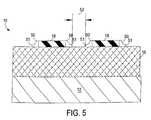
- FIG. 5is a cross-sectional view of a portion of an integrated circuit, showing an exemplary spacer with a tail in an exemplary method of manufacturing the integrated circuit illustrated in FIG. 1 .
- a cross-sectional view of a portion 10 of an integrated circuitincludes a substrate 12 , a trench line 14 , an dielectric layers 16 , patterned anti-reflective coating (ARC) features 18 , and spacers 20 .
- Portion 10is preferably part of an ultra-large-scale integrated (ULSI) circuit having millions or more transistors.
- ULSIultra-large-scale integrated
- Portion 10is manufactured as part of the IC on a semiconductor wafer, such as, a silicon wafer.
- Substrate 12is preferably single crystal silicon material or a silicided substrate, such as, Ni x Si y or Co x Si y .
- Trench line 14extends the width of dielectric layers 16 and can be filled with an electrically conductive material.
- Dielectric layers 16can include oxide, or any material with a low dielectric constant k.
- ARC features 18can be silicon nitride (Si 3 N 4 ), silicon oxynitride (SiON), or any other suitable material having appropriate anti-reflective properties.
- ARC features 18are located on top of dielectric layers 16 .
- the width between ARC features 18is preferably one minimum lithographic feature.
- Spacers 20can be any dielectric material, such as, silicon nitride, silicon oxynitride, and silicon rich nitride, and are located abutting lateral sides of ARC features 18 .
- spacers 20decrease the space or length to be etched in the creation of trench line 1 4 .
- trench line 14has a narrower width than the critical dimension possible using conventional lithographic techniques.
- trench line 14has a width of 1600 to 2500 Angstroms.
- trench line 14can have a width less than 400-1300 Angstroms.
- portion 10has a trench line with small critical dimensions.
- a cross-sectional view of portion 10illustrates photoresist features 22 , an ARC layer 28 , dielectric layers 16 , and substrate 12 .
- Photoresist features 22have been patterned with a standard feature critical dimension 25 .
- standard feature critical dimension 25is 1600 to 2500 Angstroms.
- photoresist features 22are created in a lithographic process. Photoresist features 22 are used to transfer the pattern of standard feature critical dimension 25 to ARC layer 28 .
- ARC layer 28is etched with this pattern and photoresist features 22 are stripped.
- ARC layer 28is 300 to 1000 Angstroms ( ⁇ ) thick, and dielectric layers 16 are 5,000 to 12,000 Angstroms thick.
- additional layersmay also be present in portion 10 .
- a cross-sectional view of portion 10illustrates that ARC layer 28 (FIG. 2) has been etched to form ARC features 18 .
- a thin film layer 30is deposited over ARC features 18 .
- thin film layer 30is silicon nitride (Si 3 N 4 ), silicon oxynitride (SiON), or any material suitable for the formation of spacers.
- thin film layer 30has a thickness of 100-600 Angstroms. In alternative embodiments, the thickness of thin film layer 30 varies, depending on the amount of shrinking desired. For example, thin film layer 30 may be 100 Angstroms thick to result in a contact shrink of 100 Angstroms ( ⁇ ) per side (i.e., 200 ⁇ smaller in width). The thickness of thin film layer 30 is important because it determines the spacer width. Thin film layer 30 is etched to form spacers on lateral sides of ARC features 18 .
- FIG. 4a cross-sectional view of portion 10 illustrates exemplary spacers 40 which result from the etching of thin film layer 30 (described with reference to FIG. 3 ).
- Spacers 40are formed using an etch chemistry which results in a spacer structure without a tail. Etching techniques that can be used include plasma etch and dry etch. In an exemplary embodiment, spacers 40 have a width of 100-600 Angstroms. Spacers 40 and ARC features 18 can serve as a hard mask to form a contact hole in dielectric layers 16 .
- a hard maskis a material with a high etching resistance and is used to “mask” or cover material which is intended not to be etched or removed.
- distance 42which becomes the critical dimension for the contact hole in dielectric layers 16 .
- distance 25(FIG. 2) is 1600-2500 Angstroms.
- Distance 42can be as small as 400-1300 Angstroms.
- a cross-sectional view of portion 10illustrates spacers 50 which result from the etching of thin film layer 30 (described with reference to FIG. 3 ).
- Spacers 50are formed using an etch chemistry which results in a spacer structure with a tail 51 having a convex shape.
- Etching techniques that can be usedinclude plasma etch.
- spacers 50have a width (left-to-right length) of 100-600 Angstroms ( ⁇ ).
- tail 51has a width of between 50 and 100 Angstroms ( ⁇ ). The width of tail 51 depends on etching technologies used.
- high nitride to oxide selectivity etch processcan be utilized using heavy polymer deposited dielectric gas such as CH 3 F and CH 2 F 2 .
- Spacers 50 and ARC features 18can serve as a hard mask to form a contact hole in oxide layer 16 .
- the addition of spacers 50results in a distance 52 which becomes the critical dimension for the trench line in dielectric layers 16 .
- distance 52is 1300-2200 Angstroms.
- distance 52can be as small as 200-900 Angstroms.
- trench line 14is created using spacers 20 and ARC features 18 as a hard mask.
- An etching processis used to create trench line 14 .
- a plasma etchis used.
- other etch technologiesmay be utilized.
- spacers 20can be formed as part of the hard mask, thus allowing the formation of a narrower spacing for trench line 14 .
- spacer etch chemistriescan be used to control the size of the spacer formed.
- spacers 20can be formed which include a tail.
- ARC features 18 and spacers 20results in smaller critical dimensions for trench line 14 .
- the method described with reference to FIGS. 1-5avoids the feature size limitations inherent to conventional lithography.
Landscapes
- Engineering & Computer Science (AREA)
- Physics & Mathematics (AREA)
- Condensed Matter Physics & Semiconductors (AREA)
- General Physics & Mathematics (AREA)
- Manufacturing & Machinery (AREA)
- Computer Hardware Design (AREA)
- Microelectronics & Electronic Packaging (AREA)
- Power Engineering (AREA)
- Internal Circuitry In Semiconductor Integrated Circuit Devices (AREA)
Abstract
Description
Claims (16)
Priority Applications (1)
| Application Number | Priority Date | Filing Date | Title |
|---|---|---|---|
| US09/824,415US6664180B1 (en) | 2001-04-02 | 2001-04-02 | Method of forming smaller trench line width using a spacer hard mask |
Applications Claiming Priority (1)
| Application Number | Priority Date | Filing Date | Title |
|---|---|---|---|
| US09/824,415US6664180B1 (en) | 2001-04-02 | 2001-04-02 | Method of forming smaller trench line width using a spacer hard mask |
Publications (1)
| Publication Number | Publication Date |
|---|---|
| US6664180B1true US6664180B1 (en) | 2003-12-16 |
Family
ID=29712648
Family Applications (1)
| Application Number | Title | Priority Date | Filing Date |
|---|---|---|---|
| US09/824,415Expired - LifetimeUS6664180B1 (en) | 2001-04-02 | 2001-04-02 | Method of forming smaller trench line width using a spacer hard mask |
Country Status (1)
| Country | Link |
|---|---|
| US (1) | US6664180B1 (en) |
Cited By (3)
| Publication number | Priority date | Publication date | Assignee | Title |
|---|---|---|---|---|
| US6780708B1 (en)* | 2003-03-05 | 2004-08-24 | Advanced Micro Devices, Inc. | Method of forming core and periphery gates including two critical masking steps to form a hard mask in a core region that includes a critical dimension less than achievable at a resolution limit of lithography |
| US20060145094A1 (en)* | 2004-12-30 | 2006-07-06 | Asml Netherlands B.V. | Optical element, lithographic apparatus including such an optical element, device manufacturing method, and device manufactured thereby |
| CN1324683C (en)* | 2004-07-02 | 2007-07-04 | 旺宏电子股份有限公司 | Method for forming pitches beyond the resolution of optical lithography processes |
Citations (17)
| Publication number | Priority date | Publication date | Assignee | Title |
|---|---|---|---|---|
| US5420067A (en)* | 1990-09-28 | 1995-05-30 | The United States Of America As Represented By The Secretary Of The Navy | Method of fabricatring sub-half-micron trenches and holes |
| JPH1126458A (en)* | 1997-06-30 | 1999-01-29 | Sanyo Electric Co Ltd | Semiconductor device and its manufacture |
| US5889302A (en) | 1997-04-21 | 1999-03-30 | Advanced Micro Devices, Inc. | Multilayer floating gate field effect transistor structure for use in integrated circuit devices |
| US5918132A (en) | 1996-12-31 | 1999-06-29 | Intel Corporation | Method for narrow space formation and self-aligned channel implant |
| US5923981A (en) | 1996-12-31 | 1999-07-13 | Intel Corporation | Cascading transistor gate and method for fabricating the same |
| US5936280A (en) | 1997-04-21 | 1999-08-10 | Advanced Micro Devices, Inc. | Multilayer quadruple gate field effect transistor structure for use in integrated circuit devices |
| US5942803A (en)* | 1996-03-19 | 1999-08-24 | Samsung Electronics Co., Ltd. | Methods for forming openings with improved aspect ratios in integrated circuit devices, and related structures |
| US5946566A (en) | 1996-03-01 | 1999-08-31 | Ace Memory, Inc. | Method of making a smaller geometry high capacity stacked DRAM device |
| US5989952A (en) | 1996-08-30 | 1999-11-23 | Nanya Technology Corporation | Method for fabricating a crown-type capacitor of a DRAM cell |
| US6022815A (en) | 1996-12-31 | 2000-02-08 | Intel Corporation | Method of fabricating next-to-minimum-size transistor gate using mask-edge gate definition technique |
| US6031264A (en) | 1997-09-29 | 2000-02-29 | Taiwan Semiconductor Manufacturing Company | Nitride spacer technology for flash EPROM |
| US6103605A (en) | 1999-03-17 | 2000-08-15 | National Semiconductor Corporation | Process for defining the width of silicon gates using spacers as an etch hard mask |
| US6174802B1 (en)* | 1999-06-28 | 2001-01-16 | Taiwan Semiconductor Manufacturing Company | Method for fabricating a self aligned contact which eliminates the key hole problem using a two step contact deposition |
| US6214747B1 (en) | 1999-10-28 | 2001-04-10 | United Microelectronics Corp. | Method for forming opening in a semiconductor device |
| US20010015454A1 (en)* | 1999-12-13 | 2001-08-23 | Samsung Electronics Co., Ltd | Nonvolatile semiconductor memory device and manufacturing method thereof |
| US6391753B1 (en) | 2000-06-20 | 2002-05-21 | Advanced Micro Devices, Inc. | Process for forming gate conductors |
| US20020076877A1 (en)* | 2000-06-16 | 2002-06-20 | Chartered Semiconductor Manufacturing Ltd. | Method to form self-aligned, L-shaped sidewall spacers |
- 2001
- 2001-04-02USUS09/824,415patent/US6664180B1/ennot_activeExpired - Lifetime
Patent Citations (18)
| Publication number | Priority date | Publication date | Assignee | Title |
|---|---|---|---|---|
| US5420067A (en)* | 1990-09-28 | 1995-05-30 | The United States Of America As Represented By The Secretary Of The Navy | Method of fabricatring sub-half-micron trenches and holes |
| US5946566A (en) | 1996-03-01 | 1999-08-31 | Ace Memory, Inc. | Method of making a smaller geometry high capacity stacked DRAM device |
| US5942803A (en)* | 1996-03-19 | 1999-08-24 | Samsung Electronics Co., Ltd. | Methods for forming openings with improved aspect ratios in integrated circuit devices, and related structures |
| US5989952A (en) | 1996-08-30 | 1999-11-23 | Nanya Technology Corporation | Method for fabricating a crown-type capacitor of a DRAM cell |
| US5923981A (en) | 1996-12-31 | 1999-07-13 | Intel Corporation | Cascading transistor gate and method for fabricating the same |
| US5918132A (en) | 1996-12-31 | 1999-06-29 | Intel Corporation | Method for narrow space formation and self-aligned channel implant |
| US6022815A (en) | 1996-12-31 | 2000-02-08 | Intel Corporation | Method of fabricating next-to-minimum-size transistor gate using mask-edge gate definition technique |
| US5936280A (en) | 1997-04-21 | 1999-08-10 | Advanced Micro Devices, Inc. | Multilayer quadruple gate field effect transistor structure for use in integrated circuit devices |
| US5889302A (en) | 1997-04-21 | 1999-03-30 | Advanced Micro Devices, Inc. | Multilayer floating gate field effect transistor structure for use in integrated circuit devices |
| JPH1126458A (en)* | 1997-06-30 | 1999-01-29 | Sanyo Electric Co Ltd | Semiconductor device and its manufacture |
| US6031264A (en) | 1997-09-29 | 2000-02-29 | Taiwan Semiconductor Manufacturing Company | Nitride spacer technology for flash EPROM |
| US6103605A (en) | 1999-03-17 | 2000-08-15 | National Semiconductor Corporation | Process for defining the width of silicon gates using spacers as an etch hard mask |
| US6174802B1 (en)* | 1999-06-28 | 2001-01-16 | Taiwan Semiconductor Manufacturing Company | Method for fabricating a self aligned contact which eliminates the key hole problem using a two step contact deposition |
| US6214747B1 (en) | 1999-10-28 | 2001-04-10 | United Microelectronics Corp. | Method for forming opening in a semiconductor device |
| US20010015454A1 (en)* | 1999-12-13 | 2001-08-23 | Samsung Electronics Co., Ltd | Nonvolatile semiconductor memory device and manufacturing method thereof |
| US6483146B2 (en)* | 1999-12-13 | 2002-11-19 | Samsung Electronics Co., Ltd. | Nonvolatile semiconductor memory device and manufacturing method thereof |
| US20020076877A1 (en)* | 2000-06-16 | 2002-06-20 | Chartered Semiconductor Manufacturing Ltd. | Method to form self-aligned, L-shaped sidewall spacers |
| US6391753B1 (en) | 2000-06-20 | 2002-05-21 | Advanced Micro Devices, Inc. | Process for forming gate conductors |
Non-Patent Citations (2)
| Title |
|---|
| Huang, Xuejue, et al. "Sub 50-nm Fin FET: PMOS" Department of Engineering & Computer Sciences, University of California, Berkeley, 1999 IEEE. |
| Yu, Bin, et al. "Ultra-Thin Body Silicon-On-Insulator MOSFET's for Terabit-Scale Integration" Department of Electrical Engineering & Computer Sciences, University of California, Berkeley. |
Cited By (5)
| Publication number | Priority date | Publication date | Assignee | Title |
|---|---|---|---|---|
| US6780708B1 (en)* | 2003-03-05 | 2004-08-24 | Advanced Micro Devices, Inc. | Method of forming core and periphery gates including two critical masking steps to form a hard mask in a core region that includes a critical dimension less than achievable at a resolution limit of lithography |
| US6995437B1 (en) | 2003-03-05 | 2006-02-07 | Advanced Micro Devices, Inc. | Semiconductor device with core and periphery regions |
| CN1324683C (en)* | 2004-07-02 | 2007-07-04 | 旺宏电子股份有限公司 | Method for forming pitches beyond the resolution of optical lithography processes |
| US20060145094A1 (en)* | 2004-12-30 | 2006-07-06 | Asml Netherlands B.V. | Optical element, lithographic apparatus including such an optical element, device manufacturing method, and device manufactured thereby |
| US7196343B2 (en)* | 2004-12-30 | 2007-03-27 | Asml Netherlands B.V. | Optical element, lithographic apparatus including such an optical element, device manufacturing method, and device manufactured thereby |
Similar Documents
| Publication | Publication Date | Title |
|---|---|---|
| US6514849B1 (en) | Method of forming smaller contact size using a spacer hard mask | |
| US6475867B1 (en) | Method of forming integrated circuit features by oxidation of titanium hard mask | |
| US6998332B2 (en) | Method of independent P and N gate length control of FET device made by sidewall image transfer technique | |
| US6638441B2 (en) | Method for pitch reduction | |
| US9111880B2 (en) | Method of forming a pattern in a semiconductor device and method of forming a gate using the same | |
| US6541360B1 (en) | Bi-layer trim etch process to form integrated circuit gate structures | |
| US6818141B1 (en) | Application of the CVD bilayer ARC as a hard mask for definition of the subresolution trench features between polysilicon wordlines | |
| KR970007173B1 (en) | Fine pattern formation method | |
| US6416933B1 (en) | Method to produce small space pattern using plasma polymerization layer | |
| US6514868B1 (en) | Method of creating a smaller contact using hard mask | |
| US6475811B1 (en) | System for and method of using bacteria to aid in contact hole printing | |
| KR20120126442A (en) | Method for forming pattern of Semiconductor Device | |
| US6764946B1 (en) | Method of controlling line edge roughness in resist films | |
| US6828259B2 (en) | Enhanced transistor gate using E-beam radiation | |
| US5942787A (en) | Small gate electrode MOSFET | |
| US20250285877A1 (en) | Feature patterning using pitch relaxation and directional end-pushing with ion bombardment | |
| US6329124B1 (en) | Method to produce high density memory cells and small spaces by using nitride spacer | |
| US6548423B1 (en) | Multilayer anti-reflective coating process for integrated circuit fabrication | |
| US6514867B1 (en) | Method of creating narrow trench lines using hard mask | |
| US6664180B1 (en) | Method of forming smaller trench line width using a spacer hard mask | |
| US6030752A (en) | Method of stitching segments defined by adjacent image patterns during the manufacture of a semiconductor device | |
| US6514874B1 (en) | Method of using controlled resist footing on silicon nitride substrate for smaller spacing of integrated circuit device features | |
| US6753266B1 (en) | Method of enhancing gate patterning properties with reflective hard mask | |
| KR100847369B1 (en) | Improved transistor gate using electron beam radiation and method of forming integrated circuit comprising the transistor gate | |
| US6989323B2 (en) | Method for forming narrow gate structures on sidewalls of a lithographically defined sacrificial material |
Legal Events
| Date | Code | Title | Description |
|---|---|---|---|
| AS | Assignment | Owner name:ADVANCED MICRO DEVICES, INC., CALIFORNIA Free format text:ASSIGNMENT OF ASSIGNORS INTEREST;ASSIGNORS:HUI, ANGELA T.;SINGH, BHANWAR;REEL/FRAME:011673/0216;SIGNING DATES FROM 20010309 TO 20010322 | |
| STCF | Information on status: patent grant | Free format text:PATENTED CASE | |
| FEPP | Fee payment procedure | Free format text:PAYOR NUMBER ASSIGNED (ORIGINAL EVENT CODE: ASPN); ENTITY STATUS OF PATENT OWNER: LARGE ENTITY | |
| FPAY | Fee payment | Year of fee payment:4 | |
| AS | Assignment | Owner name:GLOBALFOUNDRIES INC., CAYMAN ISLANDS Free format text:AFFIRMATION OF PATENT ASSIGNMENT;ASSIGNOR:ADVANCED MICRO DEVICES, INC.;REEL/FRAME:023119/0083 Effective date:20090630 | |
| FPAY | Fee payment | Year of fee payment:8 | |
| FPAY | Fee payment | Year of fee payment:12 | |
| AS | Assignment | Owner name:WILMINGTON TRUST, NATIONAL ASSOCIATION, DELAWARE Free format text:SECURITY AGREEMENT;ASSIGNOR:GLOBALFOUNDRIES INC.;REEL/FRAME:049490/0001 Effective date:20181127 | |
| AS | Assignment | Owner name:GLOBALFOUNDRIES U.S. INC., CALIFORNIA Free format text:ASSIGNMENT OF ASSIGNORS INTEREST;ASSIGNOR:GLOBALFOUNDRIES INC.;REEL/FRAME:054633/0001 Effective date:20201022 | |
| AS | Assignment | Owner name:GLOBALFOUNDRIES INC., CAYMAN ISLANDS Free format text:RELEASE BY SECURED PARTY;ASSIGNOR:WILMINGTON TRUST, NATIONAL ASSOCIATION;REEL/FRAME:054636/0001 Effective date:20201117 | |
| AS | Assignment | Owner name:GLOBALFOUNDRIES U.S. INC., NEW YORK Free format text:RELEASE BY SECURED PARTY;ASSIGNOR:WILMINGTON TRUST, NATIONAL ASSOCIATION;REEL/FRAME:056987/0001 Effective date:20201117 |