US6664160B2 - Gate structure with high K dielectric - Google Patents
Gate structure with high K dielectricDownload PDFInfo
- Publication number
- US6664160B2 US6664160B2US10/298,564US29856402AUS6664160B2US 6664160 B2US6664160 B2US 6664160B2US 29856402 AUS29856402 AUS 29856402AUS 6664160 B2US6664160 B2US 6664160B2
- Authority
- US
- United States
- Prior art keywords
- layer
- hfo
- semiconductor device
- gate structure
- recited
- Prior art date
- Legal status (The legal status is an assumption and is not a legal conclusion. Google has not performed a legal analysis and makes no representation as to the accuracy of the status listed.)
- Expired - Lifetime
Links
Images


Classifications
- H—ELECTRICITY
- H01—ELECTRIC ELEMENTS
- H01L—SEMICONDUCTOR DEVICES NOT COVERED BY CLASS H10
- H01L21/00—Processes or apparatus adapted for the manufacture or treatment of semiconductor or solid state devices or of parts thereof
- H01L21/02—Manufacture or treatment of semiconductor devices or of parts thereof
- H01L21/04—Manufacture or treatment of semiconductor devices or of parts thereof the devices having potential barriers, e.g. a PN junction, depletion layer or carrier concentration layer
- H01L21/18—Manufacture or treatment of semiconductor devices or of parts thereof the devices having potential barriers, e.g. a PN junction, depletion layer or carrier concentration layer the devices having semiconductor bodies comprising elements of Group IV of the Periodic Table or AIIIBV compounds with or without impurities, e.g. doping materials
- H—ELECTRICITY
- H10—SEMICONDUCTOR DEVICES; ELECTRIC SOLID-STATE DEVICES NOT OTHERWISE PROVIDED FOR
- H10D—INORGANIC ELECTRIC SEMICONDUCTOR DEVICES
- H10D64/00—Electrodes of devices having potential barriers
- H10D64/60—Electrodes characterised by their materials
- H10D64/66—Electrodes having a conductor capacitively coupled to a semiconductor by an insulator, e.g. MIS electrodes
- H10D64/68—Electrodes having a conductor capacitively coupled to a semiconductor by an insulator, e.g. MIS electrodes characterised by the insulator, e.g. by the gate insulator
- H10D64/691—Electrodes having a conductor capacitively coupled to a semiconductor by an insulator, e.g. MIS electrodes characterised by the insulator, e.g. by the gate insulator comprising metallic compounds, e.g. metal oxides or metal silicates
- C—CHEMISTRY; METALLURGY
- C23—COATING METALLIC MATERIAL; COATING MATERIAL WITH METALLIC MATERIAL; CHEMICAL SURFACE TREATMENT; DIFFUSION TREATMENT OF METALLIC MATERIAL; COATING BY VACUUM EVAPORATION, BY SPUTTERING, BY ION IMPLANTATION OR BY CHEMICAL VAPOUR DEPOSITION, IN GENERAL; INHIBITING CORROSION OF METALLIC MATERIAL OR INCRUSTATION IN GENERAL
- C23C—COATING METALLIC MATERIAL; COATING MATERIAL WITH METALLIC MATERIAL; SURFACE TREATMENT OF METALLIC MATERIAL BY DIFFUSION INTO THE SURFACE, BY CHEMICAL CONVERSION OR SUBSTITUTION; COATING BY VACUUM EVAPORATION, BY SPUTTERING, BY ION IMPLANTATION OR BY CHEMICAL VAPOUR DEPOSITION, IN GENERAL
- C23C16/00—Chemical coating by decomposition of gaseous compounds, without leaving reaction products of surface material in the coating, i.e. chemical vapour deposition [CVD] processes
- C23C16/22—Chemical coating by decomposition of gaseous compounds, without leaving reaction products of surface material in the coating, i.e. chemical vapour deposition [CVD] processes characterised by the deposition of inorganic material, other than metallic material
- C23C16/30—Deposition of compounds, mixtures or solid solutions, e.g. borides, carbides, nitrides
- C23C16/40—Oxides
- C23C16/405—Oxides of refractory metals or yttrium
- H—ELECTRICITY
- H01—ELECTRIC ELEMENTS
- H01L—SEMICONDUCTOR DEVICES NOT COVERED BY CLASS H10
- H01L21/00—Processes or apparatus adapted for the manufacture or treatment of semiconductor or solid state devices or of parts thereof
- H01L21/02—Manufacture or treatment of semiconductor devices or of parts thereof
- H01L21/02104—Forming layers
- H01L21/02107—Forming insulating materials on a substrate
- H01L21/02225—Forming insulating materials on a substrate characterised by the process for the formation of the insulating layer
- H01L21/0226—Forming insulating materials on a substrate characterised by the process for the formation of the insulating layer formation by a deposition process
- H01L21/02263—Forming insulating materials on a substrate characterised by the process for the formation of the insulating layer formation by a deposition process deposition from the gas or vapour phase
- H—ELECTRICITY
- H01—ELECTRIC ELEMENTS
- H01L—SEMICONDUCTOR DEVICES NOT COVERED BY CLASS H10
- H01L21/00—Processes or apparatus adapted for the manufacture or treatment of semiconductor or solid state devices or of parts thereof
- H01L21/02—Manufacture or treatment of semiconductor devices or of parts thereof
- H01L21/04—Manufacture or treatment of semiconductor devices or of parts thereof the devices having potential barriers, e.g. a PN junction, depletion layer or carrier concentration layer
- H01L21/18—Manufacture or treatment of semiconductor devices or of parts thereof the devices having potential barriers, e.g. a PN junction, depletion layer or carrier concentration layer the devices having semiconductor bodies comprising elements of Group IV of the Periodic Table or AIIIBV compounds with or without impurities, e.g. doping materials
- H01L21/28—Manufacture of electrodes on semiconductor bodies using processes or apparatus not provided for in groups H01L21/20 - H01L21/268
- H01L21/28008—Making conductor-insulator-semiconductor electrodes
- H01L21/28017—Making conductor-insulator-semiconductor electrodes the insulator being formed after the semiconductor body, the semiconductor being silicon
- H01L21/28158—Making the insulator
- H01L21/28167—Making the insulator on single crystalline silicon, e.g. using a liquid, i.e. chemical oxidation
- H01L21/28185—Making the insulator on single crystalline silicon, e.g. using a liquid, i.e. chemical oxidation with a treatment, e.g. annealing, after the formation of the gate insulator and before the formation of the definitive gate conductor
- H—ELECTRICITY
- H01—ELECTRIC ELEMENTS
- H01L—SEMICONDUCTOR DEVICES NOT COVERED BY CLASS H10
- H01L21/00—Processes or apparatus adapted for the manufacture or treatment of semiconductor or solid state devices or of parts thereof
- H01L21/02—Manufacture or treatment of semiconductor devices or of parts thereof
- H01L21/04—Manufacture or treatment of semiconductor devices or of parts thereof the devices having potential barriers, e.g. a PN junction, depletion layer or carrier concentration layer
- H01L21/18—Manufacture or treatment of semiconductor devices or of parts thereof the devices having potential barriers, e.g. a PN junction, depletion layer or carrier concentration layer the devices having semiconductor bodies comprising elements of Group IV of the Periodic Table or AIIIBV compounds with or without impurities, e.g. doping materials
- H01L21/28—Manufacture of electrodes on semiconductor bodies using processes or apparatus not provided for in groups H01L21/20 - H01L21/268
- H01L21/28008—Making conductor-insulator-semiconductor electrodes
- H01L21/28017—Making conductor-insulator-semiconductor electrodes the insulator being formed after the semiconductor body, the semiconductor being silicon
- H01L21/28158—Making the insulator
- H01L21/28167—Making the insulator on single crystalline silicon, e.g. using a liquid, i.e. chemical oxidation
- H01L21/28194—Making the insulator on single crystalline silicon, e.g. using a liquid, i.e. chemical oxidation by deposition, e.g. evaporation, ALD, CVD, sputtering, laser deposition
- H—ELECTRICITY
- H10—SEMICONDUCTOR DEVICES; ELECTRIC SOLID-STATE DEVICES NOT OTHERWISE PROVIDED FOR
- H10D—INORGANIC ELECTRIC SEMICONDUCTOR DEVICES
- H10D64/00—Electrodes of devices having potential barriers
- H10D64/01—Manufacture or treatment
- H10D64/017—Manufacture or treatment using dummy gates in processes wherein at least parts of the final gates are self-aligned to the dummy gates, i.e. replacement gate processes
- H—ELECTRICITY
- H01—ELECTRIC ELEMENTS
- H01L—SEMICONDUCTOR DEVICES NOT COVERED BY CLASS H10
- H01L21/00—Processes or apparatus adapted for the manufacture or treatment of semiconductor or solid state devices or of parts thereof
- H01L21/02—Manufacture or treatment of semiconductor devices or of parts thereof
- H01L21/02104—Forming layers
- H01L21/02107—Forming insulating materials on a substrate
- H01L21/02109—Forming insulating materials on a substrate characterised by the type of layer, e.g. type of material, porous/non-porous, pre-cursors, mixtures or laminates
- H01L21/02112—Forming insulating materials on a substrate characterised by the type of layer, e.g. type of material, porous/non-porous, pre-cursors, mixtures or laminates characterised by the material of the layer
- H01L21/02172—Forming insulating materials on a substrate characterised by the type of layer, e.g. type of material, porous/non-porous, pre-cursors, mixtures or laminates characterised by the material of the layer the material containing at least one metal element, e.g. metal oxides, metal nitrides, metal oxynitrides or metal carbides
- H01L21/02175—Forming insulating materials on a substrate characterised by the type of layer, e.g. type of material, porous/non-porous, pre-cursors, mixtures or laminates characterised by the material of the layer the material containing at least one metal element, e.g. metal oxides, metal nitrides, metal oxynitrides or metal carbides characterised by the metal
- H01L21/02181—Forming insulating materials on a substrate characterised by the type of layer, e.g. type of material, porous/non-porous, pre-cursors, mixtures or laminates characterised by the material of the layer the material containing at least one metal element, e.g. metal oxides, metal nitrides, metal oxynitrides or metal carbides characterised by the metal the material containing hafnium, e.g. HfO2
Definitions
- the present inventionrelates to a semiconductor device and, more particularly, to a method for manufacturing a gate structure incorporating a high K dielectric therein.
- a gate oxidetends to rapidly approach 30 ⁇ in thickness and below to increase the capacitance between a gate electrode and a channel region.
- silicon dioxideas a gate dielectric is limited at such thicknesses. Once silicon dioxide is formed to a thickness of less than 40 angstroms, direct tunneling may occur through the gate dielectric to the channel region, thereby increasing the leakage current associated with the gate electrode and the channel region, causing an increase in power consumption.
- One of these methodsis to use a high K dielectric material such as Ta 2 O 5 as the gate dielectric material to increase the capacitance between the gate and the channel.
- a poly-siliconis utilized as a gate electrode
- the use of Ta 2 O 5 for the gate dielectric materialhas a disadvantage in integrating the semiconductor device. That is, an undesired SiO 2 and TaSi 2 are formed at an interface between Ta 2 O 5 and the poly-silicon which, in turn, increases an equivalent oxide thickness.
- a barrier metalsuch as TiN is employed. However, the TiN changes a threshold voltage shift.
- an object of the present inventionto provide a gate structure incorporating therein a high K dielectric for use in a semiconductor device.
- a gate structure for use in a semiconductor devicecomprising a semiconductor substrate provided with an isolation region formed therein; a gate dielectric, made of HfO 2 , formed on the semiconductor substrate; and a gate line on the gate dielectric.
- a gate structure for use in a semiconductor devicecomprising a semiconductor substrate provided with an isolation region formed therein; a trench structure formed on the semiconductor substrate; a gate dielectric, made of HfO 2 , formed on the trench structure; and a gate line on the gate dielectric.
- a method for manufacturing a gate structure for use in a semiconductor devicecomprising the steps of a) preparing a semiconductor substrate provided with an isolation region formed therein; b) forming a dummy layer on the semiconductor substrate; c) patterning the dummy layer into a predetermined configuration; d) implanting dopants into the semiconductor substrate by using the patterned dummy layer as a mask, thereby obtaining a source and a drain; e) forming an inter-layer dielectric (ILD) on the semiconductor substrate and the patterned dummy layer; f) planarizing the ILD layer until a top surface of the patterned dummy layer is exposed; g) removing the patterned dummy layer, thereby opening a portion of semiconductor substrate; h) forming a HfO 2 layer on the exposed portion of the semiconductor substrate and the ILD layer; i) forming a conductive layer on the HfO 2 layer; and j) planarizing
- FIG. 1is a cross sectional view setting forth a gate structure in accordance with a first preferred embodiment of the present invention
- FIGS. 2A to 2 Care cross sectional views illustrating a method for the manufacture of the gate structure shown in FIG. 1;
- FIG. 3depicts a cross sectional view showing a gate structure in accordance with a second preferred embodiment of the present invention.
- FIGS. 4A to 4 Fare cross sectional views setting forth a method for the manufacture of the gate structure shown in FIG. 3 .
- FIGS. 1 to 4cross sectional views setting forth gate structures and methods for manufacturing the gate structures for use in a semiconductor device in accordance with preferred embodiments of the present invention.
- FIG. 1there is provided a cross sectional view of the inventive gate structure 100 comprising a semiconductor substrate 110 provided with an isolation region 120 for defining an active region, a gate oxide 134 and a gate electrode 142 .
- the gate oxide 134is made of a high dielectric material such as Hf 2 O.
- the isolation region 120may be formed in a structure of local oxidation of silicon (LOCOS) or in a structure of shallow trench isolation (STI).
- LOClocal oxidation of silicon
- STIshallow trench isolation
- the gate oxide layer 134has an effective thickness ranging from approximately 10 ⁇ to approximately 45 ⁇ .
- the process for manufacturing the gate structure 100begins with the preparation of a semiconductor substrate 110 including an isolation region 120 for defining an active region.
- the isolation region 120may be formed in a structure of local oxidation of silicon (LOCOS) or in a structure of shallow trench isolation (STI).
- LOCSlocal oxidation of silicon
- STIshallow trench isolation
- the semiconductor substrate 110can be cleaned by using a chemical such as a mixture of H 2 SO 4 and H 2 O 2 at a hydrogen gas atmosphere to remove an undesired silicon dioxide (SiO 2 ) formed thereon.
- the semiconductor substrate 110may be cleaned by a solution prepared by mixing ammonium hydroxide (NH 4 OH), hydrogen peroxide (H 2 O 2 ) and deionized (DI) water. It is preferable that the cleaning process be carried out at a temperature ranging from approximately 850° C. to approximately 950° C. in ultra high vacuum (UHV). An ultra thin silicon dioxide (not shown) can be formed on top of the cleaned silicon substrate 110 .
- a Hf 2 O layer 130is formed on top of the semiconductor substrate 110 by using an atomic layer deposition (ALD) method, as shown in FIG. 2 A.
- the ALD methodis carried out by dosing the precursor in the presence of a gas selected from a group consisting of N 2 gas, NH 3 gas and ND 3 gas; and purging the precursor by using a gas selected from a group consisting of N 2 gas, NH 3 gas and ND 3 gas.
- a H 2 O vaporis utilized as an oxygen source and a precursor of Hf is selected from a group consisting of Hf tert-butaoxide (Hf[OC(CH 3 )] 4 ), Hf(th)Cl 4 and HfCl 4 .
- the HfO 2 layer 130has an effective thickness (or an equivalent oxide thickness) ranging from approximately 10 ⁇ to approximately 45 ⁇ .
- the HfO 2 layer 130can be formed by using a chemical vapor deposition (CVD) method.
- the CVD methodutilizes a Hf tert-butaoxide (Hf[OC(CH 3 )] 4 ) as a precursor of Hf and a gas selected from a group consisting of O 2 , N 2 O and D 2 O as an oxygen source.
- the HfO 2 layer 130can be formed by using a plasma CVD.
- the plasma CVDutilizes an excited gas selected from a group consisting of He, Ar, Kr and Xe as a source gas.
- the plasma sourceis controlled by using a remote control in the microwave range of 1-9 GHz and a wafer is maintained at a temperature ranging from approximately 200° C.
- the HfO 2 layer 130is annealed by using a rapid thermal process (RTP) in order to improve the characteristics thereof.
- RTPrapid thermal process
- the RTPis carried out in the presence of O 2 or N 2 O at a temperature ranging from approximately 500° C. to approximately 800° C. for 10-120 seconds. It is also preferable that a ramp rate be 20-80° C./sec.
- the annealing processcan be carried out in a furnace in the presence of O 2 , N 2 , or N 2 O at a temperature ranging from approximately 450° C. to approximately 800° C. for 10-60 minutes.
- the annealing processcan also be carried out by using an UV-Ozone at a temperature ranging from approximately 300° C. to approximately 500° C. for 1-20 minutes.
- a conductive layer 140is formed on the Hf 2 O layer 130 .
- the conductive layer 140is made of a material selected from a group consisting of doped poly-Si, amorphous-Si, W-polycide, Ti-polycide, Co-polycide, W, W/WN stack, Ta, denuded WN and TaN.
- the conductive layer 140 and the Hf 2 O layer 130are patterned into the gate oxide 134 and the gate electrode 142 , as shown in FIG. 2 C.
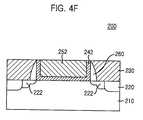
- FIG. 3there is provided a cross sectional view of a gate structure 200 in accordance with a second preferred embodiment of the present invention, comprising a semiconductor substrate 210 provided with a source/drain 222 and an isolation region 220 for defining an active region, a gate oxide 242 , a gate electrode 252 , a spacer 260 and an inter-layer dielectric (ILD) layer 230 .
- a semiconductor substrate 210provided with a source/drain 222 and an isolation region 220 for defining an active region
- a gate oxide 242for defining an active region
- a gate electrode 252for defining an active region
- spacer 260for defining an active region
- ILDinter-layer dielectric
- the gate structure 200 of the second preferred embodimentis similar to that of the first preferred embodiment except that the gate oxide 242 is formed in the form of trench. Further, the second preferred embodiment has the spacer 260 formed on sides of the gate oxide 242 .
- the process for manufacturing the gate structure 200begins with the preparation of a semiconductor substrate 210 including an isolation region 220 for defining an active region.
- the isolation region 220may be formed in a structure of local oxidation of silicon (LOCOS) or in a structure of shallow trench isolation (STI).
- LOCSlocal oxidation of silicon
- STIshallow trench isolation
- a dummy gate oxide and a dummy poly-Si, layerare formed on the semiconductor substrate 210 , sequentially.
- the dummy gate oxide and the dummy poly-Si layerare patterned into a predetermined configuration, thereby obtaining a patterned dummy gate oxide layer 204 and a patterned dummy poly-Si layer 202 .
- Dopantsare implanted into the semiconductor substrate 210 to form a source/drain 222 , wherein the patterned dummy poly-Si layer 202 is utilized as a mask.
- a spacer 260is formed around the patterned dummy gate oxide layer 204 and the patterned dummy poly-Si layer 202 is exposed.
- an ILD layer 230is formed on top of the patterned dummy poly-Si layer 202 and the semiconductor substrate 210 .
- the ILD layer 230is planarized by using a method such as a chemical mechanical polishing (CMP) until a top surface of the patterned dummy poly-Si layer 202 is exposed.
- CMPchemical mechanical polishing
- the patterned dummy gate oxide layer 204 and the patterned dummy poly-Si layer 202are removed by using a method such as a wet etching, thereby obtaining a trench 270 which exposes a portion of the semiconductor substrate 210 .
- a HfO 2 layer 240 and then a conductive layer 250are subsequently formed on the ILD layer 230 and the trench.
- the method of forming the HfO 2 layer 240is similar to that used to form the HfO 2 layer 130 .
- the conductive layer 250 and the HfO 2 layer 240are planarized until a top surface of the ILD layer 230 is exposed, thereby obtaining the gate oxide 242 and the gate electrode 252 . Finally, the remaining ILD layer 230 is removed (not shown) by using an etching process.
- an effective K of the gate dielectriccan be controlled to within 18 to 25.
- the present inventioncan obtain a high K gate dielectric with excellent leakage current characteristic as well as a low interface state with both a gate electrode and a semiconductor substrate.
Landscapes
- Engineering & Computer Science (AREA)
- Chemical & Material Sciences (AREA)
- Manufacturing & Machinery (AREA)
- General Physics & Mathematics (AREA)
- Physics & Mathematics (AREA)
- Computer Hardware Design (AREA)
- Microelectronics & Electronic Packaging (AREA)
- Power Engineering (AREA)
- Condensed Matter Physics & Semiconductors (AREA)
- Chemical Kinetics & Catalysis (AREA)
- General Chemical & Material Sciences (AREA)
- Crystallography & Structural Chemistry (AREA)
- Inorganic Chemistry (AREA)
- Materials Engineering (AREA)
- Mechanical Engineering (AREA)
- Metallurgy (AREA)
- Organic Chemistry (AREA)
- Insulated Gate Type Field-Effect Transistor (AREA)
- Formation Of Insulating Films (AREA)
Abstract
Description
Claims (17)
Priority Applications (1)
| Application Number | Priority Date | Filing Date | Title |
|---|---|---|---|
| US10/298,564US6664160B2 (en) | 2000-06-28 | 2002-11-19 | Gate structure with high K dielectric |
Applications Claiming Priority (4)
| Application Number | Priority Date | Filing Date | Title |
|---|---|---|---|
| KR2000-35965 | 2000-06-28 | ||
| KR1020000035965AKR100545706B1 (en) | 2000-06-28 | 2000-06-28 | Semiconductor device manufacturing method |
| US09/883,188US6511875B2 (en) | 2000-06-28 | 2001-06-19 | Method for making high K dielectric gate for semiconductor device |
| US10/298,564US6664160B2 (en) | 2000-06-28 | 2002-11-19 | Gate structure with high K dielectric |
Related Parent Applications (1)
| Application Number | Title | Priority Date | Filing Date |
|---|---|---|---|
| US09/883,188DivisionUS6511875B2 (en) | 2000-06-28 | 2001-06-19 | Method for making high K dielectric gate for semiconductor device |
Publications (2)
| Publication Number | Publication Date |
|---|---|
| US20030096467A1 US20030096467A1 (en) | 2003-05-22 |
| US6664160B2true US6664160B2 (en) | 2003-12-16 |
Family
ID=19674424
Family Applications (2)
| Application Number | Title | Priority Date | Filing Date |
|---|---|---|---|
| US09/883,188Expired - LifetimeUS6511875B2 (en) | 2000-06-28 | 2001-06-19 | Method for making high K dielectric gate for semiconductor device |
| US10/298,564Expired - LifetimeUS6664160B2 (en) | 2000-06-28 | 2002-11-19 | Gate structure with high K dielectric |
Family Applications Before (1)
| Application Number | Title | Priority Date | Filing Date |
|---|---|---|---|
| US09/883,188Expired - LifetimeUS6511875B2 (en) | 2000-06-28 | 2001-06-19 | Method for making high K dielectric gate for semiconductor device |
Country Status (2)
| Country | Link |
|---|---|
| US (2) | US6511875B2 (en) |
| KR (1) | KR100545706B1 (en) |
Cited By (27)
| Publication number | Priority date | Publication date | Assignee | Title |
|---|---|---|---|---|
| US20060138552A1 (en)* | 2004-09-30 | 2006-06-29 | Brask Justin K | Nonplanar transistors with metal gate electrodes |
| US7456476B2 (en) | 2003-06-27 | 2008-11-25 | Intel Corporation | Nonplanar semiconductor device with partially or fully wrapped around gate electrode and methods of fabrication |
| US7479421B2 (en) | 2005-09-28 | 2009-01-20 | Intel Corporation | Process for integrating planar and non-planar CMOS transistors on a bulk substrate and article made thereby |
| US7518196B2 (en) | 2005-02-23 | 2009-04-14 | Intel Corporation | Field effect transistor with narrow bandgap source and drain regions and method of fabrication |
| US7547637B2 (en) | 2005-06-21 | 2009-06-16 | Intel Corporation | Methods for patterning a semiconductor film |
| US7569501B2 (en) | 2002-06-14 | 2009-08-04 | Applied Materials, Inc. | ALD metal oxide deposition process using direct oxidation |
| US7579280B2 (en) | 2004-06-01 | 2009-08-25 | Intel Corporation | Method of patterning a film |
| US7645710B2 (en) | 2006-03-09 | 2010-01-12 | Applied Materials, Inc. | Method and apparatus for fabricating a high dielectric constant transistor gate using a low energy plasma system |
| US7678710B2 (en) | 2006-03-09 | 2010-03-16 | Applied Materials, Inc. | Method and apparatus for fabricating a high dielectric constant transistor gate using a low energy plasma system |
| US7714397B2 (en) | 2003-06-27 | 2010-05-11 | Intel Corporation | Tri-gate transistor device with stress incorporation layer and method of fabrication |
| US7736956B2 (en) | 2005-08-17 | 2010-06-15 | Intel Corporation | Lateral undercut of metal gate in SOI device |
| US7781771B2 (en) | 2004-03-31 | 2010-08-24 | Intel Corporation | Bulk non-planar transistor having strained enhanced mobility and methods of fabrication |
| US7837838B2 (en) | 2006-03-09 | 2010-11-23 | Applied Materials, Inc. | Method of fabricating a high dielectric constant transistor gate using a low energy plasma apparatus |
| US7879675B2 (en) | 2005-03-14 | 2011-02-01 | Intel Corporation | Field effect transistor with metal source/drain regions |
| US7898041B2 (en) | 2005-06-30 | 2011-03-01 | Intel Corporation | Block contact architectures for nanoscale channel transistors |
| US7902018B2 (en) | 2006-09-26 | 2011-03-08 | Applied Materials, Inc. | Fluorine plasma treatment of high-k gate stack for defect passivation |
| US7902014B2 (en) | 2005-09-28 | 2011-03-08 | Intel Corporation | CMOS devices with a single work function gate electrode and method of fabrication |
| US7915167B2 (en) | 2004-09-29 | 2011-03-29 | Intel Corporation | Fabrication of channel wraparound gate structure for field-effect transistor |
| US7960794B2 (en) | 2004-08-10 | 2011-06-14 | Intel Corporation | Non-planar pMOS structure with a strained channel region and an integrated strained CMOS flow |
| US7989280B2 (en) | 2005-11-30 | 2011-08-02 | Intel Corporation | Dielectric interface for group III-V semiconductor device |
| US8067818B2 (en) | 2004-10-25 | 2011-11-29 | Intel Corporation | Nonplanar device with thinned lower body portion and method of fabrication |
| US8084818B2 (en) | 2004-06-30 | 2011-12-27 | Intel Corporation | High mobility tri-gate devices and methods of fabrication |
| US8119210B2 (en) | 2004-05-21 | 2012-02-21 | Applied Materials, Inc. | Formation of a silicon oxynitride layer on a high-k dielectric material |
| US8268709B2 (en) | 2004-09-29 | 2012-09-18 | Intel Corporation | Independently accessed double-gate and tri-gate transistors in same process flow |
| US8362566B2 (en) | 2008-06-23 | 2013-01-29 | Intel Corporation | Stress in trigate devices using complimentary gate fill materials |
| US8617945B2 (en) | 2006-08-02 | 2013-12-31 | Intel Corporation | Stacking fault and twin blocking barrier for integrating III-V on Si |
| US9337307B2 (en) | 2005-06-15 | 2016-05-10 | Intel Corporation | Method for fabricating transistor with thinned channel |
Families Citing this family (38)
| Publication number | Priority date | Publication date | Assignee | Title |
|---|---|---|---|---|
| US6620723B1 (en) | 2000-06-27 | 2003-09-16 | Applied Materials, Inc. | Formation of boride barrier layers using chemisorption techniques |
| KR100693781B1 (en)* | 2000-10-25 | 2007-03-12 | 주식회사 하이닉스반도체 | Silicate Forming Method Using Monoatomic Layer Deposition |
| KR100379621B1 (en)* | 2001-07-10 | 2003-04-10 | 광주과학기술원 | Gate insulator of MOS transistor and method for fabricating the same |
| US6720027B2 (en)* | 2002-04-08 | 2004-04-13 | Applied Materials, Inc. | Cyclical deposition of a variable content titanium silicon nitride layer |
| US6846516B2 (en)* | 2002-04-08 | 2005-01-25 | Applied Materials, Inc. | Multiple precursor cyclical deposition system |
| US20030235961A1 (en)* | 2002-04-17 | 2003-12-25 | Applied Materials, Inc. | Cyclical sequential deposition of multicomponent films |
| US20030232501A1 (en)* | 2002-06-14 | 2003-12-18 | Kher Shreyas S. | Surface pre-treatment for enhancement of nucleation of high dielectric constant materials |
| US6858547B2 (en)* | 2002-06-14 | 2005-02-22 | Applied Materials, Inc. | System and method for forming a gate dielectric |
| KR100513719B1 (en) | 2002-08-12 | 2005-09-07 | 삼성전자주식회사 | Precursor for the hafnium oxide film and process for preparing the hafnium oxide film by the precursor |
| KR100945648B1 (en)* | 2002-10-29 | 2010-03-04 | 매그나칩 반도체 유한회사 | Transistor of semiconductor device and manufacturing method thereof |
| US7262133B2 (en) | 2003-01-07 | 2007-08-28 | Applied Materials, Inc. | Enhancement of copper line reliability using thin ALD tan film to cap the copper line |
| CN1320606C (en)* | 2003-03-04 | 2007-06-06 | 台湾积体电路制造股份有限公司 | A gate dielectric layer and method for improving its electrical properties |
| US20040198069A1 (en) | 2003-04-04 | 2004-10-07 | Applied Materials, Inc. | Method for hafnium nitride deposition |
| TW200526804A (en)* | 2003-10-30 | 2005-08-16 | Tokyo Electron Ltd | Method of manufacturing semiconductor device, film-forming apparatus, and storage medium |
| KR100575092B1 (en) | 2003-12-24 | 2006-05-03 | 한국전자통신연구원 | Method of forming gate insulating film |
| KR100564801B1 (en)* | 2003-12-30 | 2006-03-28 | 동부아남반도체 주식회사 | Semiconductor manufacturing method |
| KR100538444B1 (en)* | 2003-12-31 | 2005-12-22 | 동부아남반도체 주식회사 | Method for fabricating via hole and trench |
| US7037816B2 (en)* | 2004-01-23 | 2006-05-02 | Taiwan Semiconductor Manufacturing Company, Ltd. | System and method for integration of HfO2 and RTCVD poly-silicon |
| US20050252449A1 (en) | 2004-05-12 | 2005-11-17 | Nguyen Son T | Control of gas flow and delivery to suppress the formation of particles in an MOCVD/ALD system |
| US20060062917A1 (en)* | 2004-05-21 | 2006-03-23 | Shankar Muthukrishnan | Vapor deposition of hafnium silicate materials with tris(dimethylamino)silane |
| US20060019033A1 (en)* | 2004-05-21 | 2006-01-26 | Applied Materials, Inc. | Plasma treatment of hafnium-containing materials |
| US20060153995A1 (en)* | 2004-05-21 | 2006-07-13 | Applied Materials, Inc. | Method for fabricating a dielectric stack |
| US8323754B2 (en)* | 2004-05-21 | 2012-12-04 | Applied Materials, Inc. | Stabilization of high-k dielectric materials |
| US20070020890A1 (en)* | 2005-07-19 | 2007-01-25 | Applied Materials, Inc. | Method and apparatus for semiconductor processing |
| US20070049043A1 (en)* | 2005-08-23 | 2007-03-01 | Applied Materials, Inc. | Nitrogen profile engineering in HI-K nitridation for device performance enhancement and reliability improvement |
| US7402534B2 (en)* | 2005-08-26 | 2008-07-22 | Applied Materials, Inc. | Pretreatment processes within a batch ALD reactor |
| US20070065578A1 (en)* | 2005-09-21 | 2007-03-22 | Applied Materials, Inc. | Treatment processes for a batch ALD reactor |
| KR100654554B1 (en)* | 2005-12-29 | 2006-12-05 | 동부일렉트로닉스 주식회사 | Manufacturing method of semiconductor device |
| US7964514B2 (en)* | 2006-03-02 | 2011-06-21 | Applied Materials, Inc. | Multiple nitrogen plasma treatments for thin SiON dielectrics |
| US20070252299A1 (en)* | 2006-04-27 | 2007-11-01 | Applied Materials, Inc. | Synchronization of precursor pulsing and wafer rotation |
| US7798096B2 (en)* | 2006-05-05 | 2010-09-21 | Applied Materials, Inc. | Plasma, UV and ion/neutral assisted ALD or CVD in a batch tool |
| US20070259111A1 (en)* | 2006-05-05 | 2007-11-08 | Singh Kaushal K | Method and apparatus for photo-excitation of chemicals for atomic layer deposition of dielectric film |
| US7659158B2 (en) | 2008-03-31 | 2010-02-09 | Applied Materials, Inc. | Atomic layer deposition processes for non-volatile memory devices |
| US20100062149A1 (en) | 2008-09-08 | 2010-03-11 | Applied Materials, Inc. | Method for tuning a deposition rate during an atomic layer deposition process |
| US8491967B2 (en)* | 2008-09-08 | 2013-07-23 | Applied Materials, Inc. | In-situ chamber treatment and deposition process |
| US9529265B2 (en) | 2014-05-05 | 2016-12-27 | Taiwan Semiconductor Manufacturing Company, Ltd. | Method of preparing and using photosensitive material |
| JP7562709B2 (en)* | 2020-06-17 | 2024-10-07 | アプライド マテリアルズ インコーポレイテッド | Gate interface engineering with doped layers |
| US20240194479A1 (en)* | 2021-04-22 | 2024-06-13 | Applied Materials, Inc. | Methods and applications of novel amorphous high-k metal-oxide dielectrics by super-cycle atomic layer deposition |
Citations (9)
| Publication number | Priority date | Publication date | Assignee | Title |
|---|---|---|---|---|
| US6013553A (en)* | 1997-07-24 | 2000-01-11 | Texas Instruments Incorporated | Zirconium and/or hafnium oxynitride gate dielectric |
| US6020024A (en)* | 1997-08-04 | 2000-02-01 | Motorola, Inc. | Method for forming high dielectric constant metal oxides |
| US6087231A (en)* | 1999-08-05 | 2000-07-11 | Advanced Micro Devices, Inc. | Fabrication of dual gates of field transistors with prevention of reaction between the gate electrode and the gate dielectric with a high dielectric constant |
| US6096590A (en)* | 1996-07-18 | 2000-08-01 | International Business Machines Corporation | Scalable MOS field effect transistor |
| US6200866B1 (en)* | 1998-02-23 | 2001-03-13 | Sharp Laboratories Of America, Inc. | Use of silicon germanium and other alloys as the replacement gate for the fabrication of MOSFET |
| US6207589B1 (en)* | 1999-07-19 | 2001-03-27 | Sharp Laboratories Of America, Inc. | Method of forming a doped metal oxide dielectric film |
| US6221712B1 (en)* | 1999-08-30 | 2001-04-24 | United Microelectronics Corp. | Method for fabricating gate oxide layer |
| US6320784B1 (en)* | 2000-03-14 | 2001-11-20 | Motorola, Inc. | Memory cell and method for programming thereof |
| US6376888B1 (en)* | 1999-04-30 | 2002-04-23 | Kabushiki Kaisha Toshiba | Semiconductor device and method of manufacturing the same |
Family Cites Families (2)
| Publication number | Priority date | Publication date | Assignee | Title |
|---|---|---|---|---|
| KR100329282B1 (en)* | 1999-10-27 | 2002-03-18 | 김효근 | Fabrication method for gate insulating layer having high dielectric constant |
| KR100368311B1 (en)* | 2000-06-27 | 2003-01-24 | 주식회사 하이닉스반도체 | Method of forming a gate in a semiconductor device |
- 2000
- 2000-06-28KRKR1020000035965Apatent/KR100545706B1/ennot_activeExpired - Lifetime
- 2001
- 2001-06-19USUS09/883,188patent/US6511875B2/ennot_activeExpired - Lifetime
- 2002
- 2002-11-19USUS10/298,564patent/US6664160B2/ennot_activeExpired - Lifetime
Patent Citations (9)
| Publication number | Priority date | Publication date | Assignee | Title |
|---|---|---|---|---|
| US6096590A (en)* | 1996-07-18 | 2000-08-01 | International Business Machines Corporation | Scalable MOS field effect transistor |
| US6013553A (en)* | 1997-07-24 | 2000-01-11 | Texas Instruments Incorporated | Zirconium and/or hafnium oxynitride gate dielectric |
| US6020024A (en)* | 1997-08-04 | 2000-02-01 | Motorola, Inc. | Method for forming high dielectric constant metal oxides |
| US6200866B1 (en)* | 1998-02-23 | 2001-03-13 | Sharp Laboratories Of America, Inc. | Use of silicon germanium and other alloys as the replacement gate for the fabrication of MOSFET |
| US6376888B1 (en)* | 1999-04-30 | 2002-04-23 | Kabushiki Kaisha Toshiba | Semiconductor device and method of manufacturing the same |
| US6207589B1 (en)* | 1999-07-19 | 2001-03-27 | Sharp Laboratories Of America, Inc. | Method of forming a doped metal oxide dielectric film |
| US6087231A (en)* | 1999-08-05 | 2000-07-11 | Advanced Micro Devices, Inc. | Fabrication of dual gates of field transistors with prevention of reaction between the gate electrode and the gate dielectric with a high dielectric constant |
| US6221712B1 (en)* | 1999-08-30 | 2001-04-24 | United Microelectronics Corp. | Method for fabricating gate oxide layer |
| US6320784B1 (en)* | 2000-03-14 | 2001-11-20 | Motorola, Inc. | Memory cell and method for programming thereof |
Non-Patent Citations (1)
| Title |
|---|
| US patent application Paper US 2001/00533601 A1 By Mogami.* |
Cited By (60)
| Publication number | Priority date | Publication date | Assignee | Title |
|---|---|---|---|---|
| US7569501B2 (en) | 2002-06-14 | 2009-08-04 | Applied Materials, Inc. | ALD metal oxide deposition process using direct oxidation |
| US7569500B2 (en) | 2002-06-14 | 2009-08-04 | Applied Materials, Inc. | ALD metal oxide deposition process using direct oxidation |
| US7714397B2 (en) | 2003-06-27 | 2010-05-11 | Intel Corporation | Tri-gate transistor device with stress incorporation layer and method of fabrication |
| US7456476B2 (en) | 2003-06-27 | 2008-11-25 | Intel Corporation | Nonplanar semiconductor device with partially or fully wrapped around gate electrode and methods of fabrication |
| US8273626B2 (en) | 2003-06-27 | 2012-09-25 | Intel Corporationn | Nonplanar semiconductor device with partially or fully wrapped around gate electrode and methods of fabrication |
| US7820513B2 (en) | 2003-06-27 | 2010-10-26 | Intel Corporation | Nonplanar semiconductor device with partially or fully wrapped around gate electrode and methods of fabrication |
| US8405164B2 (en) | 2003-06-27 | 2013-03-26 | Intel Corporation | Tri-gate transistor device with stress incorporation layer and method of fabrication |
| US7781771B2 (en) | 2004-03-31 | 2010-08-24 | Intel Corporation | Bulk non-planar transistor having strained enhanced mobility and methods of fabrication |
| US8119210B2 (en) | 2004-05-21 | 2012-02-21 | Applied Materials, Inc. | Formation of a silicon oxynitride layer on a high-k dielectric material |
| US7579280B2 (en) | 2004-06-01 | 2009-08-25 | Intel Corporation | Method of patterning a film |
| US8084818B2 (en) | 2004-06-30 | 2011-12-27 | Intel Corporation | High mobility tri-gate devices and methods of fabrication |
| US7960794B2 (en) | 2004-08-10 | 2011-06-14 | Intel Corporation | Non-planar pMOS structure with a strained channel region and an integrated strained CMOS flow |
| US8268709B2 (en) | 2004-09-29 | 2012-09-18 | Intel Corporation | Independently accessed double-gate and tri-gate transistors in same process flow |
| US8399922B2 (en) | 2004-09-29 | 2013-03-19 | Intel Corporation | Independently accessed double-gate and tri-gate transistors |
| US7915167B2 (en) | 2004-09-29 | 2011-03-29 | Intel Corporation | Fabrication of channel wraparound gate structure for field-effect transistor |
| US7531437B2 (en)* | 2004-09-30 | 2009-05-12 | Intel Corporation | Method of forming metal gate electrodes using sacrificial gate electrode material and sacrificial gate dielectric material |
| US7528025B2 (en) | 2004-09-30 | 2009-05-05 | Intel Corporation | Nonplanar transistors with metal gate electrodes |
| US20060138552A1 (en)* | 2004-09-30 | 2006-06-29 | Brask Justin K | Nonplanar transistors with metal gate electrodes |
| US8502351B2 (en) | 2004-10-25 | 2013-08-06 | Intel Corporation | Nonplanar device with thinned lower body portion and method of fabrication |
| US8749026B2 (en) | 2004-10-25 | 2014-06-10 | Intel Corporation | Nonplanar device with thinned lower body portion and method of fabrication |
| US9190518B2 (en) | 2004-10-25 | 2015-11-17 | Intel Corporation | Nonplanar device with thinned lower body portion and method of fabrication |
| US9741809B2 (en) | 2004-10-25 | 2017-08-22 | Intel Corporation | Nonplanar device with thinned lower body portion and method of fabrication |
| US10236356B2 (en) | 2004-10-25 | 2019-03-19 | Intel Corporation | Nonplanar device with thinned lower body portion and method of fabrication |
| US8067818B2 (en) | 2004-10-25 | 2011-11-29 | Intel Corporation | Nonplanar device with thinned lower body portion and method of fabrication |
| US8183646B2 (en) | 2005-02-23 | 2012-05-22 | Intel Corporation | Field effect transistor with narrow bandgap source and drain regions and method of fabrication |
| US7825481B2 (en) | 2005-02-23 | 2010-11-02 | Intel Corporation | Field effect transistor with narrow bandgap source and drain regions and method of fabrication |
| US9368583B2 (en) | 2005-02-23 | 2016-06-14 | Intel Corporation | Field effect transistor with narrow bandgap source and drain regions and method of fabrication |
| US9048314B2 (en) | 2005-02-23 | 2015-06-02 | Intel Corporation | Field effect transistor with narrow bandgap source and drain regions and method of fabrication |
| US7893506B2 (en) | 2005-02-23 | 2011-02-22 | Intel Corporation | Field effect transistor with narrow bandgap source and drain regions and method of fabrication |
| US7518196B2 (en) | 2005-02-23 | 2009-04-14 | Intel Corporation | Field effect transistor with narrow bandgap source and drain regions and method of fabrication |
| US8816394B2 (en) | 2005-02-23 | 2014-08-26 | Intel Corporation | Field effect transistor with narrow bandgap source and drain regions and method of fabrication |
| US8664694B2 (en) | 2005-02-23 | 2014-03-04 | Intel Corporation | Field effect transistor with narrow bandgap source and drain regions and method of fabrication |
| US8368135B2 (en) | 2005-02-23 | 2013-02-05 | Intel Corporation | Field effect transistor with narrow bandgap source and drain regions and method of fabrication |
| US7879675B2 (en) | 2005-03-14 | 2011-02-01 | Intel Corporation | Field effect transistor with metal source/drain regions |
| US9337307B2 (en) | 2005-06-15 | 2016-05-10 | Intel Corporation | Method for fabricating transistor with thinned channel |
| US11978799B2 (en) | 2005-06-15 | 2024-05-07 | Tahoe Research, Ltd. | Method for fabricating transistor with thinned channel |
| US9806195B2 (en) | 2005-06-15 | 2017-10-31 | Intel Corporation | Method for fabricating transistor with thinned channel |
| US8933458B2 (en) | 2005-06-21 | 2015-01-13 | Intel Corporation | Semiconductor device structures and methods of forming semiconductor structures |
| US9761724B2 (en) | 2005-06-21 | 2017-09-12 | Intel Corporation | Semiconductor device structures and methods of forming semiconductor structures |
| US9385180B2 (en) | 2005-06-21 | 2016-07-05 | Intel Corporation | Semiconductor device structures and methods of forming semiconductor structures |
| US8581258B2 (en) | 2005-06-21 | 2013-11-12 | Intel Corporation | Semiconductor device structures and methods of forming semiconductor structures |
| US8071983B2 (en) | 2005-06-21 | 2011-12-06 | Intel Corporation | Semiconductor device structures and methods of forming semiconductor structures |
| US7547637B2 (en) | 2005-06-21 | 2009-06-16 | Intel Corporation | Methods for patterning a semiconductor film |
| US7898041B2 (en) | 2005-06-30 | 2011-03-01 | Intel Corporation | Block contact architectures for nanoscale channel transistors |
| US7736956B2 (en) | 2005-08-17 | 2010-06-15 | Intel Corporation | Lateral undercut of metal gate in SOI device |
| US7479421B2 (en) | 2005-09-28 | 2009-01-20 | Intel Corporation | Process for integrating planar and non-planar CMOS transistors on a bulk substrate and article made thereby |
| US8294180B2 (en) | 2005-09-28 | 2012-10-23 | Intel Corporation | CMOS devices with a single work function gate electrode and method of fabrication |
| US7902014B2 (en) | 2005-09-28 | 2011-03-08 | Intel Corporation | CMOS devices with a single work function gate electrode and method of fabrication |
| US8193567B2 (en) | 2005-09-28 | 2012-06-05 | Intel Corporation | Process for integrating planar and non-planar CMOS transistors on a bulk substrate and article made thereby |
| US7989280B2 (en) | 2005-11-30 | 2011-08-02 | Intel Corporation | Dielectric interface for group III-V semiconductor device |
| US7837838B2 (en) | 2006-03-09 | 2010-11-23 | Applied Materials, Inc. | Method of fabricating a high dielectric constant transistor gate using a low energy plasma apparatus |
| US7645710B2 (en) | 2006-03-09 | 2010-01-12 | Applied Materials, Inc. | Method and apparatus for fabricating a high dielectric constant transistor gate using a low energy plasma system |
| US7678710B2 (en) | 2006-03-09 | 2010-03-16 | Applied Materials, Inc. | Method and apparatus for fabricating a high dielectric constant transistor gate using a low energy plasma system |
| US8617945B2 (en) | 2006-08-02 | 2013-12-31 | Intel Corporation | Stacking fault and twin blocking barrier for integrating III-V on Si |
| US7902018B2 (en) | 2006-09-26 | 2011-03-08 | Applied Materials, Inc. | Fluorine plasma treatment of high-k gate stack for defect passivation |
| US9450092B2 (en) | 2008-06-23 | 2016-09-20 | Intel Corporation | Stress in trigate devices using complimentary gate fill materials |
| US9224754B2 (en) | 2008-06-23 | 2015-12-29 | Intel Corporation | Stress in trigate devices using complimentary gate fill materials |
| US8741733B2 (en) | 2008-06-23 | 2014-06-03 | Intel Corporation | Stress in trigate devices using complimentary gate fill materials |
| US9806193B2 (en) | 2008-06-23 | 2017-10-31 | Intel Corporation | Stress in trigate devices using complimentary gate fill materials |
| US8362566B2 (en) | 2008-06-23 | 2013-01-29 | Intel Corporation | Stress in trigate devices using complimentary gate fill materials |
Also Published As
| Publication number | Publication date |
|---|---|
| KR20020001337A (en) | 2002-01-09 |
| US20030096467A1 (en) | 2003-05-22 |
| KR100545706B1 (en) | 2006-01-24 |
| US20020008297A1 (en) | 2002-01-24 |
| US6511875B2 (en) | 2003-01-28 |
Similar Documents
| Publication | Publication Date | Title |
|---|---|---|
| US6664160B2 (en) | Gate structure with high K dielectric | |
| TWI779063B (en) | Semiconductor structure and method for manufacturing the same | |
| US6797599B2 (en) | Gate structure and method | |
| US7785958B2 (en) | Method for making a semiconductor device having a high-k gate dielectric layer and a metal gate electrode | |
| TWI326896B (en) | Amorphous carbon etch stop layer for contact hole etch process | |
| EP1719163B1 (en) | Replacement gate flow facilitating high yield and incorporation of etch stop layers and/or stressed films | |
| US7012027B2 (en) | Zirconium oxide and hafnium oxide etching using halogen containing chemicals | |
| CN1992275B (en) | High performance circuit with metal and polysilicon gate electrode and method of manufacturing the same | |
| JP3600476B2 (en) | Method for manufacturing semiconductor device | |
| US20010029092A1 (en) | Method for forming aluminum oxide as a gate dielectric | |
| JP2004134753A (en) | Method of forming a gate insulator layer having multiple dielectric constants and multiple thicknesses | |
| JP2001267565A (en) | Method for forming a MOSFET device | |
| US6524918B2 (en) | Method for manufacturing a gate structure incorporating therein aluminum oxide as a gate dielectric | |
| CN112864009B (en) | Method for manufacturing semiconductor device, high-K dielectric structure and method for manufacturing high-K dielectric structure | |
| US8241974B2 (en) | Nonvolatile memory device with multiple blocking layers and method of fabricating the same | |
| US6261973B1 (en) | Remote plasma nitridation to allow selectively etching of oxide | |
| JP4239188B2 (en) | Method for manufacturing MOSFET element | |
| US6440868B1 (en) | Metal gate with CVD amorphous silicon layer and silicide for CMOS devices and method of making with a replacement gate process | |
| US8163626B2 (en) | Enhancing NAND flash floating gate performance | |
| CN105097534B (en) | A method of making semiconductor devices | |
| US6355548B1 (en) | Method for manufacturing a gate structure incorporated therein a high K dielectric | |
| CN104851802B (en) | A kind of semiconductor devices and preparation method thereof | |
| JP3833956B2 (en) | Semiconductor device manufacturing method and semiconductor device | |
| CN119447024B (en) | Preparation method of semiconductor structure | |
| JP2002324901A (en) | Field effect type semiconductor device and manufacturing method thereof |
Legal Events
| Date | Code | Title | Description |
|---|---|---|---|
| STCF | Information on status: patent grant | Free format text:PATENTED CASE | |
| FEPP | Fee payment procedure | Free format text:PAYOR NUMBER ASSIGNED (ORIGINAL EVENT CODE: ASPN); ENTITY STATUS OF PATENT OWNER: LARGE ENTITY | |
| FPAY | Fee payment | Year of fee payment:4 | |
| FEPP | Fee payment procedure | Free format text:PAYER NUMBER DE-ASSIGNED (ORIGINAL EVENT CODE: RMPN); ENTITY STATUS OF PATENT OWNER: LARGE ENTITY Free format text:PAYOR NUMBER ASSIGNED (ORIGINAL EVENT CODE: ASPN); ENTITY STATUS OF PATENT OWNER: LARGE ENTITY | |
| FPAY | Fee payment | Year of fee payment:8 | |
| AS | Assignment | Owner name:HYNIX SEMICONDUCTOR INC., KOREA, REPUBLIC OF Free format text:CHANGE OF NAME;ASSIGNOR:HYUNDAI ELECTRONICS INDUSTRIES CO., LTD.;REEL/FRAME:026828/0688 Effective date:20010329 | |
| AS | Assignment | Owner name:658868 N.B. INC., CANADA Free format text:ASSIGNMENT OF ASSIGNORS INTEREST;ASSIGNOR:HYNIX SEMICONDUCTOR INC.;REEL/FRAME:027231/0292 Effective date:20110822 | |
| AS | Assignment | Owner name:ROYAL BANK OF CANADA, CANADA Free format text:U.S. INTELLECTUAL PROPERTY SECURITY AGREEMENT (FOR NON-U.S. GRANTORS) - SHORT FORM;ASSIGNORS:658276 N.B. LTD.;658868 N.B. INC.;MOSAID TECHNOLOGIES INCORPORATED;REEL/FRAME:027512/0196 Effective date:20111223 | |
| AS | Assignment | Owner name:CONVERSANT IP N.B. 868 INC., CANADA Free format text:CHANGE OF NAME;ASSIGNOR:658868 N.B. INC.;REEL/FRAME:032439/0547 Effective date:20140101 | |
| AS | Assignment | Owner name:CONVERSANT IP N.B. 868 INC., CANADA Free format text:RELEASE OF SECURITY INTEREST;ASSIGNOR:ROYAL BANK OF CANADA;REEL/FRAME:033484/0344 Effective date:20140611 Owner name:CONVERSANT INTELLECTUAL PROPERTY MANAGEMENT INC., Free format text:RELEASE OF SECURITY INTEREST;ASSIGNOR:ROYAL BANK OF CANADA;REEL/FRAME:033484/0344 Effective date:20140611 Owner name:CONVERSANT IP N.B. 276 INC., CANADA Free format text:RELEASE OF SECURITY INTEREST;ASSIGNOR:ROYAL BANK OF CANADA;REEL/FRAME:033484/0344 Effective date:20140611 | |
| AS | Assignment | Owner name:ROYAL BANK OF CANADA, AS LENDER, CANADA Free format text:U.S. PATENT SECURITY AGREEMENT (FOR NON-U.S. GRANTORS);ASSIGNOR:CONVERSANT IP N.B. 868 INC.;REEL/FRAME:033707/0001 Effective date:20140611 Owner name:CPPIB CREDIT INVESTMENTS INC., AS LENDER, CANADA Free format text:U.S. PATENT SECURITY AGREEMENT (FOR NON-U.S. GRANTORS);ASSIGNOR:CONVERSANT IP N.B. 868 INC.;REEL/FRAME:033707/0001 Effective date:20140611 | |
| FPAY | Fee payment | Year of fee payment:12 | |
| AS | Assignment | Owner name:CONVERSANT INTELLECTUAL PROPERTY MANAGEMENT INC., Free format text:ASSIGNMENT OF ASSIGNORS INTEREST;ASSIGNOR:CONVERSANT IP N.B. 868 INC.;REEL/FRAME:036159/0386 Effective date:20150514 | |
| AS | Assignment | Owner name:CPPIB CREDIT INVESTMENTS, INC., CANADA Free format text:AMENDED AND RESTATED U.S. PATENT SECURITY AGREEMENT (FOR NON-U.S. GRANTORS);ASSIGNOR:CONVERSANT INTELLECTUAL PROPERTY MANAGEMENT INC.;REEL/FRAME:046900/0136 Effective date:20180731 | |
| AS | Assignment | Owner name:CONVERSANT INTELLECTUAL PROPERTY MANAGEMENT INC., CANADA Free format text:RELEASE OF U.S. PATENT AGREEMENT (FOR NON-U.S. GRANTORS);ASSIGNOR:ROYAL BANK OF CANADA, AS LENDER;REEL/FRAME:047645/0424 Effective date:20180731 Owner name:CONVERSANT INTELLECTUAL PROPERTY MANAGEMENT INC., Free format text:RELEASE OF U.S. PATENT AGREEMENT (FOR NON-U.S. GRANTORS);ASSIGNOR:ROYAL BANK OF CANADA, AS LENDER;REEL/FRAME:047645/0424 Effective date:20180731 | |
| AS | Assignment | Owner name:CONVERSANT INTELLECTUAL PROPERTY MANAGEMENT INC., CANADA Free format text:RELEASE BY SECURED PARTY;ASSIGNOR:CPPIB CREDIT INVESTMENTS INC.;REEL/FRAME:054371/0684 Effective date:20201028 |