US6664129B2 - Integrated circuits and methods for their fabrication - Google Patents
Integrated circuits and methods for their fabricationDownload PDFInfo
- Publication number
- US6664129B2 US6664129B2US10/318,833US31883302AUS6664129B2US 6664129 B2US6664129 B2US 6664129B2US 31883302 AUS31883302 AUS 31883302AUS 6664129 B2US6664129 B2US 6664129B2
- Authority
- US
- United States
- Prior art keywords
- dielectric
- substrate
- conductor
- openings
- conductive layer
- Prior art date
- Legal status (The legal status is an assumption and is not a legal conclusion. Google has not performed a legal analysis and makes no representation as to the accuracy of the status listed.)
- Expired - Lifetime
Links
Images


Classifications
- H—ELECTRICITY
- H01—ELECTRIC ELEMENTS
- H01L—SEMICONDUCTOR DEVICES NOT COVERED BY CLASS H10
- H01L21/00—Processes or apparatus adapted for the manufacture or treatment of semiconductor or solid state devices or of parts thereof
- H01L21/02—Manufacture or treatment of semiconductor devices or of parts thereof
- H01L21/04—Manufacture or treatment of semiconductor devices or of parts thereof the devices having potential barriers, e.g. a PN junction, depletion layer or carrier concentration layer
- H01L21/34—Manufacture or treatment of semiconductor devices or of parts thereof the devices having potential barriers, e.g. a PN junction, depletion layer or carrier concentration layer the devices having semiconductor bodies not provided for in groups H01L21/18, H10D48/04 and H10D48/07, with or without impurities, e.g. doping materials
- H01L21/44—Manufacture of electrodes on semiconductor bodies using processes or apparatus not provided for in groups H01L21/38 - H01L21/428
- H01L21/441—Deposition of conductive or insulating materials for electrodes
- H—ELECTRICITY
- H01—ELECTRIC ELEMENTS
- H01L—SEMICONDUCTOR DEVICES NOT COVERED BY CLASS H10
- H01L21/00—Processes or apparatus adapted for the manufacture or treatment of semiconductor or solid state devices or of parts thereof
- H01L21/70—Manufacture or treatment of devices consisting of a plurality of solid state components formed in or on a common substrate or of parts thereof; Manufacture of integrated circuit devices or of parts thereof
- H01L21/71—Manufacture of specific parts of devices defined in group H01L21/70
- H01L21/768—Applying interconnections to be used for carrying current between separate components within a device comprising conductors and dielectrics
- H01L21/76898—Applying interconnections to be used for carrying current between separate components within a device comprising conductors and dielectrics formed through a semiconductor substrate
- H—ELECTRICITY
- H01—ELECTRIC ELEMENTS
- H01L—SEMICONDUCTOR DEVICES NOT COVERED BY CLASS H10
- H01L23/00—Details of semiconductor or other solid state devices
- H01L23/48—Arrangements for conducting electric current to or from the solid state body in operation, e.g. leads, terminal arrangements ; Selection of materials therefor
- H01L23/481—Internal lead connections, e.g. via connections, feedthrough structures
- H—ELECTRICITY
- H01—ELECTRIC ELEMENTS
- H01L—SEMICONDUCTOR DEVICES NOT COVERED BY CLASS H10
- H01L23/00—Details of semiconductor or other solid state devices
- H01L23/48—Arrangements for conducting electric current to or from the solid state body in operation, e.g. leads, terminal arrangements ; Selection of materials therefor
- H01L23/482—Arrangements for conducting electric current to or from the solid state body in operation, e.g. leads, terminal arrangements ; Selection of materials therefor consisting of lead-in layers inseparably applied to the semiconductor body (electrodes)
- H—ELECTRICITY
- H01—ELECTRIC ELEMENTS
- H01L—SEMICONDUCTOR DEVICES NOT COVERED BY CLASS H10
- H01L24/00—Arrangements for connecting or disconnecting semiconductor or solid-state bodies; Methods or apparatus related thereto
- H01L24/01—Means for bonding being attached to, or being formed on, the surface to be connected, e.g. chip-to-package, die-attach, "first-level" interconnects; Manufacturing methods related thereto
- H01L24/10—Bump connectors ; Manufacturing methods related thereto
- H01L24/12—Structure, shape, material or disposition of the bump connectors prior to the connecting process
- H01L24/13—Structure, shape, material or disposition of the bump connectors prior to the connecting process of an individual bump connector
- H—ELECTRICITY
- H01—ELECTRIC ELEMENTS
- H01L—SEMICONDUCTOR DEVICES NOT COVERED BY CLASS H10
- H01L25/00—Assemblies consisting of a plurality of semiconductor or other solid state devices
- H01L25/03—Assemblies consisting of a plurality of semiconductor or other solid state devices all the devices being of a type provided for in a single subclass of subclasses H10B, H10D, H10F, H10H, H10K or H10N, e.g. assemblies of rectifier diodes
- H01L25/04—Assemblies consisting of a plurality of semiconductor or other solid state devices all the devices being of a type provided for in a single subclass of subclasses H10B, H10D, H10F, H10H, H10K or H10N, e.g. assemblies of rectifier diodes the devices not having separate containers
- H01L25/065—Assemblies consisting of a plurality of semiconductor or other solid state devices all the devices being of a type provided for in a single subclass of subclasses H10B, H10D, H10F, H10H, H10K or H10N, e.g. assemblies of rectifier diodes the devices not having separate containers the devices being of a type provided for in group H10D89/00
- H01L25/0657—Stacked arrangements of devices
- H—ELECTRICITY
- H01—ELECTRIC ELEMENTS
- H01L—SEMICONDUCTOR DEVICES NOT COVERED BY CLASS H10
- H01L25/00—Assemblies consisting of a plurality of semiconductor or other solid state devices
- H01L25/50—Multistep manufacturing processes of assemblies consisting of devices, the devices being individual devices of subclass H10D or integrated devices of class H10
- H—ELECTRICITY
- H01—ELECTRIC ELEMENTS
- H01L—SEMICONDUCTOR DEVICES NOT COVERED BY CLASS H10
- H01L21/00—Processes or apparatus adapted for the manufacture or treatment of semiconductor or solid state devices or of parts thereof
- H01L21/02—Manufacture or treatment of semiconductor devices or of parts thereof
- H01L21/04—Manufacture or treatment of semiconductor devices or of parts thereof the devices having potential barriers, e.g. a PN junction, depletion layer or carrier concentration layer
- H01L21/18—Manufacture or treatment of semiconductor devices or of parts thereof the devices having potential barriers, e.g. a PN junction, depletion layer or carrier concentration layer the devices having semiconductor bodies comprising elements of Group IV of the Periodic Table or AIIIBV compounds with or without impurities, e.g. doping materials
- H01L21/30—Treatment of semiconductor bodies using processes or apparatus not provided for in groups H01L21/20 - H01L21/26
- H01L21/302—Treatment of semiconductor bodies using processes or apparatus not provided for in groups H01L21/20 - H01L21/26 to change their surface-physical characteristics or shape, e.g. etching, polishing, cutting
- H01L21/304—Mechanical treatment, e.g. grinding, polishing, cutting
- H—ELECTRICITY
- H01—ELECTRIC ELEMENTS
- H01L—SEMICONDUCTOR DEVICES NOT COVERED BY CLASS H10
- H01L21/00—Processes or apparatus adapted for the manufacture or treatment of semiconductor or solid state devices or of parts thereof
- H01L21/02—Manufacture or treatment of semiconductor devices or of parts thereof
- H01L21/04—Manufacture or treatment of semiconductor devices or of parts thereof the devices having potential barriers, e.g. a PN junction, depletion layer or carrier concentration layer
- H01L21/18—Manufacture or treatment of semiconductor devices or of parts thereof the devices having potential barriers, e.g. a PN junction, depletion layer or carrier concentration layer the devices having semiconductor bodies comprising elements of Group IV of the Periodic Table or AIIIBV compounds with or without impurities, e.g. doping materials
- H01L21/30—Treatment of semiconductor bodies using processes or apparatus not provided for in groups H01L21/20 - H01L21/26
- H01L21/302—Treatment of semiconductor bodies using processes or apparatus not provided for in groups H01L21/20 - H01L21/26 to change their surface-physical characteristics or shape, e.g. etching, polishing, cutting
- H01L21/306—Chemical or electrical treatment, e.g. electrolytic etching
- H01L21/3065—Plasma etching; Reactive-ion etching
- H—ELECTRICITY
- H01—ELECTRIC ELEMENTS
- H01L—SEMICONDUCTOR DEVICES NOT COVERED BY CLASS H10
- H01L2224/00—Indexing scheme for arrangements for connecting or disconnecting semiconductor or solid-state bodies and methods related thereto as covered by H01L24/00
- H01L2224/01—Means for bonding being attached to, or being formed on, the surface to be connected, e.g. chip-to-package, die-attach, "first-level" interconnects; Manufacturing methods related thereto
- H01L2224/02—Bonding areas; Manufacturing methods related thereto
- H01L2224/04—Structure, shape, material or disposition of the bonding areas prior to the connecting process
- H01L2224/05—Structure, shape, material or disposition of the bonding areas prior to the connecting process of an individual bonding area
- H01L2224/05001—Internal layers
- H—ELECTRICITY
- H01—ELECTRIC ELEMENTS
- H01L—SEMICONDUCTOR DEVICES NOT COVERED BY CLASS H10
- H01L2224/00—Indexing scheme for arrangements for connecting or disconnecting semiconductor or solid-state bodies and methods related thereto as covered by H01L24/00
- H01L2224/01—Means for bonding being attached to, or being formed on, the surface to be connected, e.g. chip-to-package, die-attach, "first-level" interconnects; Manufacturing methods related thereto
- H01L2224/10—Bump connectors; Manufacturing methods related thereto
- H01L2224/12—Structure, shape, material or disposition of the bump connectors prior to the connecting process
- H01L2224/13—Structure, shape, material or disposition of the bump connectors prior to the connecting process of an individual bump connector
- H01L2224/13001—Core members of the bump connector
- H01L2224/13005—Structure
- H01L2224/13009—Bump connector integrally formed with a via connection of the semiconductor or solid-state body
- H—ELECTRICITY
- H01—ELECTRIC ELEMENTS
- H01L—SEMICONDUCTOR DEVICES NOT COVERED BY CLASS H10
- H01L2224/00—Indexing scheme for arrangements for connecting or disconnecting semiconductor or solid-state bodies and methods related thereto as covered by H01L24/00
- H01L2224/01—Means for bonding being attached to, or being formed on, the surface to be connected, e.g. chip-to-package, die-attach, "first-level" interconnects; Manufacturing methods related thereto
- H01L2224/10—Bump connectors; Manufacturing methods related thereto
- H01L2224/15—Structure, shape, material or disposition of the bump connectors after the connecting process
- H01L2224/16—Structure, shape, material or disposition of the bump connectors after the connecting process of an individual bump connector
- H01L2224/161—Disposition
- H01L2224/16151—Disposition the bump connector connecting between a semiconductor or solid-state body and an item not being a semiconductor or solid-state body, e.g. chip-to-substrate, chip-to-passive
- H01L2224/16221—Disposition the bump connector connecting between a semiconductor or solid-state body and an item not being a semiconductor or solid-state body, e.g. chip-to-substrate, chip-to-passive the body and the item being stacked
- H01L2224/16225—Disposition the bump connector connecting between a semiconductor or solid-state body and an item not being a semiconductor or solid-state body, e.g. chip-to-substrate, chip-to-passive the body and the item being stacked the item being non-metallic, e.g. insulating substrate with or without metallisation
- H01L2224/16227—Disposition the bump connector connecting between a semiconductor or solid-state body and an item not being a semiconductor or solid-state body, e.g. chip-to-substrate, chip-to-passive the body and the item being stacked the item being non-metallic, e.g. insulating substrate with or without metallisation the bump connector connecting to a bond pad of the item
- H—ELECTRICITY
- H01—ELECTRIC ELEMENTS
- H01L—SEMICONDUCTOR DEVICES NOT COVERED BY CLASS H10
- H01L2224/00—Indexing scheme for arrangements for connecting or disconnecting semiconductor or solid-state bodies and methods related thereto as covered by H01L24/00
- H01L2224/80—Methods for connecting semiconductor or other solid state bodies using means for bonding being attached to, or being formed on, the surface to be connected
- H01L2224/81—Methods for connecting semiconductor or other solid state bodies using means for bonding being attached to, or being formed on, the surface to be connected using a bump connector
- H01L2224/8119—Arrangement of the bump connectors prior to mounting
- H01L2224/81191—Arrangement of the bump connectors prior to mounting wherein the bump connectors are disposed only on the semiconductor or solid-state body
- H—ELECTRICITY
- H01—ELECTRIC ELEMENTS
- H01L—SEMICONDUCTOR DEVICES NOT COVERED BY CLASS H10
- H01L2224/00—Indexing scheme for arrangements for connecting or disconnecting semiconductor or solid-state bodies and methods related thereto as covered by H01L24/00
- H01L2224/80—Methods for connecting semiconductor or other solid state bodies using means for bonding being attached to, or being formed on, the surface to be connected
- H01L2224/81—Methods for connecting semiconductor or other solid state bodies using means for bonding being attached to, or being formed on, the surface to be connected using a bump connector
- H01L2224/8138—Bonding interfaces outside the semiconductor or solid-state body
- H01L2224/81399—Material
- H01L2224/814—Material with a principal constituent of the material being a metal or a metalloid, e.g. boron [B], silicon [Si], germanium [Ge], arsenic [As], antimony [Sb], tellurium [Te] and polonium [Po], and alloys thereof
- H—ELECTRICITY
- H01—ELECTRIC ELEMENTS
- H01L—SEMICONDUCTOR DEVICES NOT COVERED BY CLASS H10
- H01L2225/00—Details relating to assemblies covered by the group H01L25/00 but not provided for in its subgroups
- H01L2225/03—All the devices being of a type provided for in the same main group of the same subclass of class H10, e.g. assemblies of rectifier diodes
- H01L2225/04—All the devices being of a type provided for in the same main group of the same subclass of class H10, e.g. assemblies of rectifier diodes the devices not having separate containers
- H01L2225/065—All the devices being of a type provided for in the same main group of the same subclass of class H10
- H01L2225/06503—Stacked arrangements of devices
- H01L2225/06513—Bump or bump-like direct electrical connections between devices, e.g. flip-chip connection, solder bumps
- H—ELECTRICITY
- H01—ELECTRIC ELEMENTS
- H01L—SEMICONDUCTOR DEVICES NOT COVERED BY CLASS H10
- H01L2225/00—Details relating to assemblies covered by the group H01L25/00 but not provided for in its subgroups
- H01L2225/03—All the devices being of a type provided for in the same main group of the same subclass of class H10, e.g. assemblies of rectifier diodes
- H01L2225/04—All the devices being of a type provided for in the same main group of the same subclass of class H10, e.g. assemblies of rectifier diodes the devices not having separate containers
- H01L2225/065—All the devices being of a type provided for in the same main group of the same subclass of class H10
- H01L2225/06503—Stacked arrangements of devices
- H01L2225/06541—Conductive via connections through the device, e.g. vertical interconnects, through silicon via [TSV]
- H—ELECTRICITY
- H01—ELECTRIC ELEMENTS
- H01L—SEMICONDUCTOR DEVICES NOT COVERED BY CLASS H10
- H01L2225/00—Details relating to assemblies covered by the group H01L25/00 but not provided for in its subgroups
- H01L2225/03—All the devices being of a type provided for in the same main group of the same subclass of class H10, e.g. assemblies of rectifier diodes
- H01L2225/04—All the devices being of a type provided for in the same main group of the same subclass of class H10, e.g. assemblies of rectifier diodes the devices not having separate containers
- H01L2225/065—All the devices being of a type provided for in the same main group of the same subclass of class H10
- H01L2225/06503—Stacked arrangements of devices
- H01L2225/06593—Mounting aids permanently on device; arrangements for alignment
- H—ELECTRICITY
- H01—ELECTRIC ELEMENTS
- H01L—SEMICONDUCTOR DEVICES NOT COVERED BY CLASS H10
- H01L24/00—Arrangements for connecting or disconnecting semiconductor or solid-state bodies; Methods or apparatus related thereto
- H01L24/01—Means for bonding being attached to, or being formed on, the surface to be connected, e.g. chip-to-package, die-attach, "first-level" interconnects; Manufacturing methods related thereto
- H01L24/10—Bump connectors ; Manufacturing methods related thereto
- H01L24/15—Structure, shape, material or disposition of the bump connectors after the connecting process
- H01L24/16—Structure, shape, material or disposition of the bump connectors after the connecting process of an individual bump connector
- H—ELECTRICITY
- H01—ELECTRIC ELEMENTS
- H01L—SEMICONDUCTOR DEVICES NOT COVERED BY CLASS H10
- H01L2924/00—Indexing scheme for arrangements or methods for connecting or disconnecting semiconductor or solid-state bodies as covered by H01L24/00
- H01L2924/013—Alloys
- H01L2924/014—Solder alloys
- H—ELECTRICITY
- H01—ELECTRIC ELEMENTS
- H01L—SEMICONDUCTOR DEVICES NOT COVERED BY CLASS H10
- H01L2924/00—Indexing scheme for arrangements or methods for connecting or disconnecting semiconductor or solid-state bodies as covered by H01L24/00
- H01L2924/10—Details of semiconductor or other solid state devices to be connected
- H01L2924/11—Device type
- H01L2924/13—Discrete devices, e.g. 3 terminal devices
- H01L2924/1304—Transistor
- H01L2924/1306—Field-effect transistor [FET]
- H01L2924/13091—Metal-Oxide-Semiconductor Field-Effect Transistor [MOSFET]
- H—ELECTRICITY
- H01—ELECTRIC ELEMENTS
- H01L—SEMICONDUCTOR DEVICES NOT COVERED BY CLASS H10
- H01L2924/00—Indexing scheme for arrangements or methods for connecting or disconnecting semiconductor or solid-state bodies as covered by H01L24/00
- H01L2924/10—Details of semiconductor or other solid state devices to be connected
- H01L2924/11—Device type
- H01L2924/14—Integrated circuits
- H—ELECTRICITY
- H10—SEMICONDUCTOR DEVICES; ELECTRIC SOLID-STATE DEVICES NOT OTHERWISE PROVIDED FOR
- H10D—INORGANIC ELECTRIC SEMICONDUCTOR DEVICES
- H10D62/00—Semiconductor bodies, or regions thereof, of devices having potential barriers
- H10D62/10—Shapes, relative sizes or dispositions of the regions of the semiconductor bodies; Shapes of the semiconductor bodies
- H10D62/117—Shapes of semiconductor bodies
Definitions
- the present inventionrelates to integrated circuits.
- one or more openingsare formed in an active side of a semiconductor wafer, a dielectric is formed in the openings, and a conductor (e.g. metal) is formed in the openings over the dielectric. Then the wafer is etched from the backside to expose the conductor. The openings become through holes, and the exposed conductor provides contacts protruding from the through holes.
- Each contacthas a protruding outer surface not covered by the dielectric. At least a portion of the outer surface is either vertical or is sloped outwards (laterally away from the corresponding through hole) when the surface is traced in the direction away from the wafer.
- the protruding contactsare soldered to some substrate (e.g. another wafer or a printed circuit board). The solder reaches and at least partially covers the contacts' surface that is vertical or sloped outwards. Consequently, the strength of the solder bond is increased.
- the dielectricforms a protrusion around each contact. Throughout the protrusion, the dielectric becomes gradually thinner around each contact as the dielectric is traced in the direction away from the wafer. The thinner dielectric is more flexible, and therefore is less likely to detach from the contact if the contact is pulled sideways.
- FIGS. 1-3illustrate cross sections of an integrated circuit in the process of fabrication.
- FIG. 4illustrates a cross section of an integrated circuit attached to a substrate.
- FIGS. 5-7illustrate cross sections of integrated circuits in the process of fabrication.
- FIGS. 8-10each illustrate a cross section of an integrated circuit attached to a substrate.
- FIGS. 11-13illustrate cross sections of integrated circuits in the process of fabrication.
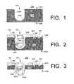
- FIG. 1shows a semiconductor wafer 104 in an integrated circuit fabrication process.
- Wafer 104includes a semiconductor substrate 110 made of monocrystalline silicon or some other semiconductor material. Transistors, capacitors, resistors, and other circuit elements (not shown), may have been formed in the wafer in, above and/or below the substrate.
- the top (or front) side 104 F of wafer 104is an “active” side which includes, or will include, the circuit elements mentioned above.
- the top portion of substrate 110will include active areas for transistors and other devices.
- the backside 104 Bis a non-active side.
- some circuit elementsmay be located at backside 104 B. Such elements may be formed after the backside etch of wafer 104 described below with reference to FIG. 3 .
- the particular location and structure, of the circuit elementsdo not limit the invention.
- Openings 124are formed in the top surface of substrate 110 . If other layers (not shown) have been formed on the top surface, these layers are removed at the location of openings 124 when the openings are formed. Sidewalls 124 S of openings 124 are vertical or have a vertical portion. In some embodiments, the entire sidewalls are vertical except at the bottom corners 124 C. The corners may be sloped and/or rounded. Openings 124 can be formed by a masked anisotropic etch using known technology. Suitable anisotropic reactive ion etching equipment is available from Surface Technology Systems plc of the United Kingdom. See also U.S. Pat. No. 6,184,060 issued Feb. 6, 2001 to O. Siniaguine, and U.S. Pat. No. 6,322,903 issued Nov. 27, 2001 to O. Siniaguine et al., both incorporated herein by reference.
- Dielectric layer 140(FIG. 2) is formed on the semiconductor surface in openings 124 .
- Dielectric 140can be BPSG or undoped silicon dioxide formed by thermal oxidation or chemical vapor deposition (CVD). See the aforementioned U.S. Pat. Nos. 6,184,060 and 6,322,903.
- An exemplary thickness of dielectric 140is 1-2 ⁇ m. Other dielectric materials, fabrication processes and dimensions can also be used.
- Dielectric 140can be patterned outside of openings 124 as needed to form circuit elements.
- Conductive layer 150is formed in openings 124 on dielectric 140 .
- Layer 150will be used to provide backside contacts on wafer 104 .
- layer 150is metal.
- layer 150is a solderable metal, or a combination of conductive layers with the bottom layer being solderable metal.
- Solderable metalsinclude copper, gold, nickel, zinc, chromium, vanadium, palladium, tin/lead, tin/indium, tin/silver, tin/bismuth, or their alloys and combinations, as known in the art.
- An exemplary thickness of layer 150is a 0.8-1.2 ⁇ m (e.g. 1 ⁇ m). Other materials and dimensions, known or to be invented, can also be used.
- Outer sidewalls 150 V of layer 150 in openings 124are vertical or include a vertical portion. In some embodiments, the entire sidewalls are vertical except at the bottom corners.
- a filler 160for example, a metal, silicon dioxide, or some other material, is formed optionally in openings 124 to increase the mechanical strength of the structure and/or improve heat dissipation. Filler 160 completely or partially fills the openings. Filler 160 can be a tungsten plug for example. In some embodiments, filler 160 and conductive layer 150 are a single layer formed from the same material in a single deposition step.
- Layers 150 , 160can be patterned as needed to form other circuit elements.
- FIG. 2shows one such element, a MOS transistor.
- the transistorhas source/drain regions 204 formed in the top surface of substrate 110 , a channel region between the source/drain regions, and a gate 208 overlying the channel region and separated therefrom by a gate dielectric.
- Layer 150 in opening 124can be connected to a source drain region 204 , a gate 208 , or other circuit elements.
- Other integrated circuit dies or waferscan be attached to the top of wafer 104 . See the aforementioned U.S. Pat. Nos. 6,184,060 and 6,322,903.
- backside processing of wafer 104exposes the conductive layer 150 on the bottom of the wafer.
- Suitable processesare described in the aforementioned U.S. Pat. Nos. 6,184,060 and 6,322,903.
- the layer 150can be exposed by an atmospheric pressure plasma etch using CF 4 .
- oxide 140becomes exposed, the oxide and the silicon 110 are etched simultaneously. Silicon 110 is etched faster than oxide 140 . Therefore, at the end of the etch, the oxide 140 protrudes down from the bottom surface of substrate 110 around the exposed contact portions 150 C of layer 150 .
- the protrusions of dielectric 140will help to insulate the silicon substrate from the solder when the contacts 150 C are soldered to another structure (see FIG. 4 ).
- dielectric 140When dielectric 140 is exposed during the backside etch, it is etched both vertically and horizontally. The horizontal etch rate may or may not be the same as the vertical etch rate. Due to the horizontal etching, dielectric 140 is thinned around the layer 150 . The exposed part of dielectric 140 is shown at 140 P. The lower portions of dielectric 140 P are exposed earlier, and therefore etched longer, than the higher portions. Consequently, at the end of the etch, dielectric 140 P is thinner at the bottom. The entire protruding portion 140 P becomes gradually thinner as it is traced down from substrate 110 . As a result, the protruding portion 140 P is more flexible at the bottom, and is less likely to be detached from contact 150 C if the contact is pulled sideways. The contact can be pulled sideways after being bonded to a substrate 410 (FIG. 4 ). The contact can be pulled sideways due to thermal expansion/contraction or during handling.
- dielectric 140protrudes down from substrate 110 by at least 1-2 ⁇ m when measured vertically.
- Contacts 150 Cprotrude down below the dielectric by about 1-100 ⁇ m or more.
- Vertical sidewall portions 150 Vprotrude down by about 1-100 ⁇ m or more below dielectric 140 .
- Substrate 410can be a wiring substrate, e.g. a printed circuit board or an intermediate packaging substrate such as used in ball grid array packaging or other packaging types.
- Substrate 410can also be an integrated circuit die or wafer, or a stack of such dies or wafers. Wafer 104 can be diced before attachment to substrate 410 , and individual dies can be attached to substrate or substrates 410 .
- Solder 420is deposited on contacts 430 formed at the top surface of substrate 410 , or the solder can be deposited on backside contacts 150 C, or both.
- the soldercan be tin or its alloys as known in the art.
- Conductive material 150is solder wettable, or includes a solder wettable layer as the bottom layer. Alternatively, before the solder is deposited, the contacts 150 C can be covered with a solder wettable material (by electroplating, for example).
- layer 150includes a solder wettable layer (e.g. copper) 150 . 1 and some other layer 150 . 2 underlying the layer 150 . 1 .
- Layer 150 . 2can be a barrier layer formed to prevent intermixing of layer 150 . 1 with dielectric 140 .
- tungsten, TiW, or tantalumcan be used to prevent intermixing of copper with silicon dioxide.
- layer 150 . 2is the bottom sub-layer of layer 150 , and layer 150 . 2 is not solder wettable.
- Layer 150 . 2is etched away to expose the solder wettable layer before the contacts 150 C are soldered to substrate 410 .
- the backside etchmay involve simultaneous etching of silicon 110 , oxide 140 , and layer 150 . 2 with a fluorine plasma (e.g. CF 4 ) as described above.
- a fluorine plasmae.g. CF 4
- the layer 150 . 2can be removed separately after the backside etch of substrate 110 and dielectric 140 .
- layer 150 . 2can be dissolved by a solder flux or the solder, or can be removed in a separate etching step before the solder flux or the solder are deposited.
- Solder 420is deposited in sufficient quantities to reach and cover a portion of the vertical surface 150 V of each contact 150 C. See FIG. 4 . Consequently, the solder bond is stronger because any mechanical forces that may pull the die or wafer 104 upward must overcome the sheer friction force at the interface between the vertical surface 150 V and the solder before the solder bond can be broken. (Such “pull-up” mechanical forces can be generated by thermal cycling or during handling.) The solder portions on the vertical surfaces 150 V also protect the solder bond if the wafer or die 104 is pulled sideways.
- Solder 420can be replaced with a conductive or anisotropic adhesive.
- the anisotropic adhesivemay fill the entire space between substrates 110 and 410 .
- a dielectric adhesivecan be introduced between the die or wafer 104 and substrate 410 .
- a dielectriccan be formed on the bottom portion of substrate 110 .
- the dielectriccan be grown selectively as described in the aforementioned U.S. Pat. No. 6,184,060.
- the dielectriccan be formed by depositing a flowable material, e.g. polyimide (not shown), over the wafer backside, curing the material, and etching the material with a blanket etch, as described in the aforementioned U.S. Pat. No. 6,322,903.
- the materialis thinner over the contacts 150 C than over the backside surface of substrate 110 , and the etch of the material exposes the contacts 150 C without exposing the substrate. In some embodiments, the etch of the material exposes some of the dielectric 140 P, and causes the dielectric 140 P to protrude from the material.
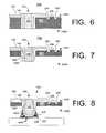
- the backside etchcan be preceded by backside grinding of substrate 110 .
- the grindingterminates before the dielectric 140 is exposed.
- the grindingmay expose dielectric 140 , and possibly even the conductive layers 150 and 160 . See FIG. 6, and see U.S. patent application Ser. No. 09/792,311 filed Feb. 22, 2001 by P. Halahan et al., entitled “Semiconductor Structures Having Multiple Conductive Layers In An Opening, And Methods For Fabricating Same”, incorporated herein by reference.
- the grindingis followed by a backside etch of substrate 110 and dielectric 140 as in FIG. 3 .
- the resulting structureis shown in FIG. 7 .
- the protruding dielectric 140 Pmay have a convex profile if before the etch the dielectric layer 140 was thicker (wider) at the bottom. See FIG. 6 . More generally, the shape of protruding dielectric 140 P may depend on the profile of dielectric 140 before the etch, on the etching process, and possibly other factors which may or may not be understood at this time. For example, the etch may include several etching steps with different ratios of the vertical etch rate to the horizontal etch rate, and the exact etch rate ratios may affect the profile of portions 140 P. The invention is not limited to any particular profile of dielectric portions 140 P or any backside processing techniques.
- the surface 150 V of conductive layer 150is not vertical but is sloped outwards with respect to through hole 124 as the surface 150 V is traced down.
- the sloped profilecan be achieved by depositing the dielectric 140 so that, at the stage of FIG. 2, the dielectric 140 gets thinner when traced in the downward direction along the sidewalls of openings 124 .
- the sloped profile of surface 150 Vis achieved by forming the openings 124 such that their sidewalls expand outwards as they go down. Techniques for forming such openings are well known.
- Solder 420reaches around the widest part of contacts 150 C and covers a portion of sloped surface 150 V. The solder bond is strengthened as a result.
- Adhesive 1010reaches around the widest part of contacts 150 C and covers a portion of sloped surface 150 V. In FIG. 10, the adhesive 1010 fills the entire space between the die or wafer 104 and substrate 410 .
- Adhesive 1010is generally dielectric but has a conductive portion 1010 . 1 between each contact 150 C and the corresponding contact 430 . Portions 1010 . 1 become conductive when contacts 150 C and 430 are pressed against each other in the process of bonding the die or wafer 104 to substrate 410 .
- the backside processing of wafer 104is performed as in the aforementioned U.S. Pat. No. 6,322,903.
- the backside etch of substrate 110exposes the dielectric 140 but not the conductive layer 150 .
- a flowable dielectric 710e.g. polyimide
- Dielectric 140protrudes from the surface of the polyimide 710 at the location of the backside contacts.
- dielectric 140is etched, possibly selectively to dielectric 710 , until the surface 150 V of layer 150 is exposed. See FIG. 12 .
- Surface 150 Vcan be vertical or sloped outwards as in FIG. 8 .
- dielectric 140does not become gradually thinner around the contacts 150 C.
- the protruding portions of dielectric 140 Pbecome gradually thinner around the contact 150 C, but the sidewalls of layer 150 and opening 124 are not vertical nor sloped outwards. The sidewalls are sloped inwards, into the opening, as the sidewalls are traced down.
- the inventionis not limited by particular materials, dimensions, fabrication techniques, or the number of openings 124 .
- the inventionis defined by the appended claims.
- the terms “top surface” and “bottom surface”are used to identify the surfaces and their position relative to each other. These terms do not mean that the structures cannot be turned upside down during or after processing, or placed at some other angle, to position the “top surface” below the “bottom surface” or in some other position relative to the “bottom surface”.
Landscapes
- Engineering & Computer Science (AREA)
- Microelectronics & Electronic Packaging (AREA)
- Power Engineering (AREA)
- Computer Hardware Design (AREA)
- Physics & Mathematics (AREA)
- Condensed Matter Physics & Semiconductors (AREA)
- General Physics & Mathematics (AREA)
- Manufacturing & Machinery (AREA)
- Internal Circuitry In Semiconductor Integrated Circuit Devices (AREA)
- Wire Bonding (AREA)
Abstract
Description
Claims (17)
Priority Applications (1)
| Application Number | Priority Date | Filing Date | Title |
|---|---|---|---|
| US10/318,833US6664129B2 (en) | 1996-10-29 | 2002-12-12 | Integrated circuits and methods for their fabrication |
Applications Claiming Priority (6)
| Application Number | Priority Date | Filing Date | Title |
|---|---|---|---|
| US3042596P | 1996-10-29 | 1996-10-29 | |
| PCT/US1997/018979WO1998019337A1 (en) | 1996-10-29 | 1997-10-27 | Integrated circuits and methods for their fabrication |
| US09/083,927US6184060B1 (en) | 1996-10-29 | 1998-05-22 | Integrated circuits and methods for their fabrication |
| US09/466,535US6639303B2 (en) | 1996-10-29 | 1999-12-17 | Integrated circuits and methods for their fabrication |
| US10/059,898US6882030B2 (en) | 1996-10-29 | 2002-01-28 | Integrated circuit structures with a conductor formed in a through hole in a semiconductor substrate and protruding from a surface of the substrate |
| US10/318,833US6664129B2 (en) | 1996-10-29 | 2002-12-12 | Integrated circuits and methods for their fabrication |
Related Parent Applications (1)
| Application Number | Title | Priority Date | Filing Date |
|---|---|---|---|
| US10/059,898DivisionUS6882030B2 (en) | 1996-10-29 | 2002-01-28 | Integrated circuit structures with a conductor formed in a through hole in a semiconductor substrate and protruding from a surface of the substrate |
Publications (2)
| Publication Number | Publication Date |
|---|---|
| US20030085460A1 US20030085460A1 (en) | 2003-05-08 |
| US6664129B2true US6664129B2 (en) | 2003-12-16 |
Family
ID=27658269
Family Applications (2)
| Application Number | Title | Priority Date | Filing Date |
|---|---|---|---|
| US10/059,898Expired - LifetimeUS6882030B2 (en) | 1996-10-29 | 2002-01-28 | Integrated circuit structures with a conductor formed in a through hole in a semiconductor substrate and protruding from a surface of the substrate |
| US10/318,833Expired - LifetimeUS6664129B2 (en) | 1996-10-29 | 2002-12-12 | Integrated circuits and methods for their fabrication |
Family Applications Before (1)
| Application Number | Title | Priority Date | Filing Date |
|---|---|---|---|
| US10/059,898Expired - LifetimeUS6882030B2 (en) | 1996-10-29 | 2002-01-28 | Integrated circuit structures with a conductor formed in a through hole in a semiconductor substrate and protruding from a surface of the substrate |
Country Status (2)
| Country | Link |
|---|---|
| US (2) | US6882030B2 (en) |
| WO (1) | WO2003065450A2 (en) |
Cited By (181)
| Publication number | Priority date | Publication date | Assignee | Title |
|---|---|---|---|---|
| US20030183920A1 (en)* | 2002-03-28 | 2003-10-02 | Goodrich Joel Lee | Hermetic electric component package |
| US20040060174A1 (en)* | 2002-09-17 | 2004-04-01 | Shinko Electric Industries Co. Ltd. | Method for producing wiring substrate |
| US20040192033A1 (en)* | 2003-01-15 | 2004-09-30 | Kazumi Hara | Semiconductor device, method of manufacturing the same, circuit board, and electronic instrument |
| US20040245623A1 (en)* | 2003-03-28 | 2004-12-09 | Kazumi Hara | Semiconductor device, circuit substrate and electronic instrument |
| US20050029630A1 (en)* | 2003-03-25 | 2005-02-10 | Yoshihide Matsuo | Manufacturing method for semiconductor device, semiconductor device, and electronic apparatus |
| US20050067685A1 (en)* | 2003-09-30 | 2005-03-31 | Chirag S. Patel | Fabrication of semiconductor dies with micro-pins and structures produced therewith |
| US20060273455A1 (en)* | 2005-06-01 | 2006-12-07 | Intel Corporation | Electronic packaging including die with through silicon via |
| US20070045837A1 (en)* | 2005-08-03 | 2007-03-01 | Seiko Epson Corporation | Semiconductor device and semiconductor chip |
| US20070049016A1 (en)* | 2005-09-01 | 2007-03-01 | Micron Technology, Inc. | Microfeature workpieces and methods for forming interconnects in microfeature workpieces |
| US20080054444A1 (en)* | 2006-08-31 | 2008-03-06 | Micron Technology, Inc. | Microfeature workpieces having interconnects and conductive backplanes, and associated systems and methods |
| US20090057912A1 (en)* | 2007-08-31 | 2009-03-05 | Micron Technology, Inc. | Partitioned through-layer via and associated systems and methods |
| US20090102021A1 (en)* | 2007-10-17 | 2009-04-23 | Chih-Hua Chen | Through-Silicon Vias and Methods for Forming the Same |
| US20090134500A1 (en)* | 2007-11-26 | 2009-05-28 | Chen-Cheng Kuo | Structures for Preventing Cross-talk Between Through-Silicon Vias and Integrated Circuits |
| US20090186430A1 (en)* | 2007-05-24 | 2009-07-23 | Chih-Hua Chen | Test Patterns for Detecting Misalignment of Through-Wafer Vias |
| US20090193584A1 (en)* | 2008-02-05 | 2009-08-06 | Standard Textile Co., Inc. | Woven contoured bed sheet with elastomeric yarns |
| US7608919B1 (en) | 2003-09-04 | 2009-10-27 | University Of Notre Dame Du Lac | Interconnect packaging systems |
| US20090283871A1 (en)* | 2008-05-14 | 2009-11-19 | Hung-Pin Chang | System, Structure, and Method of Manufacturing a Semiconductor Substrate Stack |
| US20090321888A1 (en)* | 2007-12-06 | 2009-12-31 | Taiwan Semiconductor Manufacturing Company, Ltd. | Alignment for backside illumination sensor |
| US20100032834A1 (en)* | 2008-08-08 | 2010-02-11 | Stmicroelectronics S.R.L | Method for forming bumps in substrates with through vias |
| US20100038674A1 (en)* | 2008-08-18 | 2010-02-18 | Ding-Yuan Chen | Light-Emitting Diode With Current-Spreading Region |
| US20100062693A1 (en)* | 2008-09-05 | 2010-03-11 | Taiwan Semiconductor Manufacturing Co., Ltd. | Two step method and apparatus for polishing metal and other films in semiconductor manufacturing |
| US7683458B2 (en) | 2004-09-02 | 2010-03-23 | Micron Technology, Inc. | Through-wafer interconnects for photoimager and memory wafers |
| US20100084747A1 (en)* | 2008-10-03 | 2010-04-08 | Chih-Hua Chen | Zigzag Pattern for TSV Copper Adhesion |
| US20100090304A1 (en)* | 2008-09-08 | 2010-04-15 | Taiwan Semiconductor Manufacturing Company, Ltd. | Bonding process for cmos image sensor |
| US20100117201A1 (en)* | 2008-11-13 | 2010-05-13 | Kai-Ming Ching | Cooling Channels in 3DIC Stacks |
| US20100123256A1 (en)* | 2008-11-18 | 2010-05-20 | Seiko Epson Corporation | Semiconductor device, manufacturing method thereof, and electronic apparatus |
| US20100140805A1 (en)* | 2008-12-10 | 2010-06-10 | Hung-Pin Chang | Bump Structure for Stacked Dies |
| US20100144094A1 (en)* | 2008-12-05 | 2010-06-10 | Ming-Fa Chen | Method of Forming Stacked Dies |
| US20100164109A1 (en)* | 2008-12-29 | 2010-07-01 | Wen-Chih Chiou | Backside Metal Treatment of Semiconductor Chips |
| US20100171197A1 (en)* | 2009-01-05 | 2010-07-08 | Hung-Pin Chang | Isolation Structure for Stacked Dies |
| US20100171203A1 (en)* | 2009-01-07 | 2010-07-08 | Taiwan Semiconductor Manufacturing Company | Robust TSV structure |
| US20100176494A1 (en)* | 2009-01-13 | 2010-07-15 | Ming-Fa Chen | Through-Silicon Via With Low-K Dielectric Liner |
| US20100187671A1 (en)* | 2009-01-26 | 2010-07-29 | Chuan-Yi Lin | Forming Seal Ring in an Integrated Circuit Die |
| US20100187670A1 (en)* | 2009-01-26 | 2010-07-29 | Chuan-Yi Lin | On-Chip Heat Spreader |
| US20100193954A1 (en)* | 2009-02-04 | 2010-08-05 | Max Liu | Barrier Structures and Methods for Through Substrate Vias |
| US20100194014A1 (en)* | 2009-02-02 | 2010-08-05 | Jao Sheng Huang | Semiconductor Wafer Carrier |
| US20100220226A1 (en)* | 2009-02-24 | 2010-09-02 | Taiwan Semiconductor Manufacturing Company, Ltd. | Front side implanted guard ring structure for backside illuminated image sensor |
| US20100224966A1 (en)* | 2009-03-03 | 2010-09-09 | Taiwan Semiconductor Manufacturing Company, Ltd. | Stress Barrier Structures for Semiconductor Chips |
| US20100225002A1 (en)* | 2009-03-06 | 2010-09-09 | Taiwan Semiconductor Manufacturing Company, Ltd. | Three-Dimensional System-in-Package Architecture |
| US7795134B2 (en) | 2005-06-28 | 2010-09-14 | Micron Technology, Inc. | Conductive interconnect structures and formation methods using supercritical fluids |
| US20100237502A1 (en)* | 2009-03-23 | 2010-09-23 | Taiwan Semiconductor Manufacturing Company, Ltd. | Barrier for Through-Silicon Via |
| US20100244247A1 (en)* | 2009-03-27 | 2010-09-30 | Taiwan Semiconductor Manufacturing Company, Ltd. | Via structure and via etching process of forming the same |
| US20100244284A1 (en)* | 2009-03-27 | 2010-09-30 | Taiwan Semiconductor Manufacturing Company, Ltd. | Method for ultra thin wafer handling and processing |
| US20100252934A1 (en)* | 2009-04-07 | 2010-10-07 | Taiwan Semiconductor Manufacturing Company, Ltd. | Three-Dimensional Semiconductor Architecture |
| US20100267217A1 (en)* | 2009-04-20 | 2010-10-21 | Taiwan Semiconductor Manufacturing Company, Ltd. | Backside Process for a Substrate |
| US20100276787A1 (en)* | 2009-04-30 | 2010-11-04 | Taiwan Semiconductor Manufacturing Company, Ltd. | Wafer Backside Structures Having Copper Pillars |
| US7829975B2 (en)* | 1996-12-02 | 2010-11-09 | Kabushiki Kaisha Toshiba | Multichip semiconductor device, chip therefor and method of formation thereof |
| US7829976B2 (en) | 2004-06-29 | 2010-11-09 | Micron Technology, Inc. | Microelectronic devices and methods for forming interconnects in microelectronic devices |
| US20100314758A1 (en)* | 2009-06-12 | 2010-12-16 | Taiwan Semiconductor Manufacturing Company, Ltd. | Through-silicon via structure and a process for forming the same |
| US20100330798A1 (en)* | 2009-06-26 | 2010-12-30 | Taiwan Semiconductor Manufacturing Company, Ltd. | Formation of TSV Backside Interconnects by Modifying Carrier Wafers |
| US20100330788A1 (en)* | 2009-06-30 | 2010-12-30 | Taiwan Semiconductor Manufacturing Company, Ltd. | Thin wafer handling structure and method |
| US20110006428A1 (en)* | 2009-07-08 | 2011-01-13 | Ching-Yu Lo | Liner Formation in 3DIC Structures |
| US20110027944A1 (en)* | 2009-07-30 | 2011-02-03 | Taiwan Semiconductor Maufacturing Company, Ltd. | Method of forming electrical connections |
| US7884015B2 (en) | 2007-12-06 | 2011-02-08 | Micron Technology, Inc. | Methods for forming interconnects in microelectronic workpieces and microelectronic workpieces formed using such methods |
| US20110035937A1 (en)* | 2009-08-14 | 2011-02-17 | Taiwan Semiconductor Manufacturing Company, Ltd. | Semiconductor Wafer Carrier and Method of Manufacturing |
| US20110065238A1 (en)* | 2009-09-14 | 2011-03-17 | Taiwan Semiconductor Manufacturing Company, Ltd. | Protection layer for adhesive material at wafer edge |
| US20110062564A1 (en)* | 2009-09-17 | 2011-03-17 | Gruenhagen Michael D | Semiconductor die containing lateral edge shapes and textures |
| US7915736B2 (en) | 2005-09-01 | 2011-03-29 | Micron Technology, Inc. | Microfeature workpieces and methods for forming interconnects in microfeature workpieces |
| US20110078127A1 (en)* | 2009-09-27 | 2011-03-31 | Alibaba Group Holding Limited | Searching for information based on generic attributes of the query |
| US20110081749A1 (en)* | 2009-10-01 | 2011-04-07 | Taiwan Semiconductor Manufacturing Company, Ltd. | Surface modification for handling wafer thinning process |
| US20110084365A1 (en)* | 2009-10-09 | 2011-04-14 | Taiwan Semiconductor Manufacturing Company, Ltd. | Through Silicon Via (TSV) Wire Bond Architecture |
| US20110101527A1 (en)* | 2009-11-05 | 2011-05-05 | Taiwan Semiconductor Manufacturing Company, Ltd. | Mechanisms for forming copper pillar bumps |
| US20110108940A1 (en)* | 2009-11-06 | 2011-05-12 | Taiwan Semiconductor Manufacturing Company, Ltd. | Method of fabricating backside-illuminated image sensor |
| US20110108986A1 (en)* | 2009-11-09 | 2011-05-12 | Taiwan Semiconductor Manufacturing Company, Ltd. | Through-silicon via structure and a process for forming the same |
| US20110133335A1 (en)* | 2008-12-31 | 2011-06-09 | Taiwan Semiconductor Manufacturing Company, Ltd. | Through-Silicon Via With Air Gap |
| US7973411B2 (en) | 2006-08-28 | 2011-07-05 | Micron Technology, Inc. | Microfeature workpieces having conductive interconnect structures formed by chemically reactive processes, and associated systems and methods |
| US20110169168A1 (en)* | 2009-02-24 | 2011-07-14 | Taiwan Semiconductor Manufacturing Company, Ltd. | Through-silicon via formed with a post passivation interconnect structure |
| US20110177655A1 (en)* | 2007-06-27 | 2011-07-21 | Taiwan Semiconductor Manufacturing Company, Ltd. | Formation of Through Via before Contact Processing |
| US20110193221A1 (en)* | 2010-02-05 | 2011-08-11 | Taiwan Semiconductor Manufacturing Company, Ltd. | 3DIC Architecture with Interposer for Bonding Dies |
| US20110193219A1 (en)* | 2010-02-09 | 2011-08-11 | Taiwan Seimconductor Manufacturing Company, Ltd. | Semiconductor device and semiconductor assembly with lead-free solder |
| US20110198721A1 (en)* | 2010-02-12 | 2011-08-18 | Taiwan Semiconductor Manufacturing Company, Ltd. | Method for thinning a wafer |
| US20110198747A1 (en)* | 2010-02-16 | 2011-08-18 | Taiwan Semicondcutor Manufactoring Company, Ltd. | Conductive pillar structure for semiconductor substrate and method of manufacture |
| US20110198638A1 (en)* | 2010-02-16 | 2011-08-18 | Taiwan Semiconductor Manufacturing Company, Ltd. | Light-emitting diode (led) package systems |
| US20110217841A1 (en)* | 2009-10-22 | 2011-09-08 | Taiwan Semiconductor Manufacturing Company, Ltd. | Method of forming through silicon via with dummy structure |
| US8084866B2 (en) | 2003-12-10 | 2011-12-27 | Micron Technology, Inc. | Microelectronic devices and methods for filling vias in microelectronic devices |
| US8102039B2 (en) | 2006-08-11 | 2012-01-24 | Sanyo Semiconductor Co., Ltd. | Semiconductor device and manufacturing method thereof |
| US8174124B2 (en) | 2010-04-08 | 2012-05-08 | Taiwan Semiconductor Manufacturing Co., Ltd. | Dummy pattern in wafer backside routing |
| US20120175784A1 (en)* | 2008-12-08 | 2012-07-12 | Stats Chippac, Ltd. | Semiconductor Device and Method of Forming Vertical Interconnect Structure in Substrate for IPD and Baseband Circuit Separated by High-Resistivity Molding Compound |
| US8222139B2 (en) | 2010-03-30 | 2012-07-17 | Taiwan Semiconductor Manufacturing Company, Ltd. | Chemical mechanical polishing (CMP) processing of through-silicon via (TSV) and contact plug simultaneously |
| US8236584B1 (en) | 2011-02-11 | 2012-08-07 | Tsmc Solid State Lighting Ltd. | Method of forming a light emitting diode emitter substrate with highly reflective metal bonding |
| US8247906B2 (en) | 2009-07-06 | 2012-08-21 | Taiwan Semiconductor Manufacturing Company, Ltd. | Supplying power to integrated circuits using a grid matrix formed of through-silicon vias |
| US8319336B2 (en) | 2010-07-08 | 2012-11-27 | Taiwan Semiconductor Manufacturing Company, Ltd. | Reduction of etch microloading for through silicon vias |
| US8322031B2 (en) | 2004-08-27 | 2012-12-04 | Micron Technology, Inc. | Method of manufacturing an interposer |
| US8324738B2 (en) | 2009-09-01 | 2012-12-04 | Taiwan Semiconductor Manufacturing Company, Ltd. | Self-aligned protection layer for copper post structure |
| US8338939B2 (en) | 2010-07-12 | 2012-12-25 | Taiwan Semiconductor Manufacturing Company, Ltd. | TSV formation processes using TSV-last approach |
| US8362591B2 (en) | 2010-06-08 | 2013-01-29 | Taiwan Semiconductor Manufacturing Co., Ltd. | Integrated circuits and methods of forming the same |
| US8411459B2 (en) | 2010-06-10 | 2013-04-02 | Taiwan Semiconductor Manufacturing Company, Ltd | Interposer-on-glass package structures |
| US8441124B2 (en) | 2010-04-29 | 2013-05-14 | Taiwan Semiconductor Manufacturing Company, Ltd. | Cu pillar bump with non-metal sidewall protection structure |
| US8445296B2 (en) | 2011-07-22 | 2013-05-21 | Taiwan Semiconductor Manufacturing Company, Ltd. | Apparatus and methods for end point determination in reactive ion etching |
| US8456008B2 (en) | 2007-12-21 | 2013-06-04 | Taiwan Semiconductor Manufacturing Company, Ltd. | Structure and process for the formation of TSVs |
| US8455995B2 (en) | 2010-04-16 | 2013-06-04 | Taiwan Semiconductor Manufacturing Company, Ltd. | TSVs with different sizes in interposers for bonding dies |
| US8461045B2 (en) | 2008-10-09 | 2013-06-11 | Taiwan Semiconductor Manufacturing Company, Ltd. | Bond pad connection to redistribution lines having tapered profiles |
| US8466059B2 (en) | 2010-03-30 | 2013-06-18 | Taiwan Semiconductor Manufacturing Company, Ltd. | Multi-layer interconnect structure for stacked dies |
| US20130157456A1 (en)* | 2011-01-12 | 2013-06-20 | Darrell G. Hill | Methods relating to the fabrication of devices having conductive substrate vias with catch-pad etch-stops |
| US8471358B2 (en) | 2010-06-01 | 2013-06-25 | Taiwan Semiconductor Manufacturing Company, Ltd. | 3D inductor and transformer |
| US8476735B2 (en) | 2007-05-29 | 2013-07-02 | Taiwan Semiconductor Manufacturing Company, Ltd. | Programmable semiconductor interposer for electronic package and method of forming |
| US8487410B2 (en) | 2011-04-13 | 2013-07-16 | Taiwan Semiconductor Manufacturing Company, Ltd. | Through-silicon vias for semicondcutor substrate and method of manufacture |
| US8500182B2 (en) | 2010-06-17 | 2013-08-06 | Taiwan Semiconductor Manufacturing Company, Ltd. | Vacuum wafer carriers for strengthening thin wafers |
| US8502338B2 (en) | 2010-09-09 | 2013-08-06 | Taiwan Semiconductor Manufacturing Company, Ltd. | Through-substrate via waveguides |
| US8501587B2 (en) | 2009-01-13 | 2013-08-06 | Taiwan Semiconductor Manufacturing Company, Ltd. | Stacked integrated chips and methods of fabrication thereof |
| US8507358B2 (en) | 2010-08-27 | 2013-08-13 | Taiwan Semiconductor Manufacturing Company, Ltd. | Composite wafer semiconductor |
| US8507940B2 (en) | 2010-04-05 | 2013-08-13 | Taiwan Semiconductor Manufacturing Company, Ltd. | Heat dissipation by through silicon plugs |
| US8519409B2 (en) | 2010-11-15 | 2013-08-27 | Taiwan Semiconductor Manufacturing Company, Ltd. | Light emitting diode components integrated with thermoelectric devices |
| US8519538B2 (en) | 2010-04-28 | 2013-08-27 | Taiwan Semiconductor Manufacturing Company, Ltd. | Laser etch via formation |
| US8525278B2 (en) | 2011-08-19 | 2013-09-03 | Taiwan Semiconductor Manufacturing Company, Ltd. | MEMS device having chip scale packaging |
| US8525343B2 (en) | 2010-09-28 | 2013-09-03 | Taiwan Semiconductor Manufacturing Company, Ltd. | Device with through-silicon via (TSV) and method of forming the same |
| US8531035B2 (en) | 2011-07-01 | 2013-09-10 | Taiwan Semiconductor Manufacturing Company, Ltd. | Interconnect barrier structure and method |
| US8546235B2 (en) | 2011-05-05 | 2013-10-01 | Taiwan Semiconductor Manufacturing Company, Ltd. | Integrated circuits including metal-insulator-metal capacitors and methods of forming the same |
| US8546254B2 (en) | 2010-08-19 | 2013-10-01 | Taiwan Semiconductor Manufacturing Company, Ltd. | Mechanisms for forming copper pillar bumps using patterned anodes |
| US8546886B2 (en) | 2011-08-24 | 2013-10-01 | Taiwan Semiconductor Manufacturing Company, Ltd. | Controlling the device performance by forming a stressed backside dielectric layer |
| US8546953B2 (en) | 2011-12-13 | 2013-10-01 | Taiwan Semiconductor Manufacturing Co., Ltd. | Through silicon via (TSV) isolation structures for noise reduction in 3D integrated circuit |
| US8552485B2 (en) | 2011-06-15 | 2013-10-08 | Taiwan Semiconductor Manufacturing Company, Ltd. | Semiconductor structure having metal-insulator-metal capacitor structure |
| US8567837B2 (en) | 2010-11-24 | 2013-10-29 | Taiwan Semiconductor Manufacturing Company, Ltd. | Reconfigurable guide pin design for centering wafers having different sizes |
| US8580647B2 (en) | 2011-12-19 | 2013-11-12 | Taiwan Semiconductor Manufacturing Company, Ltd. | Inductors with through VIAS |
| US8580682B2 (en) | 2010-09-30 | 2013-11-12 | Taiwan Semiconductor Manufacturing Company, Ltd. | Cost-effective TSV formation |
| US8587127B2 (en) | 2011-06-15 | 2013-11-19 | Taiwan Semiconductor Manufacturing Company, Ltd. | Semiconductor structures and methods of forming the same |
| US8604491B2 (en) | 2011-07-21 | 2013-12-10 | Tsmc Solid State Lighting Ltd. | Wafer level photonic device die structure and method of making the same |
| US8604619B2 (en) | 2011-08-31 | 2013-12-10 | Taiwan Semiconductor Manufacturing Company, Ltd. | Through silicon via keep out zone formation along different crystal orientations |
| US8610247B2 (en) | 2011-12-30 | 2013-12-17 | Taiwan Semiconductor Manufacturing Company, Ltd. | Structure and method for a transformer with magnetic features |
| US8618631B2 (en) | 2012-02-14 | 2013-12-31 | Taiwan Semiconductor Manufacturing Co., Ltd. | On-chip ferrite bead inductor |
| US8629042B2 (en) | 2008-12-08 | 2014-01-14 | Taiwan Semiconductor Manufacturing Company, Ltd. | Method for stacking semiconductor dies |
| US8629563B2 (en) | 2007-07-16 | 2014-01-14 | Taiwan Semiconductor Manufacturing Company, Ltd. | Method for packaging semiconductor dies having through-silicon vias |
| US8659126B2 (en) | 2011-12-07 | 2014-02-25 | Taiwan Semiconductor Manufacturing Company, Ltd. | Integrated circuit ground shielding structure |
| US8664562B2 (en) | 2004-05-05 | 2014-03-04 | Micron Technology, Inc. | Systems and methods for forming apertures in microfeature workpieces |
| US8674510B2 (en) | 2010-07-29 | 2014-03-18 | Taiwan Semiconductor Manufacturing Company, Ltd. | Three-dimensional integrated circuit structure having improved power and thermal management |
| US8674883B2 (en) | 2011-05-24 | 2014-03-18 | Taiwan Semiconductor Manufacturing Company, Ltd. | Antenna using through-silicon via |
| US8686526B2 (en) | 2006-11-20 | 2014-04-01 | Semiconductor Components Industries, Llc | Semiconductor device and method of manufacturing the same |
| US8693163B2 (en) | 2010-09-01 | 2014-04-08 | Taiwan Semiconductor Manufacturing Company, Ltd. | Cylindrical embedded capacitors |
| US8703609B2 (en) | 2007-08-24 | 2014-04-22 | Taiwan Semiconductor Manufacturing Company, Ltd. | Through-substrate via for semiconductor device |
| US8716131B2 (en) | 2008-08-05 | 2014-05-06 | Taiwan Semiconductor Manufacturing Company, Ltd. | Through silicon via layout |
| US8716128B2 (en) | 2011-04-14 | 2014-05-06 | Tsmc Solid State Lighting Ltd. | Methods of forming through silicon via openings |
| US8722540B2 (en) | 2010-07-22 | 2014-05-13 | Taiwan Semiconductor Manufacturing Company, Ltd. | Controlling defects in thin wafer handling |
| US8736050B2 (en) | 2009-09-03 | 2014-05-27 | Taiwan Semiconductor Manufacturing Company, Ltd. | Front side copper post joint structure for temporary bond in TSV application |
| US8748284B2 (en) | 2011-08-12 | 2014-06-10 | Taiwan Semiconductor Manufacturing Company, Ltd. | Method of manufacturing decoupling MIM capacitor designs for interposers |
| US8766409B2 (en) | 2011-06-24 | 2014-07-01 | Taiwan Semiconductor Manufacturing Co., Ltd. | Method and structure for through-silicon via (TSV) with diffused isolation well |
| US8766408B2 (en)* | 2006-03-07 | 2014-07-01 | Semiconductor Components Industries, Llc | Semiconductor device and manufacturing method thereof |
| US8773866B2 (en) | 2010-12-10 | 2014-07-08 | Taiwan Semiconductor Manufacturing Company, Ltd. | Radio-frequency packaging with reduced RF loss |
| US8791549B2 (en) | 2009-09-22 | 2014-07-29 | Taiwan Semiconductor Manufacturing Company, Ltd. | Wafer backside interconnect structure connected to TSVs |
| US8803322B2 (en) | 2011-10-13 | 2014-08-12 | Taiwan Semiconductor Manufacturing Company, Ltd. | Through substrate via structures and methods of forming the same |
| US8803316B2 (en) | 2011-12-06 | 2014-08-12 | Taiwan Semiconductor Manufacturing Company, Ltd. | TSV structures and methods for forming the same |
| US8809073B2 (en) | 2011-08-03 | 2014-08-19 | Taiwan Semiconductor Manufacturing Company, Ltd. | Apparatus and methods for de-embedding through substrate vias |
| US8836116B2 (en) | 2010-10-21 | 2014-09-16 | Taiwan Semiconductor Manufacturing Company, Ltd. | Wafer level packaging of micro-electro-mechanical systems (MEMS) and complementary metal-oxide-semiconductor (CMOS) substrates |
| US8841766B2 (en) | 2009-07-30 | 2014-09-23 | Taiwan Semiconductor Manufacturing Company, Ltd. | Cu pillar bump with non-metal sidewall protection structure |
| US8846499B2 (en) | 2010-08-17 | 2014-09-30 | Taiwan Semiconductor Manufacturing Company, Ltd. | Composite carrier structure |
| US8860114B2 (en) | 2012-03-02 | 2014-10-14 | Taiwan Semiconductor Manufacturing Company, Ltd. | Structure and method for a fishbone differential capacitor |
| US8866301B2 (en) | 2010-05-18 | 2014-10-21 | Taiwan Semiconductor Manufacturing Company, Ltd. | Package systems having interposers with interconnection structures |
| US8872345B2 (en) | 2011-07-07 | 2014-10-28 | Taiwan Semiconductor Manufacturing Company, Ltd. | Forming grounded through-silicon vias in a semiconductor substrate |
| US8890293B2 (en) | 2011-12-16 | 2014-11-18 | Taiwan Semiconductor Manufacturing Company, Ltd. | Guard ring for through vias |
| US8896136B2 (en) | 2010-06-30 | 2014-11-25 | Taiwan Semiconductor Manufacturing Company, Ltd. | Alignment mark and method of formation |
| US8896089B2 (en) | 2011-11-09 | 2014-11-25 | Taiwan Semiconductor Manufacturing Company, Ltd. | Interposers for semiconductor devices and methods of manufacture thereof |
| US8900994B2 (en) | 2011-06-09 | 2014-12-02 | Taiwan Semiconductor Manufacturing Company, Ltd. | Method for producing a protective structure |
| US8928159B2 (en) | 2010-09-02 | 2015-01-06 | Taiwan Semiconductor Manufacturing & Company, Ltd. | Alignment marks in substrate having through-substrate via (TSV) |
| US8928127B2 (en) | 2010-09-24 | 2015-01-06 | Taiwan Semiconductor Manufacturing Company, Ltd. | Noise decoupling structure with through-substrate vias |
| US8999179B2 (en) | 2010-07-13 | 2015-04-07 | Taiwan Semiconductor Manufacturing Company, Ltd. | Conductive vias in a substrate |
| US9018758B2 (en) | 2010-06-02 | 2015-04-28 | Taiwan Semiconductor Manufacturing Company, Ltd. | Cu pillar bump with non-metal sidewall spacer and metal top cap |
| US9041152B2 (en) | 2013-03-14 | 2015-05-26 | Taiwan Semiconductor Manufacturing Company, Ltd. | Inductor with magnetic material |
| US9048233B2 (en) | 2010-05-26 | 2015-06-02 | Taiwan Semiconductor Manufacturing Company, Ltd. | Package systems having interposers |
| US9059262B2 (en) | 2011-02-24 | 2015-06-16 | Taiwan Semiconductor Manufacturing Company, Ltd. | Integrated circuits including conductive structures through a substrate and methods of making the same |
| US9059026B2 (en) | 2010-06-01 | 2015-06-16 | Taiwan Semiconductor Manufacturing Company, Ltd. | 3-D inductor and transformer |
| US9087838B2 (en) | 2011-10-25 | 2015-07-21 | Taiwan Semiconductor Manufacturing Company, Ltd. | Structure and method for a high-K transformer with capacitive coupling |
| US9139420B2 (en) | 2012-04-18 | 2015-09-22 | Taiwan Semiconductor Manufacturing Company, Ltd. | MEMS device structure and methods of forming same |
| US9142586B2 (en) | 2009-02-24 | 2015-09-22 | Taiwan Semiconductor Manufacturing Company, Ltd. | Pad design for backside illuminated image sensor |
| US9153462B2 (en) | 2010-12-09 | 2015-10-06 | Taiwan Semiconductor Manufacturing Company, Ltd. | Spin chuck for thin wafer cleaning |
| US9159907B2 (en) | 2011-08-04 | 2015-10-13 | Taiwan Semiconductor Manufacturing Company, Ltd. | Hybrid film for protecting MTJ stacks of MRAM |
| US9190325B2 (en) | 2010-09-30 | 2015-11-17 | Taiwan Semiconductor Manufacturing Company, Ltd. | TSV formation |
| US9293521B2 (en) | 2012-03-02 | 2016-03-22 | Taiwan Semiconductor Manufacturing Co., Ltd. | Concentric capacitor structure |
| US9293366B2 (en) | 2010-04-28 | 2016-03-22 | Taiwan Semiconductor Manufacturing Company, Ltd. | Through-substrate vias with improved connections |
| US9299594B2 (en) | 2010-07-27 | 2016-03-29 | Taiwan Semiconductor Manufacturing Company, Ltd. | Substrate bonding system and method of modifying the same |
| US9305769B2 (en) | 2009-06-30 | 2016-04-05 | Taiwan Semiconductor Manufacturing Company, Ltd. | Thin wafer handling method |
| US9312432B2 (en) | 2012-03-13 | 2016-04-12 | Tsmc Solid State Lighting Ltd. | Growing an improved P-GaN layer of an LED through pressure ramping |
| US9390949B2 (en) | 2011-11-29 | 2016-07-12 | Taiwan Semiconductor Manufacturing Company, Ltd. | Wafer debonding and cleaning apparatus and method of use |
| US9484211B2 (en) | 2013-01-24 | 2016-11-01 | Taiwan Semiconductor Manufacturing Company, Ltd. | Etchant and etching process |
| US9490133B2 (en) | 2013-01-24 | 2016-11-08 | Taiwan Semiconductor Manufacturing Company, Ltd. | Etching apparatus |
| US9524945B2 (en) | 2010-05-18 | 2016-12-20 | Taiwan Semiconductor Manufacturing Company, Ltd. | Cu pillar bump with L-shaped non-metal sidewall protection structure |
| US9583365B2 (en) | 2012-05-25 | 2017-02-28 | Taiwan Semiconductor Manufacturing Company, Ltd. | Method of forming interconnects for three dimensional integrated circuit |
| US9620473B1 (en) | 2013-01-18 | 2017-04-11 | University Of Notre Dame Du Lac | Quilt packaging system with interdigitated interconnecting nodules for inter-chip alignment |
| US9618712B2 (en) | 2012-02-23 | 2017-04-11 | Taiwan Semiconductor Manufacturing Company, Ltd. | Optical bench on substrate and method of making the same |
| US9748106B2 (en)* | 2016-01-21 | 2017-08-29 | Micron Technology, Inc. | Method for fabricating semiconductor package |
| US10180547B2 (en) | 2012-02-23 | 2019-01-15 | Taiwan Semiconductor Manufacturing Company, Ltd. | Optical bench on substrate |
| US10381254B2 (en) | 2011-11-29 | 2019-08-13 | Taiwan Semiconductor Manufacturing Co., Ltd. | Wafer debonding and cleaning apparatus and method |
| US11264262B2 (en) | 2011-11-29 | 2022-03-01 | Taiwan Semiconductor Manufacturing Company, Ltd. | Wafer debonding and cleaning apparatus |
Families Citing this family (50)
| Publication number | Priority date | Publication date | Assignee | Title |
|---|---|---|---|---|
| US20060246621A1 (en)* | 2002-02-14 | 2006-11-02 | Intel Corporation | Microelectronic die including thermally conductive structure in a substrate thereof and method of forming same |
| US20030151132A1 (en)* | 2002-02-14 | 2003-08-14 | Crippen Warren Stuart | Microelectronic die providing improved heat dissipation, and method of packaging same |
| US6762076B2 (en)* | 2002-02-20 | 2004-07-13 | Intel Corporation | Process of vertically stacking multiple wafers supporting different active integrated circuit (IC) devices |
| JP2003273155A (en)* | 2002-03-18 | 2003-09-26 | Fujitsu Ltd | Semiconductor device and manufacturing method thereof |
| JP4110390B2 (en)* | 2002-03-19 | 2008-07-02 | セイコーエプソン株式会社 | Manufacturing method of semiconductor device |
| JP2003318178A (en)* | 2002-04-24 | 2003-11-07 | Seiko Epson Corp | Semiconductor device and its manufacturing method, circuit board, and electronic equipment |
| US6903442B2 (en)* | 2002-08-29 | 2005-06-07 | Micron Technology, Inc. | Semiconductor component having backside pin contacts |
| TW569416B (en)* | 2002-12-19 | 2004-01-01 | Via Tech Inc | High density multi-chip module structure and manufacturing method thereof |
| JP4072677B2 (en)* | 2003-01-15 | 2008-04-09 | セイコーエプソン株式会社 | Semiconductor chip, semiconductor wafer, semiconductor device and manufacturing method thereof, circuit board, and electronic equipment |
| JP3696208B2 (en)* | 2003-01-22 | 2005-09-14 | 株式会社東芝 | Semiconductor device |
| US6897148B2 (en) | 2003-04-09 | 2005-05-24 | Tru-Si Technologies, Inc. | Electroplating and electroless plating of conductive materials into openings, and structures obtained thereby |
| DE10326507A1 (en)* | 2003-06-12 | 2005-01-13 | Infineon Technologies Ag | A method of making a fracture resistant disc shaped article and associated semiconductor circuit assembly |
| DE10326508A1 (en)* | 2003-06-12 | 2005-01-13 | Infineon Technologies Ag | Semiconductor circuit arrangement comprises a thin carrier substrate containing semiconductor components, a galvanic seed layer, a galvanic filler material galvanically formed on the seed layer and a material resistant to shearing stress |
| JP3646720B2 (en)* | 2003-06-19 | 2005-05-11 | セイコーエプソン株式会社 | Semiconductor device and manufacturing method thereof, circuit board, and electronic apparatus |
| DE10342559B3 (en)* | 2003-09-15 | 2005-04-14 | Infineon Technologies Ag | Edge structure of power semiconductor component includes electrically- conducting layer deposited on parts of insulating layer in contact with region between conductivity types. |
| JP2005129904A (en)* | 2003-09-29 | 2005-05-19 | Sanyo Electric Co Ltd | Semiconductor device and method of manufacturing the same |
| US7176128B2 (en)* | 2004-01-12 | 2007-02-13 | Infineon Technologies Ag | Method for fabrication of a contact structure |
| US7012017B2 (en)* | 2004-01-29 | 2006-03-14 | 3M Innovative Properties Company | Partially etched dielectric film with conductive features |
| EP1577948A1 (en)* | 2004-03-16 | 2005-09-21 | Irvine Sensors Corp. | Stacked microelectric module with vertical interconnect vias |
| US7654956B2 (en)* | 2004-07-13 | 2010-02-02 | Dexcom, Inc. | Transcutaneous analyte sensor |
| US7491582B2 (en)* | 2004-08-31 | 2009-02-17 | Seiko Epson Corporation | Method for manufacturing semiconductor device and semiconductor device |
| US7271482B2 (en)* | 2004-12-30 | 2007-09-18 | Micron Technology, Inc. | Methods for forming interconnects in microelectronic workpieces and microelectronic workpieces formed using such methods |
| US7772115B2 (en)* | 2005-09-01 | 2010-08-10 | Micron Technology, Inc. | Methods for forming through-wafer interconnects, intermediate structures so formed, and devices and systems having at least one solder dam structure |
| US8154105B2 (en)* | 2005-09-22 | 2012-04-10 | International Rectifier Corporation | Flip chip semiconductor device and process of its manufacture |
| US7633167B2 (en) | 2005-09-29 | 2009-12-15 | Nec Electronics Corporation | Semiconductor device and method for manufacturing same |
| JP4404139B2 (en)* | 2005-10-26 | 2010-01-27 | 株式会社村田製作所 | Multilayer substrate, electronic device, and method of manufacturing multilayer substrate |
| TWI293499B (en)* | 2006-01-25 | 2008-02-11 | Advanced Semiconductor Eng | Three dimensional package and method of making the same |
| WO2008087578A2 (en)* | 2007-01-17 | 2008-07-24 | Nxp B.V. | A system-in-package with through substrate via holes |
| US7977798B2 (en)* | 2007-07-26 | 2011-07-12 | Infineon Technologies Ag | Integrated circuit having a semiconductor substrate with a barrier layer |
| KR100905784B1 (en)* | 2007-08-16 | 2009-07-02 | 주식회사 하이닉스반도체 | Through-electrode for semiconductor package and semiconductor package having same |
| KR100886720B1 (en)* | 2007-10-30 | 2009-03-04 | 주식회사 하이닉스반도체 | Laminated semiconductor package and method for manufacturing same |
| KR20090047776A (en)* | 2007-11-08 | 2009-05-13 | 삼성전자주식회사 | Semiconductor element and method of forming the same |
| SG156550A1 (en)* | 2008-05-06 | 2009-11-26 | Gautham Viswanadam | Wafer level integration module with interconnects |
| US8329573B2 (en) | 2008-05-06 | 2012-12-11 | Gautham Viswanadam | Wafer level integration module having controlled resistivity interconnects |
| US7833895B2 (en)* | 2008-05-12 | 2010-11-16 | Texas Instruments Incorporated | TSVS having chemically exposed TSV tips for integrated circuit devices |
| US7872332B2 (en) | 2008-09-11 | 2011-01-18 | Micron Technology, Inc. | Interconnect structures for stacked dies, including penetrating structures for through-silicon vias, and associated systems and methods |
| US8030780B2 (en) | 2008-10-16 | 2011-10-04 | Micron Technology, Inc. | Semiconductor substrates with unitary vias and via terminals, and associated systems and methods |
| US8102029B2 (en)* | 2008-10-31 | 2012-01-24 | Fairchild Semiconductor Corporation | Wafer level buck converter |
| JP5985136B2 (en)* | 2009-03-19 | 2016-09-06 | ソニー株式会社 | SEMICONDUCTOR DEVICE, ITS MANUFACTURING METHOD, AND ELECTRONIC DEVICE |
| US9299664B2 (en)* | 2010-01-18 | 2016-03-29 | Semiconductor Components Industries, Llc | Method of forming an EM protected semiconductor die |
| US8324511B1 (en) | 2010-04-06 | 2012-12-04 | Amkor Technology, Inc. | Through via nub reveal method and structure |
| US8440554B1 (en)* | 2010-08-02 | 2013-05-14 | Amkor Technology, Inc. | Through via connected backside embedded circuit features structure and method |
| US8487445B1 (en) | 2010-10-05 | 2013-07-16 | Amkor Technology, Inc. | Semiconductor device having through electrodes protruding from dielectric layer |
| US8216936B1 (en)* | 2010-10-21 | 2012-07-10 | Xilinx, Inc. | Low capacitance electrical connection via |
| US8390130B1 (en) | 2011-01-06 | 2013-03-05 | Amkor Technology, Inc. | Through via recessed reveal structure and method |
| US20120193788A1 (en)* | 2011-01-31 | 2012-08-02 | Advanced Micro Devices, Inc. | Stacked semiconductor chips packaging |
| KR101620767B1 (en)* | 2011-10-28 | 2016-05-12 | 인텔 코포레이션 | 3d interconnect structure comprising fine pitch single damascene backside metal redistribution lines combined with through-silicon vias |
| US8952542B2 (en)* | 2012-11-14 | 2015-02-10 | Advanced Semiconductor Engineering, Inc. | Method for dicing a semiconductor wafer having through silicon vias and resultant structures |
| US10418311B2 (en) | 2017-03-28 | 2019-09-17 | Micron Technology, Inc. | Method of forming vias using silicon on insulator substrate |
| US11521923B2 (en)* | 2018-05-24 | 2022-12-06 | Intel Corporation | Integrated circuit package supports |
Citations (94)
| Publication number | Priority date | Publication date | Assignee | Title |
|---|---|---|---|---|
| US3739463A (en) | 1971-10-18 | 1973-06-19 | Gen Electric | Method for lead attachment to pellets mounted in wafer alignment |
| US3761782A (en) | 1971-05-19 | 1973-09-25 | Signetics Corp | Semiconductor structure, assembly and method |
| US3810129A (en) | 1972-10-19 | 1974-05-07 | Ibm | Memory system restoration |
| US3838501A (en) | 1973-02-09 | 1974-10-01 | Honeywell Inf Systems | Method in microcircuit package assembly providing nonabrasive, electrically passive edges on integrated circuit chips |
| US3881884A (en) | 1973-10-12 | 1975-05-06 | Ibm | Method for the formation of corrosion resistant electronic interconnections |
| US3991296A (en) | 1974-11-15 | 1976-11-09 | Nippon Electric Company, Ltd. | Apparatus for forming grooves on a wafer by use of a laser |
| US3993917A (en) | 1975-05-29 | 1976-11-23 | International Business Machines Corporation | Parameter independent FET sense amplifier |
| US4139401A (en) | 1963-12-04 | 1979-02-13 | Rockwell International Corporation | Method of producing electrically isolated semiconductor devices on common crystalline substrate |
| US4141135A (en) | 1975-10-14 | 1979-02-27 | Thomson-Csf | Semiconductor process using lapped substrate and lapped low resistivity semiconductor carrier |
| US4368106A (en) | 1980-10-27 | 1983-01-11 | General Electric Company | Implantation of electrical feed-through conductors |
| US4394712A (en) | 1981-03-18 | 1983-07-19 | General Electric Company | Alignment-enhancing feed-through conductors for stackable silicon-on-sapphire wafers |
| US4463336A (en) | 1981-12-28 | 1984-07-31 | United Technologies Corporation | Ultra-thin microelectronic pressure sensors |
| US4467518A (en) | 1981-05-19 | 1984-08-28 | Ibm Corporation | Process for fabrication of stacked, complementary MOS field effect transistor circuits |
| US4603341A (en) | 1983-09-08 | 1986-07-29 | International Business Machines Corporation | Stacked double dense read only memory |
| US4612083A (en) | 1984-07-20 | 1986-09-16 | Nec Corporation | Process of fabricating three-dimensional semiconductor device |
| US4628174A (en) | 1984-09-17 | 1986-12-09 | General Electric Company | Forming electrical conductors in long microdiameter holes |
| US4722130A (en) | 1984-11-07 | 1988-02-02 | Kabushiki Kaisha Toshiba | Method of manufacturing a semiconductor device |
| US4729971A (en) | 1987-03-31 | 1988-03-08 | Microwave Semiconductor Corporation | Semiconductor wafer dicing techniques |
| US4769738A (en) | 1986-12-12 | 1988-09-06 | Fuji Electric Co., Ltd. | Electrostatic capacitive pressure sensor |
| US4807021A (en) | 1986-03-10 | 1989-02-21 | Kabushiki Kaisha Toshiba | Semiconductor device having stacking structure |
| US4822755A (en) | 1988-04-25 | 1989-04-18 | Xerox Corporation | Method of fabricating large area semiconductor arrays |
| US4842699A (en) | 1988-05-10 | 1989-06-27 | Avantek, Inc. | Method of selective via-hole and heat sink plating using a metal mask |
| US4897708A (en) | 1986-07-17 | 1990-01-30 | Laser Dynamics, Inc. | Semiconductor wafer array |
| US4939568A (en) | 1986-03-20 | 1990-07-03 | Fujitsu Limited | Three-dimensional integrated circuit and manufacturing method thereof |
| US4954458A (en) | 1982-06-03 | 1990-09-04 | Texas Instruments Incorporated | Method of forming a three dimensional integrated circuit structure |
| US4978639A (en) | 1989-01-10 | 1990-12-18 | Avantek, Inc. | Method for the simultaneous formation of via-holes and wraparound plating on semiconductor chips |
| US4996587A (en) | 1989-04-10 | 1991-02-26 | International Business Machines Corporation | Integrated semiconductor chip package |
| US5024970A (en) | 1989-06-27 | 1991-06-18 | Mitsubishi Denki Kabushiki Kaisha | Method of obtaining semiconductor chips |
| US5064771A (en) | 1990-04-13 | 1991-11-12 | Grumman Aerospace Corporation | Method of forming crystal array |
| US5071792A (en) | 1990-11-05 | 1991-12-10 | Harris Corporation | Process for forming extremely thin integrated circuit dice |
| US5135878A (en) | 1990-08-28 | 1992-08-04 | Solid State Devices, Inc. | Schottky diode |
| US5160987A (en) | 1989-10-26 | 1992-11-03 | International Business Machines Corporation | Three-dimensional semiconductor structures formed from planar layers |
| US5166097A (en) | 1990-11-26 | 1992-11-24 | The Boeing Company | Silicon wafers containing conductive feedthroughs |
| US5191405A (en) | 1988-12-23 | 1993-03-02 | Matsushita Electric Industrial Co., Ltd. | Three-dimensional stacked lsi |
| US5225771A (en) | 1988-05-16 | 1993-07-06 | Dri Technology Corp. | Making and testing an integrated circuit using high density probe points |
| US5229647A (en) | 1991-03-27 | 1993-07-20 | Micron Technology, Inc. | High density data storage using stacked wafers |
| US5259924A (en) | 1992-04-08 | 1993-11-09 | Micron Technology, Inc. | Integrated circuit fabrication process to reduce critical dimension loss during etching |
| US5268326A (en) | 1992-09-28 | 1993-12-07 | Motorola, Inc. | Method of making dielectric and conductive isolated island |
| US5270261A (en) | 1991-09-13 | 1993-12-14 | International Business Machines Corporation | Three dimensional multichip package methods of fabrication |
| US5307942A (en) | 1991-11-29 | 1994-05-03 | Alcatel Cit | Electronic, especially telecommunication equipment rack |
| US5309318A (en) | 1992-04-21 | 1994-05-03 | International Business Machines Corporation | Thermally enhanced semiconductor chip package |
| US5313097A (en) | 1992-11-16 | 1994-05-17 | International Business Machines, Corp. | High density memory module |
| US5314844A (en) | 1991-03-04 | 1994-05-24 | Kabushiki Kaisha Toshiba | Method for dicing a semiconductor wafer |
| US5322816A (en) | 1993-01-19 | 1994-06-21 | Hughes Aircraft Company | Method for forming deep conductive feedthroughs |
| US5323035A (en) | 1992-10-13 | 1994-06-21 | Glenn Leedy | Interconnection structure for integrated circuits and method for making same |
| US5340771A (en) | 1993-03-18 | 1994-08-23 | Lsi Logic Corporation | Techniques for providing high I/O count connections to semiconductor dies |
| US5380681A (en) | 1994-03-21 | 1995-01-10 | United Microelectronics Corporation | Three-dimensional multichip package and methods of fabricating |
| US5399898A (en) | 1992-07-17 | 1995-03-21 | Lsi Logic Corporation | Multi-chip semiconductor arrangements using flip chip dies |
| US5414637A (en) | 1992-06-24 | 1995-05-09 | International Business Machines Corporation | Intra-module spare routing for high density electronic packages |
| US5426566A (en) | 1991-09-30 | 1995-06-20 | International Business Machines Corporation | Multichip integrated circuit packages and systems |
| US5463246A (en) | 1988-12-29 | 1995-10-31 | Sharp Kabushiki Kaisha | Large scale high density semiconductor apparatus |
| US5467305A (en) | 1992-03-12 | 1995-11-14 | International Business Machines Corporation | Three-dimensional direct-write EEPROM arrays and fabrication methods |
| US5466634A (en) | 1994-12-20 | 1995-11-14 | International Business Machines Corporation | Electronic modules with interconnected surface metallization layers and fabrication methods therefore |
| US5472914A (en) | 1994-07-14 | 1995-12-05 | The United States Of America As Represented By The Secretary Of The Air Force | Wafer joined optoelectronic integrated circuits and method |
| US5478781A (en) | 1993-06-21 | 1995-12-26 | International Business Machines Corporation | Polyimide-insulated cube package of stacked semiconductor device chips |
| US5489554A (en) | 1992-07-21 | 1996-02-06 | Hughes Aircraft Company | Method of making a 3-dimensional circuit assembly having electrical contacts that extend through the IC layer |
| US5494832A (en) | 1993-03-29 | 1996-02-27 | Siemens Aktiengesellschaft | Method for manufacturing a solar cell from a substrate wafer |
| US5502667A (en) | 1993-09-13 | 1996-03-26 | International Business Machines Corporation | Integrated multichip memory module structure |
| US5502333A (en) | 1994-03-30 | 1996-03-26 | International Business Machines Corporation | Semiconductor stack structures and fabrication/sparing methods utilizing programmable spare circuit |
| US5504036A (en) | 1994-05-24 | 1996-04-02 | U.S. Philips Corporation | Method of manufacturing semiconductor devices with semiconductor elements formed in a layer of semiconductor material provided on a support slice |
| US5506753A (en) | 1994-09-26 | 1996-04-09 | International Business Machines Corporation | Method and apparatus for a stress relieved electronic module |
| US5517754A (en) | 1994-06-02 | 1996-05-21 | International Business Machines Corporation | Fabrication processes for monolithic electronic modules |
| US5532519A (en) | 1994-09-14 | 1996-07-02 | International Business Machines Corporation | Cube wireability enhancement with chip-to-chip alignment and thickness control |
| US5550942A (en) | 1994-07-18 | 1996-08-27 | Sheem; Sang K. | Micromachined holes for optical fiber connection |
| US5561622A (en) | 1993-09-13 | 1996-10-01 | International Business Machines Corporation | Integrated memory cube structure |
| US5567654A (en) | 1994-09-28 | 1996-10-22 | International Business Machines Corporation | Method and workpiece for connecting a thin layer to a monolithic electronic module's surface and associated module packaging |
| US5571754A (en) | 1995-07-26 | 1996-11-05 | International Business Machines Corporation | Method of fabrication of endcap chip with conductive, monolithic L-connect for multichip stack |
| US5596226A (en) | 1994-09-06 | 1997-01-21 | International Business Machines Corporation | Semiconductor chip having a chip metal layer and a transfer metal and corresponding electronic module |
| EP0757431A2 (en) | 1995-08-03 | 1997-02-05 | International Business Machines Corporation | Machine structures fabricated of multiple microstructure layers |
| US5627106A (en) | 1994-05-06 | 1997-05-06 | United Microelectronics Corporation | Trench method for three dimensional chip connecting during IC fabrication |
| US5646067A (en) | 1995-06-05 | 1997-07-08 | Harris Corporation | Method of bonding wafers having vias including conductive material |
| US5656553A (en) | 1994-08-22 | 1997-08-12 | International Business Machines Corporation | Method for forming a monolithic electronic module by dicing wafer stacks |
| US5691248A (en) | 1995-07-26 | 1997-11-25 | International Business Machines Corporation | Methods for precise definition of integrated circuit chip edges |
| US5707485A (en) | 1995-12-20 | 1998-01-13 | Micron Technology, Inc. | Method and apparatus for facilitating removal of material from the backside of wafers via a plasma etch |
| US5767001A (en) | 1993-05-05 | 1998-06-16 | Siemens Aktiengesellschaft | Process for producing semiconductor components between which contact is made vertically |
| US5766984A (en) | 1994-09-22 | 1998-06-16 | Fraunhofer-Gesellschaft Zur Foerderung Der Angewandten Forschung | Method of making a vertical integrated circuit |
| US5824595A (en) | 1995-10-17 | 1998-10-20 | Deutsche Itt Industries Gmbh | Method of separating electronic elements |
| US5843844A (en) | 1995-01-25 | 1998-12-01 | Matsushita Electric Industrial Co., Ltd. | Probe sheet and method of manufacturing the same |
| US5846879A (en) | 1993-05-05 | 1998-12-08 | Siemens Aktiengesellschaft | Contact structure for vertical chip connections |
| US5851845A (en) | 1995-12-18 | 1998-12-22 | Micron Technology, Inc. | Process for packaging a semiconductor die using dicing and testing |
| US5858256A (en) | 1996-07-11 | 1999-01-12 | The Board Of Trustees Of The Leland Stanford, Jr. University | Method of forming small aperture |
| US5888882A (en) | 1996-04-04 | 1999-03-30 | Deutsche Itt Industries Gmbh | Process for separating electronic devices |
| US5888883A (en) | 1997-07-23 | 1999-03-30 | Kabushiki Kaisha Toshiba | Method of dividing a wafer and method of manufacturing a semiconductor device |
| US5979475A (en) | 1994-04-28 | 1999-11-09 | Hitachi, Ltd. | Specimen holding method and fluid treatment method of specimen surface and systems therefor |
| US5998292A (en) | 1997-11-12 | 1999-12-07 | International Business Machines Corporation | Method for making three dimensional circuit integration |
| US6004867A (en) | 1996-12-16 | 1999-12-21 | Samsung Electronics Co., Ltd. | Chip-size packages assembled using mass production techniques at the wafer-level |
| US6036872A (en) | 1998-03-31 | 2000-03-14 | Honeywell Inc. | Method for making a wafer-pair having sealed chambers |
| US6083811A (en) | 1996-02-07 | 2000-07-04 | Northrop Grumman Corporation | Method for producing thin dice from fragile materials |
| US6121119A (en) | 1994-06-09 | 2000-09-19 | Chipscale, Inc. | Resistor fabrication |
| US6127274A (en) | 1997-02-27 | 2000-10-03 | Micronas Intermetall Gmbh | Process for producing electronic devices |
| US6162701A (en) | 1995-05-18 | 2000-12-19 | Hitachi, Ltd. | Semiconductor device and method for making same |
| US6176966B1 (en) | 1997-06-12 | 2001-01-23 | Lintec Corporation | Method of die bonding electronic component and die bonding apparatus thereof |
| US6184060B1 (en) | 1996-10-29 | 2001-02-06 | Trusi Technologies Llc | Integrated circuits and methods for their fabrication |
| EP0807964A4 (en) | 1995-01-13 | 2002-05-22 | Samsung Electronics Co Ltd | DEVICE FOR PROCESSING PLANAR ELEMENTS BY MEANS OF A PLASMA JET |
Family Cites Families (9)
| Publication number | Priority date | Publication date | Assignee | Title |
|---|---|---|---|---|
| JPS607149A (en) | 1983-06-24 | 1985-01-14 | Nec Corp | Manufacture of semiconductor device |
| JPS62219954A (en) | 1986-03-20 | 1987-09-28 | Fujitsu Ltd | 3D IC manufacturing method |
| JPH0425122A (en) | 1990-05-18 | 1992-01-28 | Fujitsu Ltd | semiconductor processing equipment |
| GB9018766D0 (en) | 1990-08-28 | 1990-10-10 | Lsi Logic Europ | Stacking of integrated circuits |
| JPH04133472A (en) | 1990-09-26 | 1992-05-07 | Toshiba Corp | Compound semiconductor device and its manufacturing method |
| JP3400877B2 (en)* | 1994-12-14 | 2003-04-28 | 三菱電機株式会社 | Semiconductor device and manufacturing method thereof |
| KR20000016136A (en) | 1996-05-31 | 2000-03-25 | 피터 무몰라 | Method for treating articles with a plasma jet |
| US5904496A (en)* | 1997-01-24 | 1999-05-18 | Chipscale, Inc. | Wafer fabrication of inside-wrapped contacts for electronic devices |
| US6322903B1 (en)* | 1999-12-06 | 2001-11-27 | Tru-Si Technologies, Inc. | Package of integrated circuits and vertical integration |
- 2002
- 2002-01-28USUS10/059,898patent/US6882030B2/ennot_activeExpired - Lifetime
- 2002-12-12USUS10/318,833patent/US6664129B2/ennot_activeExpired - Lifetime
- 2002-12-18WOPCT/US2002/041029patent/WO2003065450A2/ennot_activeApplication Discontinuation
Patent Citations (103)
| Publication number | Priority date | Publication date | Assignee | Title |
|---|---|---|---|---|
| US4139401A (en) | 1963-12-04 | 1979-02-13 | Rockwell International Corporation | Method of producing electrically isolated semiconductor devices on common crystalline substrate |
| US3761782A (en) | 1971-05-19 | 1973-09-25 | Signetics Corp | Semiconductor structure, assembly and method |
| US3739463A (en) | 1971-10-18 | 1973-06-19 | Gen Electric | Method for lead attachment to pellets mounted in wafer alignment |
| US3810129A (en) | 1972-10-19 | 1974-05-07 | Ibm | Memory system restoration |
| US3811117A (en) | 1972-10-19 | 1974-05-14 | Ibm | Time ordered memory system and operation |
| US3838501A (en) | 1973-02-09 | 1974-10-01 | Honeywell Inf Systems | Method in microcircuit package assembly providing nonabrasive, electrically passive edges on integrated circuit chips |
| US3881884A (en) | 1973-10-12 | 1975-05-06 | Ibm | Method for the formation of corrosion resistant electronic interconnections |
| US3991296A (en) | 1974-11-15 | 1976-11-09 | Nippon Electric Company, Ltd. | Apparatus for forming grooves on a wafer by use of a laser |
| US3993917A (en) | 1975-05-29 | 1976-11-23 | International Business Machines Corporation | Parameter independent FET sense amplifier |
| US4141135A (en) | 1975-10-14 | 1979-02-27 | Thomson-Csf | Semiconductor process using lapped substrate and lapped low resistivity semiconductor carrier |
| US4368106A (en) | 1980-10-27 | 1983-01-11 | General Electric Company | Implantation of electrical feed-through conductors |
| US4394712A (en) | 1981-03-18 | 1983-07-19 | General Electric Company | Alignment-enhancing feed-through conductors for stackable silicon-on-sapphire wafers |
| US4467518A (en) | 1981-05-19 | 1984-08-28 | Ibm Corporation | Process for fabrication of stacked, complementary MOS field effect transistor circuits |
| US4463336A (en) | 1981-12-28 | 1984-07-31 | United Technologies Corporation | Ultra-thin microelectronic pressure sensors |
| US4954458A (en) | 1982-06-03 | 1990-09-04 | Texas Instruments Incorporated | Method of forming a three dimensional integrated circuit structure |
| US4603341A (en) | 1983-09-08 | 1986-07-29 | International Business Machines Corporation | Stacked double dense read only memory |
| US4612083A (en) | 1984-07-20 | 1986-09-16 | Nec Corporation | Process of fabricating three-dimensional semiconductor device |
| US4628174A (en) | 1984-09-17 | 1986-12-09 | General Electric Company | Forming electrical conductors in long microdiameter holes |
| US4722130A (en) | 1984-11-07 | 1988-02-02 | Kabushiki Kaisha Toshiba | Method of manufacturing a semiconductor device |
| US4807021A (en) | 1986-03-10 | 1989-02-21 | Kabushiki Kaisha Toshiba | Semiconductor device having stacking structure |
| US4939568A (en) | 1986-03-20 | 1990-07-03 | Fujitsu Limited | Three-dimensional integrated circuit and manufacturing method thereof |
| EP0238089B1 (en) | 1986-03-20 | 1992-05-13 | Fujitsu Limited | Three-dimensional integrated circuit and manufacturing method therefor |
| US4897708A (en) | 1986-07-17 | 1990-01-30 | Laser Dynamics, Inc. | Semiconductor wafer array |
| US4769738A (en) | 1986-12-12 | 1988-09-06 | Fuji Electric Co., Ltd. | Electrostatic capacitive pressure sensor |
| US4729971A (en) | 1987-03-31 | 1988-03-08 | Microwave Semiconductor Corporation | Semiconductor wafer dicing techniques |
| US4822755A (en) | 1988-04-25 | 1989-04-18 | Xerox Corporation | Method of fabricating large area semiconductor arrays |
| US4842699A (en) | 1988-05-10 | 1989-06-27 | Avantek, Inc. | Method of selective via-hole and heat sink plating using a metal mask |
| US5654127A (en) | 1988-05-16 | 1997-08-05 | Elm Technology Corporation | Method of making a tester surface with high density probe points |
| US5225771A (en) | 1988-05-16 | 1993-07-06 | Dri Technology Corp. | Making and testing an integrated circuit using high density probe points |
| US5191405A (en) | 1988-12-23 | 1993-03-02 | Matsushita Electric Industrial Co., Ltd. | Three-dimensional stacked lsi |
| US5463246A (en) | 1988-12-29 | 1995-10-31 | Sharp Kabushiki Kaisha | Large scale high density semiconductor apparatus |
| US4978639A (en) | 1989-01-10 | 1990-12-18 | Avantek, Inc. | Method for the simultaneous formation of via-holes and wraparound plating on semiconductor chips |
| US4996587A (en) | 1989-04-10 | 1991-02-26 | International Business Machines Corporation | Integrated semiconductor chip package |
| US5024970A (en) | 1989-06-27 | 1991-06-18 | Mitsubishi Denki Kabushiki Kaisha | Method of obtaining semiconductor chips |
| US5160987A (en) | 1989-10-26 | 1992-11-03 | International Business Machines Corporation | Three-dimensional semiconductor structures formed from planar layers |
| US5064771A (en) | 1990-04-13 | 1991-11-12 | Grumman Aerospace Corporation | Method of forming crystal array |
| US5135878A (en) | 1990-08-28 | 1992-08-04 | Solid State Devices, Inc. | Schottky diode |
| US5071792A (en) | 1990-11-05 | 1991-12-10 | Harris Corporation | Process for forming extremely thin integrated circuit dice |
| US5166097A (en) | 1990-11-26 | 1992-11-24 | The Boeing Company | Silicon wafers containing conductive feedthroughs |
| US5314844A (en) | 1991-03-04 | 1994-05-24 | Kabushiki Kaisha Toshiba | Method for dicing a semiconductor wafer |
| US5229647A (en) | 1991-03-27 | 1993-07-20 | Micron Technology, Inc. | High density data storage using stacked wafers |
| US5270261A (en) | 1991-09-13 | 1993-12-14 | International Business Machines Corporation | Three dimensional multichip package methods of fabrication |
| US5426566A (en) | 1991-09-30 | 1995-06-20 | International Business Machines Corporation | Multichip integrated circuit packages and systems |
| US5307942A (en) | 1991-11-29 | 1994-05-03 | Alcatel Cit | Electronic, especially telecommunication equipment rack |
| US5468663A (en) | 1992-03-12 | 1995-11-21 | International Business Machines Corporation | Method of fabricating three-dimensional direct-write EEPROM arrays |
| US5467305A (en) | 1992-03-12 | 1995-11-14 | International Business Machines Corporation | Three-dimensional direct-write EEPROM arrays and fabrication methods |
| US5259924A (en) | 1992-04-08 | 1993-11-09 | Micron Technology, Inc. | Integrated circuit fabrication process to reduce critical dimension loss during etching |
| US5309318A (en) | 1992-04-21 | 1994-05-03 | International Business Machines Corporation | Thermally enhanced semiconductor chip package |
| US5414637A (en) | 1992-06-24 | 1995-05-09 | International Business Machines Corporation | Intra-module spare routing for high density electronic packages |
| US5399898A (en) | 1992-07-17 | 1995-03-21 | Lsi Logic Corporation | Multi-chip semiconductor arrangements using flip chip dies |
| US5489554A (en) | 1992-07-21 | 1996-02-06 | Hughes Aircraft Company | Method of making a 3-dimensional circuit assembly having electrical contacts that extend through the IC layer |
| US5268326A (en) | 1992-09-28 | 1993-12-07 | Motorola, Inc. | Method of making dielectric and conductive isolated island |
| US5453404A (en) | 1992-10-13 | 1995-09-26 | Leedy; Glenn | Method for making an interconnection structure for integrated circuits |
| US5323035A (en) | 1992-10-13 | 1994-06-21 | Glenn Leedy | Interconnection structure for integrated circuits and method for making same |
| US5313097A (en) | 1992-11-16 | 1994-05-17 | International Business Machines, Corp. | High density memory module |
| US5322816A (en) | 1993-01-19 | 1994-06-21 | Hughes Aircraft Company | Method for forming deep conductive feedthroughs |
| US5340771A (en) | 1993-03-18 | 1994-08-23 | Lsi Logic Corporation | Techniques for providing high I/O count connections to semiconductor dies |
| US5494832A (en) | 1993-03-29 | 1996-02-27 | Siemens Aktiengesellschaft | Method for manufacturing a solar cell from a substrate wafer |
| US5846879A (en) | 1993-05-05 | 1998-12-08 | Siemens Aktiengesellschaft | Contact structure for vertical chip connections |
| US5767001A (en) | 1993-05-05 | 1998-06-16 | Siemens Aktiengesellschaft | Process for producing semiconductor components between which contact is made vertically |
| EP0698288B1 (en) | 1993-05-05 | 1998-08-05 | Siemens Aktiengesellschaft | Process for producing vertically connected semiconductor components |
| US5478781A (en) | 1993-06-21 | 1995-12-26 | International Business Machines Corporation | Polyimide-insulated cube package of stacked semiconductor device chips |
| US5502667A (en) | 1993-09-13 | 1996-03-26 | International Business Machines Corporation | Integrated multichip memory module structure |
| US5561622A (en) | 1993-09-13 | 1996-10-01 | International Business Machines Corporation | Integrated memory cube structure |
| US5563086A (en) | 1993-09-13 | 1996-10-08 | International Business Machines Corporation | Integrated memory cube, structure and fabrication |
| US5380681A (en) | 1994-03-21 | 1995-01-10 | United Microelectronics Corporation | Three-dimensional multichip package and methods of fabricating |
| US5502333A (en) | 1994-03-30 | 1996-03-26 | International Business Machines Corporation | Semiconductor stack structures and fabrication/sparing methods utilizing programmable spare circuit |
| US5979475A (en) | 1994-04-28 | 1999-11-09 | Hitachi, Ltd. | Specimen holding method and fluid treatment method of specimen surface and systems therefor |
| US5627106A (en) | 1994-05-06 | 1997-05-06 | United Microelectronics Corporation | Trench method for three dimensional chip connecting during IC fabrication |
| US5504036A (en) | 1994-05-24 | 1996-04-02 | U.S. Philips Corporation | Method of manufacturing semiconductor devices with semiconductor elements formed in a layer of semiconductor material provided on a support slice |
| US5517754A (en) | 1994-06-02 | 1996-05-21 | International Business Machines Corporation | Fabrication processes for monolithic electronic modules |
| US6121119A (en) | 1994-06-09 | 2000-09-19 | Chipscale, Inc. | Resistor fabrication |
| US5472914A (en) | 1994-07-14 | 1995-12-05 | The United States Of America As Represented By The Secretary Of The Air Force | Wafer joined optoelectronic integrated circuits and method |
| US5550942A (en) | 1994-07-18 | 1996-08-27 | Sheem; Sang K. | Micromachined holes for optical fiber connection |
| US5656553A (en) | 1994-08-22 | 1997-08-12 | International Business Machines Corporation | Method for forming a monolithic electronic module by dicing wafer stacks |
| US5596226A (en) | 1994-09-06 | 1997-01-21 | International Business Machines Corporation | Semiconductor chip having a chip metal layer and a transfer metal and corresponding electronic module |
| US5532519A (en) | 1994-09-14 | 1996-07-02 | International Business Machines Corporation | Cube wireability enhancement with chip-to-chip alignment and thickness control |
| US5567653A (en) | 1994-09-14 | 1996-10-22 | International Business Machines Corporation | Process for aligning etch masks on an integrated circuit surface using electromagnetic energy |
| US5766984A (en) | 1994-09-22 | 1998-06-16 | Fraunhofer-Gesellschaft Zur Foerderung Der Angewandten Forschung | Method of making a vertical integrated circuit |
| US5506753A (en) | 1994-09-26 | 1996-04-09 | International Business Machines Corporation | Method and apparatus for a stress relieved electronic module |
| US5567654A (en) | 1994-09-28 | 1996-10-22 | International Business Machines Corporation | Method and workpiece for connecting a thin layer to a monolithic electronic module's surface and associated module packaging |
| US5517057A (en) | 1994-12-20 | 1996-05-14 | International Business Machines Corporation | Electronic modules with interconnected surface metallization layers |
| US5466634A (en) | 1994-12-20 | 1995-11-14 | International Business Machines Corporation | Electronic modules with interconnected surface metallization layers and fabrication methods therefore |
| EP0807964A4 (en) | 1995-01-13 | 2002-05-22 | Samsung Electronics Co Ltd | DEVICE FOR PROCESSING PLANAR ELEMENTS BY MEANS OF A PLASMA JET |
| US5843844A (en) | 1995-01-25 | 1998-12-01 | Matsushita Electric Industrial Co., Ltd. | Probe sheet and method of manufacturing the same |
| US6162701A (en) | 1995-05-18 | 2000-12-19 | Hitachi, Ltd. | Semiconductor device and method for making same |
| US5646067A (en) | 1995-06-05 | 1997-07-08 | Harris Corporation | Method of bonding wafers having vias including conductive material |
| US5691248A (en) | 1995-07-26 | 1997-11-25 | International Business Machines Corporation | Methods for precise definition of integrated circuit chip edges |
| US5571754A (en) | 1995-07-26 | 1996-11-05 | International Business Machines Corporation | Method of fabrication of endcap chip with conductive, monolithic L-connect for multichip stack |
| EP0757431A2 (en) | 1995-08-03 | 1997-02-05 | International Business Machines Corporation | Machine structures fabricated of multiple microstructure layers |
| US5824595A (en) | 1995-10-17 | 1998-10-20 | Deutsche Itt Industries Gmbh | Method of separating electronic elements |
| US5851845A (en) | 1995-12-18 | 1998-12-22 | Micron Technology, Inc. | Process for packaging a semiconductor die using dicing and testing |
| US5707485A (en) | 1995-12-20 | 1998-01-13 | Micron Technology, Inc. | Method and apparatus for facilitating removal of material from the backside of wafers via a plasma etch |
| US6083811A (en) | 1996-02-07 | 2000-07-04 | Northrop Grumman Corporation | Method for producing thin dice from fragile materials |
| US5888882A (en) | 1996-04-04 | 1999-03-30 | Deutsche Itt Industries Gmbh | Process for separating electronic devices |
| US5858256A (en) | 1996-07-11 | 1999-01-12 | The Board Of Trustees Of The Leland Stanford, Jr. University | Method of forming small aperture |
| US6184060B1 (en) | 1996-10-29 | 2001-02-06 | Trusi Technologies Llc | Integrated circuits and methods for their fabrication |
| US6004867A (en) | 1996-12-16 | 1999-12-21 | Samsung Electronics Co., Ltd. | Chip-size packages assembled using mass production techniques at the wafer-level |
| US6127274A (en) | 1997-02-27 | 2000-10-03 | Micronas Intermetall Gmbh | Process for producing electronic devices |
| US6176966B1 (en) | 1997-06-12 | 2001-01-23 | Lintec Corporation | Method of die bonding electronic component and die bonding apparatus thereof |
| US5888883A (en) | 1997-07-23 | 1999-03-30 | Kabushiki Kaisha Toshiba | Method of dividing a wafer and method of manufacturing a semiconductor device |
| US5998292A (en) | 1997-11-12 | 1999-12-07 | International Business Machines Corporation | Method for making three dimensional circuit integration |
| US6036872A (en) | 1998-03-31 | 2000-03-14 | Honeywell Inc. | Method for making a wafer-pair having sealed chambers |
Non-Patent Citations (9)
| Title |
|---|
| Agrikov, U. et al., "Dynamical Plasma Treatment of HIC (Hybrid Integrated Circuits) Substrates", Electronic Techniques, Ser. 10, Microelectronic Devices, 5(71), 1988, pp. 30-32, Russia. |
| Anthony, T., "Forming Feedthroughs in Laser-Drilled Holes in Semiconductor Wafers by Double-Sided Sputtering", IEEE Trans. on Comp., Hybrids, & Mfg. Tech, vol. CHMT-5, No. 1, Mar. 1982, pp. 171-180. |
| AZ Corporation, "Plasma Jet Etching Technology and Equipment; Silicon Wafer Thinning & Isotropical Etching at Atmospheric Pressure", Semicon/Europe, Apr. 1995, Geneva, Switzerland, 4 pages. |
| Christensen, C., et al., "Wafer Through-Hole Interconnections with High Vertical Wiring Densities", IEEE Trans. on Comp., Pkg, & MFG. Tech, Part A, vol. 19, No. 4, Dec. 1996, pp. 516-521. |
| IPEC Precision brochure for PACEJET II ((C)1996), 2 pages. |
| IPEC Precision brochure for PACEJET II (©1996), 2 pages. |
| Patent Abstracts of Japan, Publication No. JP 4-133472. |
| Siniaguine, Oleg, "Plasma Jet Etching at Atmospheric Pressure for Semiconductor Production", First Int'l Symposium on Plasma Process-Induced Damage, May 13-14, 1996, Santa Clara, CA, pp. 151-153. |
| Siniaguine, Oleg, et al., "Plasma Processing of Silicon Wafers at Atmospheric Pressure", Electronic Industry, Jun. 1994, pp. 27-30. |
Cited By (413)
| Publication number | Priority date | Publication date | Assignee | Title |
|---|---|---|---|---|
| US7829975B2 (en)* | 1996-12-02 | 2010-11-09 | Kabushiki Kaisha Toshiba | Multichip semiconductor device, chip therefor and method of formation thereof |
| US8283755B2 (en) | 1996-12-02 | 2012-10-09 | Kabushiki Kaisha Toshiba | Multichip semiconductor device, chip therefor and method of formation thereof |
| US8174093B2 (en) | 1996-12-02 | 2012-05-08 | Kabushiki Kaisha Toshiba | Multichip semiconductor device, chip therefor and method of formation thereof |
| US20110215443A1 (en)* | 1996-12-02 | 2011-09-08 | Kabushiki Kaisha Toshiba | Multichip semiconductor device, chip therefor and method of formation thereof |
| US20030183920A1 (en)* | 2002-03-28 | 2003-10-02 | Goodrich Joel Lee | Hermetic electric component package |
| US7026223B2 (en)* | 2002-03-28 | 2006-04-11 | M/A-Com, Inc | Hermetic electric component package |
| US7093356B2 (en)* | 2002-09-17 | 2006-08-22 | Shinko Electric Industries Co., Ltd. | Method for producing wiring substrate |
| US20040060174A1 (en)* | 2002-09-17 | 2004-04-01 | Shinko Electric Industries Co. Ltd. | Method for producing wiring substrate |
| US20040192033A1 (en)* | 2003-01-15 | 2004-09-30 | Kazumi Hara | Semiconductor device, method of manufacturing the same, circuit board, and electronic instrument |
| US20060214302A1 (en)* | 2003-03-25 | 2006-09-28 | Yoshihide Matsuo | Manufacturing method for semiconductor device, semiconductor device, and electronic apparatus |
| US7129112B2 (en)* | 2003-03-25 | 2006-10-31 | Seiko Epson Corporation | Manufacturing method for semiconductor device, semiconductor device, and electronic apparatus |
| US20050029630A1 (en)* | 2003-03-25 | 2005-02-10 | Yoshihide Matsuo | Manufacturing method for semiconductor device, semiconductor device, and electronic apparatus |
| US7498661B2 (en) | 2003-03-25 | 2009-03-03 | Seiko Epson Corporation | Manufacturing method for semiconductor device, semiconductor device, and electronic apparatus |
| US20040245623A1 (en)* | 2003-03-28 | 2004-12-09 | Kazumi Hara | Semiconductor device, circuit substrate and electronic instrument |
| US8623700B1 (en) | 2003-09-04 | 2014-01-07 | University Of Notre Dame Du Lac | Inter-chip communication |
| US7612443B1 (en) | 2003-09-04 | 2009-11-03 | University Of Notre Dame Du Lac | Inter-chip communication |
| US7608919B1 (en) | 2003-09-04 | 2009-10-27 | University Of Notre Dame Du Lac | Interconnect packaging systems |
| US8021965B1 (en) | 2003-09-04 | 2011-09-20 | University Of Norte Dame Du Lac | Inter-chip communication |
| US10410989B2 (en) | 2003-09-04 | 2019-09-10 | University Of Notre Dame Du Lac | Inter-chip alignment |
| US20060081976A1 (en)* | 2003-09-30 | 2006-04-20 | Patel Chirag S | Fabrication of semiconductor dies with micro-pins and structures produced therewith |
| US20050067685A1 (en)* | 2003-09-30 | 2005-03-31 | Chirag S. Patel | Fabrication of semiconductor dies with micro-pins and structures produced therewith |
| US6972243B2 (en)* | 2003-09-30 | 2005-12-06 | International Business Machines Corporation | Fabrication of semiconductor dies with micro-pins and structures produced therewith |
| US9653420B2 (en) | 2003-11-13 | 2017-05-16 | Micron Technology, Inc. | Microelectronic devices and methods for filling vias in microelectronic devices |
| US11177175B2 (en) | 2003-12-10 | 2021-11-16 | Micron Technology, Inc. | Microelectronic devices and methods for filling vias in microelectronic devices |
| US8748311B2 (en) | 2003-12-10 | 2014-06-10 | Micron Technology, Inc. | Microelectronic devices and methods for filing vias in microelectronic devices |
| US8084866B2 (en) | 2003-12-10 | 2011-12-27 | Micron Technology, Inc. | Microelectronic devices and methods for filling vias in microelectronic devices |
| US9452492B2 (en) | 2004-05-05 | 2016-09-27 | Micron Technology, Inc. | Systems and methods for forming apertures in microfeature workpieces |
| US8664562B2 (en) | 2004-05-05 | 2014-03-04 | Micron Technology, Inc. | Systems and methods for forming apertures in microfeature workpieces |
| US8686313B2 (en) | 2004-05-05 | 2014-04-01 | Micron Technology, Inc. | System and methods for forming apertures in microfeature workpieces |
| US10010977B2 (en) | 2004-05-05 | 2018-07-03 | Micron Technology, Inc. | Systems and methods for forming apertures in microfeature workpieces |
| US7829976B2 (en) | 2004-06-29 | 2010-11-09 | Micron Technology, Inc. | Microelectronic devices and methods for forming interconnects in microelectronic devices |
| US8322031B2 (en) | 2004-08-27 | 2012-12-04 | Micron Technology, Inc. | Method of manufacturing an interposer |
| US7683458B2 (en) | 2004-09-02 | 2010-03-23 | Micron Technology, Inc. | Through-wafer interconnects for photoimager and memory wafers |
| US8502353B2 (en) | 2004-09-02 | 2013-08-06 | Micron Technology, Inc. | Through-wafer interconnects for photoimager and memory wafers |
| US8669179B2 (en) | 2004-09-02 | 2014-03-11 | Micron Technology, Inc. | Through-wafer interconnects for photoimager and memory wafers |
| US7956443B2 (en) | 2004-09-02 | 2011-06-07 | Micron Technology, Inc. | Through-wafer interconnects for photoimager and memory wafers |
| US7317256B2 (en)* | 2005-06-01 | 2008-01-08 | Intel Corporation | Electronic packaging including die with through silicon via |
| US20060273455A1 (en)* | 2005-06-01 | 2006-12-07 | Intel Corporation | Electronic packaging including die with through silicon via |
| US8008192B2 (en) | 2005-06-28 | 2011-08-30 | Micron Technology, Inc. | Conductive interconnect structures and formation methods using supercritical fluids |
| US7795134B2 (en) | 2005-06-28 | 2010-09-14 | Micron Technology, Inc. | Conductive interconnect structures and formation methods using supercritical fluids |
| US9293367B2 (en) | 2005-06-28 | 2016-03-22 | Micron Technology, Inc. | Conductive interconnect structures and formation methods using supercritical fluids |
| US7638886B2 (en)* | 2005-08-03 | 2009-12-29 | Seiko Epson Corporation | Semiconductor device and semiconductor chip |
| US20070045837A1 (en)* | 2005-08-03 | 2007-03-01 | Seiko Epson Corporation | Semiconductor device and semiconductor chip |
| US20070049016A1 (en)* | 2005-09-01 | 2007-03-01 | Micron Technology, Inc. | Microfeature workpieces and methods for forming interconnects in microfeature workpieces |
| US12014958B2 (en) | 2005-09-01 | 2024-06-18 | Micron Technology, Inc. | Microfeature workpieces and methods for forming interconnects in microfeature workpieces |
| US7915736B2 (en) | 2005-09-01 | 2011-03-29 | Micron Technology, Inc. | Microfeature workpieces and methods for forming interconnects in microfeature workpieces |
| US7863187B2 (en)* | 2005-09-01 | 2011-01-04 | Micron Technology, Inc. | Microfeature workpieces and methods for forming interconnects in microfeature workpieces |
| US11476160B2 (en) | 2005-09-01 | 2022-10-18 | Micron Technology, Inc. | Microfeature workpieces and methods for forming interconnects in microfeature workpieces |
| US8766408B2 (en)* | 2006-03-07 | 2014-07-01 | Semiconductor Components Industries, Llc | Semiconductor device and manufacturing method thereof |
| US8102039B2 (en) | 2006-08-11 | 2012-01-24 | Sanyo Semiconductor Co., Ltd. | Semiconductor device and manufacturing method thereof |
| US8610279B2 (en) | 2006-08-28 | 2013-12-17 | Micron Technologies, Inc. | Microfeature workpieces having conductive interconnect structures formed by chemically reactive processes, and associated systems and methods |
| US7973411B2 (en) | 2006-08-28 | 2011-07-05 | Micron Technology, Inc. | Microfeature workpieces having conductive interconnect structures formed by chemically reactive processes, and associated systems and methods |
| US9570350B2 (en) | 2006-08-31 | 2017-02-14 | Micron Technology, Inc. | Microfeature workpieces having interconnects and conductive backplanes, and associated systems and methods |
| US9099539B2 (en) | 2006-08-31 | 2015-08-04 | Micron Technology, Inc. | Microfeature workpieces having interconnects and conductive backplanes, and associated systems and methods |
| US7902643B2 (en) | 2006-08-31 | 2011-03-08 | Micron Technology, Inc. | Microfeature workpieces having interconnects and conductive backplanes, and associated systems and methods |
| US20080054444A1 (en)* | 2006-08-31 | 2008-03-06 | Micron Technology, Inc. | Microfeature workpieces having interconnects and conductive backplanes, and associated systems and methods |
| US8686526B2 (en) | 2006-11-20 | 2014-04-01 | Semiconductor Components Industries, Llc | Semiconductor device and method of manufacturing the same |
| US20090186430A1 (en)* | 2007-05-24 | 2009-07-23 | Chih-Hua Chen | Test Patterns for Detecting Misalignment of Through-Wafer Vias |
| US8431421B2 (en) | 2007-05-24 | 2013-04-30 | Taiwan Semiconductor Manufacturing Company, Ltd. | Test patterns for detecting misalignment of through-wafer vias |
| US8945998B2 (en) | 2007-05-29 | 2015-02-03 | Taiwan Semiconductor Manufacturing Company, Ltd. | Programmable semiconductor interposer for electronic package and method of forming |
| US8476735B2 (en) | 2007-05-29 | 2013-07-02 | Taiwan Semiconductor Manufacturing Company, Ltd. | Programmable semiconductor interposer for electronic package and method of forming |
| US9793192B2 (en) | 2007-06-27 | 2017-10-17 | Taiwan Semiconductor Manufacturing Company, Ltd. | Formation of through via before contact processing |
| US9209157B2 (en) | 2007-06-27 | 2015-12-08 | Taiwan Semiconductor Manufacturing Company, Ltd. | Formation of through via before contact processing |
| US20110177655A1 (en)* | 2007-06-27 | 2011-07-21 | Taiwan Semiconductor Manufacturing Company, Ltd. | Formation of Through Via before Contact Processing |
| US8629563B2 (en) | 2007-07-16 | 2014-01-14 | Taiwan Semiconductor Manufacturing Company, Ltd. | Method for packaging semiconductor dies having through-silicon vias |
| US8703609B2 (en) | 2007-08-24 | 2014-04-22 | Taiwan Semiconductor Manufacturing Company, Ltd. | Through-substrate via for semiconductor device |
| US8367538B2 (en) | 2007-08-31 | 2013-02-05 | Micron Technology, Inc. | Partitioned through-layer via and associated systems and methods |
| US7830018B2 (en) | 2007-08-31 | 2010-11-09 | Micron Technology, Inc. | Partitioned through-layer via and associated systems and methods |
| US8536046B2 (en) | 2007-08-31 | 2013-09-17 | Micron Technology | Partitioned through-layer via and associated systems and methods |
| US20090057912A1 (en)* | 2007-08-31 | 2009-03-05 | Micron Technology, Inc. | Partitioned through-layer via and associated systems and methods |
| US8476769B2 (en) | 2007-10-17 | 2013-07-02 | Taiwan Semiconductor Manufacturing Company, Ltd. | Through-silicon vias and methods for forming the same |
| US20090102021A1 (en)* | 2007-10-17 | 2009-04-23 | Chih-Hua Chen | Through-Silicon Vias and Methods for Forming the Same |
| US8604594B2 (en) | 2007-11-26 | 2013-12-10 | Taiwan Semiconductor Manufacturing Company, Ltd. | Structures for preventing cross-talk between through-silicon vias and integrated circuits |
| US20090134500A1 (en)* | 2007-11-26 | 2009-05-28 | Chen-Cheng Kuo | Structures for Preventing Cross-talk Between Through-Silicon Vias and Integrated Circuits |
| US8227902B2 (en) | 2007-11-26 | 2012-07-24 | Taiwan Semiconductor Manufacturing Company, Ltd. | Structures for preventing cross-talk between through-silicon vias and integrated circuits |
| US8558351B2 (en) | 2007-12-06 | 2013-10-15 | Taiwan Semiconductor Manufacturing Company, Ltd. | Alignment for backside illumination sensor |
| US7884015B2 (en) | 2007-12-06 | 2011-02-08 | Micron Technology, Inc. | Methods for forming interconnects in microelectronic workpieces and microelectronic workpieces formed using such methods |
| US8227899B2 (en) | 2007-12-06 | 2012-07-24 | Taiwan Semiconductor Manufacturing Company, Ltd. | Alignment for backside illumination sensor |
| US8247907B2 (en) | 2007-12-06 | 2012-08-21 | Micron Technology, Inc. | Methods for forming interconnects in microelectronic workpieces and microelectronic workpieces formed using such methods |
| US9281241B2 (en) | 2007-12-06 | 2016-03-08 | Micron Technology, Inc. | Methods for forming interconnects in microelectronic workpieces and microelectronic workpieces formed using such methods |
| US8900966B2 (en) | 2007-12-06 | 2014-12-02 | Taiwan Semiconductor Manufacturing Company, Ltd. | Alignment for backside illumination sensor |
| US20090321888A1 (en)* | 2007-12-06 | 2009-12-31 | Taiwan Semiconductor Manufacturing Company, Ltd. | Alignment for backside illumination sensor |
| US8456008B2 (en) | 2007-12-21 | 2013-06-04 | Taiwan Semiconductor Manufacturing Company, Ltd. | Structure and process for the formation of TSVs |
| US20090193584A1 (en)* | 2008-02-05 | 2009-08-06 | Standard Textile Co., Inc. | Woven contoured bed sheet with elastomeric yarns |
| US20090283871A1 (en)* | 2008-05-14 | 2009-11-19 | Hung-Pin Chang | System, Structure, and Method of Manufacturing a Semiconductor Substrate Stack |
| US10515933B2 (en) | 2008-05-14 | 2019-12-24 | Taiwan Semiconductor Manufacturing Company, Ltd. | System, structure, and method of manufacturing a semiconductor substrate stack |
| US8853830B2 (en) | 2008-05-14 | 2014-10-07 | Taiwan Semiconductor Manufacturing Company, Ltd. | System, structure, and method of manufacturing a semiconductor substrate stack |
| US11004832B2 (en) | 2008-05-14 | 2021-05-11 | Taiwan Semiconductor Manufacturing Company, Ltd. | System, structure, and method of manufacturing a semiconductor substrate stack |
| US9728457B2 (en) | 2008-05-14 | 2017-08-08 | Taiwan Semiconductor Manufacturing Company, Ltd. | System, structure, and method of manufacturing a semiconductor substrate stack |
| US8716131B2 (en) | 2008-08-05 | 2014-05-06 | Taiwan Semiconductor Manufacturing Company, Ltd. | Through silicon via layout |
| US20100032834A1 (en)* | 2008-08-08 | 2010-02-11 | Stmicroelectronics S.R.L | Method for forming bumps in substrates with through vias |
| US8759215B2 (en)* | 2008-08-08 | 2014-06-24 | Stmicroelectronics S.R.L. | Method for forming bumps in substrates with through vias |
| US8928123B2 (en) | 2008-08-08 | 2015-01-06 | Stmicroelectronics S.R.L. | Through via structure including a conductive portion and aligned solder portion |
| US8823049B2 (en) | 2008-08-18 | 2014-09-02 | Tsmc Solid State Lighting Ltd. | Light-emitting diode with current-spreading region |
| US8399273B2 (en) | 2008-08-18 | 2013-03-19 | Tsmc Solid State Lighting Ltd. | Light-emitting diode with current-spreading region |
| US20100038674A1 (en)* | 2008-08-18 | 2010-02-18 | Ding-Yuan Chen | Light-Emitting Diode With Current-Spreading Region |
| US20100062693A1 (en)* | 2008-09-05 | 2010-03-11 | Taiwan Semiconductor Manufacturing Co., Ltd. | Two step method and apparatus for polishing metal and other films in semiconductor manufacturing |
| US20100090304A1 (en)* | 2008-09-08 | 2010-04-15 | Taiwan Semiconductor Manufacturing Company, Ltd. | Bonding process for cmos image sensor |
| US8278152B2 (en) | 2008-09-08 | 2012-10-02 | Taiwan Semiconductor Manufacturing Company, Ltd. | Bonding process for CMOS image sensor |
| US20100084747A1 (en)* | 2008-10-03 | 2010-04-08 | Chih-Hua Chen | Zigzag Pattern for TSV Copper Adhesion |
| US8653648B2 (en) | 2008-10-03 | 2014-02-18 | Taiwan Semiconductor Manufacturing Company, Ltd. | Zigzag pattern for TSV copper adhesion |
| US8461045B2 (en) | 2008-10-09 | 2013-06-11 | Taiwan Semiconductor Manufacturing Company, Ltd. | Bond pad connection to redistribution lines having tapered profiles |
| US20100117201A1 (en)* | 2008-11-13 | 2010-05-13 | Kai-Ming Ching | Cooling Channels in 3DIC Stacks |
| US9859252B2 (en) | 2008-11-13 | 2018-01-02 | Taiwan Semiconductor Manufacturing Company, Ltd. | Cooling channels in 3DIC stacks |
| US8624360B2 (en) | 2008-11-13 | 2014-01-07 | Taiwan Semiconductor Manufacturing Company, Ltd. | Cooling channels in 3DIC stacks |
| US9355933B2 (en) | 2008-11-13 | 2016-05-31 | Taiwan Semiconductor Manufacturing Company, Ltd. | Cooling channels in 3DIC stacks |
| US20130075896A1 (en)* | 2008-11-18 | 2013-03-28 | Seiko Epson Corporation | Semiconductor device, manufacturing method thereof, and electronic apparatus |
| US20100123256A1 (en)* | 2008-11-18 | 2010-05-20 | Seiko Epson Corporation | Semiconductor device, manufacturing method thereof, and electronic apparatus |
| US8330256B2 (en)* | 2008-11-18 | 2012-12-11 | Seiko Epson Corporation | Semiconductor device having through electrodes, a manufacturing method thereof, and an electronic apparatus |
| US8796823B2 (en)* | 2008-11-18 | 2014-08-05 | Seiko Epson Corporation | Semiconductor device having through electrodes, a manufacturing method thereof, and an electronic apparatus |
| US9257404B2 (en) | 2008-11-18 | 2016-02-09 | Seiko Epson Corporation | Semiconductor device, having through electrodes, a manufacturing method thereof, and an electronic apparatus |
| US8158456B2 (en) | 2008-12-05 | 2012-04-17 | Taiwan Semiconductor Manufacturing Co., Ltd. | Method of forming stacked dies |
| US20100144094A1 (en)* | 2008-12-05 | 2010-06-10 | Ming-Fa Chen | Method of Forming Stacked Dies |
| US20120175784A1 (en)* | 2008-12-08 | 2012-07-12 | Stats Chippac, Ltd. | Semiconductor Device and Method of Forming Vertical Interconnect Structure in Substrate for IPD and Baseband Circuit Separated by High-Resistivity Molding Compound |
| US8629042B2 (en) | 2008-12-08 | 2014-01-14 | Taiwan Semiconductor Manufacturing Company, Ltd. | Method for stacking semiconductor dies |
| US10192801B2 (en)* | 2008-12-08 | 2019-01-29 | STATS ChipPAC Pte. Ltd. | Semiconductor device and method of forming vertical interconnect structure in substrate for IPD and baseband circuit separated by high-resistivity molding compound |
| US20100140805A1 (en)* | 2008-12-10 | 2010-06-10 | Hung-Pin Chang | Bump Structure for Stacked Dies |
| US9312225B2 (en) | 2008-12-10 | 2016-04-12 | Taiwan Semiconductor Manufacturing Company, Ltd. | Bump structure for stacked dies |
| US8513119B2 (en) | 2008-12-10 | 2013-08-20 | Taiwan Semiconductor Manufacturing Company, Ltd. | Method of forming bump structure having tapered sidewalls for stacked dies |
| US9349699B2 (en) | 2008-12-11 | 2016-05-24 | Taiwan Semiconductor Manufacturing Company, Ltd. | Front side copper post joint structure for temporary bond in TSV application |
| US8264077B2 (en) | 2008-12-29 | 2012-09-11 | Taiwan Semiconductor Manufacturing Company, Ltd. | Backside metal of redistribution line with silicide layer on through-silicon via of semiconductor chips |
| US20100164109A1 (en)* | 2008-12-29 | 2010-07-01 | Wen-Chih Chiou | Backside Metal Treatment of Semiconductor Chips |
| US20110133335A1 (en)* | 2008-12-31 | 2011-06-09 | Taiwan Semiconductor Manufacturing Company, Ltd. | Through-Silicon Via With Air Gap |
| US8436448B2 (en) | 2008-12-31 | 2013-05-07 | Taiwan Semiconductor Manufacturing Company, Ltd. | Through-silicon via with air gap |
| US20100171197A1 (en)* | 2009-01-05 | 2010-07-08 | Hung-Pin Chang | Isolation Structure for Stacked Dies |
| US10163756B2 (en) | 2009-01-05 | 2018-12-25 | Taiwan Semiconductor Manufacturing Company, Ltd. | Isolation structure for stacked dies |
| US8749027B2 (en) | 2009-01-07 | 2014-06-10 | Taiwan Semiconductor Manufacturing Company, Ltd. | Robust TSV structure |
| US20100171203A1 (en)* | 2009-01-07 | 2010-07-08 | Taiwan Semiconductor Manufacturing Company | Robust TSV structure |
| US11600551B2 (en) | 2009-01-13 | 2023-03-07 | Taiwan Semiconductor Manufacturing Company, Ltd. | Through-silicon via with low-K dielectric liner |
| US8501587B2 (en) | 2009-01-13 | 2013-08-06 | Taiwan Semiconductor Manufacturing Company, Ltd. | Stacked integrated chips and methods of fabrication thereof |
| US8399354B2 (en) | 2009-01-13 | 2013-03-19 | Taiwan Semiconductor Manufacturing Company, Ltd. | Through-silicon via with low-K dielectric liner |
| US20100176494A1 (en)* | 2009-01-13 | 2010-07-15 | Ming-Fa Chen | Through-Silicon Via With Low-K Dielectric Liner |
| US8816491B2 (en) | 2009-01-13 | 2014-08-26 | Taiwan Semiconductor Manufacturing Company, Ltd. | Stacked integrated chips and methods of fabrication thereof |
| US9064940B2 (en) | 2009-01-13 | 2015-06-23 | Taiwan Semiconductor Manufacturing Company, Ltd. | Through-silicon via with low-K dielectric liner |
| US10707149B2 (en) | 2009-01-13 | 2020-07-07 | Taiwan Semiconductor Manufacturing Company, Ltd. | Through-silicon via with low-K dielectric liner |
| US8168529B2 (en) | 2009-01-26 | 2012-05-01 | Taiwan Semiconductor Manufacturing Company, Ltd. | Forming seal ring in an integrated circuit die |
| US8609506B2 (en) | 2009-01-26 | 2013-12-17 | Taiwan Semiconductor Manufacturing Company, Ltd. | On-chip heat spreader |
| US8742583B2 (en) | 2009-01-26 | 2014-06-03 | Taiwan Semiconductor Manufacturing Company, Ltd. | Seal ring in an integrated circuit die |
| US8314483B2 (en) | 2009-01-26 | 2012-11-20 | Taiwan Semiconductor Manufacturing Company, Ltd. | On-chip heat spreader |
| US8779572B2 (en) | 2009-01-26 | 2014-07-15 | Taiwan Semiconductor Manufacturing Company, Ltd. | On-chip heat spreader |
| US20100187671A1 (en)* | 2009-01-26 | 2010-07-29 | Chuan-Yi Lin | Forming Seal Ring in an Integrated Circuit Die |
| US20100187670A1 (en)* | 2009-01-26 | 2010-07-29 | Chuan-Yi Lin | On-Chip Heat Spreader |
| US20100194014A1 (en)* | 2009-02-02 | 2010-08-05 | Jao Sheng Huang | Semiconductor Wafer Carrier |
| US8820728B2 (en) | 2009-02-02 | 2014-09-02 | Taiwan Semiconductor Manufacturing Company, Ltd. | Semiconductor wafer carrier |
| US8704375B2 (en) | 2009-02-04 | 2014-04-22 | Taiwan Semiconductor Manufacturing Company, Ltd. | Barrier structures and methods for through substrate vias |
| US20100193954A1 (en)* | 2009-02-04 | 2010-08-05 | Max Liu | Barrier Structures and Methods for Through Substrate Vias |
| US10879297B2 (en) | 2009-02-24 | 2020-12-29 | Taiwan Semiconductor Manufacturing Co., Ltd. | Image sensor device and method of forming same |
| US8531565B2 (en) | 2009-02-24 | 2013-09-10 | Taiwan Semiconductor Manufacturing Company, Ltd. | Front side implanted guard ring structure for backside illuminated image sensor |
| US20100220226A1 (en)* | 2009-02-24 | 2010-09-02 | Taiwan Semiconductor Manufacturing Company, Ltd. | Front side implanted guard ring structure for backside illuminated image sensor |
| US10290671B2 (en) | 2009-02-24 | 2019-05-14 | Taiwan Semiconductor Manufacturing Co., Ltd. | Image sensor device and method of forming same |
| US8390125B2 (en) | 2009-02-24 | 2013-03-05 | Taiwan Semiconductor Manufacturing Company, Ltd. | Through-silicon via formed with a post passivation interconnect structure |
| US20110169168A1 (en)* | 2009-02-24 | 2011-07-14 | Taiwan Semiconductor Manufacturing Company, Ltd. | Through-silicon via formed with a post passivation interconnect structure |
| US9142586B2 (en) | 2009-02-24 | 2015-09-22 | Taiwan Semiconductor Manufacturing Company, Ltd. | Pad design for backside illuminated image sensor |
| US9773828B2 (en) | 2009-02-24 | 2017-09-26 | Taiwan Semiconductor Manufacturing Co., Ltd. | Image sensor device and method of forming same |
| US8810700B2 (en) | 2009-02-24 | 2014-08-19 | Taiwan Semiconductor Manufacturing Company, Ltd. | Front side implanted guard ring structure for backside |
| US8643149B2 (en) | 2009-03-03 | 2014-02-04 | Taiwan Semiconductor Manufacturing Company, Ltd. | Stress barrier structures for semiconductor chips |
| US20100224966A1 (en)* | 2009-03-03 | 2010-09-09 | Taiwan Semiconductor Manufacturing Company, Ltd. | Stress Barrier Structures for Semiconductor Chips |
| US8487444B2 (en) | 2009-03-06 | 2013-07-16 | Taiwan Semiconductor Manufacturing Company, Ltd. | Three-dimensional system-in-package architecture |
| US9099540B2 (en) | 2009-03-06 | 2015-08-04 | Taiwan Semiconductor Manufacturing Company, Ltd. | Three-dimensional system-in-package architecture |
| US20100225002A1 (en)* | 2009-03-06 | 2010-09-09 | Taiwan Semiconductor Manufacturing Company, Ltd. | Three-Dimensional System-in-Package Architecture |
| US8344513B2 (en) | 2009-03-23 | 2013-01-01 | Taiwan Semiconductor Manufacturing Company, Ltd. | Barrier for through-silicon via |
| US8680682B2 (en) | 2009-03-23 | 2014-03-25 | Taiwan Semiconductor Manufacturing Company, Ltd. | Barrier for through-silicon via |
| US20100237502A1 (en)* | 2009-03-23 | 2010-09-23 | Taiwan Semiconductor Manufacturing Company, Ltd. | Barrier for Through-Silicon Via |
| US9287166B2 (en) | 2009-03-23 | 2016-03-15 | Taiwan Semiconductor Manufacturing Company, Ltd. | Barrier for through-silicon via |
| US20100244284A1 (en)* | 2009-03-27 | 2010-09-30 | Taiwan Semiconductor Manufacturing Company, Ltd. | Method for ultra thin wafer handling and processing |
| US20100244247A1 (en)* | 2009-03-27 | 2010-09-30 | Taiwan Semiconductor Manufacturing Company, Ltd. | Via structure and via etching process of forming the same |
| US8232140B2 (en) | 2009-03-27 | 2012-07-31 | Taiwan Semiconductor Manufacturing Company, Ltd. | Method for ultra thin wafer handling and processing |
| US8329578B2 (en) | 2009-03-27 | 2012-12-11 | Taiwan Semiconductor Manufacturing Company, Ltd. | Via structure and via etching process of forming the same |
| US8629565B2 (en) | 2009-03-27 | 2014-01-14 | Taiwan Semiconductor Manufacturing Company, Ltd. | Thin wafer protection device |
| US8896127B2 (en) | 2009-03-27 | 2014-11-25 | Taiwan Semiconductor Manufacturing Company, Ltd. | Via structure and via etching process of forming the same |
| US20100252934A1 (en)* | 2009-04-07 | 2010-10-07 | Taiwan Semiconductor Manufacturing Company, Ltd. | Three-Dimensional Semiconductor Architecture |
| US8552563B2 (en) | 2009-04-07 | 2013-10-08 | Taiwan Semiconductor Manufacturing Company, Ltd. | Three-dimensional semiconductor architecture |
| US8753939B2 (en) | 2009-04-07 | 2014-06-17 | Taiwan Semiconductor Manufacturing Company, Ltd. | Three-dimensional semiconductor architecture |
| US9111936B2 (en) | 2009-04-07 | 2015-08-18 | Taiwan Semiconductor Manufacturing Company, Ltd. | Three-dimensional semiconductor architecture |
| US9559003B2 (en) | 2009-04-07 | 2017-01-31 | Taiwan Semiconductor Manufacturing Company, Ltd. | Three-dimensional semiconductor architecture |
| US20100267217A1 (en)* | 2009-04-20 | 2010-10-21 | Taiwan Semiconductor Manufacturing Company, Ltd. | Backside Process for a Substrate |
| US8691664B2 (en) | 2009-04-20 | 2014-04-08 | Taiwan Semiconductor Manufacturing Company, Ltd. | Backside process for a substrate |
| US8759949B2 (en) | 2009-04-30 | 2014-06-24 | Taiwan Semiconductor Manufacturing Company, Ltd. | Wafer backside structures having copper pillars |
| US20100276787A1 (en)* | 2009-04-30 | 2010-11-04 | Taiwan Semiconductor Manufacturing Company, Ltd. | Wafer Backside Structures Having Copper Pillars |
| US20100314758A1 (en)* | 2009-06-12 | 2010-12-16 | Taiwan Semiconductor Manufacturing Company, Ltd. | Through-silicon via structure and a process for forming the same |
| US8846523B2 (en) | 2009-06-12 | 2014-09-30 | Taiwan Semiconductor Manufacturing Company, Ltd. | Process of forming through-silicon via structure |
| US8432038B2 (en) | 2009-06-12 | 2013-04-30 | Taiwan Semiconductor Manufacturing Company, Ltd. | Through-silicon via structure and a process for forming the same |
| US8158489B2 (en) | 2009-06-26 | 2012-04-17 | Taiwan Semiconductor Manufacturing Company, Ltd. | Formation of TSV backside interconnects by modifying carrier wafers |
| US20100330798A1 (en)* | 2009-06-26 | 2010-12-30 | Taiwan Semiconductor Manufacturing Company, Ltd. | Formation of TSV Backside Interconnects by Modifying Carrier Wafers |
| US9305769B2 (en) | 2009-06-30 | 2016-04-05 | Taiwan Semiconductor Manufacturing Company, Ltd. | Thin wafer handling method |
| US8871609B2 (en) | 2009-06-30 | 2014-10-28 | Taiwan Semiconductor Manufacturing Company, Ltd. | Thin wafer handling structure and method |
| US20100330788A1 (en)* | 2009-06-30 | 2010-12-30 | Taiwan Semiconductor Manufacturing Company, Ltd. | Thin wafer handling structure and method |
| US8247906B2 (en) | 2009-07-06 | 2012-08-21 | Taiwan Semiconductor Manufacturing Company, Ltd. | Supplying power to integrated circuits using a grid matrix formed of through-silicon vias |
| US8264066B2 (en) | 2009-07-08 | 2012-09-11 | Taiwan Semiconductor Manufacturing Company, Ltd. | Liner formation in 3DIC structures |
| US8629066B2 (en) | 2009-07-08 | 2014-01-14 | Taiwan Semiconductor Manufacturing Company, Ltd. | Liner formation in 3DIC structures |
| US20110006428A1 (en)* | 2009-07-08 | 2011-01-13 | Ching-Yu Lo | Liner Formation in 3DIC Structures |
| US8377816B2 (en) | 2009-07-30 | 2013-02-19 | Taiwan Semiconductor Manufacturing Company, Ltd. | Method of forming electrical connections |
| US8841766B2 (en) | 2009-07-30 | 2014-09-23 | Taiwan Semiconductor Manufacturing Company, Ltd. | Cu pillar bump with non-metal sidewall protection structure |
| US20110027944A1 (en)* | 2009-07-30 | 2011-02-03 | Taiwan Semiconductor Maufacturing Company, Ltd. | Method of forming electrical connections |
| US10522382B2 (en) | 2009-08-14 | 2019-12-31 | Taiwan Semiconductor Manufacturing Company, Ltd. | Method of manufacturing a semiconductor device |
| US20110035937A1 (en)* | 2009-08-14 | 2011-02-17 | Taiwan Semiconductor Manufacturing Company, Ltd. | Semiconductor Wafer Carrier and Method of Manufacturing |
| US8859424B2 (en) | 2009-08-14 | 2014-10-14 | Taiwan Semiconductor Manufacturing Company, Ltd. | Semiconductor wafer carrier and method of manufacturing |
| US9786540B2 (en) | 2009-08-14 | 2017-10-10 | Taiwan Semiconductor Manufacturing Company, Ltd. | Method of manufacturing a semiconductor device |
| US8623755B2 (en) | 2009-09-01 | 2014-01-07 | Taiwan Semiconductor Manufacturing Company, Ltd. | Self-aligned protection layer for copper post structure |
| US9214428B2 (en) | 2009-09-01 | 2015-12-15 | Taiwan Semiconductor Manufacturing Company, Ltd. | Self-aligned protection layer for copper post structure |
| US8324738B2 (en) | 2009-09-01 | 2012-12-04 | Taiwan Semiconductor Manufacturing Company, Ltd. | Self-aligned protection layer for copper post structure |
| US8501616B2 (en) | 2009-09-01 | 2013-08-06 | Taiwan Semiconductor Manufacturing Company, Ltd. | Self-aligned protection layer for copper post structure |
| US8736050B2 (en) | 2009-09-03 | 2014-05-27 | Taiwan Semiconductor Manufacturing Company, Ltd. | Front side copper post joint structure for temporary bond in TSV application |
| US9997440B2 (en) | 2009-09-14 | 2018-06-12 | Taiwan Semiconductor Manufacturing Company, Ltd. | Protection layer for adhesive material at wafer edge |
| US20110065238A1 (en)* | 2009-09-14 | 2011-03-17 | Taiwan Semiconductor Manufacturing Company, Ltd. | Protection layer for adhesive material at wafer edge |
| US8252665B2 (en) | 2009-09-14 | 2012-08-28 | Taiwan Semiconductor Manufacturing Company, Ltd. | Protection layer for adhesive material at wafer edge |
| US8441136B2 (en) | 2009-09-14 | 2013-05-14 | Taiwan Semiconductor Manufacturing Company, Ltd. | Protection layer for adhesive material at wafer edge |
| US8072044B2 (en) | 2009-09-17 | 2011-12-06 | Fairchild Semiconductor Corporation | Semiconductor die containing lateral edge shapes and textures |
| US20110062564A1 (en)* | 2009-09-17 | 2011-03-17 | Gruenhagen Michael D | Semiconductor die containing lateral edge shapes and textures |
| US9716074B2 (en) | 2009-09-22 | 2017-07-25 | Taiwan Semiconductor Manufacturing Company, Ltd. | Wafer backside interconnect structure connected to TSVs |
| US9978708B2 (en) | 2009-09-22 | 2018-05-22 | Taiwan Semiconductor Manufacturing Company, Ltd. | Wafer backside interconnect structure connected to TSVs |
| US8791549B2 (en) | 2009-09-22 | 2014-07-29 | Taiwan Semiconductor Manufacturing Company, Ltd. | Wafer backside interconnect structure connected to TSVs |
| US9449875B2 (en) | 2009-09-22 | 2016-09-20 | Taiwan Semiconductor Manufacturing Company, Ltd. | Wafer backside interconnect structure connected to TSVs |
| US20110078127A1 (en)* | 2009-09-27 | 2011-03-31 | Alibaba Group Holding Limited | Searching for information based on generic attributes of the query |
| US20110081749A1 (en)* | 2009-10-01 | 2011-04-07 | Taiwan Semiconductor Manufacturing Company, Ltd. | Surface modification for handling wafer thinning process |
| US8647925B2 (en) | 2009-10-01 | 2014-02-11 | Taiwan Semiconductor Manufacturing Company, Ltd. | Surface modification for handling wafer thinning process |
| US20110084365A1 (en)* | 2009-10-09 | 2011-04-14 | Taiwan Semiconductor Manufacturing Company, Ltd. | Through Silicon Via (TSV) Wire Bond Architecture |
| US8264067B2 (en) | 2009-10-09 | 2012-09-11 | Taiwan Semiconductor Manufacturing Company, Ltd. | Through silicon via (TSV) wire bond architecture |
| US20110217841A1 (en)* | 2009-10-22 | 2011-09-08 | Taiwan Semiconductor Manufacturing Company, Ltd. | Method of forming through silicon via with dummy structure |
| US8202800B2 (en) | 2009-10-22 | 2012-06-19 | Taiwan Semiconductor Manufacturing Company, Ltd. | Method of forming through silicon via with dummy structure |
| US20110101527A1 (en)* | 2009-11-05 | 2011-05-05 | Taiwan Semiconductor Manufacturing Company, Ltd. | Mechanisms for forming copper pillar bumps |
| US8659155B2 (en) | 2009-11-05 | 2014-02-25 | Taiwan Semiconductor Manufacturing Company, Ltd. | Mechanisms for forming copper pillar bumps |
| US8283745B2 (en) | 2009-11-06 | 2012-10-09 | Taiwan Semiconductor Manufacturing Company, Ltd. | Method of fabricating backside-illuminated image sensor |
| US8791541B2 (en) | 2009-11-06 | 2014-07-29 | Taiwan Semiconductor Manufacturing Company, Ltd. | Backside-illuminated image sensor having a supporting substrate |
| US8952474B2 (en) | 2009-11-06 | 2015-02-10 | Taiwan Semiconductor Manufacturing Company, Ltd. | Method of fabricating backside-illuminated image sensor |
| US20110108940A1 (en)* | 2009-11-06 | 2011-05-12 | Taiwan Semiconductor Manufacturing Company, Ltd. | Method of fabricating backside-illuminated image sensor |
| US8791011B2 (en) | 2009-11-09 | 2014-07-29 | Taiwan Semiconductor Manufacturing Company, Ltd. | Through-silicon via structure formation process |
| US20110108986A1 (en)* | 2009-11-09 | 2011-05-12 | Taiwan Semiconductor Manufacturing Company, Ltd. | Through-silicon via structure and a process for forming the same |
| US8405201B2 (en) | 2009-11-09 | 2013-03-26 | Taiwan Semiconductor Manufacturing Company, Ltd. | Through-silicon via structure |
| US12266612B2 (en) | 2010-02-05 | 2025-04-01 | Taiwan Semiconductor Manufacturing Company, Ltd. | Method for forming a semiconductor device including forming a first interconnect structure on one side of a substrate having first metal feature closer the substrate than second metal feature and forming first and second tsv on other side of substrate connecting to the metal features |
| US11854990B2 (en) | 2010-02-05 | 2023-12-26 | Taiwan Semiconductor Manufacturing Company, Ltd. | Method for forming a semiconductor device having TSV formed through a silicon interposer and a second silicon substrate with cavity covering a second die |
| US10923431B2 (en) | 2010-02-05 | 2021-02-16 | Taiwan Semiconductor Manufacturing Company, Ltd. | Method for forming a 3D IC architecture including forming a first die on a first side of a first interconnect structure and a second die in an opening formed in a second side |
| US20110193221A1 (en)* | 2010-02-05 | 2011-08-11 | Taiwan Semiconductor Manufacturing Company, Ltd. | 3DIC Architecture with Interposer for Bonding Dies |
| US10297550B2 (en) | 2010-02-05 | 2019-05-21 | Taiwan Semiconductor Manufacturing Company, Ltd. | 3D IC architecture with interposer and interconnect structure for bonding dies |
| US20110193219A1 (en)* | 2010-02-09 | 2011-08-11 | Taiwan Seimconductor Manufacturing Company, Ltd. | Semiconductor device and semiconductor assembly with lead-free solder |
| US8610270B2 (en) | 2010-02-09 | 2013-12-17 | Taiwan Semiconductor Manufacturing Company, Ltd. | Semiconductor device and semiconductor assembly with lead-free solder |
| US20110198721A1 (en)* | 2010-02-12 | 2011-08-18 | Taiwan Semiconductor Manufacturing Company, Ltd. | Method for thinning a wafer |
| US8252682B2 (en) | 2010-02-12 | 2012-08-28 | Taiwan Semiconductor Manufacturing Company, Ltd. | Method for thinning a wafer |
| US20110198638A1 (en)* | 2010-02-16 | 2011-08-18 | Taiwan Semiconductor Manufacturing Company, Ltd. | Light-emitting diode (led) package systems |
| US8237272B2 (en) | 2010-02-16 | 2012-08-07 | Taiwan Semiconductor Manufacturing Company, Ltd. | Conductive pillar structure for semiconductor substrate and method of manufacture |
| US20110198747A1 (en)* | 2010-02-16 | 2011-08-18 | Taiwan Semicondcutor Manufactoring Company, Ltd. | Conductive pillar structure for semiconductor substrate and method of manufacture |
| US8628984B2 (en) | 2010-02-16 | 2014-01-14 | Tsmc Solid State Lighting Ltd. | Light-emitting diode (LED) package systems |
| US8390009B2 (en) | 2010-02-16 | 2013-03-05 | Taiwan Semiconductor Manufacturing Company, Ltd. | Light-emitting diode (LED) package systems |
| US9136167B2 (en) | 2010-03-24 | 2015-09-15 | Taiwan Semiconductor Manufacturing Company, Ltd. | Method of making a pillar structure having a non-metal sidewall protection structure |
| US11257714B2 (en) | 2010-03-24 | 2022-02-22 | Taiwan Semiconductor Manufacturing Company, Ltd. | Method of making a pillar structure having a non-metal sidewall protection structure and integrated circuit including the same |
| US8466059B2 (en) | 2010-03-30 | 2013-06-18 | Taiwan Semiconductor Manufacturing Company, Ltd. | Multi-layer interconnect structure for stacked dies |
| US8222139B2 (en) | 2010-03-30 | 2012-07-17 | Taiwan Semiconductor Manufacturing Company, Ltd. | Chemical mechanical polishing (CMP) processing of through-silicon via (TSV) and contact plug simultaneously |
| US8841773B2 (en) | 2010-03-30 | 2014-09-23 | Taiwan Semiconductor Manufacturing Company, Ltd. | Multi-layer interconnect structure for stacked dies |
| US9287440B2 (en) | 2010-04-05 | 2016-03-15 | Taiwan Semiconductor Manufacturing Company, Ltd. | Method of manufacturing a semiconductor device including through silicon plugs |
| US10497619B2 (en) | 2010-04-05 | 2019-12-03 | Taiwan Semiconductor Manufacturing Company, Ltd. | Method of manufacturing a semiconductor device including through silicon plugs |
| US8946742B2 (en) | 2010-04-05 | 2015-02-03 | Tsmc Solid State Lighting Ltd. | Semiconductor package with through silicon vias |
| US8507940B2 (en) | 2010-04-05 | 2013-08-13 | Taiwan Semiconductor Manufacturing Company, Ltd. | Heat dissipation by through silicon plugs |
| US10049931B2 (en) | 2010-04-05 | 2018-08-14 | Taiwan Semicondutor Manufacturing Company, Ltd. | Method of manufacturing a semiconductor device including through silicon plugs |
| US8174124B2 (en) | 2010-04-08 | 2012-05-08 | Taiwan Semiconductor Manufacturing Co., Ltd. | Dummy pattern in wafer backside routing |
| US8455995B2 (en) | 2010-04-16 | 2013-06-04 | Taiwan Semiconductor Manufacturing Company, Ltd. | TSVs with different sizes in interposers for bonding dies |
| US9293366B2 (en) | 2010-04-28 | 2016-03-22 | Taiwan Semiconductor Manufacturing Company, Ltd. | Through-substrate vias with improved connections |
| US8519538B2 (en) | 2010-04-28 | 2013-08-27 | Taiwan Semiconductor Manufacturing Company, Ltd. | Laser etch via formation |
| US11296011B2 (en) | 2010-04-28 | 2022-04-05 | Taiwan Semiconductor Manufacturing Company, Ltd. | Through-substrate vias with improved connections |
| US12387996B2 (en) | 2010-04-28 | 2025-08-12 | Taiwan Semiconductor Manufacturing Company, Ltd. | Through-substrate vias with improved connections |
| US10340205B2 (en) | 2010-04-28 | 2019-07-02 | Taiwan Semiconductor Manufacturing Company, Ltd. | Through substrate vias with improved connections |
| US9704783B2 (en) | 2010-04-28 | 2017-07-11 | Taiwan Semiconductor Manufacturing Company, Ltd. | Through substrate vias with improved connections |
| US8823167B2 (en) | 2010-04-29 | 2014-09-02 | Taiwan Semiconductor Manufacturing Company, Ltd. | Copper pillar bump with non-metal sidewall protection structure and method of making the same |
| US8441124B2 (en) | 2010-04-29 | 2013-05-14 | Taiwan Semiconductor Manufacturing Company, Ltd. | Cu pillar bump with non-metal sidewall protection structure |
| US9287171B2 (en) | 2010-04-29 | 2016-03-15 | Taiwan Semiconductor Manufacturing Company, Ltd. | Method of making a conductive pillar bump with non-metal sidewall protection structure |
| US9171815B2 (en) | 2010-05-18 | 2015-10-27 | Taiwan Semiconductor Manufacturing Company, Ltd. | Method of forming package systems having interposers |
| US8866301B2 (en) | 2010-05-18 | 2014-10-21 | Taiwan Semiconductor Manufacturing Company, Ltd. | Package systems having interposers with interconnection structures |
| US9425067B2 (en) | 2010-05-18 | 2016-08-23 | Taiwan Semiconductor Manufacturing Company, Ltd. | Method for forming package systems having interposers |
| US9524945B2 (en) | 2010-05-18 | 2016-12-20 | Taiwan Semiconductor Manufacturing Company, Ltd. | Cu pillar bump with L-shaped non-metal sidewall protection structure |
| US10163837B2 (en) | 2010-05-18 | 2018-12-25 | Taiwan Semiconductor Manufacturing Company, Ltd. | Cu pillar bump with L-shaped non-metal sidewall protection structure |
| US11081372B2 (en) | 2010-05-26 | 2021-08-03 | Taiwan Semiconductor Manufacturing Company, Ltd. | Package system for integrated circuits |
| US10515829B2 (en) | 2010-05-26 | 2019-12-24 | Taiwan Semiconductor Manufacturing Company, Ltd. | Package system for integrated circuits |
| US9570324B2 (en) | 2010-05-26 | 2017-02-14 | Taiwan Semiconductor Manufacturing Company, Ltd. | Method of manufacturing package system |
| US9048233B2 (en) | 2010-05-26 | 2015-06-02 | Taiwan Semiconductor Manufacturing Company, Ltd. | Package systems having interposers |
| US8471358B2 (en) | 2010-06-01 | 2013-06-25 | Taiwan Semiconductor Manufacturing Company, Ltd. | 3D inductor and transformer |
| US9059026B2 (en) | 2010-06-01 | 2015-06-16 | Taiwan Semiconductor Manufacturing Company, Ltd. | 3-D inductor and transformer |
| US9373673B2 (en) | 2010-06-01 | 2016-06-21 | Taiwan Semiconductor Manufacturing Company, Ltd. | 3-D inductor and transformer |
| US9685372B2 (en) | 2010-06-02 | 2017-06-20 | Taiwan Semiconductor Manufacturing Company, Ltd. | Method of forming Cu pillar bump with non-metal sidewall spacer and metal top cap |
| US9018758B2 (en) | 2010-06-02 | 2015-04-28 | Taiwan Semiconductor Manufacturing Company, Ltd. | Cu pillar bump with non-metal sidewall spacer and metal top cap |
| US8362591B2 (en) | 2010-06-08 | 2013-01-29 | Taiwan Semiconductor Manufacturing Co., Ltd. | Integrated circuits and methods of forming the same |
| US8411459B2 (en) | 2010-06-10 | 2013-04-02 | Taiwan Semiconductor Manufacturing Company, Ltd | Interposer-on-glass package structures |
| US9287172B2 (en) | 2010-06-10 | 2016-03-15 | Taiwan Semiconductor Manufacturing Company, Ltd. | Interposer-on-glass package method |
| US8500182B2 (en) | 2010-06-17 | 2013-08-06 | Taiwan Semiconductor Manufacturing Company, Ltd. | Vacuum wafer carriers for strengthening thin wafers |
| US9478480B2 (en) | 2010-06-30 | 2016-10-25 | Taiwan Semiconductor Manufacturing Company, Ltd. | Alignment mark and method of formation |
| US8896136B2 (en) | 2010-06-30 | 2014-11-25 | Taiwan Semiconductor Manufacturing Company, Ltd. | Alignment mark and method of formation |
| US8319336B2 (en) | 2010-07-08 | 2012-11-27 | Taiwan Semiconductor Manufacturing Company, Ltd. | Reduction of etch microloading for through silicon vias |
| US8476116B2 (en) | 2010-07-08 | 2013-07-02 | Taiwan Semiconductor Manufacturing Company, Ltd. | Reduction of etch microloading for through silicon vias |
| US8338939B2 (en) | 2010-07-12 | 2012-12-25 | Taiwan Semiconductor Manufacturing Company, Ltd. | TSV formation processes using TSV-last approach |
| US9343390B2 (en) | 2010-07-12 | 2016-05-17 | Taiwan Semiconductor Manufacturing Company, Ltd. | TSV formation processes using TSV-last approach |
| US9847255B2 (en) | 2010-07-12 | 2017-12-19 | Taiwan Semiconductor Manufacturing Company, Ltd. | TSV formation processes using TSV-last approach |
| US8999179B2 (en) | 2010-07-13 | 2015-04-07 | Taiwan Semiconductor Manufacturing Company, Ltd. | Conductive vias in a substrate |
| US8722540B2 (en) | 2010-07-22 | 2014-05-13 | Taiwan Semiconductor Manufacturing Company, Ltd. | Controlling defects in thin wafer handling |
| US9299594B2 (en) | 2010-07-27 | 2016-03-29 | Taiwan Semiconductor Manufacturing Company, Ltd. | Substrate bonding system and method of modifying the same |
| US9978628B2 (en) | 2010-07-27 | 2018-05-22 | Taiwan Semiconductor Manufacturing Company, Ltd. | Bonding method including adjusting surface contours of a bonding system |
| US8674510B2 (en) | 2010-07-29 | 2014-03-18 | Taiwan Semiconductor Manufacturing Company, Ltd. | Three-dimensional integrated circuit structure having improved power and thermal management |
| US8846499B2 (en) | 2010-08-17 | 2014-09-30 | Taiwan Semiconductor Manufacturing Company, Ltd. | Composite carrier structure |
| US8546254B2 (en) | 2010-08-19 | 2013-10-01 | Taiwan Semiconductor Manufacturing Company, Ltd. | Mechanisms for forming copper pillar bumps using patterned anodes |
| US8581401B2 (en) | 2010-08-19 | 2013-11-12 | Taiwan Semiconductor Manufacturing Company, Ltd. | Mechanisms for forming copper pillar bumps using patterned anodes |
| US9346666B2 (en) | 2010-08-27 | 2016-05-24 | Taiwan Semiconductor Manufacturing Company, Ltd. | Composite wafer semiconductor |
| US8507358B2 (en) | 2010-08-27 | 2013-08-13 | Taiwan Semiconductor Manufacturing Company, Ltd. | Composite wafer semiconductor |
| US8693163B2 (en) | 2010-09-01 | 2014-04-08 | Taiwan Semiconductor Manufacturing Company, Ltd. | Cylindrical embedded capacitors |
| US9691840B2 (en) | 2010-09-01 | 2017-06-27 | Taiwan Semiconductor Manufacturing Company, Ltd. | Cylindrical embedded capacitors |
| US10692764B2 (en) | 2010-09-02 | 2020-06-23 | Taiwan Semiconductor Manufacturing Company, Ltd. | Alignment marks in substrate having through-substrate via (TSV) |
| US8928159B2 (en) | 2010-09-02 | 2015-01-06 | Taiwan Semiconductor Manufacturing & Company, Ltd. | Alignment marks in substrate having through-substrate via (TSV) |
| US10910267B2 (en) | 2010-09-02 | 2021-02-02 | Taiwan Semiconductor Manufacturing Company, Ltd. | Alignment marks in substrate having through-substrate via (TSV) |
| US10163706B2 (en) | 2010-09-02 | 2018-12-25 | Taiwan Semiconductor Manufacturing Company, Ltd. | Alignment marks in substrate having through-substrate via (TSV) |
| US8502338B2 (en) | 2010-09-09 | 2013-08-06 | Taiwan Semiconductor Manufacturing Company, Ltd. | Through-substrate via waveguides |
| US8928127B2 (en) | 2010-09-24 | 2015-01-06 | Taiwan Semiconductor Manufacturing Company, Ltd. | Noise decoupling structure with through-substrate vias |
| US8525343B2 (en) | 2010-09-28 | 2013-09-03 | Taiwan Semiconductor Manufacturing Company, Ltd. | Device with through-silicon via (TSV) and method of forming the same |
| US9087878B2 (en) | 2010-09-28 | 2015-07-21 | Taiwan Semiconductor Manufacturing Company, Ltd. | Device with through-silicon via (TSV) and method of forming the same |
| US8580682B2 (en) | 2010-09-30 | 2013-11-12 | Taiwan Semiconductor Manufacturing Company, Ltd. | Cost-effective TSV formation |
| US9633929B2 (en) | 2010-09-30 | 2017-04-25 | Taiwan Semiconductor Manufacturing Company, Ltd. | TSV formation |
| US8836085B2 (en) | 2010-09-30 | 2014-09-16 | Taiwan Semiconductor Manufacturing Company, Ltd. | Cost-effective TSV formation |
| US9190325B2 (en) | 2010-09-30 | 2015-11-17 | Taiwan Semiconductor Manufacturing Company, Ltd. | TSV formation |
| US8836116B2 (en) | 2010-10-21 | 2014-09-16 | Taiwan Semiconductor Manufacturing Company, Ltd. | Wafer level packaging of micro-electro-mechanical systems (MEMS) and complementary metal-oxide-semiconductor (CMOS) substrates |
| US9502334B2 (en) | 2010-10-21 | 2016-11-22 | Taiwan Semiconductor Manufacturing Co., Ltd. | Method of making a semiconductor device package with dummy gate |
| US9240348B2 (en) | 2010-10-21 | 2016-01-19 | Taiwan Semiconductor Manufacturing Co., Ltd. | Method of making a semiconductor device package |
| US8519409B2 (en) | 2010-11-15 | 2013-08-27 | Taiwan Semiconductor Manufacturing Company, Ltd. | Light emitting diode components integrated with thermoelectric devices |
| US8567837B2 (en) | 2010-11-24 | 2013-10-29 | Taiwan Semiconductor Manufacturing Company, Ltd. | Reconfigurable guide pin design for centering wafers having different sizes |
| US9099515B2 (en) | 2010-11-24 | 2015-08-04 | Taiwan Semiconductor Manufacturing Company, Ltd. | Reconfigurable guide pin design for centering wafers having different sizes |
| US9153462B2 (en) | 2010-12-09 | 2015-10-06 | Taiwan Semiconductor Manufacturing Company, Ltd. | Spin chuck for thin wafer cleaning |
| US8773866B2 (en) | 2010-12-10 | 2014-07-08 | Taiwan Semiconductor Manufacturing Company, Ltd. | Radio-frequency packaging with reduced RF loss |
| US8609538B2 (en)* | 2011-01-12 | 2013-12-17 | Freescale Semiconductor, Inc. | Methods relating to the fabrication of devices having conductive substrate vias with catch-pad etch-stops |
| US20130157456A1 (en)* | 2011-01-12 | 2013-06-20 | Darrell G. Hill | Methods relating to the fabrication of devices having conductive substrate vias with catch-pad etch-stops |
| US9099632B2 (en) | 2011-01-13 | 2015-08-04 | Tsmc Solid State Lighting Ltd. | Light emitting diode emitter substrate with highly reflective metal bonding |
| US8236584B1 (en) | 2011-02-11 | 2012-08-07 | Tsmc Solid State Lighting Ltd. | Method of forming a light emitting diode emitter substrate with highly reflective metal bonding |
| US9059262B2 (en) | 2011-02-24 | 2015-06-16 | Taiwan Semiconductor Manufacturing Company, Ltd. | Integrated circuits including conductive structures through a substrate and methods of making the same |
| US9773701B2 (en) | 2011-02-24 | 2017-09-26 | Taiwan Semiconductor Manufacturing Company, Ltd. | Methods of making integrated circuits including conductive structures through substrates |
| US11545392B2 (en) | 2011-04-13 | 2023-01-03 | Taiwan Semiconductor Manufacturing Company, Ltd. | Semiconductor component having through-silicon vias |
| US10115634B2 (en) | 2011-04-13 | 2018-10-30 | Taiwan Semiconductor Manufacturing Company, Ltd. | Semiconductor component having through-silicon vias and method of manufacture |
| US9418923B2 (en) | 2011-04-13 | 2016-08-16 | Taiwan Semiconductor Manufacturing Company, Ltd. | Semiconductor component having through-silicon vias and method of manufacture |
| US8487410B2 (en) | 2011-04-13 | 2013-07-16 | Taiwan Semiconductor Manufacturing Company, Ltd. | Through-silicon vias for semicondcutor substrate and method of manufacture |
| US8575725B2 (en) | 2011-04-13 | 2013-11-05 | Taiwan Semiconductor Manufacturing Company, Ltd. | Through-silicon vias for semicondcutor substrate and method of manufacture |
| US10784162B2 (en) | 2011-04-13 | 2020-09-22 | Taiwan Semiconductor Manufacturing Company, Ltd. | Method of making a semiconductor component having through-silicon vias |
| US8716128B2 (en) | 2011-04-14 | 2014-05-06 | Tsmc Solid State Lighting Ltd. | Methods of forming through silicon via openings |
| US9224636B2 (en) | 2011-04-14 | 2015-12-29 | Tsmc Solid State Lighting Ltd. | Methods of forming through silicon via openings |
| US8546235B2 (en) | 2011-05-05 | 2013-10-01 | Taiwan Semiconductor Manufacturing Company, Ltd. | Integrated circuits including metal-insulator-metal capacitors and methods of forming the same |
| US9203146B2 (en) | 2011-05-24 | 2015-12-01 | Taiwan Semiconductor Manufacturing Company, Ltd. | Antenna using through-silicon via |
| US8674883B2 (en) | 2011-05-24 | 2014-03-18 | Taiwan Semiconductor Manufacturing Company, Ltd. | Antenna using through-silicon via |
| US8952506B2 (en) | 2011-06-09 | 2015-02-10 | Taiwan Semiconductor Manufacturing Company, Ltd. | Through silicon via structure |
| US9633900B2 (en) | 2011-06-09 | 2017-04-25 | Taiwan Semiconductor Manufacturing Company, Ltd. | Method for through silicon via structure |
| US8900994B2 (en) | 2011-06-09 | 2014-12-02 | Taiwan Semiconductor Manufacturing Company, Ltd. | Method for producing a protective structure |
| US9997497B2 (en) | 2011-06-09 | 2018-06-12 | Taiwan Semiconductor Manufacturing Company, Ltd. | Through silicon via structure |
| US9299676B2 (en) | 2011-06-09 | 2016-03-29 | Taiwan Semiconductor Manufacturing Company, Ltd. | Through silicon via structure |
| US8552485B2 (en) | 2011-06-15 | 2013-10-08 | Taiwan Semiconductor Manufacturing Company, Ltd. | Semiconductor structure having metal-insulator-metal capacitor structure |
| US8895385B2 (en) | 2011-06-15 | 2014-11-25 | Taiwan Semiconductor Manufacturing Company, Ltd. | Methods of forming semiconductor structures |
| US8890224B2 (en) | 2011-06-15 | 2014-11-18 | Taiwan Semiconductor Manufacturing Company, Ltd. | Semiconductor structures having a metal-insulator-metal capacitor structure |
| US8587127B2 (en) | 2011-06-15 | 2013-11-19 | Taiwan Semiconductor Manufacturing Company, Ltd. | Semiconductor structures and methods of forming the same |
| US8673775B2 (en) | 2011-06-15 | 2014-03-18 | Taiwan Semiconductor Manufacturing Company, Ltd. | Methods of forming semiconductor structures |
| US9214390B2 (en) | 2011-06-24 | 2015-12-15 | Taiwan Semiconductor Manufacturing Co., Ltd. | Method for forming through-silicon via (TSV) with diffused isolation well |
| US8766409B2 (en) | 2011-06-24 | 2014-07-01 | Taiwan Semiconductor Manufacturing Co., Ltd. | Method and structure for through-silicon via (TSV) with diffused isolation well |
| US8835313B2 (en) | 2011-07-01 | 2014-09-16 | Taiwan Semiconductor Manufacturing Company, Ltd. | Interconnect barrier structure and method |
| US8531035B2 (en) | 2011-07-01 | 2013-09-10 | Taiwan Semiconductor Manufacturing Company, Ltd. | Interconnect barrier structure and method |
| US8872345B2 (en) | 2011-07-07 | 2014-10-28 | Taiwan Semiconductor Manufacturing Company, Ltd. | Forming grounded through-silicon vias in a semiconductor substrate |
| USRE47709E1 (en) | 2011-07-07 | 2019-11-05 | Taiwan Semiconductor Manufacturing Company, Ltd. | Forming grounded through-silicon vias in a semiconductor substrate |
| US8604491B2 (en) | 2011-07-21 | 2013-12-10 | Tsmc Solid State Lighting Ltd. | Wafer level photonic device die structure and method of making the same |
| US9502627B2 (en) | 2011-07-21 | 2016-11-22 | Epistar Corporation | Wafer level photonic devices dies structure and method of making the same |
| US9224932B2 (en) | 2011-07-21 | 2015-12-29 | Tsmc Solid State Lighting Ltd. | Wafer level photonic device die structure and method of making the same |
| US8445296B2 (en) | 2011-07-22 | 2013-05-21 | Taiwan Semiconductor Manufacturing Company, Ltd. | Apparatus and methods for end point determination in reactive ion etching |
| US9121891B2 (en) | 2011-08-03 | 2015-09-01 | Taiwan Semiconductor Manufacturing Company, Ltd. | Apparatus and methods for de-embedding through substrate vias |
| US8809073B2 (en) | 2011-08-03 | 2014-08-19 | Taiwan Semiconductor Manufacturing Company, Ltd. | Apparatus and methods for de-embedding through substrate vias |
| US9159907B2 (en) | 2011-08-04 | 2015-10-13 | Taiwan Semiconductor Manufacturing Company, Ltd. | Hybrid film for protecting MTJ stacks of MRAM |
| US9263415B2 (en) | 2011-08-12 | 2016-02-16 | Taiwan Semiconductor Manufacturing Company, Ltd. | Decoupling MIM capacitor designs for interposers and methods of manufacture thereof |
| US9257409B2 (en) | 2011-08-12 | 2016-02-09 | Taiwan Semiconductor Manufacturing Company, Ltd. | Decoupling MIM capacitor designs for interposers and methods of manufacture thereof |
| US9401395B2 (en) | 2011-08-12 | 2016-07-26 | Taiwan Semiconductor Manufacturing Company, Ltd. | Decoupling MIM capacitor designs for interposers and methods of manufacture thereof |
| US8748284B2 (en) | 2011-08-12 | 2014-06-10 | Taiwan Semiconductor Manufacturing Company, Ltd. | Method of manufacturing decoupling MIM capacitor designs for interposers |
| US8525278B2 (en) | 2011-08-19 | 2013-09-03 | Taiwan Semiconductor Manufacturing Company, Ltd. | MEMS device having chip scale packaging |
| US8546886B2 (en) | 2011-08-24 | 2013-10-01 | Taiwan Semiconductor Manufacturing Company, Ltd. | Controlling the device performance by forming a stressed backside dielectric layer |
| US9236311B2 (en) | 2011-08-24 | 2016-01-12 | Taiwan Semiconductor Manufacturing Company, Ltd. | Controlling the device performance by forming a stressed backside dielectric layer |
| US8946084B2 (en) | 2011-08-24 | 2015-02-03 | Taiwan Semiconductor Manufacturing Company, Ltd. | Controlling the device performance by forming a stressed backside dielectric layer |
| US9054166B2 (en) | 2011-08-31 | 2015-06-09 | Taiwan Semiconductor Manufacturing Company, Ltd. | Through silicon via keep out zone formation method and system |
| US8604619B2 (en) | 2011-08-31 | 2013-12-10 | Taiwan Semiconductor Manufacturing Company, Ltd. | Through silicon via keep out zone formation along different crystal orientations |
| US9640490B2 (en) | 2011-08-31 | 2017-05-02 | Taiwan Semiconductor Manufacturing Company, Ltd. | Through silicon via keep out zone formation method and system |
| US9263382B2 (en) | 2011-10-13 | 2016-02-16 | Taiwan Semiconductor Manufacturing Company, Ltd. | Through substrate via structures and methods of forming the same |
| US8803322B2 (en) | 2011-10-13 | 2014-08-12 | Taiwan Semiconductor Manufacturing Company, Ltd. | Through substrate via structures and methods of forming the same |
| US9330830B2 (en) | 2011-10-25 | 2016-05-03 | Taiwan Semiconductor Manufacturing Company, Ltd. | Structure and method for a transformer with magnetic features |
| US9633940B2 (en) | 2011-10-25 | 2017-04-25 | Taiwan Semiconductor Manufacturing Company, Ltd. | Structure and method for a high-K transformer with capacitive coupling |
| US9087838B2 (en) | 2011-10-25 | 2015-07-21 | Taiwan Semiconductor Manufacturing Company, Ltd. | Structure and method for a high-K transformer with capacitive coupling |
| US8981526B2 (en) | 2011-10-25 | 2015-03-17 | Taiwan Semiconductor Manufacturing Company, Ltd. | Structure for a transformer with magnetic features |
| US8896089B2 (en) | 2011-11-09 | 2014-11-25 | Taiwan Semiconductor Manufacturing Company, Ltd. | Interposers for semiconductor devices and methods of manufacture thereof |
| US10381254B2 (en) | 2011-11-29 | 2019-08-13 | Taiwan Semiconductor Manufacturing Co., Ltd. | Wafer debonding and cleaning apparatus and method |
| US11264262B2 (en) | 2011-11-29 | 2022-03-01 | Taiwan Semiconductor Manufacturing Company, Ltd. | Wafer debonding and cleaning apparatus |
| US9390949B2 (en) | 2011-11-29 | 2016-07-12 | Taiwan Semiconductor Manufacturing Company, Ltd. | Wafer debonding and cleaning apparatus and method of use |
| US9373575B2 (en) | 2011-12-06 | 2016-06-21 | Taiwan Semiconductor Manufacturing Company, Ltd. | TSV structures and methods for forming the same |
| US8803316B2 (en) | 2011-12-06 | 2014-08-12 | Taiwan Semiconductor Manufacturing Company, Ltd. | TSV structures and methods for forming the same |
| US8956966B2 (en) | 2011-12-06 | 2015-02-17 | Taiwan Semiconductor Manufacturing Company, Ltd. | TSV structures and methods for forming the same |
| US8659126B2 (en) | 2011-12-07 | 2014-02-25 | Taiwan Semiconductor Manufacturing Company, Ltd. | Integrated circuit ground shielding structure |
| US8546953B2 (en) | 2011-12-13 | 2013-10-01 | Taiwan Semiconductor Manufacturing Co., Ltd. | Through silicon via (TSV) isolation structures for noise reduction in 3D integrated circuit |
| US9305864B2 (en) | 2011-12-13 | 2016-04-05 | Taiwan Semiconductor Manufacturing Co., Ltd. | Through silicon via (TSV) isolation structures for noise reduction in 3D integrated circuit |
| US8890293B2 (en) | 2011-12-16 | 2014-11-18 | Taiwan Semiconductor Manufacturing Company, Ltd. | Guard ring for through vias |
| US8580647B2 (en) | 2011-12-19 | 2013-11-12 | Taiwan Semiconductor Manufacturing Company, Ltd. | Inductors with through VIAS |
| US8610247B2 (en) | 2011-12-30 | 2013-12-17 | Taiwan Semiconductor Manufacturing Company, Ltd. | Structure and method for a transformer with magnetic features |
| US8618631B2 (en) | 2012-02-14 | 2013-12-31 | Taiwan Semiconductor Manufacturing Co., Ltd. | On-chip ferrite bead inductor |
| US9618712B2 (en) | 2012-02-23 | 2017-04-11 | Taiwan Semiconductor Manufacturing Company, Ltd. | Optical bench on substrate and method of making the same |
| US10539751B2 (en) | 2012-02-23 | 2020-01-21 | Taiwan Semiconductor Manufacturing Company, Ltd. | Optical bench on substrate |
| US11415762B2 (en) | 2012-02-23 | 2022-08-16 | Taiwan Semiconductor Manufacturing Company, Ltd. | Optical bench, method of making and method of using |
| US10866374B2 (en) | 2012-02-23 | 2020-12-15 | Taiwan Semiconductor Manufacturing Company, Ltd. | Optical bench on substrate and method of making the same |
| US10180547B2 (en) | 2012-02-23 | 2019-01-15 | Taiwan Semiconductor Manufacturing Company, Ltd. | Optical bench on substrate |
| US9293521B2 (en) | 2012-03-02 | 2016-03-22 | Taiwan Semiconductor Manufacturing Co., Ltd. | Concentric capacitor structure |
| US8860114B2 (en) | 2012-03-02 | 2014-10-14 | Taiwan Semiconductor Manufacturing Company, Ltd. | Structure and method for a fishbone differential capacitor |
| US9660019B2 (en) | 2012-03-02 | 2017-05-23 | Taiwan Semiconductor Manufacturing Co., Ltd. | Concentric capacitor structure |
| US9312432B2 (en) | 2012-03-13 | 2016-04-12 | Tsmc Solid State Lighting Ltd. | Growing an improved P-GaN layer of an LED through pressure ramping |
| US9802816B2 (en) | 2012-04-18 | 2017-10-31 | Taiwan Semiconductor Manufacturing Company, Ltd. | MEMS device structure and methods of forming same |
| US9139420B2 (en) | 2012-04-18 | 2015-09-22 | Taiwan Semiconductor Manufacturing Company, Ltd. | MEMS device structure and methods of forming same |
| US9583365B2 (en) | 2012-05-25 | 2017-02-28 | Taiwan Semiconductor Manufacturing Company, Ltd. | Method of forming interconnects for three dimensional integrated circuit |
| US9620473B1 (en) | 2013-01-18 | 2017-04-11 | University Of Notre Dame Du Lac | Quilt packaging system with interdigitated interconnecting nodules for inter-chip alignment |
| US10353147B2 (en) | 2013-01-24 | 2019-07-16 | Taiwan Semiconductor Manufacturing Company, Ltd. | Etchant and etching process for substrate of a semiconductor device |
| US10866362B2 (en) | 2013-01-24 | 2020-12-15 | Taiwan Semiconductor Manufacturing Company, Ltd. | Etchant and etching process for substrate of a semiconductor device |
| US9484211B2 (en) | 2013-01-24 | 2016-11-01 | Taiwan Semiconductor Manufacturing Company, Ltd. | Etchant and etching process |
| US9490133B2 (en) | 2013-01-24 | 2016-11-08 | Taiwan Semiconductor Manufacturing Company, Ltd. | Etching apparatus |
| US9852915B2 (en) | 2013-01-24 | 2017-12-26 | Taiwan Semiconductor Manufacturing Company, Ltd. | Etching apparatus |
| US9449917B2 (en) | 2013-03-14 | 2016-09-20 | Taiwan Semiconductor Manufacturing Company, Ltd. | Method of forming an inductor with magnetic material |
| US9041152B2 (en) | 2013-03-14 | 2015-05-26 | Taiwan Semiconductor Manufacturing Company, Ltd. | Inductor with magnetic material |
| US9748106B2 (en)* | 2016-01-21 | 2017-08-29 | Micron Technology, Inc. | Method for fabricating semiconductor package |
Also Published As
| Publication number | Publication date |
|---|---|
| WO2003065450A2 (en) | 2003-08-07 |
| US20030085460A1 (en) | 2003-05-08 |
| US20020084513A1 (en) | 2002-07-04 |
| WO2003065450A3 (en) | 2004-04-08 |
| US6882030B2 (en) | 2005-04-19 |
Similar Documents
| Publication | Publication Date | Title |
|---|---|---|
| US6664129B2 (en) | Integrated circuits and methods for their fabrication | |
| US7750478B2 (en) | Semiconductor device with via hole of uneven width | |
| US5707894A (en) | Bonding pad structure and method thereof | |
| KR100918129B1 (en) | Interconnect structures with bond-pads and methods of forming bump sites on bond-pads | |
| US9165898B2 (en) | Method of manufacturing semiconductor device with through hole | |
| KR100647760B1 (en) | Semiconductor device and manufacturing method thereof | |
| US6248429B1 (en) | Metallized recess in a substrate | |
| USRE46466E1 (en) | Method for fabricating low resistance, low inductance interconnections in high current semiconductor devices | |
| US5132772A (en) | Semiconductor device having tape automated bonding (TAB) leads which facilitate lead bonding | |
| JP4564166B2 (en) | Method for forming wafer passivation layer | |
| US5668409A (en) | Integrated circuit with edge connections and method | |
| EP0261799A1 (en) | Method for producing a terminal electrode of a semi-conductor device | |
| US20020005568A1 (en) | Semiconductor device and method for manufacturing | |
| EP1686622A2 (en) | Semiconductor device and manufacturing method of the same | |
| EP0540312B1 (en) | Bump electrode structure and semiconductor chip having the same | |
| KR20020044590A (en) | Metal redistribution layer having solderable pads and wire bondable pads | |
| US5403777A (en) | Semiconductor bond pad structure and method | |
| US20130228931A1 (en) | Semiconductor apparatus manufacturing method and semiconductor apparatus | |
| KR100365166B1 (en) | Method and apparatus for capping metallization layer | |
| US6649507B1 (en) | Dual layer photoresist method for fabricating a mushroom bumping plating structure | |
| US5436198A (en) | Method of manufacturing semiconductor device having straight wall bump | |
| US5336929A (en) | Semiconductor structure and method for fabricating the same | |
| JP4209033B2 (en) | Manufacturing method of semiconductor device | |
| KR20030016914A (en) | Structure Of Solder Bump In Semiconductor Device And Method Of Forming The Same | |
| KR20010046388A (en) | Forming method of pad |
Legal Events
| Date | Code | Title | Description |
|---|---|---|---|
| STCF | Information on status: patent grant | Free format text:PATENTED CASE | |
| FPAY | Fee payment | Year of fee payment:4 | |
| AS | Assignment | Owner name:ALLVIA, INC., CALIFORNIA Free format text:CHANGE OF NAME;ASSIGNOR:TRU-SI TECHNOLOGIES, INC.;REEL/FRAME:025939/0912 Effective date:20071116 | |
| REMI | Maintenance fee reminder mailed | ||
| FPAY | Fee payment | Year of fee payment:8 | |
| SULP | Surcharge for late payment | Year of fee payment:7 | |
| AS | Assignment | Owner name:INVENSAS CORPORATION, CALIFORNIA Free format text:ASSIGNMENT OF ASSIGNORS INTEREST;ASSIGNOR:ALLVIA, INC.;REEL/FRAME:027853/0420 Effective date:20111020 | |
| FPAY | Fee payment | Year of fee payment:12 | |
| AS | Assignment | Owner name:ROYAL BANK OF CANADA, AS COLLATERAL AGENT, CANADA Free format text:SECURITY INTEREST;ASSIGNORS:INVENSAS CORPORATION;TESSERA, INC.;TESSERA ADVANCED TECHNOLOGIES, INC.;AND OTHERS;REEL/FRAME:040797/0001 Effective date:20161201 | |
| AS | Assignment | Owner name:TESSERA, INC., CALIFORNIA Free format text:RELEASE BY SECURED PARTY;ASSIGNOR:ROYAL BANK OF CANADA;REEL/FRAME:052920/0001 Effective date:20200601 Owner name:IBIQUITY DIGITAL CORPORATION, MARYLAND Free format text:RELEASE BY SECURED PARTY;ASSIGNOR:ROYAL BANK OF CANADA;REEL/FRAME:052920/0001 Effective date:20200601 Owner name:TESSERA ADVANCED TECHNOLOGIES, INC, CALIFORNIA Free format text:RELEASE BY SECURED PARTY;ASSIGNOR:ROYAL BANK OF CANADA;REEL/FRAME:052920/0001 Effective date:20200601 Owner name:DTS LLC, CALIFORNIA Free format text:RELEASE BY SECURED PARTY;ASSIGNOR:ROYAL BANK OF CANADA;REEL/FRAME:052920/0001 Effective date:20200601 Owner name:FOTONATION CORPORATION (F/K/A DIGITALOPTICS CORPORATION AND F/K/A DIGITALOPTICS CORPORATION MEMS), CALIFORNIA Free format text:RELEASE BY SECURED PARTY;ASSIGNOR:ROYAL BANK OF CANADA;REEL/FRAME:052920/0001 Effective date:20200601 Owner name:INVENSAS BONDING TECHNOLOGIES, INC. (F/K/A ZIPTRONIX, INC.), CALIFORNIA Free format text:RELEASE BY SECURED PARTY;ASSIGNOR:ROYAL BANK OF CANADA;REEL/FRAME:052920/0001 Effective date:20200601 Owner name:DTS, INC., CALIFORNIA Free format text:RELEASE BY SECURED PARTY;ASSIGNOR:ROYAL BANK OF CANADA;REEL/FRAME:052920/0001 Effective date:20200601 Owner name:INVENSAS CORPORATION, CALIFORNIA Free format text:RELEASE BY SECURED PARTY;ASSIGNOR:ROYAL BANK OF CANADA;REEL/FRAME:052920/0001 Effective date:20200601 Owner name:PHORUS, INC., CALIFORNIA Free format text:RELEASE BY SECURED PARTY;ASSIGNOR:ROYAL BANK OF CANADA;REEL/FRAME:052920/0001 Effective date:20200601 |