US6663820B2 - Method of manufacturing microneedle structures using soft lithography and photolithography - Google Patents
Method of manufacturing microneedle structures using soft lithography and photolithographyDownload PDFInfo
- Publication number
- US6663820B2 US6663820B2US09/808,534US80853401AUS6663820B2US 6663820 B2US6663820 B2US 6663820B2US 80853401 AUS80853401 AUS 80853401AUS 6663820 B2US6663820 B2US 6663820B2
- Authority
- US
- United States
- Prior art keywords
- moldable material
- microneedles
- micromold
- hardened
- microstructures
- Prior art date
- Legal status (The legal status is an assumption and is not a legal conclusion. Google has not performed a legal analysis and makes no representation as to the accuracy of the status listed.)
- Expired - Lifetime, expires
Links
- 238000000206photolithographyMethods0.000titleclaimsabstractdescription61
- 238000002174soft lithographyMethods0.000titleclaimsabstractdescription38
- 238000004519manufacturing processMethods0.000titleabstractdescription44
- 239000000463materialSubstances0.000claimsabstractdescription237
- 238000000034methodMethods0.000claimsabstractdescription188
- 229920002120photoresistant polymerPolymers0.000claimsabstractdescription147
- 239000004205dimethyl polysiloxaneSubstances0.000claimsabstractdescription116
- 235000013870dimethyl polysiloxaneNutrition0.000claimsabstractdescription116
- 229920000435poly(dimethylsiloxane)Polymers0.000claimsabstractdescription116
- 239000000758substrateSubstances0.000claimsabstractdescription95
- 239000007787solidSubstances0.000claimsabstractdescription34
- CXQXSVUQTKDNFP-UHFFFAOYSA-NoctamethyltrisiloxaneChemical compoundC[Si](C)(C)O[Si](C)(C)O[Si](C)(C)CCXQXSVUQTKDNFP-UHFFFAOYSA-N0.000claimsabstract4
- 238000004987plasma desorption mass spectroscopyMethods0.000claimsabstract4
- 239000010703siliconSubstances0.000claimsdescription55
- 229910052710siliconInorganic materials0.000claimsdescription55
- 238000000576coating methodMethods0.000claimsdescription24
- 239000011248coating agentSubstances0.000claimsdescription22
- 229920001486SU-8 photoresistPolymers0.000claimsdescription15
- 238000000059patterningMethods0.000claimsdescription11
- 239000007769metal materialSubstances0.000claimsdescription7
- 230000000295complement effectEffects0.000claims1
- 229920000642polymerPolymers0.000abstractdescription44
- 230000008569processEffects0.000abstractdescription34
- 238000003491arrayMethods0.000abstractdescription13
- 238000000926separation methodMethods0.000abstractdescription5
- 239000010410layerSubstances0.000description146
- XUIMIQQOPSSXEZ-UHFFFAOYSA-NSiliconChemical compound[Si]XUIMIQQOPSSXEZ-UHFFFAOYSA-N0.000description54
- 235000012431wafersNutrition0.000description52
- 229910052751metalInorganic materials0.000description46
- 239000002184metalSubstances0.000description46
- 239000010408filmSubstances0.000description20
- 210000000434stratum corneumAnatomy0.000description20
- VYPSYNLAJGMNEJ-UHFFFAOYSA-NSilicium dioxideChemical compoundO=[Si]=OVYPSYNLAJGMNEJ-UHFFFAOYSA-N0.000description19
- 210000003491skinAnatomy0.000description19
- 230000008901benefitEffects0.000description17
- 238000000151depositionMethods0.000description16
- 238000007740vapor depositionMethods0.000description16
- 238000009713electroplatingMethods0.000description14
- 229910052814silicon oxideInorganic materials0.000description13
- 238000004049embossingMethods0.000description12
- 238000004544sputter depositionMethods0.000description12
- FPGGTKZVZWFYPV-UHFFFAOYSA-Mtetrabutylammonium fluorideChemical compound[F-].CCCC[N+](CCCC)(CCCC)CCCCFPGGTKZVZWFYPV-UHFFFAOYSA-M0.000description12
- 238000005498polishingMethods0.000description11
- 239000004593EpoxySubstances0.000description10
- KRHYYFGTRYWZRS-UHFFFAOYSA-NFluoraneChemical compoundFKRHYYFGTRYWZRS-UHFFFAOYSA-N0.000description10
- 230000008021depositionEffects0.000description10
- 238000000820replica mouldingMethods0.000description10
- 229910052737goldInorganic materials0.000description9
- 239000010931goldSubstances0.000description9
- BASFCYQUMIYNBI-UHFFFAOYSA-NplatinumChemical compound[Pt]BASFCYQUMIYNBI-UHFFFAOYSA-N0.000description9
- 239000002861polymer materialSubstances0.000description9
- 150000001875compoundsChemical class0.000description8
- 239000003814drugSubstances0.000description8
- 229940079593drugDrugs0.000description8
- 229920003023plasticPolymers0.000description8
- 239000004033plasticSubstances0.000description8
- 238000007772electroless platingMethods0.000description7
- 239000011133leadSubstances0.000description7
- 150000002739metalsChemical class0.000description7
- 239000002131composite materialSubstances0.000description6
- 238000010276constructionMethods0.000description6
- 238000013461designMethods0.000description6
- 239000012530fluidSubstances0.000description6
- PCHJSUWPFVWCPO-UHFFFAOYSA-NgoldChemical compound[Au]PCHJSUWPFVWCPO-UHFFFAOYSA-N0.000description6
- 229920003229poly(methyl methacrylate)Polymers0.000description6
- -1polydimethylsiloxanePolymers0.000description6
- 239000004926polymethyl methacrylateSubstances0.000description6
- 239000000243solutionSubstances0.000description6
- 229920000049Carbon (fiber)Polymers0.000description5
- WYURNTSHIVDZCO-UHFFFAOYSA-NTetrahydrofuranChemical compoundC1CCOC1WYURNTSHIVDZCO-UHFFFAOYSA-N0.000description5
- 239000004917carbon fiberSubstances0.000description5
- 239000010949copperSubstances0.000description5
- 238000000708deep reactive-ion etchingMethods0.000description5
- 238000004070electrodepositionMethods0.000description5
- 238000000608laser ablationMethods0.000description5
- 239000012528membraneSubstances0.000description5
- 230000004048modificationEffects0.000description5
- 238000012986modificationMethods0.000description5
- 230000035515penetrationEffects0.000description5
- 229910052697platinumInorganic materials0.000description5
- 239000004814polyurethaneSubstances0.000description5
- 229910052709silverInorganic materials0.000description5
- PXHVJJICTQNCMI-UHFFFAOYSA-NNickelChemical compound[Ni]PXHVJJICTQNCMI-UHFFFAOYSA-N0.000description4
- 239000003153chemical reaction reagentSubstances0.000description4
- 229920001971elastomerPolymers0.000description4
- 239000000806elastomerSubstances0.000description4
- 210000002615epidermisAnatomy0.000description4
- 238000000465mouldingMethods0.000description4
- 239000002356single layerSubstances0.000description4
- 239000010409thin filmSubstances0.000description4
- WQZGKKKJIJFFOK-GASJEMHNSA-NGlucoseNatural productsOC[C@H]1OC(O)[C@H](O)[C@@H](O)[C@@H]1OWQZGKKKJIJFFOK-GASJEMHNSA-N0.000description3
- 108010015776Glucose oxidaseProteins0.000description3
- 239000004366Glucose oxidaseSubstances0.000description3
- OKKJLVBELUTLKV-UHFFFAOYSA-NMethanolChemical compoundOCOKKJLVBELUTLKV-UHFFFAOYSA-N0.000description3
- 210000000988bone and boneAnatomy0.000description3
- 229910052804chromiumInorganic materials0.000description3
- 239000011651chromiumSubstances0.000description3
- 229910052802copperInorganic materials0.000description3
- 238000005516engineering processMethods0.000description3
- 238000005530etchingMethods0.000description3
- 210000003722extracellular fluidAnatomy0.000description3
- 239000008103glucoseSubstances0.000description3
- 229940116332glucose oxidaseDrugs0.000description3
- 235000019420glucose oxidaseNutrition0.000description3
- 239000007788liquidSubstances0.000description3
- 238000003801millingMethods0.000description3
- 229910052759nickelInorganic materials0.000description3
- 238000009832plasma treatmentMethods0.000description3
- 238000007747platingMethods0.000description3
- 235000012239silicon dioxideNutrition0.000description3
- 239000000377silicon dioxideSubstances0.000description3
- 239000010944silver (metal)Substances0.000description3
- 238000004528spin coatingMethods0.000description3
- 239000000126substanceSubstances0.000description3
- 239000011135tinSubstances0.000description3
- CSCPPACGZOOCGX-UHFFFAOYSA-NAcetoneChemical compoundCC(C)=OCSCPPACGZOOCGX-UHFFFAOYSA-N0.000description2
- CURLTUGMZLYLDI-UHFFFAOYSA-NCarbon dioxideChemical compoundO=C=OCURLTUGMZLYLDI-UHFFFAOYSA-N0.000description2
- 239000002253acidSubstances0.000description2
- 239000000956alloySubstances0.000description2
- 229910045601alloyInorganic materials0.000description2
- 229910052782aluminiumInorganic materials0.000description2
- 230000015572biosynthetic processEffects0.000description2
- 230000003197catalytic effectEffects0.000description2
- 210000004027cellAnatomy0.000description2
- 230000008859changeEffects0.000description2
- 238000006243chemical reactionMethods0.000description2
- 238000004891communicationMethods0.000description2
- 239000004020conductorSubstances0.000description2
- 238000012377drug deliveryMethods0.000description2
- 230000002500effect on skinEffects0.000description2
- 239000003792electrolyteSubstances0.000description2
- 238000010894electron beam technologyMethods0.000description2
- 239000011521glassSubstances0.000description2
- 238000000227grindingMethods0.000description2
- 238000010438heat treatmentMethods0.000description2
- 239000000017hydrogelSubstances0.000description2
- 239000001257hydrogenSubstances0.000description2
- 229910052739hydrogenInorganic materials0.000description2
- 229910000040hydrogen fluorideInorganic materials0.000description2
- 230000002209hydrophobic effectEffects0.000description2
- 150000002500ionsChemical class0.000description2
- 229910052745leadInorganic materials0.000description2
- QSHDDOUJBYECFT-UHFFFAOYSA-NmercuryChemical compound[Hg]QSHDDOUJBYECFT-UHFFFAOYSA-N0.000description2
- 229910052753mercuryInorganic materials0.000description2
- 229910044991metal oxideInorganic materials0.000description2
- 150000004706metal oxidesChemical class0.000description2
- 238000001465metallisationMethods0.000description2
- 238000000813microcontact printingMethods0.000description2
- 238000005459micromachiningMethods0.000description2
- 239000003960organic solventSubstances0.000description2
- 229920001296polysiloxanePolymers0.000description2
- 229920002635polyurethanePolymers0.000description2
- 230000010076replicationEffects0.000description2
- 238000005070samplingMethods0.000description2
- YLQBMQCUIZJEEH-UHFFFAOYSA-NtetrahydrofuranNatural productsC=1C=COC=1YLQBMQCUIZJEEH-UHFFFAOYSA-N0.000description2
- 229920001169thermoplasticPolymers0.000description2
- 239000004416thermosoftening plasticSubstances0.000description2
- 229910052718tinInorganic materials0.000description2
- 239000010936titaniumSubstances0.000description2
- 229910052719titaniumInorganic materials0.000description2
- 238000012546transferMethods0.000description2
- PNEYBMLMFCGWSK-UHFFFAOYSA-NAluminaChemical class[O-2].[O-2].[O-2].[Al+3].[Al+3]PNEYBMLMFCGWSK-UHFFFAOYSA-N0.000description1
- 229910000906BronzeInorganic materials0.000description1
- OKTJSMMVPCPJKN-UHFFFAOYSA-NCarbonChemical compound[C]OKTJSMMVPCPJKN-UHFFFAOYSA-N0.000description1
- VYZAMTAEIAYCRO-UHFFFAOYSA-NChromiumChemical compound[Cr]VYZAMTAEIAYCRO-UHFFFAOYSA-N0.000description1
- RYGMFSIKBFXOCR-UHFFFAOYSA-NCopperChemical compound[Cu]RYGMFSIKBFXOCR-UHFFFAOYSA-N0.000description1
- UFHFLCQGNIYNRP-UHFFFAOYSA-NHydrogenChemical compound[H][H]UFHFLCQGNIYNRP-UHFFFAOYSA-N0.000description1
- 241000183666Nepsera aquaticaSpecies0.000description1
- GRYLNZFGIOXLOG-UHFFFAOYSA-NNitric acidChemical compoundO[N+]([O-])=OGRYLNZFGIOXLOG-UHFFFAOYSA-N0.000description1
- 239000004677NylonSubstances0.000description1
- BQCADISMDOOEFD-UHFFFAOYSA-NSilverChemical compound[Ag]BQCADISMDOOEFD-UHFFFAOYSA-N0.000description1
- 229910000831SteelInorganic materials0.000description1
- 229920006362Teflon®Polymers0.000description1
- RTAQQCXQSZGOHL-UHFFFAOYSA-NTitaniumChemical compound[Ti]RTAQQCXQSZGOHL-UHFFFAOYSA-N0.000description1
- 238000010521absorption reactionMethods0.000description1
- 150000007513acidsChemical class0.000description1
- 239000000853adhesiveSubstances0.000description1
- 230000001070adhesive effectEffects0.000description1
- 239000002390adhesive tapeSubstances0.000description1
- 125000004429atomChemical group0.000description1
- 230000004888barrier functionEffects0.000description1
- 230000000740bleeding effectEffects0.000description1
- 239000010974bronzeSubstances0.000description1
- 229910052799carbonInorganic materials0.000description1
- 229910002092carbon dioxideInorganic materials0.000description1
- 239000001569carbon dioxideSubstances0.000description1
- 239000003054catalystSubstances0.000description1
- 239000000084colloidal systemSubstances0.000description1
- 229920001940conductive polymerPolymers0.000description1
- KUNSUQLRTQLHQQ-UHFFFAOYSA-Ncopper tinChemical compound[Cu].[Sn]KUNSUQLRTQLHQQ-UHFFFAOYSA-N0.000description1
- 238000005137deposition processMethods0.000description1
- 210000004207dermisAnatomy0.000description1
- 230000000694effectsEffects0.000description1
- 230000005684electric fieldEffects0.000description1
- 230000005670electromagnetic radiationEffects0.000description1
- 238000006056electrooxidation reactionMethods0.000description1
- 229920002313fluoropolymerPolymers0.000description1
- 239000007789gasSubstances0.000description1
- 239000011796hollow space materialSubstances0.000description1
- 125000004435hydrogen atomChemical class[H]*0.000description1
- 238000007654immersionMethods0.000description1
- 239000006115industrial coatingSubstances0.000description1
- 239000003999initiatorSubstances0.000description1
- 238000002347injectionMethods0.000description1
- 239000007924injectionSubstances0.000description1
- 238000001746injection mouldingMethods0.000description1
- 229910010272inorganic materialInorganic materials0.000description1
- 239000011147inorganic materialSubstances0.000description1
- 229910052500inorganic mineralInorganic materials0.000description1
- 239000003049inorganic solventSubstances0.000description1
- 229910001867inorganic solventInorganic materials0.000description1
- 238000003780insertionMethods0.000description1
- 230000037431insertionEffects0.000description1
- 238000005259measurementMethods0.000description1
- 230000007246mechanismEffects0.000description1
- 239000010445micaSubstances0.000description1
- 229910052618mica groupInorganic materials0.000description1
- 238000004377microelectronicMethods0.000description1
- 238000001053micromouldingMethods0.000description1
- 239000011707mineralSubstances0.000description1
- 238000012544monitoring processMethods0.000description1
- QPJSUIGXIBEQAC-UHFFFAOYSA-Nn-(2,4-dichloro-5-propan-2-yloxyphenyl)acetamideChemical compoundCC(C)OC1=CC(NC(C)=O)=C(Cl)C=C1ClQPJSUIGXIBEQAC-UHFFFAOYSA-N0.000description1
- 230000036618natural sheddingEffects0.000description1
- 229910017604nitric acidInorganic materials0.000description1
- 239000012811non-conductive materialSubstances0.000description1
- 229920001778nylonPolymers0.000description1
- 230000003287optical effectEffects0.000description1
- 150000002894organic compoundsChemical class0.000description1
- 230000003647oxidationEffects0.000description1
- 238000007254oxidation reactionMethods0.000description1
- SOQBVABWOPYFQZ-UHFFFAOYSA-Noxygen(2-);titanium(4+)Chemical class[O-2].[O-2].[Ti+4]SOQBVABWOPYFQZ-UHFFFAOYSA-N0.000description1
- PIBWKRNGBLPSSY-UHFFFAOYSA-Lpalladium(II) chlorideChemical compoundCl[Pd]ClPIBWKRNGBLPSSY-UHFFFAOYSA-L0.000description1
- 230000037361pathwayEffects0.000description1
- 230000037368penetrate the skinEffects0.000description1
- 230000035699permeabilityEffects0.000description1
- 230000000144pharmacologic effectEffects0.000description1
- NBIIXXVUZAFLBC-UHFFFAOYSA-KphosphateChemical compound[O-]P([O-])([O-])=ONBIIXXVUZAFLBC-UHFFFAOYSA-K0.000description1
- 229920000647polyepoxidePolymers0.000description1
- 150000008442polyphenolic compoundsChemical class0.000description1
- 235000013824polyphenolsNutrition0.000description1
- 229920000128polypyrrolePolymers0.000description1
- 239000002243precursorSubstances0.000description1
- 238000003825pressingMethods0.000description1
- 229920013730reactive polymerPolymers0.000description1
- 239000013545self-assembled monolayerSubstances0.000description1
- 239000004065semiconductorSubstances0.000description1
- 238000002444silanisationMethods0.000description1
- 239000004332silverSubstances0.000description1
- 230000008591skin barrier functionEffects0.000description1
- 241000894007speciesSpecies0.000description1
- 238000000992sputter etchingMethods0.000description1
- 239000003381stabilizerSubstances0.000description1
- 239000010959steelSubstances0.000description1
- 230000009885systemic effectEffects0.000description1
- 150000003573thiolsChemical class0.000description1
- 210000001519tissueAnatomy0.000description1
- OGIDPMRJRNCKJF-UHFFFAOYSA-Ntitanium oxideInorganic materials[Ti]=OOGIDPMRJRNCKJF-UHFFFAOYSA-N0.000description1
- 230000000699topical effectEffects0.000description1
- 238000005019vapor deposition processMethods0.000description1
- XLYOFNOQVPJJNP-UHFFFAOYSA-NwaterSubstancesOXLYOFNOQVPJJNP-UHFFFAOYSA-N0.000description1
- 239000000080wetting agentSubstances0.000description1
Images


Classifications
- A—HUMAN NECESSITIES
- A61—MEDICAL OR VETERINARY SCIENCE; HYGIENE
- A61B—DIAGNOSIS; SURGERY; IDENTIFICATION
- A61B5/00—Measuring for diagnostic purposes; Identification of persons
- A61B5/14—Devices for taking samples of blood ; Measuring characteristics of blood in vivo, e.g. gas concentration within the blood, pH-value of blood
- A61B5/1405—Devices for taking blood samples
- A61B5/1411—Devices for taking blood samples by percutaneous method, e.g. by lancet
- A—HUMAN NECESSITIES
- A61—MEDICAL OR VETERINARY SCIENCE; HYGIENE
- A61M—DEVICES FOR INTRODUCING MEDIA INTO, OR ONTO, THE BODY; DEVICES FOR TRANSDUCING BODY MEDIA OR FOR TAKING MEDIA FROM THE BODY; DEVICES FOR PRODUCING OR ENDING SLEEP OR STUPOR
- A61M37/00—Other apparatus for introducing media into the body; Percutany, i.e. introducing medicines into the body by diffusion through the skin
- A61M37/0015—Other apparatus for introducing media into the body; Percutany, i.e. introducing medicines into the body by diffusion through the skin by using microneedles
- A—HUMAN NECESSITIES
- A61—MEDICAL OR VETERINARY SCIENCE; HYGIENE
- A61B—DIAGNOSIS; SURGERY; IDENTIFICATION
- A61B5/00—Measuring for diagnostic purposes; Identification of persons
- A61B5/145—Measuring characteristics of blood in vivo, e.g. gas concentration or pH-value ; Measuring characteristics of body fluids or tissues, e.g. interstitial fluid or cerebral tissue
- A61B5/14507—Measuring characteristics of blood in vivo, e.g. gas concentration or pH-value ; Measuring characteristics of body fluids or tissues, e.g. interstitial fluid or cerebral tissue specially adapted for measuring characteristics of body fluids other than blood
- A61B5/1451—Measuring characteristics of blood in vivo, e.g. gas concentration or pH-value ; Measuring characteristics of body fluids or tissues, e.g. interstitial fluid or cerebral tissue specially adapted for measuring characteristics of body fluids other than blood for interstitial fluid
- A61B5/14514—Measuring characteristics of blood in vivo, e.g. gas concentration or pH-value ; Measuring characteristics of body fluids or tissues, e.g. interstitial fluid or cerebral tissue specially adapted for measuring characteristics of body fluids other than blood for interstitial fluid using means for aiding extraction of interstitial fluid, e.g. microneedles or suction
- A—HUMAN NECESSITIES
- A61—MEDICAL OR VETERINARY SCIENCE; HYGIENE
- A61B—DIAGNOSIS; SURGERY; IDENTIFICATION
- A61B5/00—Measuring for diagnostic purposes; Identification of persons
- A61B5/15—Devices for taking samples of blood
- A61B5/150007—Details
- A61B5/150015—Source of blood
- A61B5/150022—Source of blood for capillary blood or interstitial fluid
- A—HUMAN NECESSITIES
- A61—MEDICAL OR VETERINARY SCIENCE; HYGIENE
- A61B—DIAGNOSIS; SURGERY; IDENTIFICATION
- A61B5/00—Measuring for diagnostic purposes; Identification of persons
- A61B5/15—Devices for taking samples of blood
- A61B5/150007—Details
- A61B5/150206—Construction or design features not otherwise provided for; manufacturing or production; packages; sterilisation of piercing element, piercing device or sampling device
- A61B5/150274—Manufacture or production processes or steps for blood sampling devices
- A61B5/150282—Manufacture or production processes or steps for blood sampling devices for piercing elements, e.g. blade, lancet, canula, needle
- A—HUMAN NECESSITIES
- A61—MEDICAL OR VETERINARY SCIENCE; HYGIENE
- A61B—DIAGNOSIS; SURGERY; IDENTIFICATION
- A61B5/00—Measuring for diagnostic purposes; Identification of persons
- A61B5/15—Devices for taking samples of blood
- A61B5/150007—Details
- A61B5/150374—Details of piercing elements or protective means for preventing accidental injuries by such piercing elements
- A61B5/150381—Design of piercing elements
- A61B5/150412—Pointed piercing elements, e.g. needles, lancets for piercing the skin
- A61B5/150419—Pointed piercing elements, e.g. needles, lancets for piercing the skin comprising means for capillary action
- A—HUMAN NECESSITIES
- A61—MEDICAL OR VETERINARY SCIENCE; HYGIENE
- A61B—DIAGNOSIS; SURGERY; IDENTIFICATION
- A61B5/00—Measuring for diagnostic purposes; Identification of persons
- A61B5/15—Devices for taking samples of blood
- A61B5/150977—Arrays of piercing elements for simultaneous piercing
- A61B5/150984—Microneedles or microblades
- B—PERFORMING OPERATIONS; TRANSPORTING
- B81—MICROSTRUCTURAL TECHNOLOGY
- B81C—PROCESSES OR APPARATUS SPECIALLY ADAPTED FOR THE MANUFACTURE OR TREATMENT OF MICROSTRUCTURAL DEVICES OR SYSTEMS
- B81C1/00—Manufacture or treatment of devices or systems in or on a substrate
- B81C1/00015—Manufacture or treatment of devices or systems in or on a substrate for manufacturing microsystems
- B81C1/00023—Manufacture or treatment of devices or systems in or on a substrate for manufacturing microsystems without movable or flexible elements
- B81C1/00111—Tips, pillars, i.e. raised structures
- A—HUMAN NECESSITIES
- A61—MEDICAL OR VETERINARY SCIENCE; HYGIENE
- A61M—DEVICES FOR INTRODUCING MEDIA INTO, OR ONTO, THE BODY; DEVICES FOR TRANSDUCING BODY MEDIA OR FOR TAKING MEDIA FROM THE BODY; DEVICES FOR PRODUCING OR ENDING SLEEP OR STUPOR
- A61M37/00—Other apparatus for introducing media into the body; Percutany, i.e. introducing medicines into the body by diffusion through the skin
- A61M37/0015—Other apparatus for introducing media into the body; Percutany, i.e. introducing medicines into the body by diffusion through the skin by using microneedles
- A61M2037/0038—Other apparatus for introducing media into the body; Percutany, i.e. introducing medicines into the body by diffusion through the skin by using microneedles having a channel at the side surface
- A—HUMAN NECESSITIES
- A61—MEDICAL OR VETERINARY SCIENCE; HYGIENE
- A61M—DEVICES FOR INTRODUCING MEDIA INTO, OR ONTO, THE BODY; DEVICES FOR TRANSDUCING BODY MEDIA OR FOR TAKING MEDIA FROM THE BODY; DEVICES FOR PRODUCING OR ENDING SLEEP OR STUPOR
- A61M37/00—Other apparatus for introducing media into the body; Percutany, i.e. introducing medicines into the body by diffusion through the skin
- A61M37/0015—Other apparatus for introducing media into the body; Percutany, i.e. introducing medicines into the body by diffusion through the skin by using microneedles
- A61M2037/0053—Methods for producing microneedles
- B—PERFORMING OPERATIONS; TRANSPORTING
- B81—MICROSTRUCTURAL TECHNOLOGY
- B81B—MICROSTRUCTURAL DEVICES OR SYSTEMS, e.g. MICROMECHANICAL DEVICES
- B81B2201/00—Specific applications of microelectromechanical systems
- B81B2201/05—Microfluidics
- B81B2201/055—Microneedles
- B—PERFORMING OPERATIONS; TRANSPORTING
- B81—MICROSTRUCTURAL TECHNOLOGY
- B81C—PROCESSES OR APPARATUS SPECIALLY ADAPTED FOR THE MANUFACTURE OR TREATMENT OF MICROSTRUCTURAL DEVICES OR SYSTEMS
- B81C2201/00—Manufacture or treatment of microstructural devices or systems
- B81C2201/03—Processes for manufacturing substrate-free structures
- B81C2201/034—Moulding
Definitions
- the present inventionrelates generally to microneedle arrays and is particularly directed to a method for manufacturing microneedle structures using soft lithography and photolithography.
- the inventionis specifically disclosed as a method of manufacturing microneedles by creating micromold structures made of a photoresist material or PDMS, and in some cases using a sacrificial layer for ease of separation from a substrate layer.
- Topical delivery of drugsis a very useful method for achieving systemic or localized pharmacological effects, although there is a main challenge involved in providing sufficient drug penetration across the skin.
- Skinconsists of multiple layers, in which the stratum corneum layer is the outermost layer, then a viable epidermal layer, and finally a dermal tissue layer.
- the thin layer of stratum corneumrepresents a major barrier for chemical penetration through the skin.
- the stratum corneumis responsible for 50%-90% of the skin barrier property, depending upon the drug material's water solubility and molecular weight.
- hypodermic needlesfor drug delivery by injection
- U.S. Pat. No. 3,964,482by Gerstel
- Fluidis dispensed either through the hollow microneedles or through permeable solid projections, or perhaps around non-permeable solid projections that are surrounded by a permeable material or an aperture.
- a membrane materialis used to control the rate of drug release, and the drug transfer mechanism is absorption.
- microneedle structuresare disclosed in WO 98/00193 (by Altea Technologies, Inc.), and in WO 97/48440, WO 97/48441, and WO 97/48442 (by Alza Corp.).
- WO 96/37256discloses another type of microblade structure.
- microneedlesrefers to a plurality of elongated structures that are sufficiently long to penetrate through the stratum corneum skin layer and into the epidermal layer. In general, the microneedles are not to be so long as to penetrate into the dermal layer, although there are circumstances where that would be desirable. Since microneedles are relatively difficult to manufacture, it would be an advantage to provide methodologies for constructing microneedles that are made from various types of micromolds that can be manufactured relatively quickly. The use of metallic molds or semiconductor molds is possible, but such structures usually take a relatively long period of time for construction. On the other hand, if the molds are made of a polymer or other type of plastic (or other moldable) material, then such mold structures can be made relatively quickly and with much less expense.
- a method for fabricating microneedlesincluding steps of: (a) providing a substrate that includes multiple microstructures; (b) coating the substrate with a layer of a first moldable material that takes the negative form of the microstructures, and hardening the first moldable material; (c) separating the hardened first moldable material from the substrate, and creating a micromold from the hardened first moldable material containing the microstructures; and (d) applying a second moldable material onto the micromold, allowing the second moldable material to harden using a soft lithography procedure, then separating the hardened second moldable material from the micromold, thereby creating a microneedle structure from the hardened second moldable material having the three-dimensional negative form of the microstructures of the patterned micromold.
- a method for fabricating microneedlesincluding steps of: (a) providing a substrate material; (b) coating the substrate material with at least one layer of a photoresist material, and patterning the photoresist material with multiple microstructures by use of a photolithography procedure; and (c) separating the patterned photoresist material from the substrate material, thereby creating a microneedle structure from the patterned photoresist material containing the microstructures.
- a method for fabricating microneedlesincluding steps of: (a) providing a substrate material; (b) coating the substrate material with at least one layer of a photoresist material, and patterning the photoresist material with multiple microstructures by use of a photolithography procedure; (c) coating the patterned photoresist material with a layer of moldable material that takes the negative form of the microstructures, and allowing the moldable material to harden using a soft lithography procedure, then separating the hardened moldable material from both the patterned photoresist material and the substrate material; and (d) coating at least one surface of the separated hardened moldable material by use of a vapor deposition procedure.
- a method for fabricating microneedlesincluding steps of: (a) providing a substrate material; (b) coating the substrate material with at least one layer of a photoresist material, and patterning the photoresist material with multiple microstructures by use of a photolithography procedure; (c) applying a first moldable material onto the patterned photoresist material/substrate and allowing the first moldable material to harden using a soft lithography procedure, then separating the hardened first moldable material from the patterned photoresist material/substrate to create a microstructure; and (d) molding or embossing a second moldable material onto the microstructure, and after hardening of the second moldable material, separating the hardened second moldable material from the microstructure, thereby creating a microneedle structure from the hardened second moldable material having the three-dimensional negative form of the microstructure.
- a method for fabricating microneedlesincluding steps of: (a) providing a substrate material; (b) coating the substrate material with at least one layer of a photoresist material, and patterning the photoresist material with multiple microstructures by use of a photolithography procedure, such that the patterned photoresist material comprises the microstructures; (c) coating the substrate with a layer of moldable material that takes the negative form of the microstructures, and hardening the moldable material by a soft lithography procedure; (d) separating the hardened moldable material from the substrate, thereby creating a mask; (e) providing a microneedle array structure having multiple individual protrusions extending from a base; and (f) positioning the mask proximal to the microneedle array structure and applying an electrically conductive substance through the mask onto a surface of the microneedle array structure, thereby creating at least one pattern of electrically conductive pathways on the surface.
- a microneedle structurewhich comprises a longitudinal element having a first end and a second end, in which the longitudinal element has a side wall extending between the first end and the second end; and the side wall also has at least one external channel running between substantially the first end and the second end.
- FIGS. 1A-1Fare diagrammatic views in cross-section that illustrate some of the process steps for manufacturing polymeric microneedles by replica molding, in which PDMS molds are prepared by employing a photoresist master.
- FIGS. 2A-2Eare diagrammatic views in cross-section that illustrate some of the process steps for manufacturing polymeric microneedles by replica molding, in which PDMS molds are made utilizing a silicon specimen that was fabricated by deep reactive ion etching (DRIE).
- DRIEdeep reactive ion etching
- FIGS. 3A-3Eare diagrammatic views in cross-section showing the steps employed to construct microneedle arrays made of a photoresist material, in which photolithography is used on a substrate that is coated with silicon oxide.
- FIGS. 4A-4Eare diagrammatic views in cross-section showing the steps employed to construct microneedle arrays made of a photoresist material, in which photolithography is used on a substrate that is coated with PDMS.
- FIGS. 5A-5Fare diagrammatic views in cross-section showing the various steps employed to fabricate hollow microneedles using deposition techniques, in which metallic hollow microneedles are made by electroplating on a PDMS structure.
- FIGS. 6A-6Eare diagrammatic views in cross-section showing the various steps employed to fabricate hollow microneedles using deposition techniques, in which polymeric hollow microneedles are constructed by electrodeposition on PDMS posts.
- FIGS. 7A-7B, 7 X- 7 Zare diagrammatic views in cross-section showing some of the structural steps used in fabricating arrays of detachable microtubes, in which photolithography is used on a wafer coated with PDMS.
- FIGS. 8A-8D, 8 X- 8 Zare diagrammatic views in cross-section showing some of the structural steps used in fabricating arrays of detachable microtubes, in which photolithography on an oxidized silicon wafer.
- FIGS. 9A-9Gare diagrammatic views in cross-section illustrating some of the structural steps employed to fabricate hollow microneedles using deposition techniques, in which metallic hollow microneedles are made by electroplating on a PDMS structure.
- FIGS. 10A-10Gare diagrammatic views in cross-section illustrating some of the structural steps employed to fabricate hollow microneedles using deposition techniques, in which polymeric hollow microneedles are constructed by electrodeposition on PDMS posts.
- FIGS. 11A-11Kare diagrammatic views in cross-section showing the structural steps utilized to manufacture hollow microneedles using complimentary PDMS molds.
- FIGS. 12A-12Gare diagrammatic views in cross-section of some of the structural steps employed to fabricate polymeric hollow microneedles by replica molding of multilayer patterns.
- FIG. 12His a perspective view of a PDMS replica molding, as seen in FIG. 12 E.
- FIGS. 12I-12Jare further diagrammatic views in cross-section of some of the structural steps employed to fabricate polymeric hollow microneedles by replica molding of multilayer patterns.
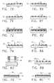
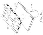
- FIGS. 13A-13C, 13 F- 13 Iare perspective views of some of the structural steps used to construct electrodes inside hollow microneedles.
- FIGS. 13D-13Eare magnified plan views of the individual electrode patterns used in the photolithography steps of FIGS. 13B and 13C.
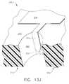
- FIG. 13Jis a perspective view in partial cross-section and magnified of a single hollow microneedle having an internal electrode, as seen in FIG. 13 I.
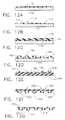
- FIG. 14is a plan view of a microneedle array that contains electrode bands.
- FIGS. 15A-15Lare diagrammatic cross-sectional views of structural steps used to fabricate sharp tipped microneedles.
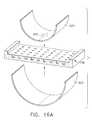
- FIGS. 16A-16Eare perspective views showing the structural steps utilized to manufacture convex or concave microneedles using flexible molds.
- FIG. 17is a perspective view of a solid microneedle having an external channel along its elongated side wall.
- FIG. 18is a top, elevational view of multiple solid microneedles each having two external channels along their elongated side wall.
- polymeric microneedlescan be fabricated by replica molding in which PDMS molds are prepared using a photoresist master.
- polymeric microneedlescan be made by replica molding in which PDMS molds are made utilizing a silicon wafer that is fabricated by deep reactive ion etching or any other etching technique known by those skilled in the art.
- the PDMS materialbecomes a negative replica which is used as a mold that can be later filled with a prepolymer material that will itself become an array of microneedles.
- Both solid and hollow microneedlescan be made by the techniques of the present invention.
- PDMSpolymethyl methacrylate
- PDMSTMis manufactured by Dow Corning Corporation of Midland, Mich.
- this materialis patterned by use of photolithography techniques, and the patterned structure is used to create the PDMS negative replica.
- the precise design for the transparency mask used in the photolithography proceduresutilizes a microfabrication method that is based on a rapid prototyping technique which uses design software and a high resolution printer; however, masks prepared using the traditional methodologies known by those skilled in the art can also be implemented using this process.
- the present inventionmakes good use of photolithography, generally using SU-8 photoresist materials, and a combination of replica molding using soft lithography, electroplating or microembossing processes. Such processes are less expensive and have quicker turnaround time (e.g., less than twenty-four hours) than those previously known in the art for the fabrication of microneedles.
- SU-8is used throughout this patent document in very many places as an example of photoresist material, it will be understood that other materials could instead be used in lieu of SU-8, which is a particular brand of photoresist manufactured by MicroChem Corporation of Newton, Mass.
- SU-8TMhas some particularly desirable characteristics, in that as a photoresist it can produce a film thickness greater than or equal to thirty (30) microns.
- the designerwishes to produce a photoresist film having a thickness less than 30 microns, then certainly other photoresist materials could be used.
- photoresist materials other than SU-8 that produce film thicknesses greater than 30 micronsmay be available, or may become available, and those could perhaps be advantageously used in the present invention.
- the present inventionnot only uses photolithography for patterning certain structures, but also uses “soft lithography” for creating structures in three dimensions using molds made of a polymer material or similar non-metallic material.
- the soft lithographyis a methodology in which all members involved share a common feature in that they use a patterned elastomer as the mask, stamp, or mold. (See, “Soft Lithography,” by Younan Xia and George M. Whitesides,” Angew. Chem. Int. Ed. 1998.37.550-575.)
- This elastomeric stamp or moldtransfers its pattern to the “moldable material” which can comprise flexible organic molecules or other materials, rather than rigid inorganic materials now commonly used in the fabrication of microelectronic systems.
- such soft lithography processesare utilized in almost every methodology for creating an array of microneedles.
- Silicon masters fabricated using conventional silicon micromachining technologiessuch as deep reaction ion etching, or structures prepared using LIGA processes, also can be employed for replica molding of microneedles. Such silicon masters will generally require more time in creating the replica molds as compared to the microfabrication methods of the present invention that create mold replicas using photoresist or PDMS (or similar) materials.
- microneedlescan be made of electrodepositable metals, thermoplastics, or polymers that cure using heat energy, light energy, or by the addition of an initiator under normal conditions.
- photolithography techniquesare used, then the light energy is generally used for both patterning and curing the materials, although the curing methodologies can certainly involve other types of energy sources than light.
- the replica moldcan often be made of PDMS material, which is formed into the appropriate shapes by use of a silicon or metallic structure that has been entirely formed to the proper shape, or a silicon wafer structure that has predetermined protrusions that are made of a photoresist material, in which the photoresist was patterned using photolithography techniques.
- PDMS mold negative replicaOnce the PDMS mold negative replica has been formed, it can be filled with a prepolymer or other type of moldable material, in which the prepolymer or other material becomes the actual array of microneedles. The prepolymer is then cured in a soft lithography process step.
- An alternative fabrication techniqueis to begin with a layer of photoresist material that is separated from a silicon wafer or other substrate material by a “sacrificial layer,” made of a material such as PDMS or silicon oxide.
- One fabrication techniqueis to place a first layer of photoresist that is cured without using a mask, and then placing a second layer of photoresist that is patterned using photolithography or other patterning techniques.
- the first photoresist layerlater becomes the substrate or base of a microneedle array, while the second layer of photoresist material later becomes the actual protrusions that create the microneedle structures, either solid or hollow.
- the sacrificial layeris then dissolved or otherwise decomposed, thereby separating the silicon wafer initial substrate from the microneedle array.
- the fabrication procedurescan be used to make either solid or hollow microneedles. If hollow microtubes are to be created from a silicon wafer having a photoresist top layer, then the top layer of photoresist is patterned as an array of hollow microtubes using photolithography techniques. After that has occurred, the “wafer/patterned photoresist” is silanized and coated with a PDMS material that is cured in a soft lithography process. Once the PDMS has been cured, it is separated from the original silicon wafer/substrate and patterned photoresist combination, thereby producing a negative replica comprising PDMS.
- the negative replicais then filled with a prepolymer material that is cured with electromagnetic energy or heat energy in a soft lithography process, and once cured the prepolymer is detached from the PDMS mold replica, thereby forming an array of hollow microneedles.
- the microneedlesmay not be completely hollow, as the through-holes only go so far into the photoresist material.
- these “microcups”can be opened by laser ablation, or some other type of microfabrication technique.
- An alternative methodology for creating hollow microneedles or “microtubes”is to begin with a silicon wafer or other substrate material, place a sacrificial layer on its top, and further place a layer of photoresist above that sacrificial layer. This first layer of photoresist is cured without using a mask, and then it is covered with a second layer of photoresist that is baked to dryness. An array of microneedles or “microtubes” is then formed in the second layer of photoresist by photolithography techniques. Once this has occurred, the sacrificial layer is dissolved or otherwise decomposed, thereby leaving behind an array of microneedles made of the photoresist material. At this point, the microneedles may not be completely hollow, as the through-holes only go so far into the photoresist material. Of course, these “microcups” can be opened by laser ablation, or some other type of microfabrication technique.
- hollow microtubes or microcupshave been formed on a silicon wafer or other substrate, they can be made more detachable in skin by an application of an acid along the base of the outer walls of the microneedles, to thereby etch away a small portion of the material at the base. This will make it more likely that the microneedles can easily detach from the main base or substrate of the microneedle array. This is useful in situations where the microneedles are used to penetrate the stratum corneum of skin, and then have the array base or substrate removed from the skin surface. The microneedles will break away from that substrate/base at that time, thereby leaving hollow microneedles within the stratum corneum. Such microneedles will stay embedded in the stratum corneum until the stratum corneum is renewed, thereby providing a location on the skin where liquids temporarily can be introduced or extracted.
- Break-away microneedlescan also be made by use of PDMS materials or other coatings that have poor adhesion with photopolymers as the substrate and a photoresist material that makes up the actual microneedles.
- Such photoresist hollow microneedleswould likely break away from the PDMS substrate/base of the microneedle array upon application into the stratum corneum of skin. This would then leave behind multiple such hollow microneedles in the stratum corneum once the array's base/substrate is removed.
- the present inventionalso provides procedures that can fabricate hollow microneedles using deposition techniques. Both metallic hollow microneedles and polymeric hollow microneedles can be constructed in such a manner.
- the metallic hollow microneedlesare made by creating a PDMS negative replica that is then electroplated onto the microneedle structure. This would typically produce “closed” microneedles, which could have their own usefulness, although in many cases the microneedles will be opened to create microtubes with through-holes by use of some type of polishing operation.
- Polymeric hollow microneedlescan be constructed using deposition techniques by creating a negative PDMS replica and electrodepositing a polymer on “posts” or other microneedle-type structures that are constructed from the PDMS. Once the polymer has been plated on the PDMS, the plated polymer is separated from the PDMS mold, thereby leaving behind multiple microneedle structures that have the form of “closed” microneedles. Such microneedles can be opened to create completely through-hole hollow microneedles by a polishing operation.
- the principles of the present inventioncan also be used to manufacture hollow microneedles using complimentary molds made of PDMS.
- two separate silicon wafersfor example, can be used as starting points in which each are coated with a layer of photoresist material.
- photolithography techniqueseach of these wafers has its photoresist layer patterned; in the first case holes are formed in the photoresist layer, and in the second case posts or other similar structures are formed in the photoresist. These patterns will be complimentary, as will be seen below.
- Both wafersare now silanized and coated with PDMS.
- the PDMSis cured, and once cured, the PDMS forms a negative replica that can be removed or detached from their respective silicon wafers.
- the photolithography stageforms both holes and “posts” that are complimentary to one another, and therefore, the two negative replicas made of PDMS are also complimentary.
- One of these negative replicasis turned upside down, a layer of prepolymer is then placed on top of that “turned-around” PDMS negative replica, and then the second negative replica is placed on top of the prepolymer, thereby sandwiching the prepolymer in place.
- the prepolymeris now cured and the two PDMS molds are detached, thereby leaving behind a separate polymer structure. If the shape formed “closed” hollow microneedles, then the closed end of these microneedles can be opened by use of some type of finishing or polishing procedure.
- a first layer of photoresistis placed on a silicon wafer or other substrate structure, and holes or other similar patterns are formed in the photoresist by photolithography techniques.
- a second layer of photoresistis then coated onto this structure, and using a second photolithography procedure, microneedle forms can be made, including hollow tube microneedles.
- This structureis now silanized, and a PDMS negative replica is formed based upon this pattern.
- the PDMSnow becomes a mold itself, and a polymer material can be placed onto the PDMS negative replica and cured or embossed, thereby forming an array of microneedle structures.
- microneedlesform “closed” hollow microneedles
- the closed endscan be removed by polishing or other type of finishing procedure. This would leave behind an array of hollow microneedles having through-holes. Polishing can be avoided by pressing a PDMS flat against the mold filled with prepolymer.
- the principles of the present inventioncan also be used to create microneedles having internal electrodes.
- Two different initial structuresare used to create the electrode-microneedle combinations.
- a polymer microneedle arrayis constructed according to one of the processes described above, in which the microneedles are hollow with through-holes.
- the other structureconsists of a silicon (or other material) substrate that has a layer of photoresist material applied and patterned using photolithography. This structure is then silanized and coated with PDMS, which is then cured. The cured PDMS layer is then separated from the photoresist-substrate structure, thereby becoming a mask that will be aligned with the hollow microneedles of the first structure.
- metalis vapor deposited on the inside of the microneedles in a pattern that will run through a portion of the length of the hollow microneedles along their inner cylindrical surfaces.
- Similar maskscould also be prepared using electroplating, electroless plating, electrochemical micromachining, silicon or polymer etching.
- the electrode-microneedle combinationcan be constructed so that each hollow microneedle has an electrode that is electrically isolated from each other such hollow microneedle.
- groups of microneedlescan be electrically connected together by use of electrode “bands” in which a first group of multiple microneedles are electrically connected to a “working electrode,” a second group of multiple microneedles are connected to a “reference electrode,” and finally a third group of multiple microneedles are electrically connected to a “counter electrode.”
- a reference electrodeis not needed in a two-electrode system and, depending upon the electrochemical cell design, microneedle arrays could be used on structures that consist of only one electrode type, such as a working electrode, counter electrode, or reference electrode. These unitary-type electrode structures could be combined in a two-electrode or a three-electrode device. Microneedles are so small in size, that the “electrode bands” might be more useful in certain applications, and the microneedles could be either solid or hollow.
- microneedles having a very sharp tipcan also be used to construct microneedles having a very sharp tip. This could be done by having multiple layers that are patterned one after the other, in which each pattern creates a cylindrical or elliptical opening such that each lower opening is smaller in size than the next adjacent higher opening. This will create a series of photoresist layers, for example, that taper down to a very small opening.
- a substratesuch as silicon
- a sacrificial layer of materialsuch as silicon oxide.
- the base material of the microneedle arraycan be made from a first structural material, while the microneedles themselves can be made of a second structural material.
- Thisallows design freedom to create hydrophobic-hydrophilic combinations and controlled adhesion of the needles to the base.
- Another alternative structureis to chemically modify the microneedles to change their properties, such as treatment of silicon microneedles with silanizing reagents to derivatize the surfaces.
- a further alternative structural treatmentis the use of a plasma treatment of epoxy or other polymeric microneedles that impart different surface properties (that would affect the hydrophobic or hydrophilic properties).
- the use of plasma treatment, or chemically modifying the microneedlescan occur at the molecular level, and such processes are commonly referred to as “surface modification” of structures.
- Another alternative constructionis to incorporate carbon fibers or other composite materials into epoxy microneedles or polymeric microneedles, as well as their substrates, in order to make the substrates and/or microneedles more rigid.
- composite materials or carbon fiberscould reinforce the microneedles themselves to make them more rigid.
- substratescould be made more flexible, including the use of micro channels and grooves in the substrate. It may be likely that the microneedles themselves are to remain rigid in such a structure.
- microneedlesare rigid enough to break skin, but still have a certain amount of flexibility. This could be used in situations where the microneedles are to penetrate the skin and be held in place for a relatively long period of time. This could be used for continuous monitoring and/or dispensing systems. It would be an advantage to provide such flexible microneedles that would be virtually unbreakable while being used in such circumstances.
- Another alternative constructionis to place a metal coating over the microneedles as a final outer layer.
- Several different processescan be used to coat microstructures with metal layers, including electroplating (or electrodeposition), electroless plating, sputtering, vapor deposition, and plasma deposition. It is possible to electroplate some alloys, metal oxides, polymers, and composite materials. Depending on the material that is electroplated, the plating solution can be aqueous or organic.
- Electroless platingcan be used to deposit metal, oxides, or polymers on virtually any kind of substrates.
- Sputteringcan only be used to deposit thin metal films (from angstroms to nanometers), although sputtering is a fast and inexpensive technique that is convenient to coat non-conductive samples with seed metal layers for a later step of electroplating.
- Vapor depositionis preferred over sputtering in the cases where microsmooth metal and oxide films are desired or when common metals do not adhere strongly to the substrates.
- the sampleare placed in a vacuum chamber where the metals are evaporated using resistive heating or an electron beam.
- the metal vaporsdeposit on the cold areas of the vacuum chamber, including the sample surface.
- the specimensare coated with a few angstroms of a metal adhesion layer prior to the deposition of the metal or oxide or interest.
- Plasma depositionis a technique that can be employed to deposit very thin films (having a thickness in the order of angstroms) of several kinds of materials on conductive or non-conductive substrates.
- this processtypically is slow and expensive. It is normally utilized to prepare films of materials that cannot be handled using the methodologies mentioned above.
- FIG. 1consists of FIGS. 1A-1F, and illustrates a process that can produce polydimethylsiloxane (PDMS) molds used in the fabrication of solid microneedles that are made of thermally light, or self-curable polymers or by embossing thermoplastics.
- PDMSpolydimethylsiloxane
- the first step in the microfabrication method of the present inventionis to spin-coat a layer that is about 20-200 microns in thickness of a photoresist compound (e.g., SU-8) on a silicon wafer, and baking to dryness at 90° C.
- a photoresist compounde.g., SU-8
- the silicon waferis at reference numeral 10
- the photoresistis at reference numeral 12 on FIG. 1 A.
- the photoresist filmis then patterned with posts 14 having a diameter in the range of 10-100 microns, using photolithography, as illustrated in FIG. 1 B.
- the waferis then silanized with an alkyl chlorosiloxane compound, then covered with PDMS and cured in an oven at about 60-70° C. for about two hours.
- This soft lithography stepis illustrated in FIG. 1C, where the layer of PDMS is at reference numeral 16 .
- the PDMS negative replicais detached manually from the silicon/SU-8 master, as illustrated by the negative replica 16 of FIG. 1 D. Naturally, this detachment operation can be automated.
- the PDMS structureis then filled under a vacuum with a photocurable polymer or a prepolymer material, such as epoxy known as UVO-110 under a vacuum.
- a photocurable polymer or a prepolymer materialsuch as epoxy known as UVO-110 under a vacuum.
- This structureis irradiated with ultraviolet light for two hours using a mercury lamp, or other ultraviolet light source to cure the prepolymer 18 , in a soft lithography process step.
- FIG. 1Ein which the prepolymer is at reference numeral 18 .
- the microneedle structureis separated from the mold, leaving a microneedle array 18 made of polymer as seen in FIG. 1 F.
- silicon microstructure array masters prepared using deep reactive ion etching (DRIE), or metallic microstructure array masters (prepared using, e.g., LIGA techniques)could be employed instead of the SU-8 photoresist masters to manufacture polymeric microneedles as shown in FIG. 1 .
- This alternative methodologyis illustrated in “FIG. 2 ,” which consists of FIGS. 2A-2E.
- the silicon microstructure array masteris illustrated at the reference numeral 20 .
- the microstructurecould be made of a metallic substance.
- the silicon structure 20is then silanized and covered with PDMS at 22 , as seen in FIG. 2 B. After being covered with the PDMS material, the structure is cured in an oven at about 60-70° C. for about two hours.
- the PDMS negative replicais detached from the silicon or metallic master 20 , leaving the negative replica structure 22 , as viewed in FIG. 2 C.
- the PDMS structure 22is then filled with a photocurable polymer at 24 , as seen in FIG. 2 D.
- This photocurable polymeris then exposed to a light source, such as an ultraviolet light source from a mercury lamp. This cures the polymer, and the microneedle apparatus is then separated, leaving the microneedle array 24 , as viewed in FIG. 2 E.
- a light sourcesuch as an ultraviolet light source from a mercury lamp.
- An example of an ultraviolet-curable polymeris a compound known as Uv-114, manufactured by Epoxy Technologies Inc.
- FIG. 3consists of FIGS. 3A-3E.
- An oxidized silicon wafer at 30includes a top layer of PDMS at 32 , which is coated with a layer of photoresist material at 34 , as viewed in FIG. 3 A.
- This structureis baked to dryness and cured with ultraviolet light to obtain a solid film of the cured photoresist material at 36 (see FIG. 3 B).
- An example of this photoresist materialis SU-8.
- FIG. 3An example of this photoresist material is SU-8.
- FIG. 3Bis coated again with photoresist, in this case a layer 38 in the range of 20-200 microns thick.
- This structureis baked to dryness at approximately 90° C., providing the structure of FIG. 3C in which the second layer of photoresist is illustrated at the reference numeral 38 .
- Microneedlesare formed in the second layer of photoresist 38 by a photolithography technique using a transparency mask patterned with dots having a diameter in the range of 20-100 microns. This provides the structure of FIG. 3D, in which solid microneedles at 40 are formed in an array-type structure.
- microneedle structure 40 of FIG. 3 Eis separated from the wafer by dissolving a “sacrificial layer” with an appropriate reagent, in which the PDMS layer 32 is decomposed with tetrabutylammonium fluoride (TBAF) and tetrahydrofuran, leaving behind the microneedle array structure 40 of FIG. 3 E.
- a “sacrificial layer”with an appropriate reagent, in which the PDMS layer 32 is decomposed with tetrabutylammonium fluoride (TBAF) and tetrahydrofuran, leaving behind the microneedle array structure 40 of FIG. 3 E.
- TBAFtetrabutylammonium fluoride
- FIG. 4An alternative methodology for generating a freestanding photoresist material microneedle array is described in connection with “FIG. 4 ,” which consists of FIGS. 4A-4E.
- an oxidized silicon wafer 30which includes a layer of silicon oxide at 42 , is coated with a layer of photoresist material 34 and baked to dryness.
- the photoresist layer 34is exposed without using a mask and cured, which is illustrated at the reference numeral 36 in FIG. 4 B.
- the wafer structureis then coated with a second layer of photoresist material at 38 and baked to dryness at about 90° C., which is illustrated in FIG. 4 C.
- Microneedle-like structuresare formed in the second photoresist layer by a photolithography procedure using a transparency mask that is patterned with dots having a general diameter in the range of 20-100 microns.
- Thisis the structure illustrated in FIG. 4D, in which the top layer 44 is the second photoresist layer that has microneedle structures protruding upwards in the figure.
- the wafer structureis then immersed in hydrofluoric acid (e.g., 10% solution) to detach the polymeric structure from the silicon substrate.
- hydrofluoric acide.g. 10% solution
- the silicon oxide layer 42acts as a sacrificial layer by dissolving or otherwise decomposing in the hydrofluoric acid.
- the array of solid microneedles in FIGS. 3E at 40 and 4 E at 44can be converted into “hollow” microneedles by various techniques.
- One well known techniqueis laser ablation, which would essentially bum holes through the centerline (or approximately near the centerline) of each of the cylindrical microneedle structures.
- One aspect of the present inventionis to create microneedle arrays that include individual microneedles that exhibit a “high aspect ratio.”
- the overall length of a microneedle divided by its overall widthis equal to the aspect ratio. If a microneedle is 200 microns in length, and its width (or diameter if it is circular) is 50 microns, then its aspect ratio is 4.0. It is desirable to use a relatively high aspect ratio of at least 3:1, although creating such structures can be difficult.
- microneedlesare so tiny in actual size (especially in the smaller widths or diameters) that it is not an easy task to make them sufficiently strong to penetrate the stratum corneum of skin without breaking. So there is a trade-off; one cannot merely make the microneedles “thicker” (or wider), because there needs to be some open area between each of the microneedles in the array to allow the tips of the microneedles to actually penetrate the outer skin layer.
- This aspect of the use of microneedlesis described in detail in a patent application that is assigned to The Procter & Gamble Company, under Ser. No. 09/328,947 which was filed on Jun. 9, 1999, and titled “Intracutaneous Microneedle Array Apparatus.” This patent application is incorporated herein by reference in its entirety.
- microneedlesAt the same time, one cannot merely make the microneedles shorter to decrease the chance of their being broken upon insertion into skin.
- the individual microneedlesshould be longer than the thickness of the stratum corneum, or they will not sufficiently increase the permeability of the skin to the fluid of interest.
- FIGS. 5 and 6Two different methodologies for fabricating hollow microneedles are illustrated in FIGS. 5 and 6, and are described immediately below.
- FIG. 5(which comprises FIGS. 5A-5F) starts with a silicon wafer at 50 with a top layer of photoresist at 52 (see FIG. 5 A).
- One preferred methodology for creating this structureis to use a spin-coating procedure to apply a layer of photoresist material that is in the range of 20-200 microns thick on the silicon wafer 50 .
- This structureis baked to dryness at approximately 90° C., and then the photoresist 52 is patterned with hollow cylinders by use of a photolithography procedure, which results in the structure of FIG. 5 B.
- the photoresist materialhas been formed into multiple hollow tubes at 54 , in which each of these hollow tubes comprises a hollow cylinder having a wall 58 and an open hollow space at 56 within these walls 58 .
- the structureis then silanized with an alkyl chlorosiloxane compound, then covered with PDMS under a vacuum, and cured in an oven in the range of 60-70° C. for approximately two hours in a soft lithography process step.
- Thisprovides the structure seen in FIG. 5C, in which the PDMS layer is designated by the reference numeral 60 .
- the PDMS moldis separated from the photoresist master, thereby providing the structure 60 by itself, as seen in FIG. 5 D. This structure 60 will be used to obtain plastic “microcups.”
- FIG. 5Ethe PDMS mold 60 has been inverted with respect to FIG. 5 D.
- This PDMS mold 60is now filled with a prepolymer material 62 , and this prepolymer is cured with some type of heat energy or with electromagnetic radiation, such as ultraviolet light in another soft lithography process step.
- the prepolymer material 62is detached from the mold 60 , thereby leaving behind the structure 62 as seen in FIG. 5 F.
- polymeric microneedlesare formed as part of the structure 62 , in which each of these microneedles has the form of a “microcup” 64 .
- These microcupsinclude an outer cylindrical wall 68 and a center open volume 66 .
- these microcupscould be made into “microtubes” or other type of hollow microneedle by use of laser ablation, or by some other technique, if desired.
- FIG. 5the hollow microneedles or microcups were formed using PDMS molds.
- photolithography of a photoresist mounted on a substrate covered with a sacrificial filmcould be utilized, as will now be discussed in reference to “FIG. 6 ,” which consists of FIGS. 6A-6E.
- a layer of photoresist material 74is applied, preferably by spin-coating. This is the structure illustrated in FIG. 6 A. This structure is then baked to dryness at approximately 90° C. If PDMS is used for layer 72 , it could have a thickness of approximately 100 microns, or if silicon oxide is used, its thickness could be much smaller, on the order of 500 nm.
- the structureAfter being baked, the structure has the appearance as illustrated in FIG. 6B, in which the silicon wafer 70 and intermediate layer 72 is topped by a cured or “baked” layer of photoresist at 76 .
- This structureis then coated again with a further layer of photoresist at 78 , as viewed in FIG. 6 C.
- This structureis then baked, and patterned with a transparency mask using photolithography techniques.
- Thisprovides the structure as viewed in FIG. 6D, in which multiple hollow structures 82 are formed as part of an overall photoresist layer 80 .
- These hollow structures 82are also in the form of “microcups,” similar to those disclosed in reference to FIG. 5 F.
- the microcups 82each have a cylindrical wall 86 , as well as a hollow volumetric space at 84 within the cylindrical walls 86 .
- This microneedle or microcup array structure 80can be readily detached from the substrate, thereby leaving behind the array structure as viewed in FIG. 6 E. This could involve dissolving the sacrificial layer 72 , which if the sacrificial layer consisted of PDMS would involve TBAF (tetrabutylammonium fluoride) in THF (tetrahydrofuran); if the sacrificial layer consisted of silicon dioxide, then the dissolving fluid would be 10% hydrofluoric acid.
- TBAFtetrabutylammonium fluoride
- THFtetrahydrofuran
- Wafers that have been coated with sacrificial layerscan also be used to fabricate hollow microtubes that can be easily detached from the base structure or substrate of the microneedle array, upon the application of small forces.
- Such detachable hollow microneedles or microtubescan be used to open momentary cavities across the stratum corneum of the skin. These cavities are not permanent, due to the natural shedding process of the stratum corneum.
- FIG. 7One methodology for constructing such detachable hollow microtubes is illustrated in “FIG. 7 .”
- “FIG. 7 ”consists of FIGS. 7A-7B and 7 X- 7 Z, but it will be understood that the first three steps of this procedure in FIGS. 7X-7Z involve the structures illustrated in FIGS. 3A, 3 B, and 3 C.
- FIG. 3Cinvolves a silicon wafer 30 , a layer 38 of PDMS material that is baked to dryness.
- solid microneedleswere formed using a photolithography process.
- hollow microtubeswill be formed, and these structures are indicated at the reference numeral 90 .
- each of these hollow microtubesconsist of a cylindrical wall portion 94 , which encompasses an open volume 92 .
- the microneedles fabricated on the PDMS filmi.e., layer 32
- do not need any type of treatment prior to skin penetrationbecause the adhesion between PDMS and most polymers is relatively weak. Therefore, the microneedles will fairly easily detach upon penetration into the stratum corneum.
- FIG. 7Bin which the microtubes 90 are shown in place in the stratum corneum layer 100 .
- the epidermis layer 102 and the dermis layer 104are also illustrated in FIG. 7B, which of course lie beneath the stratum corneum layer 100 .
- FIG. 8An alternative fabrication methodology would be to use a silicon wafer that has a silicon oxide layer 42 , such as that provided by the structure illustrated in FIG. 4 C.
- This alternative fabrication methodologyis illustrated in “FIG. 8 ,” which consists of FIGS. 8A-8D and 8 X- 8 Z. It will be understood that the first three process steps in FIGS. 8X-8Z involve structures having the appearance of FIGS. 4A, 4 B, and 4 C.
- FIG. 4Cincluded a silicon wafer 30 , a layer of silicon oxide 42 , an upper layer of cured photoresist 36 , and a second layer of photoresist at 38 that was baked to dryness.
- the photolithography processwas used to form solid microneedles.
- the transparency maskis used to create hollow microneedles or “microtubes” by the same type of photolithography process.
- the microtubes 90are very similar in appearance to those illustrated in FIG. 7 A.
- Each of the microtubeshas a cylindrical outer wall 94 that encompasses a hollow volumetric space 92 .
- FIG. 8Ban additional procedure of treating the “sacrificial layer” 42 with hydrogen fluoride (at 10%) for approximately two (2) to five (5) minutes will weaken the needle/substrate interface, as seen at the portion designated by the reference numeral 96 .
- the hydrogen fluoride treatmentwill tend to etch away a certain portion of the silicon oxide layer, and leave behind “break away” portions of the cylindrical walls that will facilitate the detachment of the hollow microtubes upon skin penetration.
- a magnified view of the resulting microtube 98 having the “weakened” (or “break-away”) area 96is provided on FIG. 8 D.
- One structure that has been successfully testedinvolves a silicon oxide layer that is approximately 500 nm in thickness, and covered with a photoresist material (e.g., SU-8) of about 20-200 microns that have been baked to dryness at 90° C. This will produce hollow microtubes or microneedles that have a length in the range of about 20-200 microns.
- a photoresist materiale.g., SU-8
- FIG. 8Cshows the final result, in which the “break-away” hollow microneedles or microtubes at 98 are embedded in the stratum corneum 100 .
- FIGS. 9 and 10illustrate some of the steps for two different methodologies of fabricating metallic hollow microneedles. “FIG. 9 ” consists of FIGS. 9A-9G while “FIG. 10 ” consists of FIGS. 10A-10G.
- FIG. 9Aillustrates a silicon wafer 110 that has had a photoresist layer spin-coated at 112 .
- An example of photoresist materialis SU-8, and the thickness of this material could be in the range of 20-200 microns.
- the photoresistis then patterned with cylindrical holes 116 using a photolithography process, thereby providing the structure in FIG. 9B in which the silicon wafer 110 is now topped by a photoresist layer 114 that has a plurality of such cylindrical holes 116 .
- These holescould have a diameter in the range of 20-100 microns, or virtually any other size, as desired for a particular application.
- This structureis now silanized and then covered with PDMS material that is cured for about two hours at approximately 60-70° C. in a soft lithography process step.
- the resulting structureis illustrated in FIG. 9C, in which the silicon wafer 110 and photoresist layer 114 are topped by the cured PDMS 118 .
- the PDMS negative replica 118is now removed or detached from the photoresist master, leaving behind the unitary structure 118 that is illustrated in FIG. 9 D.
- the PDMS mold negative replica 118is now coated with a metallic substance using sputtering or vapor deposition. This is illustrated in FIG. 9E, in which the PDMS material 118 is coated or plated with a metal layer at 120 .
- a metal layer at 120One example of this metal coating could be a layer of gold that is approximately 50 angstroms in thickness.
- Another exampleis to use a layer of nickel, copper, gold, platinum, or silver having a thickness in the range of 10-30 microns, by use of an electroplating procedure on the previously coated gold/PDMS structure. This will form an array of metallic needles that can be isolated by dissolving the PDMS layer in a 1 M solution of TBAF in THF, thereby leaving the unitary structure 120 that is illustrated in FIG. 9 F.
- the structure 120is the separate metal layer that has been detached from the PDMS mold.
- This structure 120includes an array of protrusions at 122 , each of which will become the basis for a hollow microneedle or microtube.
- the microneedles 122are essentially “closed” and have the form of “microcups” in essence, when viewed from above. Of course, when viewed from below, these closed microneedles 122 essentially act as liquid tight microneedles that have the appearance of solid microneedles.
- tubular microneedles 122are now “opened” by polishing the closed ends by one of several possible techniques, thereby leaving behind an array of hollow microneedles in a unitary array structure 124 that is illustrated in FIG. 9 G.
- Each of the hollow microneedles or “microtubes” 122includes a cylindrical wall 128 that surrounds a hollow volumetric space 126 that, in this illustrated embodiment, supplies a tubular passageway or through-hole from one surface of the unitary structure 124 to the opposite side of that same structure.
- the polishing technique described abovecould be as simple as using sandpaper on the surface where the closed end 122 existed in FIG. 9F, or it could be some type of milling or grinding operation, or finally some non-mechanical technique could be used, such as a laser beam to burn away or vaporize the closed end by laser ablation.
- the microneedle arrayscould be separated by hand from the PDMS molds and the metallic structures could be synthesized using electroless plating techniques.
- the moldscould be reused if the structures are disconnected by hand.
- the polishing stepcould be avoided if the tips of the PDMS/gold posts (at 122 ) were earlier stamped with a non-conductive material such as thiol monolayer or a polymer, or were peeled off using adhesive tape.
- FIG. 10An alternative technique for creating metallic microneedles is illustrated in FIG. 10 .
- a silicon wafer 110 that has had a photoresist layer spin-coated at 112is illustrated (similar to FIG. 9 A).
- An example of photoresist materialis SU-8, and the thickness of this material could be in the range of 20-200 microns.
- the photoresistis then patterned with cylindrical holes 116 using a photolithography process, thereby providing the structure in FIG. 10B in which the silicon wafer 110 is now topped by a photoresist layer 114 that has a plurality of such cylindrical holes 116 .
- These holescould have a diameter in the range of 20-100 microns, or virtually any other size, as desired for a particular application.
- This structureis now silanized and then covered with PDMS material that is cured for about two hours at approximately 60-70° C. in a soft lithography process step.
- the resulting structureis illustrated in FIG. 10C, in which the silicon wafer 110 and photoresist layer 114 are topped by the cured PDMS 118 .
- the PDMS negative replica 118is now removed or detached from the photoresist master, leaving behind the unitary structure 118 that is illustrated in FIG. 10 D.
- the PDMS negative replica 118 of FIG. 10Dis now used in a vapor deposition procedure, and then a procedure where polymer is electroplated.
- the vapor depositioncould involve chromium or gold, for example. This would lead to the structure 118 of FIG. 10E, in which the plated polymer layer is at 130 .
- This particular procedurecould also be modified to construct tapered microneedles by overexposing the photoresist master and then fabricate plastic hollow microneedles by electrodepositing the polymers, such as the layer 130 of plated polymer material.
- polymer materials that can be electroplatedinclude POWECRON® acrylic epoxies (manufactured by PPG Industrial Coatings of Pittsburgh, Pa.), and EAGLE 2100® (manufactured by The Shipley Company of Marlboro, Mass.
- the polymer microneedlesare separated from the PDMS mold, thereby leaving behind the unitary structure 130 of FIG. 10 F. At this point, the projections that will eventually become tubular microneedles are “closed,” as viewed at 132 on FIG. 10 F. Therefore, a procedure is performed to “open” the microneedles, by use of some type of polishing technique, similar to that described above in reference to FIG. 9 G.
- Thisprovides the structure 134 illustrated in FIG. 10 G.
- the microneedle array structure 134includes hollow microneedles or “microtubes,” each of which consists of a cylindrical wall 138 that encompasses an open volumetric space 136 that extends from one surface to the other of the microneedle array 134 .
- FIG. 11illustrates a fabrication technique by which microneedles are constructed by curing polymers that are sandwiched between complimentary PDMS structures.
- FIG. 11consists of FIGS. 11A-11K, and beginning at FIG. 11A a silicon wafer 140 is spin-coated with a photoresist material 142 , such as SU-8. A second wafer 150 is also spin-coated with a photoresist compound 152 , as illustrated in FIG. 11 E.
- the photoresist layer 142 thicknessis approximately 175 microns for the wafer 140 of FIG. 11A, while the thickness of the photoresist layer 152 is approximately 200 microns on FIG. 11 E.
- An array of posts 154are formed from the photoresist 152 by use of patterning and photolithography techniques, and these posts have a separation of approximately 300 microns with a height of approximately 200 microns and a diameter somewhat less than 50 microns. See FIG. 11 F.
- both wafersare silanized, covered with PDMS or an equivalent material, and cured at approximately 60° C. for about two hours using soft lithography.
- Thisprovides the structures illustrated in FIGS. 11C and 11G, in which the PDMS layer 148 protrudes into the “hole” spaces 146 that are between the photoresist structures 144 , and the PDMS layer 156 on FIG. 11G, which surrounds the post 154 .
- the specimensare now cooled to room temperature, and the PDMS replicas are detached from the wafers, thereby providing the structures 148 and 156 , as illustrated in FIGS. 11D and 11H, respectively.
- One of these replica structures(preferably the structure 156 having the “holes”) is now coated with a relatively thin layer of a prepolymer material, such as polyurethane (PU), epoxy, polymethyl methacrylate (PMMA), bone suturing materials, dental polymers, or other similar prepolymer compound.
- PUpolyurethane
- PMMApolymethyl methacrylate
- the two structures 148 and 156are now aligned, in which the posts now resident in the structure 148 are aligned with the “holes” resident in the structure 156 . The result is illustrated in FIG.
- replica structure having “posts” 148is fitted atop the replica structure having the “holes” at 156 , and in which the above prepolymer material 160 is placed between these two replica structures 148 and 156 . Once they are aligned, they are pressed, or held together, and cured as appropriate, using heat energy or perhaps electromagnetic energy, such as ultraviolet light or visible light.
- the two PDMS mold replicas 148 and 156are now separated and the now cured polymer material 160 is separated from both of these mold replicas.
- These posts/protrusions 162are not solid, but are hollow, and have a form somewhat similar to a “microcup” as described above. As viewed from above in FIG. 11J, these protrusions would have the appearance of microcups, although when viewed from below, they would have the appearance of solid posts or microneedles.
- microneedles or microcupsThe purpose of this structure is not necessarily to create solid microneedles or microcups, and therefore, the closed ends at 162 of these protrusions are opened by some type of polishing procedure, thereby forming hollow microneedles or microtubes.
- These microneedles/microtubeshave cylindrical walls at 168 (see FIG. 11 K), and the walls 168 surround an empty volumetric space, as illustrated at 166 .
- the polishing procedurecould be simply the use of sandpaper, or a more sophisticated or automated procedure using a milling machine or a grinder, for example.
- the mold material 156 of FIG. 11Gcan be made of a material that has flexibility characteristics. Such a flexible mold can then be used to form microneedle arrays that are convex or concave in overall shape (i.e., the shape of their substrate).
- FIG. 16(which comprises FIGS. 16 A- 16 E), the original rectangular shape of the mold 156 is illustrated in FIG. 16A, along with a top mold plate 500 that is convex and a bottom mold plate 502 that is concave.
- the two mold plates 500 and 502are pressed against the flexible mold 156 , which itself takes the overall shape of a concave structure (as seen from above in this view).
- An open chamber at 504is thereby created between the top microstructure portions of the mold and the bottom surface of the top mold plate 500 .
- a hole 506 in the top mold plate 500can be used to place fluidic material (such as a molten plastic or a prepolymer material) into this chamber 504 .
- the chamber 504is now filled with a prepolymer material, such as polyurethane (PU), epoxy, polymethyl methacrylate (PMMA), bone suturing materials, dental polymers, or other similar prepolymer compound.
- PUpolyurethane
- PMMApolymethyl methacrylate
- the prepolymer materialis cured as appropriate, using heat energy or perhaps electromagnetic energy, such as ultraviolet light or visible light (one of the mold halves would have to be transparent to the particular wavelength if curing via light). This is the configuration viewed in FIG. 16 C.
- the mold plates 500 and 502are separated to release the cured polymer material, which has now become a convex microneedle array 510 .
- the individual microneedlesare designated by the reference numeral 512
- the semicircular substrate surface between microneedlesis designated by the reference number 514 .
- the “inner” surface 516 of the substrateis essentially concave, and could be used to form a reservoir to hold a liquid, if desired.
- the mold plates 500 and 502are made in the opposite shapes—i.e., if the top mold plate 500 was made in a concave shape and the bottom mold plate was made in a convex shape—then the resulting microneedle array would also be in the opposite shape, i.e., an overall concave shape.
- the individual microneedlesare designated by the reference numeral 522 , while the semi-circular substrate surface between microneedles is designated by the reference number 524 .
- the “outer” surface 526 of the substrateis essentially convex.
- a single microstructure mold 156can be used to manufacture microneedle arrays that are of various circular arcuate aspects.
- two different convex shapescan be manufactured from the single flexible mold 156 , simply by using two different angled plates for the top and bottom plates 500 and 502 .
- concave shaped microneedlescan also be made from the same flexible mold 156 , by use of two opposite shaped top and bottom plates (not shown).
- Polymeric hollow microneedlescan be fabricated using multilayer photoresist masters, as illustrated in “FIG. 12 ,” which consists of FIGS. 12A-12G.
- a film 172 of a photoresist materialsuch as SU-8 is spin-coated on a silicon wafer 170 , then baked to dryness at about 90° C.
- the thickness of the photoresistcould be in the range of 10-100 microns.
- This photoresist film 172is then patterned with cylindrical holes by use of photolithography, thereby resulting in an array of holes having a diameter of about 10-100 microns, as illustrated in FIG. 12 B.
- the holesare represented at the reference numerals 176 , while the remaining photoresist film is represented at 174 , which bounds these holes 176 .
- This patterned wafer structureis now coated again with a second layer of photoresist 176 , having a thickness of about 10-200 microns, or perhaps thicker if desired, resulting in the structure illustrated in FIG. 12 C.
- the photoresist layer 176is now patterned with hollow cylinders that are centered on the holes of the bottom layer (originally the film layer 172 ) using photolithography techniques.
- This photoresist structureis now silanized, covered with polydimethylsiloxane (PDMS) under a vacuum, and cured for about two hours in the range of 60-70° C.
- PDMSpolydimethylsiloxane
- FIG. 12Dthe final photoresist material has the form of an array of hollow microneedles, and given the overall designation 180 .
- Each of the microneedleshas an outer cylindrical wall at 184 , which encompasses a hollow cylindrical volume 182 .
- the PDMS material 180is detached from the silicon/photoresist master at room temperature, and now becomes a mold itself, which is filled with a prepolymer such as polyurethane (PU), epoxy, polymethyl methacrylate (PMMA), bone suturing materials, or dental polymers.
- PUpolyurethane
- PMMApolymethyl methacrylate
- cylindrical “posts” at 192are formed, which are surrounded by open areas 194 , which become a mold replica for forming microneedles that are hollow and cylindrical.
- the PDMS mold replicaalso has relatively flat surfaces at 196 that will become the substrate substantially flat surfaces between microneedle positions, and also has a final “bottom” surface (as viewed on FIG. 12E) at 198 that represents the deepest portion of the cylindrical open areas 194 .
- FIG. 12Hprovides a perspective view of this structure 190 , in which the relatively flat surface 196 represents the largest surface area as seen in this view.
- the cylindrical posts that protrude the farthestare designated at the reference numerals 192 , which have the cylindrical outer channels 194 with a bottom surface at 198 .
- embossing polymeris now placed on top of this surface, which will become the actual microneedle structure after the embossing procedure has been completed.
- the embossing polymerwould be squeezed against the PDMS mold replica 190 , although that may not be necessary in certain applications or by use of certain materials. This results in a microneedle array structure 200 , as illustrated in FIG. 12 F.
- a prepolymer materialcould be placed against the replica mold structure 190 and cured as appropriate (e.g., by use of heat energy or electromagnetic energy, such as visible light or ultraviolet light) in a soft lithography process; and after curing the microneedle array is separated from the mold 190 . This also results in a microneedle array structure 200 , as illustrated in FIG. 12 F.
- the microneedle array structure 200consists of multiple microneedle structures 202 , each having a cylindrical wall at 206 , which encompasses a cylindrical volumetric space at 204 . These microneedles are “closed” at this point, and take the overall form of “microcups.” The closed end portion of the microneedles is formed by the surface 208 of the array structure 200 .
- the closed portion 208can be removed from the array structure, which then provides the structure 210 illustrated on FIG. 12 G.
- These hollow microneedles or microtubesare indicated at the reference numeral 212 , and have outer cylindrical walls 216 which encompass a through-hole of an open cylindrical shape at 214 .
- the softening point of the polymer to be embossedshould be less than about 400° C. to avoid any significant deformation of the PDMS microstructures of the mold piece 190 .
- the moldwas instead made of a metallic material, then a much higher temperature embossing procedure and material could be used.
- the mold structure 190 on FIG. 12Ecan also be used to directly create hollow microneedles without the need for a milling or grinding procedure to remove the closed portion 208 , as seen on FIG. 12 F.
- the surface of the mold structure 190is covered with an embossing polymer material at 220 , and is squeezed under pressure by a top plate (or top mold half) 230 .
- the embossing polymer materialis allowed to harden or cure before the top mold half 230 is removed.
- Hollow cylindrical structuresare thereby formed in the embossing polymer material 220 , in which the walls of the cylinders are indicated at 222 , and the internal openings at 224 .
- FIG. 12Jillustrates the molded material after the top mold half 230 is removed.
- the new structure 220continues to exhibit cylindrical openings which are now through-holes at 224 , each such hole having a cylindrical wall structure at 222 .
- the holes 224were directly formed during the molding process because the top mold half 230 removed all excess embossable material from the top of the posts 192 of the mold structure 190 (see FIG. 12 I).
- through-holes and associated wall structurescould have a shape other than cylindrical without departing from the principles of the present invention.
- these hollow microneedles formed in the microneedle array structure 220instead could be elliptical, square, rectangular, or edged in form.
- Macroscale glucose electrochemical sensorsconsisting of two electrodes immersed in a conducting media composed of glucose oxidase, electrolytes, and hydrogel are among the most reliable sugar detectors available.
- glucose oxidaseconverts sugar to carbon dioxide and hydrogen, and an electrical signal is generated by the catalytic oxidation of hydrogen on the surface of a platinum electrode.
- Microneedle devicesthat include electrodes can be used as electrochemical sensors, and also they can be used for iontophoretic or electrophoretic delivery of drugs in interstitial fluids. Fabrication techniques to create electrodes that are integrated with the microneedle devices is described in detail below. Procedures for the construction of such microelectrodes on the surface of metallic or polymeric microneedles is disclosed using vapor deposition techniques.
- FIG. 13illustrates the fabrication processes and structural designs of such microelectrodes in microneedle structures, and consists of FIGS. 13A-13J.
- a silicon wafer 300has a spin-coating of photoresist 302 , which could be SU-8 photoresist having a thickness of approximately 50 microns.
- the photoresistis patterned with a structure illustrated in FIG. 13 D.
- FIG. 13DOne specific design is illustrated in FIG. 13D, in which the photoresist at 304 has dimensions provided on FIG. 13, and which appears on FIG. 13B as an array of such patterned designs.
- This patterning procedurepreferably involves photolithography, after which the structure is silanized. After that has occurred, the patterned wafer is covered with PDMS, pressed against a flat surface such as a glass slide, then cured at about 60° C. in a soft lithography process step.
- the PDMS membraneis illustrated in FIG. 13C after it has been removed from the wafer, and is designated generally by the reference numeral 306 .
- a single structure having this shapeis illustrated in FIG. 13E, in which the PDMS membrane 306 has an open area of a shape as illustrated at 308 .
- the structure 306represents holes or openings 308 in the PDMS membrane that will be used as a mask during a metal vapor deposition procedure.
- the longitudinal portion 316 of this opening 308in the relative center area of the pattern, is designed to form two microelectrodes inside each microneedle.
- the larger rectangular segments 318 of the pattern 308are utilized to construct electrically conductive pads 304 that will connect the microelectrodes to leads of an electrochemical analyzer.
- each of the pads 304will have dimensions of about 300 microns ⁇ 700 microns, and the longitudinal portion is represented by a rectangular shape 316 having dimensions of about 25 microns by 300 microns.
- An array 310 of polymeric or metallic microneedlesis prepared, and forms a structure as illustrated in FIG. 13F, by which microneedles 312 protrude from one surface of the array structure or substrate 310 .
- the microneedlesare metallic, they can be prepared using the fabrication techniques as described in reference to either FIG. 9 or 10 . If metallic microneedles are utilized, a thin film (of approximately 5-10 microns in thickness) of an insulating polymer is electroplated on the surfaces of this array 310 , thereby providing a structure as illustrated in FIG. 13G which is coated by an insulative layer of material. This will lead to a layer of insulative coating at 314 on the microneedles themselves.
- the microneedle array structure 310consists of an insulative material, then no additional polymer layer is required.
- the cured PDMS pattern 306is now placed upon the planar face of the microneedle structure 310 and the linear or longitudinal center portions 316 of each of the patterns 308 are aligned with each of the microneedle structures 314 .
- a metal vapor deposition procedurecan commence, while the structures are held in place by some type of clamp, tape, or temporary adhesive.
- a layer of metalsuch as gold or platinum, is then vapor deposited on the membrane/microneedle structure in a thermal evaporator, after which the PDMS mask 306 is detached from the microneedles, thereby forming a microneedle array structure 330 , as illustrated in FIG. 131 . While in the thermal evaporator, the samples are held at about 30-45° C. with respect to the metal source to ensure the deposition of metal inside the microneedles.
- the needlesare filled with the conducting media described above (e.g., hydrogel, electrolytes, or glucose oxidase) before they are used as glucose sensors.
- Each of the resulting microneedles 314protrudes from the planar substrate 310 , and each of these hollow microneedles 314 includes an electrode structure 320 that runs at least part way down the inside cylindrical wall surface 322 of the microneedles 314 .
- the electrode structure 320is electrically connected to a pad 306 , as illustrated in FIG. 131 .
- FIG. 13JA more detailed view of this structure 330 is provided in FIG. 13J, by which the microneedle array 330 includes an upper planar surface or substrate 310 , an electrically conductive pad 306 , an electrode 320 that is both connected to the pad 306 and runs down the inside surface of the cylindrical wall 322 that forms the inner hollow surface of the microneedle itself.
- the fabrication of a PDMS mask and the vapor deposition of metallic materialis not necessary if the polymer to be electroplated is a photoresist.
- the electrodes and padscan be constructed by use of photolithography techniques. Not only are very small electrode structures able to be constructed by photolithography, but in addition larger electrode structures can be formed, also using photolithography. Such an example is illustrated in FIG. 14 .
- electrode “bands”are formed on a microneedle array structure, rather than using independent electrode systems for each microneedle as illustrated in FIG. 131 .
- a large number of microneedles 352are formed on a microneedle array 350 .
- the top planar surface 354shows that different materials can be applied thereto.
- a “working electrode” 360can be formed on one portion of this structure 350 , and can encompass a number of the microneedles 352 , including the inner cylindrical hollow surfaces of these microneedles 352 .
- a “counter electrode” 364can be formed in a different area, and can also encompass many such microneedle structures 352 .
- a “reference electrode” 362can be formed using a third set of microneedles 352 .
- Each electrode areais electrically conductive between each of its individual microneedles 352 by an electrically conductive metallic surface along the top of the substrate at 354 .
- Such electrode bandscould alternatively be formed on the opposite side of the microneedle array. In other words, electrode bands could be formed on either the top or the bottom of the microneedle array 350 when hollow microneedles are used.
- solid microneedlescould be used at 352 , if desired.
- the solid structure 352could have the form of cylindrical posts that are coated by electrically conductive metal within the various bands 360 , 362 , or 364 . If the microneedles started as hollow structures, their inner diameters could be filled (or at least plugged) by the metal of the electrode bands 360 , 362 , or 364 .
- Glucose sensorscould also be formed using polymeric microneedles, as mentioned above.
- the polymeric microneedlescan be formed in the same manner as metallic microneedles, in which the initial specimen is covered with a PDMS mask prepared as described in reference to FIGS. 13A-13C.
- the electrodescan then be formed by metal vapor deposition in a thermal evaporator, or perhaps in a sputtering machine.
- FIG. 15illustrates some of the fabrication steps in such a procedure, in which “FIG. 15 ” consists of FIGS. 15A-15L.
- the wafer structureis coated with a layer of photoresist 404 .
- This layer 404is baked to dryness and then patterned using a transparency mask and an electromagnetic light source (such as an ultraviolet light source) so as to create locally a relatively small cylindrical hole, as seen at 410 in FIG. 15 B.
- an electromagnetic light sourcesuch as an ultraviolet light source
- a second layer of photoresist material 420is now placed atop the structure, as viewed in FIG. 15 C.
- this photoresist 420has been baked to dryness, it is patterned using ultraviolet light and a transparency mask to create locally another cylindrical opening that is somewhat larger than the first one 410 .
- This second cylindrical openingis designated by the reference numeral 426 on FIG. 15D, and it can be seen as separating the photoresist material 420 into two halves, 422 and 424 . It will be understood that this FIG.
- 15Dis a cut-away view, and the opening 426 is actually the further half (from the observer) of a cylindrical inner wall, and therefore, the two “halves” 422 and 424 still make up a single layer of photoresist material that has certain openings, such as the one at 426 .
- the next step after this second photolithography stepis to again place a further layer of photoresist material 430 atop the structure, thereby arriving at the structure illustrated on FIG. 15 E.
- this new layer of photoresist at 430has been baked to dryness, it is patterned using a light source and a transparency mask to create locally a somewhat larger cylindrical hole, as seen at 436 on FIG. 15 F.
- the photoresist layer 430is now illustrated as consisting of two halves at 432 and 434 , which are indeed a single layer.
- photoresist layer 440is much thicker than any of the earlier photoresist layers 404 , 420 , or 430 .
- the photoresist layer 440After the photoresist layer 440 has been baked to dryness, it is patterned using ultraviolet light and a transparency mask to create locally a still larger cylindrical hole, as seen at 446 on FIG. 15 H.
- the photoresist layer 440is now shown in two halves at 442 and 444 . It will be understood that certainly more than three intermediate layers of photoresist material could be used to create a mold form, as compared to that shown in FIG. 15 H.
- the mold structurehas been separated from the silicon wafer 400 by dissolving or otherwise decomposing the sacrificial layer 402 with an appropriate reagent.
- PDMScan be decomposed with TBAF, and silicon oxide or silicon dioxide can be immersed in hydrofluoric acid to cause the detachment.
- FIG. 15Jshows several of the holes 446 as part of an array of such holes in the total mold structure 450 .
- FIG. 15Kshows an arrangement where a plastic structure generally designated at the reference numeral 460 is placed between two mold halves 470 and 472 , which act as pressure bases, and also retain the plastic material 460 within the mold cavities that are available in contact with the patterned mold 450 . As can be seen in FIG. 15K, the plastic material 460 will flow into the shaped holes 446 that were created in this mold structure 450 .
- array 460includes multiple “sharp” microneedles 462 , as viewed in FIG. 15 L. As noted above, these “sharp tip” microneedles could be of various sizes and shapes, and certainly could be created from more than three stages of photoresist layers being patterned by use of photolithography techniques, without departing from the principles of the present invention.
- microneedles described aboveOne optional variant in the microneedles described above is to create a structure in which the base material is different from the microneedle structure material, which allows the designer freedom to create hydrophobic-hydrophilic combinations.
- examples of such different types of materialsare as follows: glass, mica, Teflon®, and metalized surfaces.
- microneedle structures described abovecan be of any length or width, or any inner diameter for hollow microneedles or microcups, without departing from the principles of the present invention. Certain exemplary dimensions have been disclosed above, but these are only examples of prototypical units. It will also be understood that the microneedles (both solid and hollow) could be constructed of various shapes other than cylinders, such as elliptical profiles, or “edged” microneedles, such as disclosed in a patent application that is assigned to The Procter & Gamble Company, under Ser. No. 09/580,780) which was filed on May 26, 2000, and titled “Intracutaneous Edged Microneedle Apparatus.” This patent application is incorporated herein by reference in its entirety.
- the chemical compounds disclosed aboveare exemplary for certain prototypical microneedles, and as such are quite useful, but at the same time other compounds might easily be employed without departing from the principles of the present invention.
- the substratedoes not always need to be silicon, and the sacrificial layer is not always required to be either PDMS or silicon oxide.
- PDMSpolymethyl methacrylate
- microneedle structures described aboveis to change their properties by a “surface modification” treatment which allows a coating to occur at the molecular level.
- the silicon needlescan be silanized with reagents to derivatize the surfaces. Typically, such coating would occur after the microneedles are already formed.
- Yet another alternative embodimentwould be a plasma treatment of epoxy or other types of polymeric microneedles to impart different surface properties. Again, such treatment would typically occur after the microneedles have been formed. One such different surface properties could be to impart hydrophobic/hydrophilic properties to the microneedles.
- Still another alternative embodiment of the microneedles of the present inventionis to incorporate carbon fibers or other composite materials into epoxy or polymeric needles and perhaps the substrate.
- the use of harder materialscould reinforce the polymeric needles and make them more rigid.
- One examplewould be to add carbon fibers or composite materials into a photoresist compound, such as that illustrated in FIG. 3A at 34 . This would lead to the microneedles at the microneedle array 40 in FIG. 3D to be more rigid.
- the entire microneedle structurecould be hardened, if desired, by incorporating carbon fibers or other composite materials into all of the materials used to manufacture the structure, including the base or substrate.
- the substrate materials utilized in creating the microneedles of the present inventioncould be made more flexible, although it normally would be preferred to keep the microneedles themselves as a rigid structure.
- One methodology for creating substrates that are more flexibleis to add microchannels and grooves to the substrate, thereby making the fairly rigid material have some “bendability” while not being prone to fracture.
- Another alternative “flexible” embodimentis to create more flexible microneedles themselves, in which the microneedle structures would be sufficiently rigid to break the skin, but still have some flexibility that would be quite useful for continuous sensing and dispensing systems. This would be the opposite of the break-away microneedles disclosed above, for example in FIGS. 8B and 8C.
- These flexible microneedleswould be achieved by using materials such as elastomers and polyurethanes that are moldable or embossable. Examples of such elastomers are silicones.
- Yet another alternative “flexible” embodimentis to create a microneedle structure in which the entire structure is at least somewhat flexible, although the flexibility properties of the needles could be different than the flexibility properties of the base.
- the needles, or at least their tipsare made of a first material (having a first flexibility or elasticity property) and the base/substrate is made of a second material (having a second flexibility or elasticity property).
- the base/substratecould be made of nylon while the microneedles are made of silicone or polyurethane, thereby providing a microneedle array that has a barely flexible base/substrate but a much more flexible set of needles.
- a further alternative embodiment for the microneedles of the present inventionis to place a final outer layer of a metal coating over the microneedle structures.
- thiswould have the appearance as viewed in FIG. 9E, which illustrates plated metal over a PDMS replica that itself could become a microneedle array.
- Such a structurehas the advantage of fairly quick manufacturing, while remaining accurate at the microstructure level and while having the surface properties of a structure formed entirely from metal.
- the thickness of the outer metal coatingcan be controlled by a vapor deposition or electroplating process.
- electroplatingor electrodeposition
- electroless platinge.g., gold
- sputteringe.g., tungsten
- vapor depositione.g., tungsten
- plasma depositione
- the plating solutioncan be aqueous (e.g., Ni, Cu, Ag, Au, Pb, Sn, or Pt) or organic (e.g., polymers, Al, or titanium oxides) and may contain stabilizers, brighteners, and wetting agents.
- electroplatingallows the formation of crystalline films as thick as 1-2 millimeters. If the sample to be electroplated is not electrically conductive, it must be coated with a thin film of a conductive material (e.g. metals or conductive polymers) prior to immersion in the electrochemical cell.
- Electroless platingcan be used to deposit metal, oxides, or polymers on virtually any kind of substrates.
- the sampleis cleaned using organic solvents (e.g., acetone or methanol) and/or mineral acids (e.g., hydrofluoric or nitric acid), activated for metal deposition using a metallization catalyst (e.g., palladium chloride), and immersed in a solution including electron donor species (e.g., phosphate ions) and the material that is going to be plated.
- a metallization catalyste.g., palladium chloride
- the thickness of the electroless plated filmscan range from a several angstroms to a few millimeters and is affected by the pH of the plating solution, time of reaction, and concentration of the chemicals involved in the deposition process.
- Sputteringcan only be used to deposit thin metal films (from angstroms to nanometers) on either conductive or non-conductive substrates.
- gas ionse.g., Ar
- a metal sourcee.g., Au, Pt, Cr, Ag, or Cu
- Sputteringis a fast (e.g., taking only a few minutes) and inexpensive technique that is convenient to coat non-conductive samples with seed metal layers for a later step of electroplating, including the fabrication of microelectrodes (employing a mask, such as the mask 306 in FIG. 13 H), provided that there is good adhesion between the metal film and the substrate.
- Vapor depositionis preferred over sputtering in the cases where microsmooth metal and oxide films are desired (having a coating thickness on the order of angstroms or nanometers) or when common metals (e.g., Au, Ag, Al, or Cu) do not adhere strongly to the substrates.
- the sampleare placed in a vacuum chamber where the metals are evaporated using resistive heating or an electron beam.
- the metal vaporsdeposit on the cold areas of the vacuum chamber, including the sample surface.
- the specimensare coated with a few angstroms of a metal adhesion layer (e.g., Cr or Ti) prior to the deposition of the metal or oxide or interest. This process is generally completed in one or two hours and is employed for the fabrication of electrodes, seed layers for electroplating processes, and the deposition of thin layers of metal on three dimensional samples (in which the sample can be rotated at an angle in the vacuum chamber).
- a metal adhesion layere.g., Cr or Ti
- Plasma depositionis a technique that can be employed to deposit very thin films (having a thickness in the order of angstroms) of several kinds of materials (e.g., organic compounds, polymers, oxides, or metal precursors) on conductive or non-conductive substrates. This process is slow and expensive. It is normally utilized to prepare films of materials that cannot be handled using the methodologies mentioned above.
- materialse.g., organic compounds, polymers, oxides, or metal precursors
- Solid microneedlescan be manufactured with external channels running along one or more sides of the elongated walls.
- FIG. 17illustrates a solid microneedle 600 that has a elongated side wall 610 and a top surface 612 at its tip.
- the length of the microneedleis designated by the dimension line 614 , which could be in the range of 100-500 microns.
- An external channel 620is formed in one side of the wall 610 .
- the channel 620is substantially rectangular in profile in this view, and could have dimensions (at 622 and 624 , respectively) of about 10 microns by 10 microns. Of course, the channel 620 could be of other dimensions, if desired. Channels can also be made to taper so as to increase capillary driving forces.
- the external channel 620is preferably in communication with another channel 632 that is in the base structure 630 of the microneedle array.
- This base channel 632could be used to transport interstitial fluid, for example, to a sensor device 640 .
- This sensor devicecould be electrochemical or optical in nature, or perhaps could use a different principle of operation.
- Groups of solid microneedles having external channelscould be formed of a single microneedle array.
- four such solid microneedlesare illustrated at the reference numerals 650 , 652 , 654 , and 656 .
- Their corresponding external channelsare designated by the reference numerals 660 , 662 , 664 , and 666 , respectively. Note that each microneedle has two such external channels on FIG. 18 .
- Some of the external channelsare fluidically joined by channels in the base structure 690 .
- These base channelsare designated by the reference numerals 670 , 672 , 674 , and 676 , respectively. All four of the base channels 670 , 672 , 674 , and 676 meet at a “collection port” 680 , which could be a through-hole in the microneedle base structure (or substrate) 690 .
- Such collection portscould be located anywhere on the base 690 , and the illustrated embodiment of FIG. 18 is merely an exemplary situation where four such microneedles are grouped to a single collection port.
- the fluid that traverses the base channels 670 , 672 , 674 , and 676 and external microneedle channels 660 , 662 , 664 , and 666could be traveling in either direction. If sampling interstitial fluid, for example, then the collection ports would likely lead to a chamber or reservoir that will either have an associated sensing apparatus, or will trap the fluid for later use or measurement. If dispensing a fluid, for example, the collection ports would be in fluidic communication with a reservoir that contains the drug or active that is to be placed through the outer skin layer.
Landscapes
- Health & Medical Sciences (AREA)
- Life Sciences & Earth Sciences (AREA)
- Engineering & Computer Science (AREA)
- Veterinary Medicine (AREA)
- Public Health (AREA)
- Biomedical Technology (AREA)
- Heart & Thoracic Surgery (AREA)
- Physics & Mathematics (AREA)
- Medical Informatics (AREA)
- Animal Behavior & Ethology (AREA)
- General Health & Medical Sciences (AREA)
- Biophysics (AREA)
- Hematology (AREA)
- Pathology (AREA)
- Molecular Biology (AREA)
- Surgery (AREA)
- Manufacturing & Machinery (AREA)
- Dermatology (AREA)
- Chemical & Material Sciences (AREA)
- Analytical Chemistry (AREA)
- Anesthesiology (AREA)
- Microelectronics & Electronic Packaging (AREA)
- Optics & Photonics (AREA)
- Micromachines (AREA)
- Media Introduction/Drainage Providing Device (AREA)
- Casting Or Compression Moulding Of Plastics Or The Like (AREA)
- Steroid Compounds (AREA)
Abstract
Description
Claims (7)
Priority Applications (9)
| Application Number | Priority Date | Filing Date | Title |
|---|---|---|---|
| US09/808,534US6663820B2 (en) | 2001-03-14 | 2001-03-14 | Method of manufacturing microneedle structures using soft lithography and photolithography |
| EP02750607AEP1377338B9 (en) | 2001-03-14 | 2002-03-13 | Method of manufacturing microneedle structures using soft lithography and photolithography |
| AT02750607TATE403465T1 (en) | 2001-03-14 | 2002-03-13 | METHOD FOR PRODUCING MICRONEEDLE STRUCTURES USING SOFT LITHOGRAPHY AND PHOTOLITHOGRAPHY |
| JP2002571146AJP4778669B2 (en) | 2001-03-14 | 2002-03-13 | Method for manufacturing microneedles structures using soft lithography and photolithography |
| ES02750607TES2311615T3 (en) | 2001-03-14 | 2002-03-13 | METHOD FOR MANUFACTURING MICROAGUJAS STRUCTURES USING LITHOGRAPHY BY NANOIMPRESSION AND PHOTOLITOGRAPHY. |
| PCT/US2002/007543WO2002072189A2 (en) | 2001-03-14 | 2002-03-13 | Method of manufacturing microneedle structures using soft lithography and photolithography |
| CA002436207ACA2436207C (en) | 2001-03-14 | 2002-03-13 | Method of manufacturing microneedle structures using soft lithography and photolithography |
| DE60228065TDE60228065D1 (en) | 2001-03-14 | 2002-03-13 | PROCESS FOR THE PRODUCTION OF MICRONADEL STRUCTURES WITH SOFT LITHOGRAPHY AND PHOTOLITHOGRAPHY |
| US10/727,124US7763203B2 (en) | 2001-03-14 | 2003-12-03 | Method of manufacturing microneedle structures using photolithography |
Applications Claiming Priority (1)
| Application Number | Priority Date | Filing Date | Title |
|---|---|---|---|
| US09/808,534US6663820B2 (en) | 2001-03-14 | 2001-03-14 | Method of manufacturing microneedle structures using soft lithography and photolithography |
Related Child Applications (1)
| Application Number | Title | Priority Date | Filing Date |
|---|---|---|---|
| US10/727,124DivisionUS7763203B2 (en) | 2001-03-14 | 2003-12-03 | Method of manufacturing microneedle structures using photolithography |
Publications (2)
| Publication Number | Publication Date |
|---|---|
| US20020133129A1 US20020133129A1 (en) | 2002-09-19 |
| US6663820B2true US6663820B2 (en) | 2003-12-16 |
Family
ID=25199058
Family Applications (2)
| Application Number | Title | Priority Date | Filing Date |
|---|---|---|---|
| US09/808,534Expired - LifetimeUS6663820B2 (en) | 2001-03-14 | 2001-03-14 | Method of manufacturing microneedle structures using soft lithography and photolithography |
| US10/727,124Expired - LifetimeUS7763203B2 (en) | 2001-03-14 | 2003-12-03 | Method of manufacturing microneedle structures using photolithography |
Family Applications After (1)
| Application Number | Title | Priority Date | Filing Date |
|---|---|---|---|
| US10/727,124Expired - LifetimeUS7763203B2 (en) | 2001-03-14 | 2003-12-03 | Method of manufacturing microneedle structures using photolithography |
Country Status (8)
| Country | Link |
|---|---|
| US (2) | US6663820B2 (en) |
| EP (1) | EP1377338B9 (en) |
| JP (1) | JP4778669B2 (en) |
| AT (1) | ATE403465T1 (en) |
| CA (1) | CA2436207C (en) |
| DE (1) | DE60228065D1 (en) |
| ES (1) | ES2311615T3 (en) |
| WO (1) | WO2002072189A2 (en) |
Cited By (115)
| Publication number | Priority date | Publication date | Assignee | Title |
|---|---|---|---|---|
| US20030059344A1 (en)* | 2001-09-24 | 2003-03-27 | Brady Michael D. | Pin plate for use in array printing and method for making the pin plate |
| US20030135161A1 (en)* | 2002-01-15 | 2003-07-17 | Fleming Patrick R. | Microneedle devices and methods of manufacture |
| US20030214057A1 (en)* | 2002-05-15 | 2003-11-20 | Zhili Huang | Microstructure fabrication and microsystem integration |
| US20040040653A1 (en)* | 2002-08-28 | 2004-03-04 | Nuzzo Ralph G. | Decal transfer microfabrication |
| US20040115279A1 (en)* | 2002-09-06 | 2004-06-17 | The Ohio State University | Microfabrication of polymer microparticles |
| US6808646B1 (en)* | 2003-04-29 | 2004-10-26 | Hewlett-Packard Development Company, L.P. | Method of replicating a high resolution three-dimensional imprint pattern on a compliant media of arbitrary size |
| US20040265365A1 (en)* | 2003-06-30 | 2004-12-30 | Daddona Peter E. | Method for coating skin piercing microprojections |
| US20050011858A1 (en)* | 2003-07-16 | 2005-01-20 | Industrial Technology Research Institute | Method for fabricating a hollow micro-needle array |
| US20050112333A1 (en)* | 2002-09-06 | 2005-05-26 | Hewlett-Packard Development Company, L.P. | Method and apparatus for forming high surface area material films and membranes |
| US20050221112A1 (en)* | 2004-03-31 | 2005-10-06 | Daewoong Suh | Microtools for package substrate patterning |
| US20050233198A1 (en)* | 2004-03-08 | 2005-10-20 | Nuzzo Ralph G | Microfluidic electrochemical reactors |
| US20060015061A1 (en)* | 2004-07-16 | 2006-01-19 | Shih-Chi Kuo | Microneedle array device and its fabrication method |
| WO2004045671A3 (en)* | 2002-11-18 | 2006-02-16 | Nano Pass Technologies Ltd | Microstructure roller system |
| US20060038316A1 (en)* | 2002-03-12 | 2006-02-23 | Micron Technology, Inc | Methods for forming molds |
| US20060076718A1 (en)* | 2003-06-02 | 2006-04-13 | The Procter & Gamble Company | Method for manufacturing microstructures having hollow microelements using fluidic jets during a molding operation |
| US20060084012A1 (en)* | 2004-10-14 | 2006-04-20 | Nuzzo Ralph G | Decal transfer lithography |
| US20060134448A1 (en)* | 2004-12-16 | 2006-06-22 | Xerox Corporation | Plated structures or components |
| US20060163767A1 (en)* | 2005-01-21 | 2006-07-27 | Wisconsin Alumni Research Foundation | Plastic cantilevers for force microscopy |
| US20060254446A1 (en)* | 2005-05-16 | 2006-11-16 | Asml Netherlands B.V. | Imprint lithography |
| US20070093789A1 (en)* | 2005-09-30 | 2007-04-26 | Transcutaneous Technologies Inc. | Iontophoresis apparatus and method for delivery of angiogenic factors to enhance healing of injured tissue |
| US20070142878A1 (en)* | 2001-11-16 | 2007-06-21 | The Regrets Of The University Of California | Flexible electrode array for artificial vision |
| US20070191761A1 (en)* | 2004-02-23 | 2007-08-16 | 3M Innovative Properties Company | Method of molding for microneedle arrays |
| US20070276318A1 (en)* | 2006-05-26 | 2007-11-29 | Mit, Llp | Iontosonic-microneedle applicator apparatus and methods |
| US20070282246A1 (en)* | 2006-06-05 | 2007-12-06 | Mit, Llp | Iontosonic-microneedle biosensor apparatus and methods |
| US20080008824A1 (en)* | 2006-07-10 | 2008-01-10 | Samsung Electro-Mechanics Co., Ltd. | Method for manufacturing printed circuit board using imprinting |
| WO2008007844A1 (en)* | 2006-07-12 | 2008-01-17 | Korea Advanced Institute Of Science And Technology | Method of manufacturing microchannel structure and microfluidic device |
| US20080088066A1 (en)* | 2004-12-07 | 2008-04-17 | Ferguson Dennis E | Method Of Molding A Microneedle |
| US20080097352A1 (en)* | 2006-09-12 | 2008-04-24 | Beck Patricia A | Methods of fabricating microneedles with bio-sensory functionality |
| US20080142709A1 (en)* | 2006-03-21 | 2008-06-19 | Anirudha Vishwanath Sumant | MONOLITHIC ta-C NANOPROBES AND ta-C COATED NANOPROBES |
| US20080154178A1 (en)* | 2006-12-01 | 2008-06-26 | Transcutaneous Technologies Inc. | Systems, devices, and methods for powering and/or controlling devices, for instance transdermal delivery devices |
| US20080221408A1 (en)* | 2007-03-09 | 2008-09-11 | Nellcor Puritan Bennett Llc | System and methods for optical sensing and drug delivery using microneedles |
| US7437189B2 (en) | 2005-03-22 | 2008-10-14 | Tti Ellebeau, Inc. | Iontophoresis device |
| US20080262416A1 (en)* | 2005-11-18 | 2008-10-23 | Duan Daniel C | Microneedle Arrays and Methods of Preparing Same |
| US20080319404A1 (en)* | 2005-12-21 | 2008-12-25 | Pekurovsky Mikhail L | Microneedle Devices |
| US20090131959A1 (en)* | 2006-04-20 | 2009-05-21 | Liquidia Technologies Inc. | Biological Vessel Flow Control Devices and Methods |
| US20090187160A1 (en)* | 2005-08-05 | 2009-07-23 | Mcallister Devin V | Methods and devices for delivering agents across biological barriers |
| US7574256B2 (en) | 2005-09-30 | 2009-08-11 | Tti Ellebeau, Inc. | Iontophoretic device and method of delivery of active agents to biological interface |
| US20090286379A1 (en)* | 2008-05-15 | 2009-11-19 | Pil-Soon Hong | Method of manufacturing imprint substrate and imprinting method |
| US20100114043A1 (en)* | 2006-07-21 | 2010-05-06 | Industry-Academic Corporation Foundation Yonsei University | Hollow Type Microneedle and Methods for Preparing It |
| US7713196B2 (en) | 2007-03-09 | 2010-05-11 | Nellcor Puritan Bennett Llc | Method for evaluating skin hydration and fluid compartmentalization |
| WO2010078323A1 (en)* | 2008-12-29 | 2010-07-08 | Sung-Yun Kwon | Method of manufacturing solid solution peforator patches and uses thereof |
| US7763203B2 (en) | 2001-03-14 | 2010-07-27 | Corium International, Inc. | Method of manufacturing microneedle structures using photolithography |
| WO2010096072A1 (en)* | 2009-02-17 | 2010-08-26 | The Board Of Trustees Of The University Of Illinois | Methods for fabricating microstructures |
| US20100228207A1 (en)* | 2005-09-07 | 2010-09-09 | Cabochon Aesthetics, Inc. | Fluid-jet dissection system and method for reducing the appearance of cellulite |
| US20100233350A1 (en)* | 2006-03-15 | 2010-09-16 | Boston Scientific Scimed, Inc. | Drug delivery composition and methods of making same using nanofabrication |
| US20100256568A1 (en)* | 2005-06-27 | 2010-10-07 | Frederickson Franklyn L | Microneedle cartridge assembly and method of applying |
| US20100256064A1 (en)* | 2007-09-28 | 2010-10-07 | Woolfson David A | Delivery device and method |
| US7848801B2 (en) | 2005-12-30 | 2010-12-07 | Tti Ellebeau, Inc. | Iontophoretic systems, devices, and methods of delivery of active agents to biological interface |
| US20100323248A1 (en)* | 2009-06-17 | 2010-12-23 | Battelle Energy Alliance, Llc | Structures having one or more super-hydrophobic surfaces and methods of forming same |
| WO2011011748A1 (en)* | 2009-07-23 | 2011-01-27 | Emkinetics, Inc. | Method and apparatus for magnetic induction therapy |
| US7890164B2 (en) | 2005-09-15 | 2011-02-15 | Tti Ellebeau, Inc. | Iontophoresis device |
| US20110042847A1 (en)* | 2008-03-12 | 2011-02-24 | Fujifilm Corporation | Method of fabricating a template for a concave array mold, a concave array mold and a needle array sheet |
| US7914480B2 (en) | 2004-03-24 | 2011-03-29 | Corium International, Inc. | Transdermal delivery device |
| US20110089604A1 (en)* | 2009-05-08 | 2011-04-21 | Hoowaki, Llc | Method of manufacturing products having a metal surface |
| US20110107473A1 (en)* | 2006-03-15 | 2011-05-05 | Wisconsin Alumni Research Foundation | Diamond-like carbon coated nanoprobes |
| US20110121486A1 (en)* | 2008-05-21 | 2011-05-26 | Sea-Jin Oh | Method of manufacturing solid solution peforator patches and uses thereof |
| US20120013039A1 (en)* | 2010-07-16 | 2012-01-19 | Northwestern University | Programmable soft lithography: solvent-assisted nanoscle embossing |
| US20120040129A1 (en)* | 2010-08-13 | 2012-02-16 | National Tsing Hua University | Set of nano/micro structured objects capable of interlocking with each other and structured object thereof |
| US20120052241A1 (en)* | 2009-02-17 | 2012-03-01 | The Board Of Trustees Of The University Of Illinoi S | Flexible Microstructured Superhydrophobic Materials |
| US8158728B2 (en) | 2004-02-13 | 2012-04-17 | The University Of North Carolina At Chapel Hill | Methods and materials for fabricating microfluidic devices |
| WO2012026973A3 (en)* | 2010-08-23 | 2012-07-05 | Carnegie Mellon University | Micro-fiber arrays with tip coating and transfer method for preparing same |
| US8216190B2 (en) | 2000-10-16 | 2012-07-10 | Corium International, Inc. | Microstructures for delivering a composition cutaneously to skin |
| US8263129B2 (en) | 2003-12-19 | 2012-09-11 | The University Of North Carolina At Chapel Hill | Methods for fabricating isolated micro-and nano-structures using soft or imprint lithography |
| US8268446B2 (en) | 2003-09-23 | 2012-09-18 | The University Of North Carolina At Chapel Hill | Photocurable perfluoropolyethers for use as novel materials in microfluidic devices |
| US8430805B2 (en) | 2006-10-02 | 2013-04-30 | Emkinetics, Inc. | Method and apparatus for magnetic induction therapy |
| US8588884B2 (en) | 2010-05-28 | 2013-11-19 | Emkinetics, Inc. | Microneedle electrode |
| TWI415730B (en)* | 2011-02-17 | 2013-11-21 | The system of masking | |
| US8702726B2 (en) | 2000-10-16 | 2014-04-22 | Corium International, Inc. | Method of exfoliation of skin using closely-packed microstructures |
| US8741682B2 (en) | 2006-05-18 | 2014-06-03 | Semiconductor Energy Laboratory Co., Ltd. | Microstructure, micromachine, and manufacturing method of microstructure and micromachine |
| US8821446B2 (en) | 2007-01-22 | 2014-09-02 | Corium International, Inc. | Applicators for microneedles |
| US8900194B2 (en) | 2002-07-19 | 2014-12-02 | 3M Innovative Properties Company | Microneedle devices and microneedle delivery apparatus |
| US8911749B2 (en) | 2007-04-16 | 2014-12-16 | Corium International, Inc. | Vaccine delivery via microneedle arrays |
| US9002477B2 (en) | 2006-01-17 | 2015-04-07 | Emkinetics, Inc. | Methods and devices for performing electrical stimulation to treat various conditions |
| US9005102B2 (en) | 2006-10-02 | 2015-04-14 | Emkinetics, Inc. | Method and apparatus for electrical stimulation therapy |
| US9040090B2 (en) | 2003-12-19 | 2015-05-26 | The University Of North Carolina At Chapel Hill | Isolated and fixed micro and nano structures and methods thereof |
| US9114238B2 (en) | 2007-04-16 | 2015-08-25 | Corium International, Inc. | Solvent-cast microprotrusion arrays containing active ingredient |
| US9272124B2 (en) | 2005-12-02 | 2016-03-01 | Ulthera, Inc. | Systems and devices for selective cell lysis and methods of using same |
| US9339641B2 (en) | 2006-01-17 | 2016-05-17 | Emkinetics, Inc. | Method and apparatus for transdermal stimulation over the palmar and plantar surfaces |
| WO2016076442A1 (en) | 2014-11-14 | 2016-05-19 | L'oreal | Micro-needle sheet for reducing wrinkles and method of forming |
| US9358064B2 (en) | 2009-08-07 | 2016-06-07 | Ulthera, Inc. | Handpiece and methods for performing subcutaneous surgery |
| US9364246B2 (en) | 2005-09-07 | 2016-06-14 | Ulthera, Inc. | Dissection handpiece and method for reducing the appearance of cellulite |
| US9522263B2 (en) | 2010-04-28 | 2016-12-20 | Kimberly-Clark Worldwide, Inc. | Device for delivery of rheumatoid arthritis medication |
| US9522262B2 (en) | 2010-04-28 | 2016-12-20 | Kimberly-Clark Worldwide, Inc. | Medical devices for delivery of siRNA |
| US9526883B2 (en) | 2010-04-28 | 2016-12-27 | Kimberly-Clark Worldwide, Inc. | Composite microneedle array including nanostructures thereon |
| US9540684B2 (en) | 2012-12-14 | 2017-01-10 | Mindera Corporation | Methods and devices for detection and acquisition of biomarkers |
| US9550053B2 (en) | 2011-10-27 | 2017-01-24 | Kimberly-Clark Worldwide, Inc. | Transdermal delivery of high viscosity bioactive agents |
| US9586044B2 (en) | 2010-04-28 | 2017-03-07 | Kimberly-Clark Worldwide, Inc. | Method for increasing the permeability of an epithelial barrier |
| US9610459B2 (en) | 2009-07-24 | 2017-04-04 | Emkinetics, Inc. | Cooling systems and methods for conductive coils |
| US9687641B2 (en) | 2010-05-04 | 2017-06-27 | Corium International, Inc. | Method and device for transdermal delivery of parathyroid hormone using a microprojection array |
| US9944019B2 (en) | 2012-05-01 | 2018-04-17 | University of Pittsburgh—of the Commonwealth System of Higher Education | Tip-loaded microneedle arrays for transdermal insertion |
| US9962534B2 (en) | 2013-03-15 | 2018-05-08 | Corium International, Inc. | Microarray for delivery of therapeutic agent, methods of use, and methods of making |
| US10195409B2 (en) | 2013-03-15 | 2019-02-05 | Corium International, Inc. | Multiple impact microprojection applicators and methods of use |
| US10220122B2 (en) | 2007-10-09 | 2019-03-05 | Ulthera, Inc. | System for tissue dissection and aspiration |
| US10245422B2 (en) | 2013-03-12 | 2019-04-02 | Corium International, Inc. | Microprojection applicators and methods of use |
| US10384045B2 (en) | 2013-03-15 | 2019-08-20 | Corium, Inc. | Microarray with polymer-free microstructures, methods of making, and methods of use |
| US10384046B2 (en) | 2013-03-15 | 2019-08-20 | Corium, Inc. | Microarray for delivery of therapeutic agent and methods of use |
| US10441768B2 (en) | 2015-03-18 | 2019-10-15 | University of Pittsburgh—of the Commonwealth System of Higher Education | Bioactive components conjugated to substrates of microneedle arrays |
| US10531888B2 (en) | 2009-08-07 | 2020-01-14 | Ulthera, Inc. | Methods for efficiently reducing the appearance of cellulite |
| US10548659B2 (en) | 2006-01-17 | 2020-02-04 | Ulthera, Inc. | High pressure pre-burst for improved fluid delivery |
| US10624843B2 (en) | 2014-09-04 | 2020-04-21 | Corium, Inc. | Microstructure array, methods of making, and methods of use |
| US10773065B2 (en) | 2011-10-27 | 2020-09-15 | Sorrento Therapeutics, Inc. | Increased bioavailability of transdermally delivered agents |
| US10786669B2 (en) | 2006-10-02 | 2020-09-29 | Emkinetics, Inc. | Method and apparatus for transdermal stimulation over the palmar and plantar surfaces |
| US10857093B2 (en) | 2015-06-29 | 2020-12-08 | Corium, Inc. | Microarray for delivery of therapeutic agent, methods of use, and methods of making |
| US11052231B2 (en) | 2012-12-21 | 2021-07-06 | Corium, Inc. | Microarray for delivery of therapeutic agent and methods of use |
| US11096708B2 (en) | 2009-08-07 | 2021-08-24 | Ulthera, Inc. | Devices and methods for performing subcutaneous surgery |
| US11110066B2 (en) | 2011-10-27 | 2021-09-07 | Sorrento Therapeutics, Inc. | Implantable devices for delivery of bioactive agents |
| US11224742B2 (en) | 2006-10-02 | 2022-01-18 | Emkinetics, Inc. | Methods and devices for performing electrical stimulation to treat various conditions |
| US11337725B2 (en) | 2009-08-07 | 2022-05-24 | Ulthera, Inc. | Handpieces for tissue treatment |
| US11482979B2 (en) | 2018-12-03 | 2022-10-25 | X Display Company Technology Limited | Printing components over substrate post edges |
| US11528808B2 (en) | 2018-12-03 | 2022-12-13 | X Display Company Technology Limited | Printing components to substrate posts |
| US11684763B2 (en) | 2015-10-16 | 2023-06-27 | University of Pittsburgh—of the Commonwealth System of Higher Education | Multi-component bio-active drug delivery and controlled release to the skin by microneedle array devices |
| US11744927B2 (en) | 2009-10-23 | 2023-09-05 | University of Pittsburgh—of the Commonwealth System of Higher Education | Dissolvable microneedle arrays for transdermal delivery to human skin |
| US11744889B2 (en) | 2016-01-05 | 2023-09-05 | University of Pittsburgh—of the Commonwealth System of Higher Education | Skin microenvironment targeted delivery for promoting immune and other responses |
| US12186515B2 (en) | 2020-04-28 | 2025-01-07 | Ticona Llc | Microneedle assembly |
| US12214150B2 (en) | 2019-05-16 | 2025-02-04 | University of Pittsburgh—of the Commonwealth System of Higher Education | Microneedle arrays with undercut features for cutaneous and non-cutaneous drug delivery |
Families Citing this family (144)
| Publication number | Priority date | Publication date | Assignee | Title |
|---|---|---|---|---|
| US6503231B1 (en)* | 1998-06-10 | 2003-01-07 | Georgia Tech Research Corporation | Microneedle device for transport of molecules across tissue |
| US6743211B1 (en)* | 1999-11-23 | 2004-06-01 | Georgia Tech Research Corporation | Devices and methods for enhanced microneedle penetration of biological barriers |
| US6611707B1 (en) | 1999-06-04 | 2003-08-26 | Georgia Tech Research Corporation | Microneedle drug delivery device |
| US6256533B1 (en)* | 1999-06-09 | 2001-07-03 | The Procter & Gamble Company | Apparatus and method for using an intracutaneous microneedle array |
| US7131987B2 (en)* | 2000-10-16 | 2006-11-07 | Corium International, Inc. | Microstructures and method for treating and conditioning skin which cause less irritation during exfoliation |
| US9302903B2 (en)* | 2000-12-14 | 2016-04-05 | Georgia Tech Research Corporation | Microneedle devices and production thereof |
| US6753067B2 (en)* | 2001-04-23 | 2004-06-22 | Sipix Imaging, Inc. | Microcup compositions having improved flexure resistance and release properties |
| US6591124B2 (en) | 2001-05-11 | 2003-07-08 | The Procter & Gamble Company | Portable interstitial fluid monitoring system |
| US6793632B2 (en)* | 2001-06-12 | 2004-09-21 | Lifescan, Inc. | Percutaneous biological fluid constituent sampling and measurement devices and methods |
| US6881203B2 (en)* | 2001-09-05 | 2005-04-19 | 3M Innovative Properties Company | Microneedle arrays and methods of manufacturing the same |
| US20040087992A1 (en)* | 2002-08-09 | 2004-05-06 | Vladimir Gartstein | Microstructures for delivering a composition cutaneously to skin using rotatable structures |
| NZ534149A (en)* | 2001-12-19 | 2005-12-23 | Alza Corp | Reservoir housing having a conductive region integrally formed therein |
| US6743242B2 (en)* | 2002-02-13 | 2004-06-01 | Qi-Zhao Guo | Dual-use suturing device for suturing wound induced from celioscope surgery |
| US20030186405A1 (en)* | 2002-04-01 | 2003-10-02 | The Ohio State University Research Foundation | Micro/nano-embossing process and useful applications thereof |
| US7060192B2 (en)* | 2002-05-09 | 2006-06-13 | Lifescan, Inc. | Methods of fabricating physiological sample collection devices |
| WO2004113584A1 (en)* | 2002-12-23 | 2004-12-29 | Pirelli Pneumatici S.P.A. | Method dor producing coated metal wire |
| KR100563330B1 (en)* | 2003-01-16 | 2006-03-22 | 포스트마이크로 주식회사 | Method for manufacturing microneedle array of polymer material using LIA process |
| EP1443344A1 (en)* | 2003-01-29 | 2004-08-04 | Heptagon Oy | Manufacturing micro-structured elements |
| US7578954B2 (en) | 2003-02-24 | 2009-08-25 | Corium International, Inc. | Method for manufacturing microstructures having multiple microelements with through-holes |
| US7377840B2 (en) | 2004-07-21 | 2008-05-27 | Neopad Technologies Corporation | Methods for producing in-situ grooves in chemical mechanical planarization (CMP) pads, and novel CMP pad designs |
| US7415299B2 (en)* | 2003-04-18 | 2008-08-19 | The Regents Of The University Of California | Monitoring method and/or apparatus |
| US20060025717A1 (en)* | 2003-04-18 | 2006-02-02 | The Regents Of The University Of California | Method for forming hollow out-of-plane microneedles and devices formed hereby |
| CN1321706C (en)* | 2003-05-29 | 2007-06-20 | 财团法人工业技术研究院 | An array type microneedle soft substrate structure and its manufacturing method |
| US6921670B2 (en)* | 2003-06-24 | 2005-07-26 | Hewlett-Packard Development Company, Lp. | Nanostructure fabrication using microbial mandrel |
| EP1663493A1 (en)* | 2003-09-17 | 2006-06-07 | Nanocomms Patents Limited | Microstructure devices and their production |
| US8353861B2 (en)* | 2003-09-18 | 2013-01-15 | Texmac, Inc. | Applicator for applying functional substances into human skin |
| EP1713533A4 (en)* | 2003-11-21 | 2008-01-23 | Univ California | METHOD AND / OR DEVICE FOR PUNKING A SURFACE FOR EXTRACTION, IN-SITU ANALYSIS AND / OR SUBSTANCE DELIVERY USING MICRONED NEEDLES |
| US8017145B2 (en)* | 2003-12-22 | 2011-09-13 | Conopco, Inc. | Exfoliating personal care wipe article containing an array of projections |
| GB0402131D0 (en) | 2004-01-30 | 2004-03-03 | Isis Innovation | Delivery method |
| US8551391B2 (en)* | 2004-02-17 | 2013-10-08 | Avery Dennison Corporation | Method of making microneedles |
| CN101427182B (en)* | 2004-04-27 | 2011-10-19 | 伊利诺伊大学评议会 | Composite patterning equipment for soft lithography |
| ATE490037T1 (en) | 2004-08-16 | 2010-12-15 | Functional Microstructures Ltd | METHOD FOR PRODUCING A MICRONEEDLE OR A MICROIMPLANT |
| US7627938B2 (en)* | 2004-10-15 | 2009-12-08 | Board Of Regents, The Univeristy Of Texas System | Tapered hollow metallic microneedle array assembly and method of making and using the same |
| CA2602259A1 (en)* | 2005-03-29 | 2006-10-05 | Arkal Medical, Inc. | Devices, systems, methods and tools for continuous glucose monitoring |
| JP2006341089A (en)* | 2005-05-13 | 2006-12-21 | Fujikura Ltd | Medicinal product carrying device and method of manufacturing |
| JP5020080B2 (en)* | 2005-05-13 | 2012-09-05 | 久光製薬株式会社 | Manufacturing method of medical equipment |
| JP4646705B2 (en)* | 2005-06-03 | 2011-03-09 | アルプス電気株式会社 | Mold manufacturing method and molded product manufacturing method |
| WO2007026605A1 (en)* | 2005-08-30 | 2007-03-08 | Riken | Method of forming fine pattern |
| JP2009509634A (en)* | 2005-09-30 | 2009-03-12 | Tti・エルビュー株式会社 | Functionalized microneedle transdermal drug delivery system, apparatus and method |
| KR101157966B1 (en)* | 2005-12-29 | 2012-06-25 | 엘지디스플레이 주식회사 | Method for fabricating liquid crystal display |
| SG134178A1 (en)* | 2006-01-09 | 2007-08-29 | Agency Science Tech & Res | Microstructure formation technique |
| US7658728B2 (en)* | 2006-01-10 | 2010-02-09 | Yuzhakov Vadim V | Microneedle array, patch, and applicator for transdermal drug delivery |
| US7699819B2 (en) | 2006-02-21 | 2010-04-20 | The Hong Kong University Of Science And Technology | Molecular sieve and zeolite microneedles and preparation thereof |
| JP2007331095A (en)* | 2006-05-18 | 2007-12-27 | Semiconductor Energy Lab Co Ltd | Microstructure, micro machine, semiconductor device, and manufacturing method of the microstructure and the micro machine |
| US20080063866A1 (en)* | 2006-05-26 | 2008-03-13 | Georgia Tech Research Corporation | Method for Making Electrically Conductive Three-Dimensional Structures |
| KR100857521B1 (en)* | 2006-06-13 | 2008-09-08 | 엘지디스플레이 주식회사 | Manufacturing method of mold for manufacturing thin film transistor and equipment therefor |
| US8012566B2 (en)* | 2006-07-12 | 2011-09-06 | Hewlett-Packard Development Company, L.P. | Microneedles formed by electroplating and selectively releasing temperature sensitive layers |
| JP2008029710A (en)* | 2006-07-31 | 2008-02-14 | Hamamatsu Kagaku Gijutsu Kenkyu Shinkokai | Microneedle type patch and its manufacturing method |
| US20080058726A1 (en)* | 2006-08-30 | 2008-03-06 | Arvind Jina | Methods and Apparatus Incorporating a Surface Penetration Device |
| JP4888011B2 (en)* | 2006-09-28 | 2012-02-29 | 凸版印刷株式会社 | Needle-like body and manufacturing method thereof |
| JP4888018B2 (en)* | 2006-09-29 | 2012-02-29 | 凸版印刷株式会社 | Needle-like body manufacturing method and needle-like body |
| JP5023671B2 (en)* | 2006-11-22 | 2012-09-12 | 凸版印刷株式会社 | Manufacturing method of needle-shaped body |
| KR100790899B1 (en)* | 2006-12-01 | 2008-01-03 | 삼성전자주식회사 | Template with align mark and manufacturing method thereof |
| US8877074B2 (en)* | 2006-12-15 | 2014-11-04 | The Regents Of The University Of California | Methods of manufacturing microdevices in laminates, lead frames, packages, and printed circuit boards |
| TW200829215A (en)* | 2007-01-03 | 2008-07-16 | Univ Nat Chiao Tung | Micro probe array and manufacturing method of the trans-print mold thereof |
| JP2009039171A (en)* | 2007-08-06 | 2009-02-26 | Dai Ichi Kasei Kk | Fine needle-shaped projection, its mold, and its manufacturing method |
| JP5205016B2 (en)* | 2007-09-04 | 2013-06-05 | 凸版印刷株式会社 | Needle-like body, needle-like body manufacturing method |
| US8378046B2 (en) | 2007-10-19 | 2013-02-19 | 3M Innovative Properties Company | High refractive index pressure-sensitive adhesives |
| JP5596549B2 (en) | 2007-10-30 | 2014-09-24 | スリーエム イノベイティブ プロパティズ カンパニー | High refractive index adhesive |
| EP2212745A1 (en)* | 2007-11-01 | 2010-08-04 | 3M Innovative Properties Company | Method for replicating master molds |
| US9220678B2 (en) | 2007-12-24 | 2015-12-29 | The University Of Queensland | Coating method |
| WO2009097660A1 (en)* | 2008-02-07 | 2009-08-13 | The University Of Queensland | Patch production |
| JP2010009729A (en)* | 2008-06-30 | 2010-01-14 | Toshiba Corp | Imprint stamper, method of manufacturing imprint stamper, magnetic recording medium, method of manufacturing magnetic recording medium and magnetic disk apparatus |
| US20100028604A1 (en)* | 2008-08-01 | 2010-02-04 | The Ohio State University | Hierarchical structures for superhydrophobic surfaces and methods of making |
| US8465812B2 (en) | 2009-03-23 | 2013-06-18 | The Boeing Company | Durable transparent intelligent coatings for polymeric transparencies |
| US8147704B2 (en)* | 2009-07-10 | 2012-04-03 | Korea University Research And Business Foundation | Wide area stamp for antireflective surface |
| KR101261466B1 (en)* | 2009-07-17 | 2013-05-10 | 한국전자통신연구원 | The method for manufacturing hallow micro needle structures |
| KR101666214B1 (en)* | 2009-11-05 | 2016-10-14 | 삼성디스플레이 주식회사 | Anisotropic conductive film, method of manufacturing the same and display apparatus having the same |
| IT1397018B1 (en)* | 2009-11-12 | 2012-12-20 | St Microelectronics Rousset | PROCEDURE FOR THE REALIZATION OF A MICROAGHI DEVICE, IN PARTICULAR FOR SENSORY USE |
| DE112009005487A5 (en)* | 2009-12-29 | 2012-10-04 | Werner Suedes | Method for producing a composite body with a self-supporting surface |
| WO2012006677A1 (en) | 2010-07-14 | 2012-01-19 | The University Of Queensland | Patch applying apparatus |
| CN102745644B (en)* | 2011-04-22 | 2015-06-24 | 国家纳米科学中心 | Method for acquiring micro-nano structure by using high-voltage electrospinning die overturning on material surface |
| CN103608726B (en)* | 2011-06-08 | 2016-11-09 | 3M创新有限公司 | Photoresists comprising polymer-tethered nanoparticles |
| KR101542549B1 (en)* | 2011-09-02 | 2015-08-06 | 산디아 코포레이션 | Microneedle arrays for biosensing and drug delivery |
| US8875356B2 (en) | 2011-10-06 | 2014-11-04 | Intercontinental Great Brands Llc | Mechanical and adhesive based reclosable fasteners |
| EP2765927B1 (en)* | 2011-10-12 | 2021-02-24 | Vaxxas Pty Limited | Delivery device |
| US10272233B2 (en) | 2012-03-16 | 2019-04-30 | National University Of Singapore | Method to fabricate polymeric microneedles |
| SG11201408221YA (en) | 2012-06-15 | 2015-01-29 | Univ Washington Ct Commerciali | Microstructure-based wound closure devices |
| JP5593355B2 (en)* | 2012-07-23 | 2014-09-24 | 凸版印刷株式会社 | Needle-like body and method for producing needle-like body |
| US10821276B2 (en)* | 2012-12-14 | 2020-11-03 | The Trustees Of Columbia University In The City Of New York | System and method to locally deliver therapeutic agent to inner ear |
| CN102988039A (en)* | 2012-12-17 | 2013-03-27 | 中国科学院半导体研究所 | Manufacture method microneedle array-based skin dry electrode |
| US9250357B2 (en) | 2013-03-15 | 2016-02-02 | Johnson & Johnson Vision Care, Inc. | Silicone-containing contact lens having reduced amount of silicon on the surface |
| CN103231518B (en)* | 2013-03-22 | 2015-03-11 | 南京航空航天大学 | Polydimethylsiloxane array micropore film preparation method |
| JP6370296B2 (en)* | 2013-07-30 | 2018-08-08 | Asti株式会社 | Microneedle array and microneedle array manufacturing method |
| US10840400B2 (en)* | 2013-08-29 | 2020-11-17 | Taiwan Semiconductor Manufacturing Co., Ltd. | Photovoltaic device with back reflector |
| EP3036758A4 (en) | 2013-09-13 | 2017-06-14 | University of Utah Research Foundation | Micro-molded electrodes, arrays, and methods of making the same |
| KR101741668B1 (en)* | 2013-11-27 | 2017-05-31 | 부산대학교 산학협력단 | Fabrication Methods of Micromeshes |
| CN103767704B (en)* | 2014-01-20 | 2015-08-26 | 上海交通大学 | Dry electrode of a kind of standard for EEG measuring and preparation method thereof |
| US9212045B1 (en) | 2014-07-31 | 2015-12-15 | Infineon Technologies Ag | Micro mechanical structure and method for fabricating the same |
| WO2016039333A1 (en)* | 2014-09-08 | 2016-03-17 | 株式会社かいわ | Puncture device |
| JP5967595B2 (en)* | 2014-09-08 | 2016-08-10 | 株式会社かいわ | Puncture device |
| JP6662296B2 (en) | 2014-11-07 | 2020-03-11 | 凸版印刷株式会社 | Needle assembly for transdermal administration and method of manufacturing the same |
| EP3225276A4 (en)* | 2014-11-28 | 2018-06-27 | Terumo Kabushiki Kaisha | Microneedle device |
| US11147954B2 (en) | 2015-02-02 | 2021-10-19 | Vaxxas Pty Limited | Microprojection array applicator and method |
| CN107223083A (en)* | 2015-02-16 | 2017-09-29 | 巴斯夫欧洲公司 | Simple method for producing structured polymer surfaces |
| US10098574B1 (en) | 2015-07-07 | 2018-10-16 | Verily Life Sciences Llc | Porous microneedles through sacrificial sugar incorporation, analyte detection system, and method for intradermal optode nanosensor implantation |
| WO2017045031A1 (en) | 2015-09-18 | 2017-03-23 | Vaxxas Pty Limited | Microprojection arrays with microprojections having large surface area profiles |
| EP3355981A4 (en) | 2015-09-28 | 2019-05-22 | Vaxxas Pty Limited | MICROAILLY NETWORK HAVING IMPROVED SKIN PENETRATION PROPERTIES AND ASSOCIATED METHODS |
| CN109069155B (en) | 2016-03-01 | 2022-06-24 | 基托泰克医疗股份有限公司 | Microstructure-based systems, devices, and methods for wound closure |
| CN109890286A (en) | 2016-08-22 | 2019-06-14 | 拉莫特特拉维夫大学有限公司 | Methods and systems for subcutaneous sensing |
| EP3500857B1 (en) | 2016-08-22 | 2023-10-04 | Ramot at Tel-Aviv University Ltd. | Methods and systems for detecting bioanalytes |
| US12415058B2 (en) | 2016-12-22 | 2025-09-16 | Ohio State Innovation Foundation | Interpenetrating microstructures for nanochannel-based sampling and/or cargo delivery |
| WO2018119090A1 (en)* | 2016-12-22 | 2018-06-28 | Ohio State Innovation Foundation | Interpentrating microstructures for nanochannel-based cargo delivery |
| EP3576833A1 (en)* | 2017-01-31 | 2019-12-11 | SABIC Global Technologies B.V. | Using film to provide a preform for micro injection molding process |
| WO2018176102A1 (en) | 2017-03-31 | 2018-10-04 | Vaxxas Pty Limited | Device and method for coating surfaces |
| WO2018227246A1 (en) | 2017-06-13 | 2018-12-20 | Vaxxas Pty Limited | Quality control of substrate coatings |
| CA3071680A1 (en) | 2017-08-04 | 2019-02-07 | Vaxxas Pty Limited | Compact high mechanical energy storage and low trigger force actuator for the delivery of microprojection array patches (map) |
| CN107994099B (en)* | 2017-11-23 | 2019-08-09 | 西北工业大学 | Fabrication method of field effect transistor based on two-dimensional gallium selenide material |
| KR102139335B1 (en)* | 2017-11-24 | 2020-07-29 | 주식회사 엘지생활건강 | Method and Apparatus for Manufacturing Microneedle Containing Coatings on Needle Tip |
| EP3494875A1 (en)* | 2017-12-11 | 2019-06-12 | ETH Zurich | Sensor device for detecting an electrical signal |
| US11844919B2 (en) | 2018-01-03 | 2023-12-19 | The Trustees Of Columbia University In The City Of New York | Microneedle for local delivery of therapeutic agent |
| US10980448B2 (en) | 2018-05-16 | 2021-04-20 | International Business Machines Corporation | Electrically functional polymer microneedle array |
| US20210276228A1 (en)* | 2018-06-25 | 2021-09-09 | Corium, Inc. | Hybrid method of forming microstructure array molds, methods of making microstructure arrays, and methods of use |
| CA3114763A1 (en) | 2018-10-02 | 2020-04-09 | WearOptimo Pty Ltd | System for performing measurements on a biological subject |
| JP7628953B2 (en)* | 2018-10-02 | 2025-02-12 | ウェアオプティモ ピーティーワイ リミテッド | Electrode Equipment |
| KR102175312B1 (en)* | 2018-10-08 | 2020-11-06 | 연세대학교 산학협력단 | Microstructure for transdermal delivery |
| CN110193097A (en)* | 2019-03-19 | 2019-09-03 | 厦门理工学院 | A kind of three-dimensional osteocyte active vaccination method, three-dimensional osteocyte active vaccination bracket and preparation method thereof |
| CN110026616B (en)* | 2019-05-27 | 2024-05-24 | 吉林大学 | High-efficiency forming machine tool and forming method for microstructure array surface |
| WO2020257548A1 (en)* | 2019-06-21 | 2020-12-24 | Microneedles Inc | Microneedle patch and fabrication device for production of multilayered microneedles |
| CN114502233A (en)* | 2019-09-20 | 2022-05-13 | 国家科学技术发展局 | Method for manufacturing microneedle |
| WO2021066755A2 (en)* | 2019-09-30 | 2021-04-08 | National Science And Technology Development Agency | Manufacturing process of high density microneedles |
| CN115298609A (en)* | 2020-01-16 | 2022-11-04 | 堪萨斯州立大学研究基金会 | Microneedle, microcone and lithographic manufacturing method |
| US11986613B2 (en) | 2020-02-19 | 2024-05-21 | Kitotech Medical, Inc. | Microstructure systems and methods for pain treatment |
| CN112038776B (en)* | 2020-09-09 | 2022-02-15 | 哈尔滨工业大学 | Preparation method of stretchable elastic cross metamaterial |
| CN112373061B (en)* | 2020-10-13 | 2022-04-29 | 航天特种材料及工艺技术研究所 | Composite material member and manufacturing method thereof |
| JP2023546141A (en)* | 2020-10-19 | 2023-11-01 | ライコ インターナショナル エルエルシー | Surgical instruments for trabeculotomy procedures |
| EP4240238A4 (en)* | 2020-11-30 | 2024-04-03 | Mindera Corporation | MICRONEEDLE DEVICES AND METHODS AND SKIN CONDITION ASSAYS |
| CN114660140B (en) | 2020-12-23 | 2024-02-23 | 北京京东方技术开发有限公司 | Biological detection device, biological chip, microelectrode structure and preparation method thereof |
| CN112569465B (en)* | 2020-12-29 | 2022-07-19 | 华东理工大学 | Preparation method of microneedle patch |
| CN112897455A (en)* | 2021-01-20 | 2021-06-04 | 西安应用光学研究所 | Method for preparing continuous curved surface three-dimensional microstructure based on ICP (inductively coupled plasma) etching |
| CN112794277A (en)* | 2021-03-05 | 2021-05-14 | 深圳清华大学研究院 | A large-scale ultra-slippery device and its fabrication method |
| CN113069683B (en)* | 2021-04-07 | 2022-11-22 | 中国人民解放军军事科学院军事医学研究院 | Preparation method of soluble microneedle patch for wound repair |
| CN113460950B (en)* | 2021-07-02 | 2024-04-02 | 杭州电子科技大学温州研究院有限公司 | Flexible wearable heart electrode for cardiovascular disease monitoring and preparation method thereof |
| CN117858659A (en) | 2021-07-07 | 2024-04-09 | 加利福尼亚大学董事会 | Wearable non-invasive microneedle sensor |
| CN113927896A (en)* | 2021-09-08 | 2022-01-14 | 兰州大学 | PDMS microneedle secondary motherboard transfer process based on 3D printing technology |
| CN113788453B (en)* | 2021-09-14 | 2023-06-30 | 深圳清华大学研究院 | Super-slide island pushing device and super-slide island processing method |
| CN113777145B (en)* | 2021-09-14 | 2024-12-06 | 北京大学 | A method for manufacturing a microneedle biosensor |
| US11957346B2 (en) | 2022-02-18 | 2024-04-16 | Kitotech Medical, Inc. | Force modulating deep skin staples and instruments |
| CN114748779B (en)* | 2022-04-01 | 2024-09-03 | 杭州恒升医学科技有限公司 | Microneedle and manufacturing process thereof |
| CN114768080B (en)* | 2022-04-19 | 2024-03-15 | 沈燕萍 | Multichannel microneedle and manufacturing method thereof |
| CN115227956A (en)* | 2022-07-26 | 2022-10-25 | 空芯微医疗科技(上海)有限责任公司 | Preparation method of hollow microneedle |
| CN117867499A (en)* | 2022-09-30 | 2024-04-12 | 西安交通大学 | Coating structure with strong stability |
| DE102023102460A1 (en)* | 2023-02-01 | 2024-08-01 | Forschungszentrum Jülich GmbH | PRODUCTION OF THREE-DIMENSIONAL ELECTRODES USING TEMPLATE-ASSISTED ELECTROCHEMICAL DEPOSITION |
| US12318224B2 (en) | 2023-02-23 | 2025-06-03 | Aquilx Incorporated | Wearable biosensor device |
Citations (81)
| Publication number | Priority date | Publication date | Assignee | Title |
|---|---|---|---|---|
| GB783479A (en) | 1954-10-04 | 1957-09-25 | Georges Grandemange | Improvements relating to pumice-stone |
| DE2319591A1 (en) | 1973-04-18 | 1974-11-14 | Kirchner & Wilhelm | Surgical needle roller - mounted releasably in holder for quick sterilising |
| US3918449A (en) | 1973-06-06 | 1975-11-11 | Guerin A Ets | Device for cutaneous therapeutic treatment |
| US3964482A (en) | 1971-05-17 | 1976-06-22 | Alza Corporation | Drug delivery device |
| US4055029A (en) | 1975-03-07 | 1977-10-25 | Heinz Kalbow | Cleaning, scouring and/or polishing pads |
| US4180232A (en) | 1977-01-13 | 1979-12-25 | Hardigg James S | Truss panel mold |
| US4381963A (en) | 1980-07-30 | 1983-05-03 | The University Of Rochester | Micro fabrication molding process |
| FR2535602A1 (en) | 1982-11-05 | 1984-05-11 | Stallergenes Lab | Scarifying device |
| US4585991A (en) | 1982-06-03 | 1986-04-29 | Texas Instruments Incorporated | Solid state multiprobe testing apparatus |
| US4784737A (en) | 1986-04-18 | 1988-11-15 | The United States Department Of Energy | Electromicroinjection of particles into living cells |
| EP0312662A1 (en) | 1984-08-24 | 1989-04-26 | David George Vlock | Fluid dispenser |
| US4837049A (en) | 1986-06-17 | 1989-06-06 | Alfred E. Mann Foundation For Scientific Research | Method of making an electrode array |
| GB2221394A (en) | 1988-08-05 | 1990-02-07 | Eilert Eilertsen | An injection device |
| EP0407063A1 (en) | 1989-07-06 | 1991-01-09 | Connaught Laboratories Limited | Tines structure of clinical applicator |
| SU1667864A1 (en) | 1989-03-23 | 1991-08-07 | Опытный завод энергетического машиностроения | Electrostimulation device |
| US5134079A (en) | 1989-03-27 | 1992-07-28 | International Technidyne Corp. | Fluid sample collection and delivery system and methods particularly adapted for body fluid sampling |
| US5156591A (en) | 1990-12-13 | 1992-10-20 | S. I. Scientific Innovations Ltd. | Skin electrode construction and transdermal drug delivery device utilizing same |
| US5162043A (en) | 1990-03-30 | 1992-11-10 | Alza Corporation | Iontophoretic delivery device |
| US5198192A (en) | 1988-05-18 | 1993-03-30 | Inax Corporation | Apparatus for detecting ingredient in urine, a toilet stool equipped with a urine detecting device and a room for urine detecting facility |
| US5215088A (en) | 1989-11-07 | 1993-06-01 | The University Of Utah | Three-dimensional electrode device |
| WO1993017754A1 (en) | 1992-03-13 | 1993-09-16 | Elan Medical Technologies Limited | Drug delivery devices |
| US5250023A (en) | 1989-10-27 | 1993-10-05 | Korean Research Institute on Chemical Technology | Transdermal administration method of protein or peptide drug and its administration device thereof |
| US5256360A (en) | 1992-03-25 | 1993-10-26 | Panasonic Technologies, Inc. | Method of manufacturing a precision micro-filter |
| US5318557A (en) | 1992-07-13 | 1994-06-07 | Elan Medical Technologies Limited | Medication administering device |
| WO1994023777A1 (en) | 1993-04-08 | 1994-10-27 | Elan Medical Technologies Limited | Intradermal injection device |
| US5362307A (en) | 1989-01-24 | 1994-11-08 | The Regents Of The University Of California | Method for the iontophoretic non-invasive-determination of the in vivo concentration level of an inorganic or organic substance |
| US5383512A (en) | 1993-01-27 | 1995-01-24 | Midwest Research Institute | Method for fabricating a substrate having spaced apart microcapillaries thereon |
| WO1995033612A1 (en) | 1994-06-03 | 1995-12-14 | Reflexite Corporation | A reusable mold for forming a retroreflective structure |
| WO1996000109A1 (en) | 1994-06-24 | 1996-01-04 | Cygnus, Inc. | Device and method for sampling of substances using alternating polarity |
| US5498235A (en) | 1994-09-30 | 1996-03-12 | Becton Dickinson And Company | Iontophoresis assembly including patch/controller attachment |
| US5527288A (en) | 1990-12-13 | 1996-06-18 | Elan Medical Technologies Limited | Intradermal drug delivery device and method for intradermal delivery of drugs |
| US5551953A (en) | 1994-10-31 | 1996-09-03 | Alza Corporation | Electrotransport system with remote telemetry link |
| WO1996037256A1 (en) | 1995-05-22 | 1996-11-28 | Silicon Microdevices, Inc. | Micromechanical patch for enhancing the delivery of compounds through the skin |
| WO1996037155A1 (en) | 1995-05-22 | 1996-11-28 | Silicon Microdevices, Inc. | Micromechanical device and method for enhancing delivery of compounds through the skin |
| US5591139A (en) | 1994-06-06 | 1997-01-07 | The Regents Of The University Of California | IC-processed microneedles |
| US5591123A (en) | 1983-08-18 | 1997-01-07 | Drug Delivery Systems Inc. | Programmable control mounting system for transdermal drug applicator |
| WO1997003718A1 (en) | 1995-07-14 | 1997-02-06 | Boehringer Ingelheim Kg | Transcorneal drug-release system |
| JPH0951878A (en) | 1995-08-11 | 1997-02-25 | Nec Corp | Exudation liquid sucking device |
| US5611806A (en) | 1994-05-23 | 1997-03-18 | Samsung Electro-Mechanics Co., Ltd. | Skin perforating device for transdermal medication |
| US5645977A (en) | 1995-09-22 | 1997-07-08 | Industrial Technology Research Institute | Method of making molds for manufacturing multiple-lead microstructures |
| US5658515A (en) | 1995-09-25 | 1997-08-19 | Lee; Abraham P. | Polymer micromold and fabrication process |
| EP0796128A1 (en) | 1994-12-09 | 1997-09-24 | Novartis AG | Transdermal system |
| US5676850A (en) | 1991-01-31 | 1997-10-14 | Carnegie Mellon University | Micromechanical barb and method for making the same |
| US5681580A (en) | 1994-05-23 | 1997-10-28 | Samsung Electro-Mechanics Co., Ltd. | Patch-type device for iontophoretic transdermal delivery of insulin |
| WO1997048441A1 (en) | 1996-06-18 | 1997-12-24 | Alza Corporation | Device for enhancing transdermal sampling |
| US5704520A (en) | 1993-07-19 | 1998-01-06 | Elan Medical Technologies, Limited | Liquid material dispenser and valve |
| DE19624578A1 (en) | 1996-06-20 | 1998-01-08 | Nancy L Divers | Skin care device |
| WO1998000193A1 (en) | 1996-07-03 | 1998-01-08 | Altea Technologies, Inc. | Multiple mechanical microporation of skin or mucosa |
| US5711761A (en) | 1984-10-29 | 1998-01-27 | Alza Corporation | Iontophoretic drug delivery |
| US5735273A (en) | 1995-09-12 | 1998-04-07 | Cygnus, Inc. | Chemical signal-impermeable mask |
| US5800420A (en) | 1994-11-04 | 1998-09-01 | Elan Medical Technologies Limited | Analyte-controlled liquid delivery device and analyte monitor |
| US5814020A (en) | 1995-09-11 | 1998-09-29 | Elan Medical Technlogies Limited | Medicament delivery device |
| US5848991A (en) | 1990-12-13 | 1998-12-15 | Elan Medical Technologies Limited Athlone, Co. | Intradermal drug delivery device and method for intradermal delivery of drugs |
| US5848985A (en) | 1996-02-09 | 1998-12-15 | Polytronics, Ltd. | Skin-contact type medical treatment apparatus |
| US5848990A (en) | 1993-10-22 | 1998-12-15 | Hoffmann-La Roche Inc. | Device for introducing active substance into a patient |
| WO1999000155A1 (en) | 1997-06-30 | 1999-01-07 | The Regents Of The University Of California | Transdermal probe with an isotropically etched tip, and method of fabricating such a device |
| WO1999029364A1 (en) | 1997-12-11 | 1999-06-17 | Alza Corporation | Device for enhancing transdermal agent flux |
| WO1999029298A2 (en) | 1997-12-11 | 1999-06-17 | Alza Corporation | Device for enhancing transdermal agent flux |
| WO1999029365A1 (en) | 1997-12-11 | 1999-06-17 | Alza Corporation | Device for enhancing transdermal agent flux |
| US5948488A (en) | 1996-04-30 | 1999-09-07 | 3M Innovative Properties Company | Glittering cube-corner article |
| US5964729A (en) | 1994-05-23 | 1999-10-12 | Samsung Electro-Mechanics Co., Ltd. | Perforating device for dermal administration |
| WO1999064580A1 (en) | 1998-06-10 | 1999-12-16 | Georgia Tech Research Corporation | Microneedle devices and methods of manufacture and use thereof |
| WO2000005166A1 (en) | 1998-07-22 | 2000-02-03 | The Secretary Of State For Defence | Silicon micro-machined projection with duct |
| US6038465A (en) | 1998-10-13 | 2000-03-14 | Agilent Technologies, Inc. | Telemedicine patient platform |
| US6036659A (en) | 1998-10-09 | 2000-03-14 | Flexsite Diagnostics, Inc. | Collection device for biological samples and methods of use |
| US6047208A (en) | 1997-08-27 | 2000-04-04 | Becton, Dickinson And Company | Iontophoretic controller |
| WO2000035530A1 (en) | 1998-12-18 | 2000-06-22 | Minimed Inc. | Insertion sets with micro-piercing members for use with medical devices and methods of using the same |
| US6091975A (en) | 1998-04-01 | 2000-07-18 | Alza Corporation | Minimally invasive detecting device |
| US6106751A (en) | 1998-03-18 | 2000-08-22 | The Regents Of The University Of California | Method for fabricating needles via conformal deposition in two-piece molds |
| US6129696A (en) | 1983-08-18 | 2000-10-10 | Drug Delivery Systems Inc. | Transdermal drug applicator |
| WO2000074766A1 (en) | 1999-06-09 | 2000-12-14 | The Procter & Gamble Company | Intracutaneous edged microneedle structure |
| WO2000074763A2 (en) | 1999-06-04 | 2000-12-14 | Georgia Tech Research Corporation | Devices and methods for enhanced microneedle penetration of biological barriers |
| EP1086719A1 (en) | 1999-09-24 | 2001-03-28 | Becton Dickinson and Company | Method and device for abrading skin |
| US6256533B1 (en) | 1999-06-09 | 2001-07-03 | The Procter & Gamble Company | Apparatus and method for using an intracutaneous microneedle array |
| US20010023324A1 (en) | 1997-11-03 | 2001-09-20 | Allan Pronovost | Glucose detector and method for diagnosing diabetes |
| US6312612B1 (en) | 1999-06-09 | 2001-11-06 | The Procter & Gamble Company | Apparatus and method for manufacturing an intracutaneous microneedle array |
| US6334856B1 (en) | 1998-06-10 | 2002-01-01 | Georgia Tech Research Corporation | Microneedle devices and methods of manufacture and use thereof |
| US20020006355A1 (en) | 2000-07-11 | 2002-01-17 | Bayer Corporation | Hollow microneedle patch |
| US6375627B1 (en) | 2000-03-02 | 2002-04-23 | Agilent Technologies, Inc. | Physiological fluid extraction with rapid analysis |
| US6440096B1 (en) | 2000-07-14 | 2002-08-27 | Becton, Dickinson And Co. | Microdevice and method of manufacturing a microdevice |
| US6494830B1 (en) | 2000-06-22 | 2002-12-17 | Guidance Interactive Technologies, Inc. | Handheld controller for monitoring/using medical parameters |
Family Cites Families (62)
| Publication number | Priority date | Publication date | Assignee | Title |
|---|---|---|---|---|
| US1770632A (en)* | 1928-07-02 | 1930-07-15 | Arthur E Smith | Ampul syringe |
| US5531675A (en) | 1989-05-10 | 1996-07-02 | Yoo; Tae W. | Micro-acupuncture needle for a finger of a hand |
| US5697901A (en) | 1989-12-14 | 1997-12-16 | Elof Eriksson | Gene delivery by microneedle injection |
| US5158073A (en) | 1990-12-18 | 1992-10-27 | Bukowski Voytek Z | Acupressure foot massage mat |
| TW273531B (en) | 1991-08-14 | 1996-04-01 | Chicopee | Textile-like apertured plastic films |
| US5250067A (en) | 1992-11-30 | 1993-10-05 | Ala Gelfer | Body treatment pad having a multiple number of sharpened skin-penetration protuberances |
| US5728089A (en) | 1993-06-04 | 1998-03-17 | The Regents Of The University Of California | Microfabricated structure to be used in surgery |
| US5320600A (en) | 1993-06-14 | 1994-06-14 | Lambert Wm S | Plural content container for simultaneous ejection |
| US5536263A (en) | 1994-03-30 | 1996-07-16 | Lectec Corporation | Non-occulusive adhesive patch for applying medication to the skin |
| US5487726A (en) | 1994-06-16 | 1996-01-30 | Ryder International Corporation | Vaccine applicator system |
| US6120488A (en) | 1994-11-28 | 2000-09-19 | The Procter & Gamble Company | Absorbent articles having cuffs and topsheet with skin care composition(s) disposed thereon |
| DE69718495T2 (en) | 1996-09-17 | 2003-11-20 | Deka Products Ltd. Partnership, Manchester | SYSTEM FOR DISPOSAL OF MEDICINE BY TRANSPORT |
| US5873849A (en) | 1997-04-24 | 1999-02-23 | Ichor Medical Systems, Inc. | Electrodes and electrode arrays for generating electroporation inducing electrical fields |
| US6241701B1 (en) | 1997-08-01 | 2001-06-05 | Genetronics, Inc. | Apparatus for electroporation mediated delivery of drugs and genes |
| US6055453A (en) | 1997-08-01 | 2000-04-25 | Genetronics, Inc. | Apparatus for addressing needle array electrodes for electroporation therapy |
| US6216034B1 (en) | 1997-08-01 | 2001-04-10 | Genetronics, Inc. | Method of programming an array of needle electrodes for electroporation therapy of tissue |
| US5938684A (en) | 1997-12-09 | 1999-08-17 | Sierra Self Healing Products, Inc. | Accupressure device for therapeutic relief |
| US6918901B1 (en) | 1997-12-10 | 2005-07-19 | Felix Theeuwes | Device and method for enhancing transdermal agent flux |
| US6778853B1 (en) | 1997-12-17 | 2004-08-17 | University Of South Florida | Electroporation device |
| US6135990A (en) | 1997-12-17 | 2000-10-24 | University Of South Florida | Electroporation device and method |
| US6024553A (en) | 1997-12-22 | 2000-02-15 | Mcneil-Ppc, Inc. | Apparatus for supporting a starting web during formation of the apertured web |
| JP2002528699A (en)* | 1998-05-22 | 2002-09-03 | カリフォルニア インスティチュート オブ テクノロジー | Microfabricated cell sorter |
| GB9815819D0 (en) | 1998-07-22 | 1998-09-16 | Secr Defence | Transferring materials into cells and a microneedle array |
| DE69921489T2 (en) | 1998-08-31 | 2005-10-27 | Johnson & Johnson Consumer Companies, Inc. | ELECTRIC TRANSPORT DEVICE WITH BLADE |
| US6611706B2 (en) | 1998-11-09 | 2003-08-26 | Transpharma Ltd. | Monopolar and bipolar current application for transdermal drug delivery and analyte extraction |
| EP1003078A3 (en) | 1998-11-17 | 2001-11-07 | Corning Incorporated | Replicating a nanoscale pattern |
| JP2000194142A (en)* | 1998-12-25 | 2000-07-14 | Fujitsu Ltd | Pattern forming method and semiconductor device manufacturing method |
| JP2000232095A (en)* | 1999-02-12 | 2000-08-22 | Nippon Telegr & Teleph Corp <Ntt> | Method for forming fine pattern on semiconductor surface |
| US6689103B1 (en) | 1999-05-07 | 2004-02-10 | Scimed Life System, Inc. | Injection array apparatus and method |
| JP2000323461A (en)* | 1999-05-11 | 2000-11-24 | Nec Corp | Fine pattern forming device, its manufacture, and method of forming the same |
| NO311797B1 (en)* | 1999-05-12 | 2002-01-28 | Thin Film Electronics Asa | Methods for patterning polymer films and using the methods |
| JP4114761B2 (en)* | 1999-05-14 | 2008-07-09 | 国立大学法人群馬大学 | STAMPER FOR INFORMATION RECORDING DISC, ITS MANUFACTURING METHOD, INFORMATION RECORDING DISC, AND INFORMATION RECORDING DISK MANUFACTURING METHOD |
| US6611707B1 (en) | 1999-06-04 | 2003-08-26 | Georgia Tech Research Corporation | Microneedle drug delivery device |
| US6743211B1 (en)* | 1999-11-23 | 2004-06-01 | Georgia Tech Research Corporation | Devices and methods for enhanced microneedle penetration of biological barriers |
| DE19927359A1 (en)* | 1999-06-16 | 2000-12-21 | Creavis Tech & Innovation Gmbh | Electrophoretic displays made of light-scattering carrier materials |
| AU7137800A (en)* | 1999-07-21 | 2001-02-13 | E-Ink Corporation | Preferred methods for producing electrical circuit elements used to control an electronic display |
| US6623457B1 (en) | 1999-09-22 | 2003-09-23 | Becton, Dickinson And Company | Method and apparatus for the transdermal administration of a substance |
| US6355054B1 (en) | 1999-11-05 | 2002-03-12 | Ceramoptec Industries, Inc. | Laser system for improved transbarrier therapeutic radiation delivery |
| US6511463B1 (en) | 1999-11-18 | 2003-01-28 | Jds Uniphase Corporation | Methods of fabricating microneedle arrays using sacrificial molds |
| EP1239916B1 (en) | 1999-12-10 | 2005-11-23 | ALZA Corporation | Device and method for enhancing microprotrusion skin piercing |
| MXPA02005765A (en) | 1999-12-10 | 2003-01-28 | Alza Corp | Skin treatment apparatus for sustained transdermal drug delivery. |
| DE60018796T2 (en) | 1999-12-16 | 2006-04-13 | Alza Corp., Mountain View | DEVICE FOR INCREASING THE TRANSDERMAL FLOW OF SAMPLE MATERIALS |
| US6406638B1 (en)* | 2000-01-06 | 2002-06-18 | The Regents Of The University Of California | Method of forming vertical, hollow needles within a semiconductor substrate, and needles formed thereby |
| US6558361B1 (en) | 2000-03-09 | 2003-05-06 | Nanopass Ltd. | Systems and methods for the transport of fluids through a biological barrier and production techniques for such systems |
| US6629949B1 (en) | 2000-05-08 | 2003-10-07 | Sterling Medivations, Inc. | Micro infusion drug delivery device |
| US6565532B1 (en) | 2000-07-12 | 2003-05-20 | The Procter & Gamble Company | Microneedle apparatus used for marking skin and for dispensing semi-permanent subcutaneous makeup |
| US6537242B1 (en) | 2000-06-06 | 2003-03-25 | Becton, Dickinson And Company | Method and apparatus for enhancing penetration of a member for the intradermal sampling or administration of a substance |
| GB0017999D0 (en) | 2000-07-21 | 2000-09-13 | Smithkline Beecham Biolog | Novel device |
| US6533949B1 (en)* | 2000-08-28 | 2003-03-18 | Nanopass Ltd. | Microneedle structure and production method therefor |
| US6821281B2 (en) | 2000-10-16 | 2004-11-23 | The Procter & Gamble Company | Microstructures for treating and conditioning skin |
| US7131987B2 (en) | 2000-10-16 | 2006-11-07 | Corium International, Inc. | Microstructures and method for treating and conditioning skin which cause less irritation during exfoliation |
| US6533884B1 (en) | 2000-11-03 | 2003-03-18 | Printpack Illinois, Inc. | Method and system for extrusion embossing |
| US6591133B1 (en) | 2000-11-27 | 2003-07-08 | Microlin Llc | Apparatus and methods for fluid delivery using electroactive needles and implantable electrochemical delivery devices |
| US9302903B2 (en)* | 2000-12-14 | 2016-04-05 | Georgia Tech Research Corporation | Microneedle devices and production thereof |
| JP2004524172A (en)* | 2001-02-05 | 2004-08-12 | ベクトン・ディキンソン・アンド・カンパニー | Micro projection array and method of manufacturing micro projection |
| JP3696513B2 (en)* | 2001-02-19 | 2005-09-21 | 住友精密工業株式会社 | Manufacturing method of needle-shaped body |
| US6663820B2 (en) | 2001-03-14 | 2003-12-16 | The Procter & Gamble Company | Method of manufacturing microneedle structures using soft lithography and photolithography |
| US6591124B2 (en) | 2001-05-11 | 2003-07-08 | The Procter & Gamble Company | Portable interstitial fluid monitoring system |
| US6767341B2 (en) | 2001-06-13 | 2004-07-27 | Abbott Laboratories | Microneedles for minimally invasive drug delivery |
| US6881203B2 (en) | 2001-09-05 | 2005-04-19 | 3M Innovative Properties Company | Microneedle arrays and methods of manufacturing the same |
| EP1424928B1 (en) | 2001-09-14 | 2019-09-11 | Corium International, Inc. | Method of exfoliation of skin using closely-packed microstructures |
| CA2456626C (en) | 2001-09-14 | 2009-01-20 | The Procter & Gamble Company | Microstructures for delivering a composition cutaneously to skin using rotatable structures |
- 2001
- 2001-03-14USUS09/808,534patent/US6663820B2/ennot_activeExpired - Lifetime
- 2002
- 2002-03-13JPJP2002571146Apatent/JP4778669B2/ennot_activeExpired - Lifetime
- 2002-03-13EPEP02750607Apatent/EP1377338B9/ennot_activeExpired - Lifetime
- 2002-03-13ESES02750607Tpatent/ES2311615T3/ennot_activeExpired - Lifetime
- 2002-03-13WOPCT/US2002/007543patent/WO2002072189A2/enactiveApplication Filing
- 2002-03-13ATAT02750607Tpatent/ATE403465T1/ennot_activeIP Right Cessation
- 2002-03-13CACA002436207Apatent/CA2436207C/ennot_activeExpired - Lifetime
- 2002-03-13DEDE60228065Tpatent/DE60228065D1/ennot_activeExpired - Lifetime
- 2003
- 2003-12-03USUS10/727,124patent/US7763203B2/ennot_activeExpired - Lifetime
Patent Citations (99)
| Publication number | Priority date | Publication date | Assignee | Title |
|---|---|---|---|---|
| GB783479A (en) | 1954-10-04 | 1957-09-25 | Georges Grandemange | Improvements relating to pumice-stone |
| US3964482A (en) | 1971-05-17 | 1976-06-22 | Alza Corporation | Drug delivery device |
| DE2319591A1 (en) | 1973-04-18 | 1974-11-14 | Kirchner & Wilhelm | Surgical needle roller - mounted releasably in holder for quick sterilising |
| US3918449A (en) | 1973-06-06 | 1975-11-11 | Guerin A Ets | Device for cutaneous therapeutic treatment |
| US4055029A (en) | 1975-03-07 | 1977-10-25 | Heinz Kalbow | Cleaning, scouring and/or polishing pads |
| US4180232A (en) | 1977-01-13 | 1979-12-25 | Hardigg James S | Truss panel mold |
| US4381963A (en) | 1980-07-30 | 1983-05-03 | The University Of Rochester | Micro fabrication molding process |
| US4585991A (en) | 1982-06-03 | 1986-04-29 | Texas Instruments Incorporated | Solid state multiprobe testing apparatus |
| FR2535602A1 (en) | 1982-11-05 | 1984-05-11 | Stallergenes Lab | Scarifying device |
| US5591123A (en) | 1983-08-18 | 1997-01-07 | Drug Delivery Systems Inc. | Programmable control mounting system for transdermal drug applicator |
| US6129696A (en) | 1983-08-18 | 2000-10-10 | Drug Delivery Systems Inc. | Transdermal drug applicator |
| EP0312662A1 (en) | 1984-08-24 | 1989-04-26 | David George Vlock | Fluid dispenser |
| US5711761A (en) | 1984-10-29 | 1998-01-27 | Alza Corporation | Iontophoretic drug delivery |
| US4784737A (en) | 1986-04-18 | 1988-11-15 | The United States Department Of Energy | Electromicroinjection of particles into living cells |
| US4837049A (en) | 1986-06-17 | 1989-06-06 | Alfred E. Mann Foundation For Scientific Research | Method of making an electrode array |
| US5730714A (en) | 1988-01-29 | 1998-03-24 | The Regents Of The University Of California | Method for the iontophoretic non-invasive determination of the in vivo concentration level of glucose |
| US5198192A (en) | 1988-05-18 | 1993-03-30 | Inax Corporation | Apparatus for detecting ingredient in urine, a toilet stool equipped with a urine detecting device and a room for urine detecting facility |
| GB2221394A (en) | 1988-08-05 | 1990-02-07 | Eilert Eilertsen | An injection device |
| US5362307A (en) | 1989-01-24 | 1994-11-08 | The Regents Of The University Of California | Method for the iontophoretic non-invasive-determination of the in vivo concentration level of an inorganic or organic substance |
| SU1667864A1 (en) | 1989-03-23 | 1991-08-07 | Опытный завод энергетического машиностроения | Electrostimulation device |
| US5134079A (en) | 1989-03-27 | 1992-07-28 | International Technidyne Corp. | Fluid sample collection and delivery system and methods particularly adapted for body fluid sampling |
| EP0407063A1 (en) | 1989-07-06 | 1991-01-09 | Connaught Laboratories Limited | Tines structure of clinical applicator |
| US5250023A (en) | 1989-10-27 | 1993-10-05 | Korean Research Institute on Chemical Technology | Transdermal administration method of protein or peptide drug and its administration device thereof |
| US5215088A (en) | 1989-11-07 | 1993-06-01 | The University Of Utah | Three-dimensional electrode device |
| US5162043A (en) | 1990-03-30 | 1992-11-10 | Alza Corporation | Iontophoretic delivery device |
| US5156591A (en) | 1990-12-13 | 1992-10-20 | S. I. Scientific Innovations Ltd. | Skin electrode construction and transdermal drug delivery device utilizing same |
| US5848991A (en) | 1990-12-13 | 1998-12-15 | Elan Medical Technologies Limited Athlone, Co. | Intradermal drug delivery device and method for intradermal delivery of drugs |
| US5279544A (en) | 1990-12-13 | 1994-01-18 | Sil Medics Ltd. | Transdermal or interdermal drug delivery devices |
| US5527288A (en) | 1990-12-13 | 1996-06-18 | Elan Medical Technologies Limited | Intradermal drug delivery device and method for intradermal delivery of drugs |
| US5676850A (en) | 1991-01-31 | 1997-10-14 | Carnegie Mellon University | Micromechanical barb and method for making the same |
| WO1993017754A1 (en) | 1992-03-13 | 1993-09-16 | Elan Medical Technologies Limited | Drug delivery devices |
| US5256360A (en) | 1992-03-25 | 1993-10-26 | Panasonic Technologies, Inc. | Method of manufacturing a precision micro-filter |
| US5318557A (en) | 1992-07-13 | 1994-06-07 | Elan Medical Technologies Limited | Medication administering device |
| US5383512A (en) | 1993-01-27 | 1995-01-24 | Midwest Research Institute | Method for fabricating a substrate having spaced apart microcapillaries thereon |
| WO1994023777A1 (en) | 1993-04-08 | 1994-10-27 | Elan Medical Technologies Limited | Intradermal injection device |
| US5704520A (en) | 1993-07-19 | 1998-01-06 | Elan Medical Technologies, Limited | Liquid material dispenser and valve |
| US5848990A (en) | 1993-10-22 | 1998-12-15 | Hoffmann-La Roche Inc. | Device for introducing active substance into a patient |
| US5681580A (en) | 1994-05-23 | 1997-10-28 | Samsung Electro-Mechanics Co., Ltd. | Patch-type device for iontophoretic transdermal delivery of insulin |
| US5964729A (en) | 1994-05-23 | 1999-10-12 | Samsung Electro-Mechanics Co., Ltd. | Perforating device for dermal administration |
| US5611806A (en) | 1994-05-23 | 1997-03-18 | Samsung Electro-Mechanics Co., Ltd. | Skin perforating device for transdermal medication |
| WO1995033612A1 (en) | 1994-06-03 | 1995-12-14 | Reflexite Corporation | A reusable mold for forming a retroreflective structure |
| US5591139A (en) | 1994-06-06 | 1997-01-07 | The Regents Of The University Of California | IC-processed microneedles |
| US5855801A (en) | 1994-06-06 | 1999-01-05 | Lin; Liwei | IC-processed microneedles |
| WO1996000109A1 (en) | 1994-06-24 | 1996-01-04 | Cygnus, Inc. | Device and method for sampling of substances using alternating polarity |
| US5771890A (en) | 1994-06-24 | 1998-06-30 | Cygnus, Inc. | Device and method for sampling of substances using alternating polarity |
| US6023629A (en) | 1994-06-24 | 2000-02-08 | Cygnus, Inc. | Method of sampling substances using alternating polarity of iontophoretic current |
| US5498235A (en) | 1994-09-30 | 1996-03-12 | Becton Dickinson And Company | Iontophoresis assembly including patch/controller attachment |
| US5551953A (en) | 1994-10-31 | 1996-09-03 | Alza Corporation | Electrotransport system with remote telemetry link |
| US5820622A (en) | 1994-11-04 | 1998-10-13 | Elan Medical Technologies Limited | Analyte-controlled liquid delivery device and analyte monitor |
| US5807375A (en) | 1994-11-04 | 1998-09-15 | Elan Medical Technologies Limited | Analyte-controlled liquid delivery device and analyte monitor |
| US5800420A (en) | 1994-11-04 | 1998-09-01 | Elan Medical Technologies Limited | Analyte-controlled liquid delivery device and analyte monitor |
| EP0796128A1 (en) | 1994-12-09 | 1997-09-24 | Novartis AG | Transdermal system |
| WO1996037155A1 (en) | 1995-05-22 | 1996-11-28 | Silicon Microdevices, Inc. | Micromechanical device and method for enhancing delivery of compounds through the skin |
| US5879326A (en) | 1995-05-22 | 1999-03-09 | Godshall; Ned Allen | Method and apparatus for disruption of the epidermis |
| WO1996037256A1 (en) | 1995-05-22 | 1996-11-28 | Silicon Microdevices, Inc. | Micromechanical patch for enhancing the delivery of compounds through the skin |
| US6132755A (en) | 1995-07-14 | 2000-10-17 | Boehringer Ingelheim Kg | Transcorneal drug-release system |
| WO1997003718A1 (en) | 1995-07-14 | 1997-02-06 | Boehringer Ingelheim Kg | Transcorneal drug-release system |
| JPH0951878A (en) | 1995-08-11 | 1997-02-25 | Nec Corp | Exudation liquid sucking device |
| US5814020A (en) | 1995-09-11 | 1998-09-29 | Elan Medical Technlogies Limited | Medicament delivery device |
| US5735273A (en) | 1995-09-12 | 1998-04-07 | Cygnus, Inc. | Chemical signal-impermeable mask |
| US5827183A (en) | 1995-09-12 | 1998-10-27 | Cygnus, Inc. | Method of measuring chemical concentration iontophoretically using impermeable mask |
| US5645977A (en) | 1995-09-22 | 1997-07-08 | Industrial Technology Research Institute | Method of making molds for manufacturing multiple-lead microstructures |
| US5658515A (en) | 1995-09-25 | 1997-08-19 | Lee; Abraham P. | Polymer micromold and fabrication process |
| US5848985A (en) | 1996-02-09 | 1998-12-15 | Polytronics, Ltd. | Skin-contact type medical treatment apparatus |
| US5948488A (en) | 1996-04-30 | 1999-09-07 | 3M Innovative Properties Company | Glittering cube-corner article |
| WO1997048440A1 (en) | 1996-06-18 | 1997-12-24 | Alza Corporation | Device for enhancing transdermal agent delivery or sampling |
| WO1997048442A1 (en) | 1996-06-18 | 1997-12-24 | Alza Corporation | Device for enhancing transdermal agent delivery or sampling |
| WO1997048441A1 (en) | 1996-06-18 | 1997-12-24 | Alza Corporation | Device for enhancing transdermal sampling |
| US6219574B1 (en) | 1996-06-18 | 2001-04-17 | Alza Corporation | Device and method for enchancing transdermal sampling |
| DE19624578A1 (en) | 1996-06-20 | 1998-01-08 | Nancy L Divers | Skin care device |
| WO1998000193A1 (en) | 1996-07-03 | 1998-01-08 | Altea Technologies, Inc. | Multiple mechanical microporation of skin or mucosa |
| WO1999000155A1 (en) | 1997-06-30 | 1999-01-07 | The Regents Of The University Of California | Transdermal probe with an isotropically etched tip, and method of fabricating such a device |
| US6047208A (en) | 1997-08-27 | 2000-04-04 | Becton, Dickinson And Company | Iontophoretic controller |
| US20010023324A1 (en) | 1997-11-03 | 2001-09-20 | Allan Pronovost | Glucose detector and method for diagnosing diabetes |
| WO1999029364A1 (en) | 1997-12-11 | 1999-06-17 | Alza Corporation | Device for enhancing transdermal agent flux |
| WO1999029365A1 (en) | 1997-12-11 | 1999-06-17 | Alza Corporation | Device for enhancing transdermal agent flux |
| WO1999029298A2 (en) | 1997-12-11 | 1999-06-17 | Alza Corporation | Device for enhancing transdermal agent flux |
| US6083196A (en) | 1997-12-11 | 2000-07-04 | Alza Corporation | Device for enhancing transdermal agent flux |
| US6106751A (en) | 1998-03-18 | 2000-08-22 | The Regents Of The University Of California | Method for fabricating needles via conformal deposition in two-piece molds |
| US6091975A (en) | 1998-04-01 | 2000-07-18 | Alza Corporation | Minimally invasive detecting device |
| US6334856B1 (en) | 1998-06-10 | 2002-01-01 | Georgia Tech Research Corporation | Microneedle devices and methods of manufacture and use thereof |
| WO1999064580A1 (en) | 1998-06-10 | 1999-12-16 | Georgia Tech Research Corporation | Microneedle devices and methods of manufacture and use thereof |
| WO2000005166A1 (en) | 1998-07-22 | 2000-02-03 | The Secretary Of State For Defence | Silicon micro-machined projection with duct |
| US6036659A (en) | 1998-10-09 | 2000-03-14 | Flexsite Diagnostics, Inc. | Collection device for biological samples and methods of use |
| US6038465A (en) | 1998-10-13 | 2000-03-14 | Agilent Technologies, Inc. | Telemedicine patient platform |
| WO2000035530A1 (en) | 1998-12-18 | 2000-06-22 | Minimed Inc. | Insertion sets with micro-piercing members for use with medical devices and methods of using the same |
| WO2000074763A2 (en) | 1999-06-04 | 2000-12-14 | Georgia Tech Research Corporation | Devices and methods for enhanced microneedle penetration of biological barriers |
| US6379324B1 (en) | 1999-06-09 | 2002-04-30 | The Procter & Gamble Company | Intracutaneous microneedle array apparatus |
| WO2000074766A1 (en) | 1999-06-09 | 2000-12-14 | The Procter & Gamble Company | Intracutaneous edged microneedle structure |
| US6256533B1 (en) | 1999-06-09 | 2001-07-03 | The Procter & Gamble Company | Apparatus and method for using an intracutaneous microneedle array |
| US6312612B1 (en) | 1999-06-09 | 2001-11-06 | The Procter & Gamble Company | Apparatus and method for manufacturing an intracutaneous microneedle array |
| US6471903B2 (en) | 1999-06-09 | 2002-10-29 | The Procter & Gamble Company | Method for manufacturing an intracutaneous microneedle array |
| US6451240B1 (en) | 1999-06-09 | 2002-09-17 | The Procter & Gamble Company | Method of manufacturing an intracutaneous microneedle array |
| EP1086719A1 (en) | 1999-09-24 | 2001-03-28 | Becton Dickinson and Company | Method and device for abrading skin |
| US6375627B1 (en) | 2000-03-02 | 2002-04-23 | Agilent Technologies, Inc. | Physiological fluid extraction with rapid analysis |
| US6494830B1 (en) | 2000-06-22 | 2002-12-17 | Guidance Interactive Technologies, Inc. | Handheld controller for monitoring/using medical parameters |
| EP1174078A2 (en) | 2000-07-11 | 2002-01-23 | Bayer Corporation | Hollow microneedle patch |
| US20020006355A1 (en) | 2000-07-11 | 2002-01-17 | Bayer Corporation | Hollow microneedle patch |
| US6440096B1 (en) | 2000-07-14 | 2002-08-27 | Becton, Dickinson And Co. | Microdevice and method of manufacturing a microdevice |
Non-Patent Citations (8)
| Title |
|---|
| Chun, K. et al., An Array of Hollow Microcapillaries for the Controlled Injection of Genetic Materials into Animal/Plat Cells, The University of Tokyo. |
| McAllister, H., "Micromachined Microneedles for Transdermal Drug Delivery", Allen & Prausnitz, Georgia Institute of Technology, Atlanta, GA. |
| Papautsky, I. E., et al., "Micromachined Pipette Arrays (MPA)", pp. 2281-2284, Proceedings-19<th >International Conference-IEEE/EMBS Oct. 30-Nov. 2, 1997, Chicago, IL. |
| Papautsky, I. E., et al., "Micromachined Pipette Arrays (MPA)", pp. 2281-2284, Proceedings—19th International Conference—IEEE/EMBS Oct. 30-Nov. 2, 1997, Chicago, IL. |
| Prausnitz, M. R., et al., "Transdermal Delivery of Macromolecules: Recent Advances by Modification of Skin's Barrier Properties", Therapeutic Protein and Peptide Formulation and Delivery, pp. 124-153, Chapter 8, ACS Symposium Series 675, Georgia Institute of Technology. |
| Prausnitz, M. R., et al., Transdermal Transport Efficiency During Skin Electroporation and Iontophoresis, Journal of Controlled Release 38, 1996, pp. 205-217, Massachusetts Institute of Technology, Cambridge, MA. |
| Sebastian, H. et al., "Microfabricated Microneedles: A Novel Approach to Transdermal Drug Delivery", Journal of Pharmaceutical Sciences, Aug., 1998, pp. 922-925, vol. 87, No. 8, Atlanta, GA. |
| Wouters, S. et al., "Microelectrochemical Systems for Drug Delivery", Electrochimica Acta., 1997, pp. 3385-3390, vol. 42, Nos. 20-22. |
Cited By (209)
| Publication number | Priority date | Publication date | Assignee | Title |
|---|---|---|---|---|
| US8216190B2 (en) | 2000-10-16 | 2012-07-10 | Corium International, Inc. | Microstructures for delivering a composition cutaneously to skin |
| US8702726B2 (en) | 2000-10-16 | 2014-04-22 | Corium International, Inc. | Method of exfoliation of skin using closely-packed microstructures |
| US7763203B2 (en) | 2001-03-14 | 2010-07-27 | Corium International, Inc. | Method of manufacturing microneedle structures using photolithography |
| US20030059344A1 (en)* | 2001-09-24 | 2003-03-27 | Brady Michael D. | Pin plate for use in array printing and method for making the pin plate |
| US20070142878A1 (en)* | 2001-11-16 | 2007-06-21 | The Regrets Of The University Of California | Flexible electrode array for artificial vision |
| US7810233B2 (en)* | 2001-11-16 | 2010-10-12 | Lawrence Livermore National Security, Llc | System of fabricating a flexible electrode array |
| US20030135161A1 (en)* | 2002-01-15 | 2003-07-17 | Fleming Patrick R. | Microneedle devices and methods of manufacture |
| US6908453B2 (en)* | 2002-01-15 | 2005-06-21 | 3M Innovative Properties Company | Microneedle devices and methods of manufacture |
| US20060038316A1 (en)* | 2002-03-12 | 2006-02-23 | Micron Technology, Inc | Methods for forming molds |
| US20030214057A1 (en)* | 2002-05-15 | 2003-11-20 | Zhili Huang | Microstructure fabrication and microsystem integration |
| US7125510B2 (en)* | 2002-05-15 | 2006-10-24 | Zhili Huang | Microstructure fabrication and microsystem integration |
| US8900194B2 (en) | 2002-07-19 | 2014-12-02 | 3M Innovative Properties Company | Microneedle devices and microneedle delivery apparatus |
| US20050199584A1 (en)* | 2002-08-28 | 2005-09-15 | The Board Of Trustees Of The University Of Illinois | Decal transfer microfabrication |
| US6805809B2 (en)* | 2002-08-28 | 2004-10-19 | Board Of Trustees Of University Of Illinois | Decal transfer microfabrication |
| US20040040653A1 (en)* | 2002-08-28 | 2004-03-04 | Nuzzo Ralph G. | Decal transfer microfabrication |
| US20050112333A1 (en)* | 2002-09-06 | 2005-05-26 | Hewlett-Packard Development Company, L.P. | Method and apparatus for forming high surface area material films and membranes |
| US20040115279A1 (en)* | 2002-09-06 | 2004-06-17 | The Ohio State University | Microfabrication of polymer microparticles |
| WO2004045671A3 (en)* | 2002-11-18 | 2006-02-16 | Nano Pass Technologies Ltd | Microstructure roller system |
| US6808646B1 (en)* | 2003-04-29 | 2004-10-26 | Hewlett-Packard Development Company, L.P. | Method of replicating a high resolution three-dimensional imprint pattern on a compliant media of arbitrary size |
| US20040217085A1 (en)* | 2003-04-29 | 2004-11-04 | Jeans Albert H | Method of replicating a high resolution three-dimensional imprint pattern on a compliant media of arbitrary size |
| US20060076718A1 (en)* | 2003-06-02 | 2006-04-13 | The Procter & Gamble Company | Method for manufacturing microstructures having hollow microelements using fluidic jets during a molding operation |
| US7572405B2 (en) | 2003-06-02 | 2009-08-11 | Corium International Inc. | Method for manufacturing microstructures having hollow microelements using fluidic jets during a molding operation |
| US20040265365A1 (en)* | 2003-06-30 | 2004-12-30 | Daddona Peter E. | Method for coating skin piercing microprojections |
| US20050011858A1 (en)* | 2003-07-16 | 2005-01-20 | Industrial Technology Research Institute | Method for fabricating a hollow micro-needle array |
| US8268446B2 (en) | 2003-09-23 | 2012-09-18 | The University Of North Carolina At Chapel Hill | Photocurable perfluoropolyethers for use as novel materials in microfluidic devices |
| US10517824B2 (en) | 2003-12-19 | 2019-12-31 | The University Of North Carolina At Chapel Hill | Methods for fabricating isolated micro- or nano-structures using soft or imprint lithography |
| US9877920B2 (en) | 2003-12-19 | 2018-01-30 | The University Of North Carolina At Chapel Hill | Methods for fabricating isolated micro- or nano-structures using soft or imprint lithography |
| US9040090B2 (en) | 2003-12-19 | 2015-05-26 | The University Of North Carolina At Chapel Hill | Isolated and fixed micro and nano structures and methods thereof |
| US8992992B2 (en) | 2003-12-19 | 2015-03-31 | The University Of North Carolina At Chapel Hill | Methods for fabricating isolated micro- or nano-structures using soft or imprint lithography |
| US8263129B2 (en) | 2003-12-19 | 2012-09-11 | The University Of North Carolina At Chapel Hill | Methods for fabricating isolated micro-and nano-structures using soft or imprint lithography |
| US11642313B2 (en) | 2003-12-19 | 2023-05-09 | The University Of North Carolina At Chapel Hill | Methods for fabricating isolated micro- or nano-structures using soft or imprint lithography |
| US10842748B2 (en) | 2003-12-19 | 2020-11-24 | The University Of North Carolina At Chapel Hill | Methods for fabricating isolated micro- or nano-structures using soft or imprint lithography |
| US9902818B2 (en) | 2003-12-19 | 2018-02-27 | The University Of North Carolina At Chapel Hill | Isolated and fixed micro and nano structures and methods thereof |
| US8420124B2 (en) | 2003-12-19 | 2013-04-16 | The University Of North Carolina At Chapel Hill | Methods for fabricating isolated micro- and nano-structures using soft or imprint lithography |
| US8158728B2 (en) | 2004-02-13 | 2012-04-17 | The University Of North Carolina At Chapel Hill | Methods and materials for fabricating microfluidic devices |
| US8444899B2 (en) | 2004-02-13 | 2013-05-21 | The University Of North Carolina At Chapel Hill | Methods and materials for fabricating microfluidic devices |
| US20070191761A1 (en)* | 2004-02-23 | 2007-08-16 | 3M Innovative Properties Company | Method of molding for microneedle arrays |
| US7909971B2 (en) | 2004-03-08 | 2011-03-22 | The Board Of Trustees Of The University Of Illinois | Microfluidic electrochemical reactors |
| US20050233198A1 (en)* | 2004-03-08 | 2005-10-20 | Nuzzo Ralph G | Microfluidic electrochemical reactors |
| US7914480B2 (en) | 2004-03-24 | 2011-03-29 | Corium International, Inc. | Transdermal delivery device |
| US20050255636A1 (en)* | 2004-03-31 | 2005-11-17 | Daewoong Suh | Microtools for package substrate patterning |
| US20050221112A1 (en)* | 2004-03-31 | 2005-10-06 | Daewoong Suh | Microtools for package substrate patterning |
| US20060015061A1 (en)* | 2004-07-16 | 2006-01-19 | Shih-Chi Kuo | Microneedle array device and its fabrication method |
| US20070233016A1 (en)* | 2004-07-16 | 2007-10-04 | Shih-Chi Kuo | Microneedle Array Device And Its Fabrication Method |
| US7712198B2 (en)* | 2004-07-16 | 2010-05-11 | Industrial Technology Research Institute | Microneedle array device and its fabrication method |
| US7662545B2 (en) | 2004-10-14 | 2010-02-16 | The Board Of Trustees Of The University Of Illinois | Decal transfer lithography |
| US20060084012A1 (en)* | 2004-10-14 | 2006-04-20 | Nuzzo Ralph G | Decal transfer lithography |
| US8821779B2 (en) | 2004-12-07 | 2014-09-02 | 3M Innovative Properties Company | Method of molding a microneedle |
| US8088321B2 (en) | 2004-12-07 | 2012-01-03 | 3M Innovative Properties Company | Method of molding a microneedle |
| US20080088066A1 (en)* | 2004-12-07 | 2008-04-17 | Ferguson Dennis E | Method Of Molding A Microneedle |
| US8246893B2 (en) | 2004-12-07 | 2012-08-21 | 3M Innovative Properties Company | Method of molding a microneedle |
| US20060134448A1 (en)* | 2004-12-16 | 2006-06-22 | Xerox Corporation | Plated structures or components |
| US7288327B2 (en) | 2004-12-16 | 2007-10-30 | Xerox Corporation | Plated structures or components |
| US7691298B2 (en)* | 2005-01-21 | 2010-04-06 | Wisconsin Alumni Research Foundation | Plastic cantilevers for force microscopy |
| US20060163767A1 (en)* | 2005-01-21 | 2006-07-27 | Wisconsin Alumni Research Foundation | Plastic cantilevers for force microscopy |
| US7437189B2 (en) | 2005-03-22 | 2008-10-14 | Tti Ellebeau, Inc. | Iontophoresis device |
| US7442029B2 (en)* | 2005-05-16 | 2008-10-28 | Asml Netherlands B.V. | Imprint lithography |
| US7931844B2 (en) | 2005-05-16 | 2011-04-26 | Asml Netherlands B.V. | Imprint lithography |
| US20060254446A1 (en)* | 2005-05-16 | 2006-11-16 | Asml Netherlands B.V. | Imprint lithography |
| US20100256568A1 (en)* | 2005-06-27 | 2010-10-07 | Frederickson Franklyn L | Microneedle cartridge assembly and method of applying |
| US10307578B2 (en) | 2005-06-27 | 2019-06-04 | 3M Innovative Properties Company | Microneedle cartridge assembly and method of applying |
| US20100152701A1 (en)* | 2005-08-05 | 2010-06-17 | Mcallister Devin V | Methods and devices for delivering agents across biological barriers |
| US20090187160A1 (en)* | 2005-08-05 | 2009-07-23 | Mcallister Devin V | Methods and devices for delivering agents across biological barriers |
| US9011392B2 (en)* | 2005-08-05 | 2015-04-21 | Valeritas, Inc. | Methods and devices for delivering agents across biological barriers |
| US9561042B2 (en) | 2005-08-05 | 2017-02-07 | Valeritas, Inc. | Methods and devices for delivering agents across biological barriers |
| US9358033B2 (en)* | 2005-09-07 | 2016-06-07 | Ulthera, Inc. | Fluid-jet dissection system and method for reducing the appearance of cellulite |
| US9364246B2 (en) | 2005-09-07 | 2016-06-14 | Ulthera, Inc. | Dissection handpiece and method for reducing the appearance of cellulite |
| US20100228207A1 (en)* | 2005-09-07 | 2010-09-09 | Cabochon Aesthetics, Inc. | Fluid-jet dissection system and method for reducing the appearance of cellulite |
| US7890164B2 (en) | 2005-09-15 | 2011-02-15 | Tti Ellebeau, Inc. | Iontophoresis device |
| US20070093789A1 (en)* | 2005-09-30 | 2007-04-26 | Transcutaneous Technologies Inc. | Iontophoresis apparatus and method for delivery of angiogenic factors to enhance healing of injured tissue |
| US7574256B2 (en) | 2005-09-30 | 2009-08-11 | Tti Ellebeau, Inc. | Iontophoretic device and method of delivery of active agents to biological interface |
| US20080262416A1 (en)* | 2005-11-18 | 2008-10-23 | Duan Daniel C | Microneedle Arrays and Methods of Preparing Same |
| US9272124B2 (en) | 2005-12-02 | 2016-03-01 | Ulthera, Inc. | Systems and devices for selective cell lysis and methods of using same |
| US20080319404A1 (en)* | 2005-12-21 | 2008-12-25 | Pekurovsky Mikhail L | Microneedle Devices |
| US7848801B2 (en) | 2005-12-30 | 2010-12-07 | Tti Ellebeau, Inc. | Iontophoretic systems, devices, and methods of delivery of active agents to biological interface |
| US9002477B2 (en) | 2006-01-17 | 2015-04-07 | Emkinetics, Inc. | Methods and devices for performing electrical stimulation to treat various conditions |
| US9387338B2 (en) | 2006-01-17 | 2016-07-12 | Emkinetics, Inc. | Methods and devices for performing electrical stimulation to treat various conditions |
| US9339641B2 (en) | 2006-01-17 | 2016-05-17 | Emkinetics, Inc. | Method and apparatus for transdermal stimulation over the palmar and plantar surfaces |
| US10548659B2 (en) | 2006-01-17 | 2020-02-04 | Ulthera, Inc. | High pressure pre-burst for improved fluid delivery |
| US9630004B2 (en) | 2006-01-17 | 2017-04-25 | Emkinetics, Inc. | Method and apparatus for transdermal stimulation over the palmar and plantar surfaces |
| US9757584B2 (en) | 2006-01-17 | 2017-09-12 | Emkinetics, Inc. | Methods and devices for performing electrical stimulation to treat various conditions |
| US20100233350A1 (en)* | 2006-03-15 | 2010-09-16 | Boston Scientific Scimed, Inc. | Drug delivery composition and methods of making same using nanofabrication |
| US20110107473A1 (en)* | 2006-03-15 | 2011-05-05 | Wisconsin Alumni Research Foundation | Diamond-like carbon coated nanoprobes |
| US20080142709A1 (en)* | 2006-03-21 | 2008-06-19 | Anirudha Vishwanath Sumant | MONOLITHIC ta-C NANOPROBES AND ta-C COATED NANOPROBES |
| US20090131959A1 (en)* | 2006-04-20 | 2009-05-21 | Liquidia Technologies Inc. | Biological Vessel Flow Control Devices and Methods |
| US8741682B2 (en) | 2006-05-18 | 2014-06-03 | Semiconductor Energy Laboratory Co., Ltd. | Microstructure, micromachine, and manufacturing method of microstructure and micromachine |
| US9130012B2 (en) | 2006-05-18 | 2015-09-08 | Semiconductor Energy Laboratory Co., Ltd. | Microstructure, micromachine, and manufacturing method of microstructure and micromachine |
| US20070276318A1 (en)* | 2006-05-26 | 2007-11-29 | Mit, Llp | Iontosonic-microneedle applicator apparatus and methods |
| US20070282246A1 (en)* | 2006-06-05 | 2007-12-06 | Mit, Llp | Iontosonic-microneedle biosensor apparatus and methods |
| US20080008824A1 (en)* | 2006-07-10 | 2008-01-10 | Samsung Electro-Mechanics Co., Ltd. | Method for manufacturing printed circuit board using imprinting |
| US8216503B2 (en)* | 2006-07-10 | 2012-07-10 | Samsung Electro-Mechanics Co., Ltd. | Method for manufacturing printed circuit board using imprinting |
| WO2008007844A1 (en)* | 2006-07-12 | 2008-01-17 | Korea Advanced Institute Of Science And Technology | Method of manufacturing microchannel structure and microfluidic device |
| US8236368B2 (en)* | 2006-07-21 | 2012-08-07 | Industry-Academic Cooperation Foundation, Yonsei University | Method for preparing a hollow microneedle |
| US20100114043A1 (en)* | 2006-07-21 | 2010-05-06 | Industry-Academic Corporation Foundation Yonsei University | Hollow Type Microneedle and Methods for Preparing It |
| US20080097352A1 (en)* | 2006-09-12 | 2008-04-24 | Beck Patricia A | Methods of fabricating microneedles with bio-sensory functionality |
| US11844943B2 (en) | 2006-10-02 | 2023-12-19 | Emkinetics, Inc. | Method and apparatus for transdermal stimulation over the palmar and plantar surfaces |
| US8435166B2 (en) | 2006-10-02 | 2013-05-07 | Emkinetics, Inc. | Method and apparatus for magnetic induction therapy |
| US10786669B2 (en) | 2006-10-02 | 2020-09-29 | Emkinetics, Inc. | Method and apparatus for transdermal stimulation over the palmar and plantar surfaces |
| US11224742B2 (en) | 2006-10-02 | 2022-01-18 | Emkinetics, Inc. | Methods and devices for performing electrical stimulation to treat various conditions |
| US11247053B2 (en) | 2006-10-02 | 2022-02-15 | Emkinetics, Inc. | Method and apparatus for transdermal stimulation over the palmar and plantar surfaces |
| US12226632B2 (en) | 2006-10-02 | 2025-02-18 | Emkinetics, Inc. | Method and apparatus for transdermal stimulation over the palmar and plantar surfaces |
| US8430805B2 (en) | 2006-10-02 | 2013-04-30 | Emkinetics, Inc. | Method and apparatus for magnetic induction therapy |
| US11628300B2 (en) | 2006-10-02 | 2023-04-18 | Emkinetics, Inc. | Method and apparatus for transdermal stimulation over the palmar and plantar surfaces |
| US12083334B2 (en) | 2006-10-02 | 2024-09-10 | Emkinetics, Inc. | Methods and devices for performing electrical stimulation to treat dysmenorrhea or menstrual cramps |
| US9005102B2 (en) | 2006-10-02 | 2015-04-14 | Emkinetics, Inc. | Method and apparatus for electrical stimulation therapy |
| US20080154178A1 (en)* | 2006-12-01 | 2008-06-26 | Transcutaneous Technologies Inc. | Systems, devices, and methods for powering and/or controlling devices, for instance transdermal delivery devices |
| US8062783B2 (en) | 2006-12-01 | 2011-11-22 | Tti Ellebeau, Inc. | Systems, devices, and methods for powering and/or controlling devices, for instance transdermal delivery devices |
| US8821446B2 (en) | 2007-01-22 | 2014-09-02 | Corium International, Inc. | Applicators for microneedles |
| US7713196B2 (en) | 2007-03-09 | 2010-05-11 | Nellcor Puritan Bennett Llc | Method for evaluating skin hydration and fluid compartmentalization |
| US20080221408A1 (en)* | 2007-03-09 | 2008-09-11 | Nellcor Puritan Bennett Llc | System and methods for optical sensing and drug delivery using microneedles |
| US8560059B2 (en) | 2007-03-09 | 2013-10-15 | Covidien Lp | System and methods for optical sensing and drug delivery using microneedles |
| US8911749B2 (en) | 2007-04-16 | 2014-12-16 | Corium International, Inc. | Vaccine delivery via microneedle arrays |
| US10238848B2 (en) | 2007-04-16 | 2019-03-26 | Corium International, Inc. | Solvent-cast microprotrusion arrays containing active ingredient |
| US9498524B2 (en) | 2007-04-16 | 2016-11-22 | Corium International, Inc. | Method of vaccine delivery via microneedle arrays |
| US9452280B2 (en) | 2007-04-16 | 2016-09-27 | Corium International, Inc. | Solvent-cast microprotrusion arrays containing active ingredient |
| US9114238B2 (en) | 2007-04-16 | 2015-08-25 | Corium International, Inc. | Solvent-cast microprotrusion arrays containing active ingredient |
| US9549746B2 (en) | 2007-09-28 | 2017-01-24 | The Queen's University Of Belfast | Delivery device and method |
| US20100256064A1 (en)* | 2007-09-28 | 2010-10-07 | Woolfson David A | Delivery device and method |
| US10220122B2 (en) | 2007-10-09 | 2019-03-05 | Ulthera, Inc. | System for tissue dissection and aspiration |
| US8383027B2 (en) | 2008-03-12 | 2013-02-26 | Fujifilm Corporation | Method of fabricating a template for a concave array mold, a concave array mold and a needle array sheet |
| US20110042847A1 (en)* | 2008-03-12 | 2011-02-24 | Fujifilm Corporation | Method of fabricating a template for a concave array mold, a concave array mold and a needle array sheet |
| US20090286379A1 (en)* | 2008-05-15 | 2009-11-19 | Pil-Soon Hong | Method of manufacturing imprint substrate and imprinting method |
| US7781345B2 (en)* | 2008-05-15 | 2010-08-24 | Samsung Electronics Co., Ltd. | Method of manufacturing imprint substrate and imprinting method |
| US20110121486A1 (en)* | 2008-05-21 | 2011-05-26 | Sea-Jin Oh | Method of manufacturing solid solution peforator patches and uses thereof |
| US9381680B2 (en)* | 2008-05-21 | 2016-07-05 | Theraject, Inc. | Method of manufacturing solid solution perforator patches and uses thereof |
| WO2010078323A1 (en)* | 2008-12-29 | 2010-07-08 | Sung-Yun Kwon | Method of manufacturing solid solution peforator patches and uses thereof |
| US9238309B2 (en) | 2009-02-17 | 2016-01-19 | The Board Of Trustees Of The University Of Illinois | Methods for fabricating microstructures |
| US20120052241A1 (en)* | 2009-02-17 | 2012-03-01 | The Board Of Trustees Of The University Of Illinoi S | Flexible Microstructured Superhydrophobic Materials |
| KR101433292B1 (en)* | 2009-02-17 | 2014-08-22 | 더 보드 오브 트러스티즈 오브 더 유니버시티 오브 일리노이 | Methods for fabricating microstructures |
| WO2010096072A1 (en)* | 2009-02-17 | 2010-08-26 | The Board Of Trustees Of The University Of Illinois | Methods for fabricating microstructures |
| US8814954B2 (en)* | 2009-05-08 | 2014-08-26 | Hoowaki, Llc | Method of manufacturing products having a metal surface |
| US20110089604A1 (en)* | 2009-05-08 | 2011-04-21 | Hoowaki, Llc | Method of manufacturing products having a metal surface |
| US20100323248A1 (en)* | 2009-06-17 | 2010-12-23 | Battelle Energy Alliance, Llc | Structures having one or more super-hydrophobic surfaces and methods of forming same |
| WO2011011748A1 (en)* | 2009-07-23 | 2011-01-27 | Emkinetics, Inc. | Method and apparatus for magnetic induction therapy |
| US9610459B2 (en) | 2009-07-24 | 2017-04-04 | Emkinetics, Inc. | Cooling systems and methods for conductive coils |
| US10531888B2 (en) | 2009-08-07 | 2020-01-14 | Ulthera, Inc. | Methods for efficiently reducing the appearance of cellulite |
| US11096708B2 (en) | 2009-08-07 | 2021-08-24 | Ulthera, Inc. | Devices and methods for performing subcutaneous surgery |
| US9510849B2 (en) | 2009-08-07 | 2016-12-06 | Ulthera, Inc. | Devices and methods for performing subcutaneous surgery |
| US9757145B2 (en) | 2009-08-07 | 2017-09-12 | Ulthera, Inc. | Dissection handpiece and method for reducing the appearance of cellulite |
| US11337725B2 (en) | 2009-08-07 | 2022-05-24 | Ulthera, Inc. | Handpieces for tissue treatment |
| US9358064B2 (en) | 2009-08-07 | 2016-06-07 | Ulthera, Inc. | Handpiece and methods for performing subcutaneous surgery |
| US10485573B2 (en) | 2009-08-07 | 2019-11-26 | Ulthera, Inc. | Handpieces for tissue treatment |
| US10271866B2 (en) | 2009-08-07 | 2019-04-30 | Ulthera, Inc. | Modular systems for treating tissue |
| US12239767B2 (en) | 2009-10-23 | 2025-03-04 | University of Pittsburgh—of the Commonwealth System of Higher Education | Dissolvable microneedle arrays for transdermal delivery to human skin |
| US11744927B2 (en) | 2009-10-23 | 2023-09-05 | University of Pittsburgh—of the Commonwealth System of Higher Education | Dissolvable microneedle arrays for transdermal delivery to human skin |
| US11083881B2 (en) | 2010-04-28 | 2021-08-10 | Sorrento Therapeutics, Inc. | Method for increasing permeability of a cellular layer of epithelial cells |
| US9586044B2 (en) | 2010-04-28 | 2017-03-07 | Kimberly-Clark Worldwide, Inc. | Method for increasing the permeability of an epithelial barrier |
| US9545507B2 (en) | 2010-04-28 | 2017-01-17 | Kimberly-Clark Worldwide, Inc. | Injection molded microneedle array and method for forming the microneedle array |
| US10029084B2 (en) | 2010-04-28 | 2018-07-24 | Kimberly-Clark Worldwide, Inc. | Composite microneedle array including nanostructures thereon |
| US10029082B2 (en) | 2010-04-28 | 2018-07-24 | Kimberly-Clark Worldwide, Inc. | Device for delivery of rheumatoid arthritis medication |
| US10245421B2 (en) | 2010-04-28 | 2019-04-02 | Sorrento Therapeutics, Inc. | Nanopatterned medical device with enhanced cellular interaction |
| US9526883B2 (en) | 2010-04-28 | 2016-12-27 | Kimberly-Clark Worldwide, Inc. | Composite microneedle array including nanostructures thereon |
| US10029083B2 (en) | 2010-04-28 | 2018-07-24 | Kimberly-Clark Worldwide, Inc. | Medical devices for delivery of siRNA |
| US12064582B2 (en) | 2010-04-28 | 2024-08-20 | Vivasor, Inc. | Composite microneedle array including nanostructures thereon |
| US10342965B2 (en) | 2010-04-28 | 2019-07-09 | Sorrento Therapeutics, Inc. | Method for increasing the permeability of an epithelial barrier |
| US12017031B2 (en) | 2010-04-28 | 2024-06-25 | Sorrento Therapeutics, Inc. | Nanopatterned medical device with enhanced cellular interaction |
| US11565098B2 (en) | 2010-04-28 | 2023-01-31 | Sorrento Therapeutics, Inc. | Device for delivery of rheumatoid arthritis medication |
| US11135414B2 (en) | 2010-04-28 | 2021-10-05 | Sorrento Therapeutics, Inc. | Medical devices for delivery of siRNA |
| US10709884B2 (en) | 2010-04-28 | 2020-07-14 | Sorrento Therapeutics, Inc. | Device for delivery of rheumatoid arthritis medication |
| US9522263B2 (en) | 2010-04-28 | 2016-12-20 | Kimberly-Clark Worldwide, Inc. | Device for delivery of rheumatoid arthritis medication |
| US11179555B2 (en) | 2010-04-28 | 2021-11-23 | Sorrento Therapeutics, Inc. | Nanopatterned medical device with enhanced cellular interaction |
| US10806914B2 (en) | 2010-04-28 | 2020-10-20 | Sorrento Therapeutics, Inc. | Composite microneedle array including nanostructures thereon |
| US9522262B2 (en) | 2010-04-28 | 2016-12-20 | Kimberly-Clark Worldwide, Inc. | Medical devices for delivery of siRNA |
| US9687641B2 (en) | 2010-05-04 | 2017-06-27 | Corium International, Inc. | Method and device for transdermal delivery of parathyroid hormone using a microprojection array |
| US11419816B2 (en) | 2010-05-04 | 2022-08-23 | Corium, Inc. | Method and device for transdermal delivery of parathyroid hormone using a microprojection array |
| US12377044B2 (en) | 2010-05-04 | 2025-08-05 | Panther Life Sciences Corporation | Method and device for transdermal delivery of parathyroid hormone using a microprojection array |
| US10603066B2 (en)* | 2010-05-25 | 2020-03-31 | Ulthera, Inc. | Fluid-jet dissection system and method for reducing the appearance of cellulite |
| US20160249946A1 (en)* | 2010-05-25 | 2016-09-01 | Ulthera, Inc. | Fluid-jet dissection system and method for reducing the appearance of cellulite |
| US8588884B2 (en) | 2010-05-28 | 2013-11-19 | Emkinetics, Inc. | Microneedle electrode |
| US9168679B2 (en)* | 2010-07-16 | 2015-10-27 | Northwestern University | Programmable soft lithography: solvent-assisted nanoscale embossing |
| US20120013039A1 (en)* | 2010-07-16 | 2012-01-19 | Northwestern University | Programmable soft lithography: solvent-assisted nanoscle embossing |
| US20120040129A1 (en)* | 2010-08-13 | 2012-02-16 | National Tsing Hua University | Set of nano/micro structured objects capable of interlocking with each other and structured object thereof |
| WO2012026973A3 (en)* | 2010-08-23 | 2012-07-05 | Carnegie Mellon University | Micro-fiber arrays with tip coating and transfer method for preparing same |
| US9079215B2 (en) | 2010-08-23 | 2015-07-14 | Carnegie Mellon University | Micro-fiber arrays with tip coating and transfer method for preparing same |
| US11213618B2 (en) | 2010-12-22 | 2022-01-04 | Ulthera, Inc. | System for tissue dissection and aspiration |
| TWI415730B (en)* | 2011-02-17 | 2013-11-21 | The system of masking | |
| US11129975B2 (en) | 2011-10-27 | 2021-09-28 | Sorrento Therapeutics, Inc. | Transdermal delivery of high viscosity bioactive agents |
| US11110066B2 (en) | 2011-10-27 | 2021-09-07 | Sorrento Therapeutics, Inc. | Implantable devices for delivery of bioactive agents |
| US12138415B2 (en) | 2011-10-27 | 2024-11-12 | Vivasor, Inc. | Increased bioavailability of transdermally delivered agents |
| US10213588B2 (en) | 2011-10-27 | 2019-02-26 | Sorrento Therapeutics, Inc. | Transdermal delivery of high viscosity bioactive agents |
| US11925712B2 (en) | 2011-10-27 | 2024-03-12 | Sorrento Therapeutics, Inc. | Implantable devices for delivery of bioactive agents |
| US10773065B2 (en) | 2011-10-27 | 2020-09-15 | Sorrento Therapeutics, Inc. | Increased bioavailability of transdermally delivered agents |
| US9550053B2 (en) | 2011-10-27 | 2017-01-24 | Kimberly-Clark Worldwide, Inc. | Transdermal delivery of high viscosity bioactive agents |
| US9944019B2 (en) | 2012-05-01 | 2018-04-17 | University of Pittsburgh—of the Commonwealth System of Higher Education | Tip-loaded microneedle arrays for transdermal insertion |
| US10995366B2 (en) | 2012-12-14 | 2021-05-04 | Mindera Corporation | Methods and devices for detection and acquisition of biomarkers |
| EP3542850A1 (en) | 2012-12-14 | 2019-09-25 | Mindera Corporation | Methods and devices for detection and acquisition of biomarkers |
| US9540684B2 (en) | 2012-12-14 | 2017-01-10 | Mindera Corporation | Methods and devices for detection and acquisition of biomarkers |
| US11052231B2 (en) | 2012-12-21 | 2021-07-06 | Corium, Inc. | Microarray for delivery of therapeutic agent and methods of use |
| US10245422B2 (en) | 2013-03-12 | 2019-04-02 | Corium International, Inc. | Microprojection applicators and methods of use |
| US11110259B2 (en) | 2013-03-12 | 2021-09-07 | Corium, Inc. | Microprojection applicators and methods of use |
| US9962534B2 (en) | 2013-03-15 | 2018-05-08 | Corium International, Inc. | Microarray for delivery of therapeutic agent, methods of use, and methods of making |
| US10195409B2 (en) | 2013-03-15 | 2019-02-05 | Corium International, Inc. | Multiple impact microprojection applicators and methods of use |
| US10384046B2 (en) | 2013-03-15 | 2019-08-20 | Corium, Inc. | Microarray for delivery of therapeutic agent and methods of use |
| US11565097B2 (en) | 2013-03-15 | 2023-01-31 | Corium Pharma Solutions, Inc. | Microarray for delivery of therapeutic agent and methods of use |
| US10384045B2 (en) | 2013-03-15 | 2019-08-20 | Corium, Inc. | Microarray with polymer-free microstructures, methods of making, and methods of use |
| US10624843B2 (en) | 2014-09-04 | 2020-04-21 | Corium, Inc. | Microstructure array, methods of making, and methods of use |
| WO2016076442A1 (en) | 2014-11-14 | 2016-05-19 | L'oreal | Micro-needle sheet for reducing wrinkles and method of forming |
| US11097086B2 (en) | 2014-11-14 | 2021-08-24 | L'oreal | Micro-needle sheet for reducing wrinkles |
| US10441768B2 (en) | 2015-03-18 | 2019-10-15 | University of Pittsburgh—of the Commonwealth System of Higher Education | Bioactive components conjugated to substrates of microneedle arrays |
| US11672964B2 (en) | 2015-03-18 | 2023-06-13 | University of Pittsburgh—of the Commonwealth System of Higher Education | Bioactive components conjugated to substrates of microneedle arrays |
| US10737083B2 (en) | 2015-03-18 | 2020-08-11 | University of Pittsburgh—of the Commonwealth System of Higher Education | Bioactive components conjugated to dissolvable substrates of microneedle arrays |
| US10857093B2 (en) | 2015-06-29 | 2020-12-08 | Corium, Inc. | Microarray for delivery of therapeutic agent, methods of use, and methods of making |
| US11684763B2 (en) | 2015-10-16 | 2023-06-27 | University of Pittsburgh—of the Commonwealth System of Higher Education | Multi-component bio-active drug delivery and controlled release to the skin by microneedle array devices |
| US11744889B2 (en) | 2016-01-05 | 2023-09-05 | University of Pittsburgh—of the Commonwealth System of Higher Education | Skin microenvironment targeted delivery for promoting immune and other responses |
| US11950375B2 (en) | 2018-12-03 | 2024-04-02 | X Display Company Technology Limited | Printing components to substrate posts |
| US11528808B2 (en) | 2018-12-03 | 2022-12-13 | X Display Company Technology Limited | Printing components to substrate posts |
| US11482979B2 (en) | 2018-12-03 | 2022-10-25 | X Display Company Technology Limited | Printing components over substrate post edges |
| US12214150B2 (en) | 2019-05-16 | 2025-02-04 | University of Pittsburgh—of the Commonwealth System of Higher Education | Microneedle arrays with undercut features for cutaneous and non-cutaneous drug delivery |
| US12186515B2 (en) | 2020-04-28 | 2025-01-07 | Ticona Llc | Microneedle assembly |
Also Published As
| Publication number | Publication date |
|---|---|
| WO2002072189A3 (en) | 2003-03-20 |
| EP1377338B1 (en) | 2008-08-06 |
| DE60228065D1 (en) | 2008-09-18 |
| US20020133129A1 (en) | 2002-09-19 |
| US20040146611A1 (en) | 2004-07-29 |
| WO2002072189A2 (en) | 2002-09-19 |
| ES2311615T3 (en) | 2009-02-16 |
| JP4778669B2 (en) | 2011-09-21 |
| EP1377338A2 (en) | 2004-01-07 |
| ATE403465T1 (en) | 2008-08-15 |
| CA2436207A1 (en) | 2002-09-19 |
| CA2436207C (en) | 2008-12-02 |
| EP1377338B9 (en) | 2008-11-05 |
| US7763203B2 (en) | 2010-07-27 |
| JP2004526581A (en) | 2004-09-02 |
Similar Documents
| Publication | Publication Date | Title |
|---|---|---|
| US6663820B2 (en) | Method of manufacturing microneedle structures using soft lithography and photolithography | |
| EP1183064B1 (en) | Method of manufacturing an intracutaneous microneedle array | |
| EP1183066B1 (en) | Intracutaneous edged microneedle structure | |
| EP1183065B1 (en) | Intracutaneous microneedle array apparatus | |
| US7344499B1 (en) | Microneedle device for extraction and sensing of bodily fluids | |
| KR100563330B1 (en) | Method for manufacturing microneedle array of polymer material using LIA process | |
| EP2262722B1 (en) | Integrated microneedle array and a method for manufacturing thereof | |
| CN101862503B (en) | Method for preparing off-plane hollow microneedle array for use in transdermal medicament administration | |
| WO2001091846A2 (en) | Microneedle apparatus used for marking skin and for dispensing semi-permanent subcutaneous makeup | |
| US20240172973A1 (en) | Wearable device with improved microneedle array | |
| CN219001723U (en) | Hollow microneedle product | |
| CN219208698U (en) | Sheet hollow microneedle | |
| Liu et al. | Electroplated microneedle array for biomedical applications | |
| Chandrasekaran | Surface-micromachined hollow metallic microneedles |
Legal Events
| Date | Code | Title | Description |
|---|---|---|---|
| AS | Assignment | Owner name:PROCTER & GAMBLE COMPANY, THE, OHIO Free format text:ASSIGNMENT OF ASSIGNORS INTEREST;ASSIGNORS:ARIAS, FRANCISCO;SHERMAN, FAIZ FEISAL;OWENS, GROVER DAVID;REEL/FRAME:012285/0402 Effective date:20010314 | |
| STCF | Information on status: patent grant | Free format text:PATENTED CASE | |
| FEPP | Fee payment procedure | Free format text:PAYOR NUMBER ASSIGNED (ORIGINAL EVENT CODE: ASPN); ENTITY STATUS OF PATENT OWNER: SMALL ENTITY | |
| FEPP | Fee payment procedure | Free format text:PAYER NUMBER DE-ASSIGNED (ORIGINAL EVENT CODE: RMPN); ENTITY STATUS OF PATENT OWNER: SMALL ENTITY Free format text:PAYOR NUMBER ASSIGNED (ORIGINAL EVENT CODE: ASPN); ENTITY STATUS OF PATENT OWNER: SMALL ENTITY | |
| CC | Certificate of correction | ||
| AS | Assignment | Owner name:CORIUM INTERNATIONAL INC., CALIFORNIA Free format text:ASSIGNMENT OF ASSIGNORS INTEREST;ASSIGNOR:PROCTER & GAMBLE COMPANY, THE;REEL/FRAME:016522/0697 Effective date:20050613 | |
| FEPP | Fee payment procedure | Free format text:PAT HOLDER CLAIMS SMALL ENTITY STATUS, ENTITY STATUS SET TO SMALL (ORIGINAL EVENT CODE: LTOS); ENTITY STATUS OF PATENT OWNER: SMALL ENTITY | |
| REFU | Refund | Free format text:REFUND - PAYMENT OF MAINTENANCE FEE, 4TH YEAR, LARGE ENTITY (ORIGINAL EVENT CODE: R1551); ENTITY STATUS OF PATENT OWNER: SMALL ENTITY Free format text:REFUND - SURCHARGE FOR LATE PAYMENT, LARGE ENTITY (ORIGINAL EVENT CODE: R1554); ENTITY STATUS OF PATENT OWNER: SMALL ENTITY | |
| REMI | Maintenance fee reminder mailed | ||
| FPAY | Fee payment | Year of fee payment:4 | |
| SULP | Surcharge for late payment | ||
| AS | Assignment | Owner name:SILICON VALLEY BANK, CALIFORNIA Free format text:SECURITY AGREEMENT;ASSIGNOR:CORIUM INTERNATIONAL, INC.;REEL/FRAME:022634/0119 Effective date:20090430 | |
| REMI | Maintenance fee reminder mailed | ||
| FPAY | Fee payment | Year of fee payment:8 | |
| SULP | Surcharge for late payment | Year of fee payment:7 | |
| AS | Assignment | Owner name:OXFORD FINANCE LLC, AS COLLATERAL AGENT, VIRGINIA Free format text:SECURITY AGREEMENT;ASSIGNOR:CORIUM INTERNATIONAL, INC.;REEL/FRAME:027422/0717 Effective date:20111107 | |
| AS | Assignment | Owner name:CORIUM INTERNATIONAL, INC., CALIFORNIA Free format text:RELEASE BY SECURED PARTY;ASSIGNOR:OXFORD FINANCE LLC;REEL/FRAME:028884/0179 Effective date:20120816 | |
| AS | Assignment | Owner name:CAPITAL ROYALTY PARTNERS II - PARALLEL FUND "A" L. Free format text:SECURITY AGREEMENT;ASSIGNOR:CORIUM INTERNATIONAL, INC.;REEL/FRAME:028895/0961 Effective date:20120713 Owner name:PARALLEL INVESTMENT OPPORTUNITIES PARTNERS II L.P. Free format text:SECURITY AGREEMENT;ASSIGNOR:CORIUM INTERNATIONAL, INC.;REEL/FRAME:028895/0961 Effective date:20120713 Owner name:CAPITAL ROYALTY PARTNERS II L.P., TEXAS Free format text:SECURITY AGREEMENT;ASSIGNOR:CORIUM INTERNATIONAL, INC.;REEL/FRAME:028895/0961 Effective date:20120713 | |
| AS | Assignment | Owner name:SILICON VALLEY BANK, CALIFORNIA Free format text:SECURITY AGREEMENT;ASSIGNOR:CORIUM INTERNATIONAL, INC.;REEL/FRAME:028927/0782 Effective date:20120906 | |
| AS | Assignment | Owner name:CAPITAL ROYALTY PARTNERS II ? PARALLEL FUND ?A? L.P., TEXAS Free format text:SECURITY INTEREST;ASSIGNOR:CORIUM INTERNATIONAL, INC.;REEL/FRAME:034535/0238 Effective date:20141202 Owner name:CAPITAL ROYALTY PARTNERS II ? PARALLEL FUND ?B? (CAYMAN) L.P., TEXAS Free format text:SECURITY INTEREST;ASSIGNOR:CORIUM INTERNATIONAL, INC.;REEL/FRAME:034535/0238 Effective date:20141202 Owner name:CAPITAL ROYALTY PARTNERS II L.P., TEXAS Free format text:SECURITY INTEREST;ASSIGNOR:CORIUM INTERNATIONAL, INC.;REEL/FRAME:034535/0238 Effective date:20141202 Owner name:CAPITAL ROYALTY PARTNERS II ? PARALLEL FUND ?B? (C Free format text:SECURITY INTEREST;ASSIGNOR:CORIUM INTERNATIONAL, INC.;REEL/FRAME:034535/0238 Effective date:20141202 Owner name:CAPITAL ROYALTY PARTNERS II (CAYMAN) L.P., TEXAS Free format text:SECURITY INTEREST;ASSIGNOR:CORIUM INTERNATIONAL, INC.;REEL/FRAME:034535/0238 Effective date:20141202 Owner name:CAPITAL ROYALTY PARTNERS II ? PARALLEL FUND ?A? L. Free format text:SECURITY INTEREST;ASSIGNOR:CORIUM INTERNATIONAL, INC.;REEL/FRAME:034535/0238 Effective date:20141202 | |
| FPAY | Fee payment | Year of fee payment:12 | |
| AS | Assignment | Owner name:CORIUM INTERNATIONAL, INC., CALIFORNIA Free format text:RELEASE BY SECURED PARTY;ASSIGNOR:SILICON VALLEY BANK;REEL/FRAME:044810/0026 Effective date:20171120 | |
| AS | Assignment | Owner name:CORIUM INTERNATIONAL, INC., CALIFORNIA Free format text:RELEASE BY SECURED PARTY;ASSIGNORS:CAPITAL ROYALTY PARTNERS II L.P.;CAPITAL ROYALTY PARTNERS II - PARALLEL FUND "A" L.P.;CAPITAL ROYALTY PARTNERS II - PARALLEL FUND "B" (CAYMAN) L.P.;AND OTHERS;REEL/FRAME:045513/0686 Effective date:20180305 Owner name:CORIUM INTERNATIONAL, INC., CALIFORNIA Free format text:RELEASE BY SECURED PARTY;ASSIGNORS:CAPITAL ROYALTY PARTNERS II L.P.;CAPITAL ROYALTY PARTNERS II - PARALLEL FUND "A" L.P.;CAPITAL ROYALTY PARTNERS II - PARALLEL FUND "B" (CAYMAN) L.P.;AND OTHERS;REEL/FRAME:046909/0855 Effective date:20180305 | |
| AS | Assignment | Owner name:CORIUM, INC., CALIFORNIA Free format text:CHANGE OF NAME;ASSIGNOR:CORIUM INTERNATIONAL, INC.;REEL/FRAME:048841/0324 Effective date:20190314 |