US6663788B2 - Method for manufacturing a mechanical conformal grating device - Google Patents
Method for manufacturing a mechanical conformal grating deviceDownload PDFInfo
- Publication number
- US6663788B2 US6663788B2US09/867,927US86792701AUS6663788B2US 6663788 B2US6663788 B2US 6663788B2US 86792701 AUS86792701 AUS 86792701AUS 6663788 B2US6663788 B2US 6663788B2
- Authority
- US
- United States
- Prior art keywords
- layer
- active region
- conductive
- ribbon
- forming
- Prior art date
- Legal status (The legal status is an assumption and is not a legal conclusion. Google has not performed a legal analysis and makes no representation as to the accuracy of the status listed.)
- Expired - Fee Related, expires
Links
Images


Classifications
- G—PHYSICS
- G02—OPTICS
- G02B—OPTICAL ELEMENTS, SYSTEMS OR APPARATUS
- G02B26/00—Optical devices or arrangements for the control of light using movable or deformable optical elements
- G02B26/08—Optical devices or arrangements for the control of light using movable or deformable optical elements for controlling the direction of light
- G02B26/0808—Optical devices or arrangements for the control of light using movable or deformable optical elements for controlling the direction of light by means of one or more diffracting elements
- G—PHYSICS
- G02—OPTICS
- G02B—OPTICAL ELEMENTS, SYSTEMS OR APPARATUS
- G02B5/00—Optical elements other than lenses
- G02B5/18—Diffraction gratings
- G02B5/1828—Diffraction gratings having means for producing variable diffraction
- Y—GENERAL TAGGING OF NEW TECHNOLOGICAL DEVELOPMENTS; GENERAL TAGGING OF CROSS-SECTIONAL TECHNOLOGIES SPANNING OVER SEVERAL SECTIONS OF THE IPC; TECHNICAL SUBJECTS COVERED BY FORMER USPC CROSS-REFERENCE ART COLLECTIONS [XRACs] AND DIGESTS
- Y10—TECHNICAL SUBJECTS COVERED BY FORMER USPC
- Y10S—TECHNICAL SUBJECTS COVERED BY FORMER USPC CROSS-REFERENCE ART COLLECTIONS [XRACs] AND DIGESTS
- Y10S359/00—Optical: systems and elements
- Y10S359/90—Methods
Definitions
- This inventionrelates to the fabrication of a micromechanical device for spatially and temporally modulating an incident beam of light by diffraction. More particularly, this invention discloses a method for manufacturing an electromechanical device with a conformal grating structure.
- Electromechanical spatial light modulatorswith a variety of designs have been used in applications such as display, optical processing, printing, optical data storage and spectroscopy. These modulators produce spatial variations in the phase and/or amplitude of an incident light beam using arrays of individually addressable devices.
- Electromechanical phase gratingscan be formed in metallized elastomer gels; see U.S. Pat. No. 4,626,920, issued Dec. 2, 1986 to Glenn, and U.S. Pat. No. 4,857,978, issued Aug. 15, 1989 to Goldburt et al.
- the electrodes below the elastomerare patterned so that the application of a voltage deforms the elastomer producing a nearly sinusoidal phase grating.
- An electromechanical phase grating with a much faster response timecan be made of suspended micromechanical ribbon elements, as described in U.S. Pat. No. 5,311,360, issued May 10, 1994, to Bloom et al.
- This devicealso known as a grating light valve (GLV)
- GLVgrating light valve
- Improvements in the devicewere later described by Bloom et al. that included: 1) patterned raised areas beneath the ribbons to minimize contact area to obviate stiction between the ribbons and the substrate, and 2) an alternative device design in which the spacing between ribbons was decreased and alternate ribbons were actuated to produce good contrast. See U.S. Pat. No. 5,459,610, issued Oct. 17, 1995. Bloom et al.
- linear GLV arrayshave a diffraction direction that is not perpendicular to the array direction, and thus increases the complexity of the optical system required for separating the diffracted orders. Furthermore, the active region of the array is relatively narrow, hence requiring good alignment of line illumination over the entire length of the array, typically to within 10-30 microns over a few centimeters of length. The line illumination then also needs to be very straight over the entire linear array.
- the needis met according to the present invention by providing a method of manufacturing a conformal grating device, that includes the steps of: forming a spacer layer on a substrate; removing portions of the spacer layer to define an active region with at least two channels and at least one intermediate support; forming a sacrificial layer in the active region; forming conductive reflective ribbon elements over the active region; and removing the sacrificial layer from the active region.
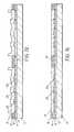
- FIG. 1is a perspective, partially cut-away view of a spatial light modulator with electromechanical conformal grating devices, showing two devices in a linear array;
- FIG. 2is a top view of a spatial light modulator with electromechanical conformal grating devices, showing four individually operable devices in a linear array;
- FIGS. 3 a and 3 bare cross-sectional views through line 3 , 7 , 9 , 10 — 3 , 7 , 9 , 10 in FIG. 2, showing the operation of an electromechanical conformal grating device in an unactuated state and an actuated state, respectively;
- FIGS. 4 a and 4 bare cross-sectional views through line 4 — 4 in FIG. 2 showing the device in an unactuated state and an actuated state, respectively;
- FIG. 5is a plot showing ribbon element position as a function of applied voltage
- FIG. 6is a diagram showing the device profile in response to two different actuation voltages
- FIG. 7 ais a cross-sectional view through line 3 , 7 , 9 , 10 — 3 , 7 , 9 , 10 in FIG. 2 illustrating the layer structure prior to any patterning;
- FIG. 7 bis a cross-sectional view through line 3 , 7 , 9 , 10 — 3 , 7 , 9 , 10 in FIG. 2 illustrating patterning of the active region to form channels and intermediate supports;
- FIG. 7 cis a cross-sectional view through line 3 , 7 , 9 , 10 — 3 , 7 , 9 , 10 in FIG. 2 illustrating deposition of a sacrificial layer;
- FIG. 7 dis a cross-sectional view through line 3 , 7 , 9 , 10 — 3 , 7 , 9 , 10 in FIG. 2 illustrating patterning of the sacrificial layer;
- FIG. 7 eis a cross-sectional view through line 3 , 7 , 9 , 10 — 3 , 7 , 9 , 10 in FIG. 2 illustrating planarizing of the sacrificial layer;
- FIG. 7 fis a cross-sectional view through line 3 , 7 , 9 , 10 — 3 , 7 , 9 , 10 in FIG. 2 illustrating deposition of a ribbon layer and a reflective and conductive layer;
- FIG. 7 gis a cross-sectional view through line 3 , 7 , 9 , 10 — 3 , 7 , 9 , 10 in FIG. 2 illustrating removal of the sacrificial layer after patterning elongated ribbon elements;
- FIG. 8is a top view of an alternate embodiment of the spatial light modulator
- FIG. 9 ais a cross sectional view of an alternative embodiment of the conformal grating device in an unactuated state.
- FIG. 9 bis a cross sectional view of an alternative embodiment of the conformal grating device in an actuated state.
- FIGS. 10 a - 10 fillustrate the fabrication steps used to make an alternative embodiment of the conformal grating device.
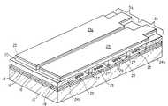
- FIG. 1shows the structure of two side-by-side conformal grating devices 5 a and 5 b in an unactuated state.
- the devicescan be operated by the application of an electrostatic force.
- a substrate 10 made of glass, metal, plastic, or semiconductor materialsis covered by a bottom conductive layer 12 .
- the grating devices 5 a and 5 bare formed on top of the bottom conductive layer 12 and the substrate 10 .
- the bottom conductive layer 12acts as an electrode to actuate the devices.
- the bottom conductive layer 12can be made of materials such as aluminum, titanium, gold, silver, tungsten, doped silicon, or indium tin oxide.
- a dielectric protective layer 14covers the bottom conductive layer 12 .
- a standoff layer 16is formed which is followed by a spacer layer 18 .
- a ribbon layer 20is formed which is covered by a reflective layer 22 .
- the reflective layer 22is also a conductor in order to provide electrodes for the actuation of the conformal grating devices 5 a and 5 b .
- the reflective and conductive layer 22is patterned to provide electrodes to the two conformal grating devices 5 a and 5 b .
- the ribbon layer 20preferably comprises a material with a sufficient tensile stress to provide a large restoring force.
- ribbon materialsare silicon nitride, titanium aluminide, and titanium oxide.
- the thickness and tensile stress of the ribbon layer 20are chosen to optimize performance by influencing the electrostatic force for actuation and the restoring force. These forces affect the voltage requirement, speed, and resonance frequency of the conformal grating devices 5 a and 5 b.
- Each of the two devices 5 a and 5 bhas an associated elongated ribbon element 23 a and 23 b , respectively, patterned from the reflective and conductive layer 22 and the ribbon layer 20 , and herein referred to as conductive reflective ribbon elements.
- the elongated-conductive reflective ribbon elements 23 a and 23 bare supported by end supports 24 a and 24 b formed from the spacer layer 18 and by one or more intermediate supports 27 . In FIG. 1, three intermediate supports 27 are shown formed from the spacer layer 18 . These intermediate supports 27 are uniformly separated in order to form four equal-width channels 25 .
- the conductive reflective ribbon elements 23 a and 23 bare secured to the end supports 24 a and 24 b and to the intermediate supports 27 .
- the end supports 24 a and 24 bare not defined other than at their edges facing the channel 25 .
- a plurality of square standoffs 29is patterned at the bottom of the channels 25 from the standoff layer 16 . These standoffs 29 reduce the possibility of the conductive reflective ribbon elements 23 a , 23 b sticking when actuated.
- the standoffs 29may also be patterned in shapes other than square, for example, rectangular or round.
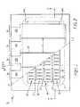
- FIG. 2A top view of a four-device linear array of conformal grating devices 5 a , 5 b , 5 c and 5 d is shown in FIG. 2 .
- the conductive reflective ribbon elements 23 a , 23 b , 23 c , and 23 dare depicted partially removed over the portion of the diagram below the line A—A in order to show the underlying structure.
- the intermediate supports 27must be completely hidden below the conductive reflective ribbon elements 23 a , 23 b , 23 c and 23 d . Therefore, when viewed from the top, the intermediate supports 27 must not be visible in the gaps 28 between the conformal grating devices 5 a - 5 d .
- each of the conformal grating deviceshas three intermediate supports 27 with four equal-width channels 25 .
- the active region 8is the portion of the device where the electromechanical actuation takes place and contains the channels 25 , the intermediate supports 27 , and the end supports 24 a and 24 b .
- the active region 8is completely covered by the ribbon layer 20 in the form of the elongated-conductive reflective ribbon elements 23 a , 23 b , 23 c , and 23 d.
- the center-to-center separation ⁇ of the intermediate supports 27defines the period of the conformal grating devices in the actuated state.
- the conductive reflective ribbon elements 23 a - 23 dare mechanically and electrically isolated from one another, allowing independent operation of the four conformal grating devices 5 a - 5 d.
- the bottom conductive layer 12 of FIG. 1can be common to all of the devices.
- FIG. 3 ais a side view, through line 3 , 7 , 9 , 10 — 3 , 7 , 9 , 10 of FIG. 2, of two channels 25 of the conformal grating device 5 b in the unactuated state.
- FIG. 3 bshows the same view of the actuated state.
- an attractive electrostatic forceis produced by applying a voltage difference between the bottom conductive layer 12 and the reflective and conductive layer 22 of the conductive reflective ribbon element 23 b .
- the ribbon element 23 bis suspended flat between the end supports 24 a , 24 b .
- an incident light beam 30is primarily reflected 32 into the mirror direction.
- FIG. 3 bshows the device in the fully actuated state with the conductive reflective ribbon element 23 b in contact with the standoffs 29 .
- the height difference between the bottom of element 23 b and the top of the standoffs 29is chosen to be approximately 1 ⁇ 4 of the wavelength ⁇ of the incident light. The optimum height depends on the specific shape of the actuated device.
- the incident light beam 30is primarily diffracted into the +1st order 35 a and ⁇ 1st order 35 b , with additional light diffracted into the +2nd order 36 a and ⁇ 2nd order 36 b .
- a small amount of lightis diffracted into even higher orders and some is reflected.
- the angle ⁇ m between the incident beam and the mth order diffracted beamis given by
- One or more of the diffracted orderscan be collected and used by the optical system, depending on the application.
- the applied voltageis removed, the forces due to the tensile stress and bending restores the ribbon element 23 b to its original unactuated state.
- FIGS. 4 a and 4 bshow a rotated side view through line 4 — 4 of FIG. 2 of the conformal grating device 5 b in the unactuated and actuated states, respectively.
- the conductive reflective ribbon element 23 bis suspended by the end support 24 b and the adjacent intermediate support 27 (not shown in this perspective).
- the application of a voltageactuates the device as illustrated in FIG. 4 b.
- Substrate materialsilicon
- Bottom conductive layerdoped silicon
- Width of conductive reflective ribbon element w30 ⁇ m
- the resonant frequency of the ribbon elements in this particular designis approximately 11 MHz. Most practical designs have resonant frequencies between 2 MHz and 15 MHz. Because of this high resonance, the switching time of the device can be very short.
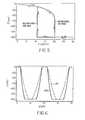
- FIGS. 5 and 6show the modeled electromechanical operation of this particular device.
- FIG. 5is a plot of the position of the conductive reflective ribbon element at the center of a channel as a function of applied voltage, illustrating the associated hysteresis.
- the center displacementincreases in approximately a quadratic manner until the pull-down voltage of 20.1 V is reached.
- the electrostatic forceovercomes the tensile restoring force and the ribbon slams into the substrate.
- Further increasing the applied voltagechanges the shape of the deformed ribbon, but cannot change the center position.
- the voltageWith the ribbon in contact with the substrate, the voltage can be reduced below the pull-down value while maintaining contact, until release at 10.8 V.
- This hysteresiscan be exploited to improve the optical performance of the device. It can also be used as a switch in certain applications.
- FIG. 6demonstrates how the grating profile may be modified by adjusting the applied voltage.
- the profile of two periods of the actuated deviceis shown at 12 V (dotted line) and at 22 V (solid line), with the ribbon and substrate in contact.
- 12 V profilecontact must first be established by applying a value larger than the pull-down voltage of 20.1 V. Because 12 V is only slightly larger that the release voltage, only a small portion of the ribbon touches the substrate. This change in shape with voltage has an important impact on the diffraction efficiency of the device.
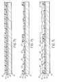
- FIGS. 7 a - 7 gThe fabrication sequence for making a conformal grating device is illustrated in FIGS. 7 a - 7 g .
- FIG. 7 awhich is a cross-sectional view along line 3 , 7 , 9 , 10 — 3 , 7 , 9 , 10 indicated in FIG. 2, illustrated is the built-up layer of one embodiment of the invention with standoffs 29 formed at the bottom of the channels 25 .
- the deviceis built upon a substrate 10 , covered by the bottom conductive layer 12 , and a dielectric protective layer 14 on top of the bottom conductive layer 12 .
- the substrate 10can be glass, plastic, metal, or a semiconductor material.
- the substrate 10is silicon and the dielectric protective layer 14 is a thermal oxide.
- a standoff layer 16is deposited followed by a spacer layer 18 .
- the spacer layer 18is selected from the group consisting of silicon oxide, silicon nitride polysilicon, and polyimide.
- the standoff layer 16is silicon nitride deposited by chemical vapor deposition.
- the top surface of the standoff layer 16will be used to define an actuation height resulting from operation.
- the spacer layer 18is silicon oxide deposited by chemical vapor deposition.
- the total height of the actuation of the elongated-conductive reflective ribbon elements 23 a - 23 dis defined by the thickness of the spacer layer 18 .
- FIG. 7 bis a cross-sectional view along line 3 , 7 , 9 , 10 — 3 , 7 , 9 , 10 indicated in FIG. 2, etching of the channels 25 to form the intermediate supports 27 is illustrated.
- the patterning of the spacer layer 18is carried out using standard photolithographic processing and etching methods to define the active region 8 where the channels 25 and intermediate supports 27 are located.
- the etching of the oxide spacer layeruses chemistry designed to stop on the silicon nitride standoff layer 16 .
- the standoff layer 16is then patterned using photolithographic processing and etching methods to produce the standoffs 29 , as illustrated in FIG. 7 b .
- the standoffs 29act as mechanical stops for the actuation of the conformal grating device.
- the actuated elongated-conductive reflective ribbon elements 23 a - 23 dcome into contact with the surface standoffs 29 .
- FIG. 7 cis a cross-sectional view along line 3 , 7 , 9 , 10 — 3 , 7 , 9 , 10 indicated in FIG. 2, the deposition of a sacrificial layer 19 is illustrated.
- a conformal sacrificial layer 19is deposited to a thickness greater than the sum of the thickness of the standoff layer 16 and the spacer layer 18 .
- the material for the sacrificial layer 19is different from the spacer layer 18 and is selected from the group consisting of silicon oxide, silicon nitride, polysilicon, doped-polysilicon, silicon-germanium alloys, and polyimide.
- the sacrificial layer 19is polysilicon deposited by chemical vapor deposition.
- FIG. 7 dis a cross-sectional view along line 3 , 7 , 9 , 10 — 3 , 7 , 9 , 10 indicated in FIG. 2, the patterning of the sacrificial layer 19 is illustrated.
- the patterning of the sacrificial layer 19is carried out using standard photolithographic processing and a mask which is the reverse of the mask used to etch the spacer layer 18 defining the active region 8 where the channels 25 and intermediate supports 27 are located.
- the maskcan be biased to account for misalignment.
- the sacrificial layer 19is then completely removed from the intermediate supports 27 and the areas outside of the active region 8 .
- the removal of the sacrificial layer 19 outside of the active region 8improves the uniformity of the planarization step described below.
- the removal of the sacrificial layer 19may be done prior to providing the ribbon layer 20 . This removal process ensures good mechanical attachment of the elongated-conductive reflective ribbon elements 23 a - 23 d to the intermediate supports 27 and the end supports 24 a and 25 b (not shown in FIG. 7 d ).
- FIG. 7 eis a cross-sectional view along line 3 , 7 , 9 , 10 — 3 , 7 , 9 , 10 indicated in FIG. 2, the planarization of the sacrificial layer 19 to a level substantially near the top surface of the intermediate supports 27 is illustrated.
- Chemical mechanical polishing methodsare used to achieve the polished structure.
- the polished surface of sacrificial layer 19 filling the channels 25is preferably polished to be optically coplanar with the top surface of the intermediate supports 27 . As is well known in the practice of optical engineering, this requires a surface planarity of less than about 200 Angstrom units at visible wavelengths.
- FIG. 7 fis a cross-sectional view along line 3 , 7 , 9 , 10 — 3 , 7 , 9 , 10 indicated in FIG. 2, deposition of the ribbon layer 20 and of the reflective and conductive layer 22 to illustrate.
- the ribbon layer 20is provided on top of the optically-coplanar sacrificial layer 19 and intermediate supports 27 , thereby also covering the entire active region 8 of the device.
- Silicon nitrideis a well-suited material for the ribbon layer 20 and can be patterned to provide the needed mechanical structure. Its material properties are well suited for the application because of the intrinsic tensile stress easily controlled by the deposition process.
- titanium aluminideis used as the ribbon layer 20 material.
- Titanium aluminideis also electrically conducting.
- the reflective and conductive layer 22 deposited atop the ribbon layer 20needs to have good electric conducting properties.
- the light reflecting properties of the reflective and conductive layer 22improve the efficiency of diffraction so as to maximize the diffracted light and minimize loss of light by absorption.
- the material for the reflective and conductive layer 22is selected from the group consisting of aluminum, titanium, gold, silver, tungsten, silicon alloys, and indium tin oxide.
- Electrical contact to the bottom conductive layercan be made from the back side through the substrate 10 if the substrate is electrically conductive. Alternatively electrical contact can be made on the front side by photolithographically patterning areas outside the active region (not shown) and etching through the spacer layer 18 , standoff layer 16 and dielectric protective layer 14 .
- the elongated-conductive reflective ribbon elements 23 a - 23 dare now patterned from the ribbon layer 20 and the reflective and conductive layer 22 using photolithographic processing and etching. This etching process defines the top-view geometry of the elongated-conductive reflective ribbon elements 23 a - 23 d shown in FIGS. 1 and 2.
- FIG. 7 gis a cross-sectional view along line 3 , 7 , 9 , 10 — 3 , 7 , 9 , 10 indicated in FIG. 2, the removal of the sacrificial layer 19 from within the active region 8 to form channels 25 and intermediate supports 27 is illustrated.
- the sacrificial layer 19is polysilicon which can be selectively removed by dry etching methods using xenon difluoride to yield the cross-sectional view illustrated in FIG. 7 g .
- the gashas access to the sacrificial layer 19 through the gaps 28 between the elongated-conductive reflective ribbon elements 23 a - 23 d .
- the removal of the sacrificial layer 19is the final step needed to produce operational conformal grating devices 5 a - 5 d .
- the devicescan now be actuated to operate as described earlier.
- the elongated-conductive reflective ribbon elements 23 a - 23 dremain optically coplanar providing the ribbon layer 20 is deposited with uniform thickness and uniform tensile stress.
- FIG. 8An alternate embodiment of conformal grating devices is shown in FIG. 8, which depicts a top view of a four-device linear array similar to FIG. 2 .
- Each of the conformal grating devices 5 a , 5 b , 5 c and 5 dnow has an associated pair of subdivided elongated-conductive reflective ribbon elements ( 51 a, 52 a ), ( 51 b , 52 b ), ( 51 c, 52 c ) and ( 51 d, 52 d ), respectively.
- This subdivision of each devicepermits fabrication of wider devices without significantly impacting optical performance.
- the preferred method of fabricationis to etch a sacrificial layer from the channel, thus releasing the ribbon elements.
- the subdivided gaps 55 between the elementsallow the etchant to access this sacrificial layer. Increasing the number of subdivided gaps 55 can therefore improve the etching process.
- the conductive reflective ribbon elementsare depicted partially removed over the portion of the diagram below the line A—A in order to show the underlying structure.
- the intermediate supports 27must be completely hidden below the conductive reflective ribbon elements 51 a , 52 a , 51 b , 52 b , 51 c , 52 c , 51 d and 52 d . Therefore, when viewed from the top, the intermediate supports 27 must not penetrate into the subdivided gaps 55 .
- the ribbon elements within a single conformal grating deviceare mechanically isolated, but electrically coupled. They therefore operate in unison when a voltage is applied.
- FIGS. 9 a and 9 bshow an alternate embodiment that reduces this problem.
- the side viewis the same as in FIGS. 3 a and 3 b .
- FIG. 9 adepicts the two channels 25 between the three intermediate supports 27 of the device in the unactuated state.
- FIG. 9 bshows the same view of the actuated state.
- the ribbon element 23 bIn the unactuated state, with no voltage applied to the device, the ribbon element 23 b is suspended flat above the intermediate supports 27 by the two end supports 24 a and 24 b (see FIG. 2 ), leaving a small intermediate support gap 60 between the top of the intermediate supports 27 and the bottom of the ribbon element 23 b .
- the bottom of the ribbon element 23 bmakes contact with the top of the intermediate supports and a partially conforming grating is created.
- FIG. 9 bshows the device in the fully actuated state with the conductive reflective ribbon element 23 b also touching the standoffs 29 .
- FIGS. 10 a - 10 fillustrate the fabrication sequence for making the conformal grating device with elongated-conductive reflective ribbon elements suspended above intermediate supports. These figures show the same view of the device as FIGS. 9 a and 9 b . The first few steps are the same as the process of FIGS. 7 a and 7 b .
- the deviceis built upon a substrate 10 , covered by the bottom conductive layer 12 , and a dielectric protective layer 14 on top of the bottom conductive layer 12 .
- a standoff layer 16is deposited followed by a spacer layer 18 .
- FIG. 10 billustrates etching of the channels 25 to form the intermediate supports 27 .
- the patterning of the spacer layer 18is carried out using standard photolithographic processing and etching methods to define the active region 8 where the channels 25 and intermediate supports 27 are located.
- the standoff layer 16is then patterned using photolithographic processing and etching methods to produce the standoffs 29 , as illustrated in FIG. 10 b.
- the end supports 24 a and 24 bcan be fabricated to be higher than the intermediate supports 27 (not shown in FIG. 10 b ).
- This stepcan be performed by depositing and patterning a support layer made, for example, of silicon nitride to increase the height of the end supports 24 a and 24 b relative to the intermediate supports.
- FIG. 10 cillustrates deposition of a conformal sacrificial layer 19 on top of the structure from FIG. 10 b.
- the thickness of the sacrificial layermust be substantially greater that the sum of the thickness of the standoff layer 16 and the thickness of the spacer layer 18 .
- FIG. 10 dillustrates planarization of the sacrificial layer 19 to a level above the top surface of the intermediate supports 27 .
- the sacrificial layer 19needs to be substantially flat after planarization with some sacrificial material left above the intermediate supports 27 to prevent attachment of the elongated-conductive reflective ribbon element 23 b to the intermediate supports 27 .
- FIG. 10 fillustrates removal of the sacrificial layer 19 from within the active region 8 to reveal channels 25 and intermediate supports 27 .
- This stepalso removes the sacrificial layer 19 from the intermediate support gap 60 , thereby suspending the elongated-conductive reflective ribbon element 27 above the top surface of the intermediate supports 27 .
- the elongated-conductive reflective ribbon element 23 bis held in tension above the intermediate supports 27 by the two end supports 24 a and 24 b (not shown in FIG. 10 f ).
- the removal of the sacrificial layer 19is the final step needed to produce operational devices.
Landscapes
- Physics & Mathematics (AREA)
- General Physics & Mathematics (AREA)
- Optics & Photonics (AREA)
- Mechanical Light Control Or Optical Switches (AREA)
- Diffracting Gratings Or Hologram Optical Elements (AREA)
- Micromachines (AREA)
Abstract
Description
Claims (29)
Priority Applications (2)
| Application Number | Priority Date | Filing Date | Title |
|---|---|---|---|
| US09/867,927US6663788B2 (en) | 2000-01-26 | 2001-05-30 | Method for manufacturing a mechanical conformal grating device |
| US10/158,516US6663790B2 (en) | 2000-01-26 | 2002-05-30 | Method for manufacturing a mechanical conformal grating device with improved contrast and lifetime |
Applications Claiming Priority (2)
| Application Number | Priority Date | Filing Date | Title |
|---|---|---|---|
| US09/491,354US6307663B1 (en) | 2000-01-26 | 2000-01-26 | Spatial light modulator with conformal grating device |
| US09/867,927US6663788B2 (en) | 2000-01-26 | 2001-05-30 | Method for manufacturing a mechanical conformal grating device |
Related Parent Applications (1)
| Application Number | Title | Priority Date | Filing Date |
|---|---|---|---|
| US09/491,354Continuation-In-PartUS6307663B1 (en) | 2000-01-26 | 2000-01-26 | Spatial light modulator with conformal grating device |
Related Child Applications (1)
| Application Number | Title | Priority Date | Filing Date |
|---|---|---|---|
| US10/158,516Continuation-In-PartUS6663790B2 (en) | 2000-01-26 | 2002-05-30 | Method for manufacturing a mechanical conformal grating device with improved contrast and lifetime |
Publications (2)
| Publication Number | Publication Date |
|---|---|
| US20010024325A1 US20010024325A1 (en) | 2001-09-27 |
| US6663788B2true US6663788B2 (en) | 2003-12-16 |
Family
ID=23951835
Family Applications (2)
| Application Number | Title | Priority Date | Filing Date |
|---|---|---|---|
| US09/491,354Expired - Fee RelatedUS6307663B1 (en) | 2000-01-26 | 2000-01-26 | Spatial light modulator with conformal grating device |
| US09/867,927Expired - Fee RelatedUS6663788B2 (en) | 2000-01-26 | 2001-05-30 | Method for manufacturing a mechanical conformal grating device |
Family Applications Before (1)
| Application Number | Title | Priority Date | Filing Date |
|---|---|---|---|
| US09/491,354Expired - Fee RelatedUS6307663B1 (en) | 2000-01-26 | 2000-01-26 | Spatial light modulator with conformal grating device |
Country Status (4)
| Country | Link |
|---|---|
| US (2) | US6307663B1 (en) |
| EP (1) | EP1122577B1 (en) |
| JP (1) | JP2001215317A (en) |
| DE (1) | DE60121838T2 (en) |
Cited By (11)
| Publication number | Priority date | Publication date | Assignee | Title |
|---|---|---|---|---|
| US20030215968A1 (en)* | 2002-05-15 | 2003-11-20 | Peterson Jeffrey J. | Fabrication of optical components using Si, SiGe, SiGeC, and chemical endpoint detection |
| US20040076008A1 (en)* | 2001-12-26 | 2004-04-22 | Koichi Ikeda | Electrostatic drive type mems element, manufacturing method thereof, optical mems element, optical modulation element, glv device, and laser display |
| US20040201891A1 (en)* | 2001-05-03 | 2004-10-14 | Martti Schrader | Electrically reconfigurable optical devices |
| US20080180020A1 (en)* | 2007-01-29 | 2008-07-31 | Cok Ronald S | Light-emitting display device having improved efficiency |
| US20090147220A1 (en)* | 2007-12-05 | 2009-06-11 | Agostinelli John A | Display apparatus using bilinear electromechanical modulator |
| US20090231697A1 (en)* | 2008-03-13 | 2009-09-17 | Marcus Michael A | Stereoscopic display using multi-linear electromechanical modulator |
| US20090278918A1 (en)* | 2008-05-07 | 2009-11-12 | Marcus Michael A | Display using bidirectionally scanned linear modulator |
| US20100171931A1 (en)* | 2009-01-07 | 2010-07-08 | David Kessler | Line illumination apparatus using laser arrays |
| US20100315595A1 (en)* | 2009-06-15 | 2010-12-16 | Marcus Michael A | Dynamic illumination control for laser projection display |
| US20110134344A1 (en)* | 2009-12-08 | 2011-06-09 | Marcus Michael A | Dynamic illumination control for laser projection display |
| US8233035B2 (en) | 2009-01-09 | 2012-07-31 | Eastman Kodak Company | Dual-view stereoscopic display using linear modulator arrays |
Families Citing this family (139)
| Publication number | Priority date | Publication date | Assignee | Title |
|---|---|---|---|---|
| US6724125B2 (en) | 1999-03-30 | 2004-04-20 | Massachusetts Institute Of Technology | Methods and apparatus for diffractive optical processing using an actuatable structure |
| US6960305B2 (en)* | 1999-10-26 | 2005-11-01 | Reflectivity, Inc | Methods for forming and releasing microelectromechanical structures |
| US6639713B2 (en) | 2000-04-25 | 2003-10-28 | Umachines, Inc. | Silicon micromachined optical device |
| US6709886B2 (en) | 2000-04-25 | 2004-03-23 | Umachines, Inc. | Method of fabricating micromachined devices |
| US6411425B1 (en)* | 2000-09-27 | 2002-06-25 | Eastman Kodak Company | Electromechanical grating display system with spatially separated light beams |
| JP2002162599A (en)* | 2000-11-24 | 2002-06-07 | Sony Corp | Stereoscopic image display device |
| US6384959B1 (en)* | 2001-01-09 | 2002-05-07 | Eastman Kodak Company | Optical data modulation system with self-damped electromechanical conformal grating |
| US6661561B2 (en)* | 2001-03-26 | 2003-12-09 | Creo Inc. | High frequency deformable mirror device |
| US6856448B2 (en)* | 2001-03-26 | 2005-02-15 | Creo Inc. | Spatial light modulator |
| US6594060B2 (en)* | 2001-03-29 | 2003-07-15 | Eastman Kodak Company | Electromechanical conformal grating device with improved optical efficiency and contrast |
| US6621615B2 (en) | 2001-07-25 | 2003-09-16 | Eastman Kodak Company | Method and system for image display |
| US6587253B2 (en)* | 2001-08-16 | 2003-07-01 | Silicon Light Machines | Enhance thermal stability through optical segmentation |
| US6594090B2 (en) | 2001-08-27 | 2003-07-15 | Eastman Kodak Company | Laser projection display system |
| US7046410B2 (en) | 2001-10-11 | 2006-05-16 | Polychromix, Inc. | Actuatable diffractive optical processor |
| US6611380B2 (en) | 2001-12-21 | 2003-08-26 | Eastman Kodak Company | System and method for calibration of display system with linear array modulator |
| US6577429B1 (en) | 2002-01-15 | 2003-06-10 | Eastman Kodak Company | Laser projection display system |
| KR100908510B1 (en)* | 2002-02-26 | 2009-07-20 | 유니-픽셀 디스플레이스, 인코포레이티드 | Air gap spontaneous mechanism |
| US6590695B1 (en) | 2002-02-26 | 2003-07-08 | Eastman Kodak Company | Micro-mechanical polarization-based modulator |
| WO2003079384A2 (en)* | 2002-03-11 | 2003-09-25 | Uni-Pixel Displays, Inc. | Double-electret mems actuator |
| US6768585B2 (en) | 2002-05-02 | 2004-07-27 | Eastman Kodak Company | Monocentric autostereoscopic optical apparatus using a scanned linear electromechanical modulator |
| WO2003094138A2 (en)* | 2002-05-06 | 2003-11-13 | Uni-Pixel Displays, Inc. | Field sequential color efficiency |
| US6678085B2 (en) | 2002-06-12 | 2004-01-13 | Eastman Kodak Company | High-contrast display system with scanned conformal grating device |
| US6908201B2 (en)* | 2002-06-28 | 2005-06-21 | Silicon Light Machines Corporation | Micro-support structures |
| US6779892B2 (en)* | 2002-07-26 | 2004-08-24 | Eastman Kodak Company | Monocentric autostereoscopic optical display having an expanded color gamut |
| US6844960B2 (en)* | 2002-09-24 | 2005-01-18 | Eastman Kodak Company | Microelectromechanical device with continuously variable displacement |
| US6967986B2 (en)* | 2002-10-16 | 2005-11-22 | Eastman Kodak Company | Light modulation apparatus using a VCSEL array with an electromechanical grating device |
| US6802613B2 (en) | 2002-10-16 | 2004-10-12 | Eastman Kodak Company | Broad gamut color display apparatus using an electromechanical grating device |
| US6747785B2 (en)* | 2002-10-24 | 2004-06-08 | Hewlett-Packard Development Company, L.P. | MEMS-actuated color light modulator and methods |
| US6807010B2 (en)* | 2002-11-13 | 2004-10-19 | Eastman Kodak Company | Projection display apparatus having both incoherent and laser light sources |
| US6947459B2 (en)* | 2002-11-25 | 2005-09-20 | Eastman Kodak Company | Organic vertical cavity laser and imaging system |
| US6717714B1 (en)* | 2002-12-16 | 2004-04-06 | Eastman Kodak Company | Method and system for generating enhanced gray levels in an electromechanical grating display |
| US7057819B1 (en)* | 2002-12-17 | 2006-06-06 | Silicon Light Machines Corporation | High contrast tilting ribbon blazed grating |
| US6724515B1 (en)* | 2002-12-31 | 2004-04-20 | Eastman Kodak Company | Conformal grating device for producing enhanced gray levels |
| JP2004219843A (en)* | 2003-01-16 | 2004-08-05 | Seiko Epson Corp | Optical modulator, display device and manufacturing method thereof |
| US6863382B2 (en)* | 2003-02-06 | 2005-03-08 | Eastman Kodak Company | Liquid emission device having membrane with individually deformable portions, and methods of operating and manufacturing same |
| US6930817B2 (en)* | 2003-04-25 | 2005-08-16 | Palo Alto Research Center Incorporated | Configurable grating based on surface relief pattern for use as a variable optical attenuator |
| CN1297830C (en)* | 2003-06-05 | 2007-01-31 | 华新丽华股份有限公司 | Producing method for raster structure |
| US7111943B2 (en)* | 2003-07-28 | 2006-09-26 | Eastman Kodak Company | Wide field display using a scanned linear light modulator array |
| US6886940B2 (en)* | 2003-08-28 | 2005-05-03 | Eastman Kodak Company | Autostereoscopic display for multiple viewers |
| US20050073471A1 (en)* | 2003-10-03 | 2005-04-07 | Uni-Pixel Displays, Inc. | Z-axis redundant display/multilayer display |
| US7148910B2 (en)* | 2003-11-06 | 2006-12-12 | Eastman Kodak Company | High-speed pulse width modulation system and method for linear array spatial light modulators |
| CN1902673B (en)* | 2003-11-14 | 2011-06-15 | 单方图素显示股份有限公司 | Matrix addressing device and display and system comprising same |
| US6984039B2 (en)* | 2003-12-01 | 2006-01-10 | Eastman Kodak Company | Laser projector having silhouette blanking for objects in the output light path |
| US7274500B2 (en)* | 2003-12-03 | 2007-09-25 | Eastman Kodak Company | Display system incorporating trilinear electromechanical grating device |
| US7476327B2 (en) | 2004-05-04 | 2009-01-13 | Idc, Llc | Method of manufacture for microelectromechanical devices |
| US7289209B2 (en)* | 2004-07-22 | 2007-10-30 | Eastman Kodak Company | Programmable spectral imaging system |
| US7564874B2 (en)* | 2004-09-17 | 2009-07-21 | Uni-Pixel Displays, Inc. | Enhanced bandwidth data encoding method |
| US7583429B2 (en) | 2004-09-27 | 2009-09-01 | Idc, Llc | Ornamental display device |
| US7936497B2 (en) | 2004-09-27 | 2011-05-03 | Qualcomm Mems Technologies, Inc. | MEMS device having deformable membrane characterized by mechanical persistence |
| US7304784B2 (en) | 2004-09-27 | 2007-12-04 | Idc, Llc | Reflective display device having viewable display on both sides |
| US7630119B2 (en) | 2004-09-27 | 2009-12-08 | Qualcomm Mems Technologies, Inc. | Apparatus and method for reducing slippage between structures in an interferometric modulator |
| US7130104B2 (en) | 2004-09-27 | 2006-10-31 | Idc, Llc | Methods and devices for inhibiting tilting of a mirror in an interferometric modulator |
| US7564612B2 (en) | 2004-09-27 | 2009-07-21 | Idc, Llc | Photonic MEMS and structures |
| US7527995B2 (en)* | 2004-09-27 | 2009-05-05 | Qualcomm Mems Technologies, Inc. | Method of making prestructure for MEMS systems |
| US7372613B2 (en) | 2004-09-27 | 2008-05-13 | Idc, Llc | Method and device for multistate interferometric light modulation |
| US7420725B2 (en) | 2004-09-27 | 2008-09-02 | Idc, Llc | Device having a conductive light absorbing mask and method for fabricating same |
| US7944599B2 (en) | 2004-09-27 | 2011-05-17 | Qualcomm Mems Technologies, Inc. | Electromechanical device with optical function separated from mechanical and electrical function |
| US7612932B2 (en) | 2004-09-27 | 2009-11-03 | Idc, Llc | Microelectromechanical device with optical function separated from mechanical and electrical function |
| US7302157B2 (en) | 2004-09-27 | 2007-11-27 | Idc, Llc | System and method for multi-level brightness in interferometric modulation |
| US8008736B2 (en) | 2004-09-27 | 2011-08-30 | Qualcomm Mems Technologies, Inc. | Analog interferometric modulator device |
| US7554714B2 (en) | 2004-09-27 | 2009-06-30 | Idc, Llc | Device and method for manipulation of thermal response in a modulator |
| US7289259B2 (en) | 2004-09-27 | 2007-10-30 | Idc, Llc | Conductive bus structure for interferometric modulator array |
| US20060077545A1 (en)* | 2004-10-08 | 2006-04-13 | Eastman Kodak Company | Apparatus to align stereoscopic display |
| US7046446B1 (en) | 2004-12-15 | 2006-05-16 | Eastman Kodak Company | Speckle reduction for display system with electromechanical grating |
| US7119936B2 (en)* | 2004-12-15 | 2006-10-10 | Eastman Kodak Company | Speckle reduction for display system with electromechanical grating |
| US7054054B1 (en) | 2004-12-20 | 2006-05-30 | Palo Alto Research Center Incorporated | Optical modulator with a traveling surface relief pattern |
| US7249853B2 (en)* | 2005-04-13 | 2007-07-31 | Eastman Kodak Company | Unpolished optical element with periodic surface roughness |
| KR100832622B1 (en)* | 2005-05-25 | 2008-05-27 | 삼성전기주식회사 | Optical modulator and mobile unit using the projector of optical modulator |
| US7884989B2 (en) | 2005-05-27 | 2011-02-08 | Qualcomm Mems Technologies, Inc. | White interferometric modulators and methods for forming the same |
| KR100897666B1 (en)* | 2005-07-20 | 2009-05-14 | 삼성전기주식회사 | Display apparatus which scans both the forward path and backward path |
| EP1754683A1 (en)* | 2005-08-18 | 2007-02-21 | Fraunhofer-Gesellschaft zur Förderung der angewandten Forschung e.V. | Micromechanical element |
| US7411722B2 (en)* | 2005-08-24 | 2008-08-12 | Eastman Kodak Company | Display system incorporating bilinear electromechanical grating device |
| US7408558B2 (en)* | 2005-08-25 | 2008-08-05 | Eastman Kodak Company | Laser-based display having expanded image color |
| US7449759B2 (en)* | 2005-08-30 | 2008-11-11 | Uni-Pixel Displays, Inc. | Electromechanical dynamic force profile articulating mechanism |
| US8509582B2 (en)* | 2005-08-30 | 2013-08-13 | Rambus Delaware Llc | Reducing light leakage and improving contrast ratio performance in FTIR display devices |
| KR100832621B1 (en)* | 2005-09-23 | 2008-05-27 | 삼성전기주식회사 | Mobile projector with forward and backward scanning |
| US7274454B2 (en)* | 2005-12-23 | 2007-09-25 | Eastman Kodak Company | Imaging system with programmable spectral switch |
| US7342658B2 (en)* | 2005-12-28 | 2008-03-11 | Eastman Kodak Company | Programmable spectral imaging system |
| US7916980B2 (en) | 2006-01-13 | 2011-03-29 | Qualcomm Mems Technologies, Inc. | Interconnect structure for MEMS device |
| WO2007089770A2 (en) | 2006-01-31 | 2007-08-09 | Polychromix Corporation | Hand-held ir spectrometer with a fixed grating and a diffractive mems-array |
| US7649671B2 (en) | 2006-06-01 | 2010-01-19 | Qualcomm Mems Technologies, Inc. | Analog interferometric modulator device with electrostatic actuation and release |
| US7980671B2 (en)* | 2006-06-06 | 2011-07-19 | Xerox Corporation | Electrostatic actuator and method of making the electrostatic actuator |
| US7835061B2 (en) | 2006-06-28 | 2010-11-16 | Qualcomm Mems Technologies, Inc. | Support structures for free-standing electromechanical devices |
| US7527998B2 (en) | 2006-06-30 | 2009-05-05 | Qualcomm Mems Technologies, Inc. | Method of manufacturing MEMS devices providing air gap control |
| KR100905554B1 (en)* | 2006-08-30 | 2009-07-02 | 삼성전기주식회사 | Portable terminal with projector using optical modulator |
| US7629197B2 (en) | 2006-10-18 | 2009-12-08 | Qualcomm Mems Technologies, Inc. | Spatial light modulator |
| EP2104930A2 (en) | 2006-12-12 | 2009-09-30 | Evans & Sutherland Computer Corporation | System and method for aligning rgb light in a single modulator projector |
| US8115987B2 (en) | 2007-02-01 | 2012-02-14 | Qualcomm Mems Technologies, Inc. | Modulating the intensity of light from an interferometric reflector |
| US7742220B2 (en) | 2007-03-28 | 2010-06-22 | Qualcomm Mems Technologies, Inc. | Microelectromechanical device and method utilizing conducting layers separated by stops |
| US7643202B2 (en) | 2007-05-09 | 2010-01-05 | Qualcomm Mems Technologies, Inc. | Microelectromechanical system having a dielectric movable membrane and a mirror |
| US7715085B2 (en) | 2007-05-09 | 2010-05-11 | Qualcomm Mems Technologies, Inc. | Electromechanical system having a dielectric movable membrane and a mirror |
| US7719752B2 (en)* | 2007-05-11 | 2010-05-18 | Qualcomm Mems Technologies, Inc. | MEMS structures, methods of fabricating MEMS components on separate substrates and assembly of same |
| US7643199B2 (en) | 2007-06-19 | 2010-01-05 | Qualcomm Mems Technologies, Inc. | High aperture-ratio top-reflective AM-iMod displays |
| US7782517B2 (en) | 2007-06-21 | 2010-08-24 | Qualcomm Mems Technologies, Inc. | Infrared and dual mode displays |
| US7630121B2 (en) | 2007-07-02 | 2009-12-08 | Qualcomm Mems Technologies, Inc. | Electromechanical device with optical function separated from mechanical and electrical function |
| EP2183623A1 (en) | 2007-07-31 | 2010-05-12 | Qualcomm Mems Technologies, Inc. | Devices for enhancing colour shift of interferometric modulators |
| US7847999B2 (en) | 2007-09-14 | 2010-12-07 | Qualcomm Mems Technologies, Inc. | Interferometric modulator display devices |
| US7773286B2 (en)* | 2007-09-14 | 2010-08-10 | Qualcomm Mems Technologies, Inc. | Periodic dimple array |
| CN101828145B (en) | 2007-10-19 | 2012-03-21 | 高通Mems科技公司 | Displays with integrated photovoltaic elements |
| US8058549B2 (en) | 2007-10-19 | 2011-11-15 | Qualcomm Mems Technologies, Inc. | Photovoltaic devices with integrated color interferometric film stacks |
| EP2203765A1 (en) | 2007-10-23 | 2010-07-07 | Qualcomm Mems Technologies, Inc. | Adjustably transmissive mems-based devices |
| US8941631B2 (en) | 2007-11-16 | 2015-01-27 | Qualcomm Mems Technologies, Inc. | Simultaneous light collection and illumination on an active display |
| US7715079B2 (en) | 2007-12-07 | 2010-05-11 | Qualcomm Mems Technologies, Inc. | MEMS devices requiring no mechanical support |
| US8164821B2 (en) | 2008-02-22 | 2012-04-24 | Qualcomm Mems Technologies, Inc. | Microelectromechanical device with thermal expansion balancing layer or stiffening layer |
| US7944604B2 (en) | 2008-03-07 | 2011-05-17 | Qualcomm Mems Technologies, Inc. | Interferometric modulator in transmission mode |
| US7612933B2 (en) | 2008-03-27 | 2009-11-03 | Qualcomm Mems Technologies, Inc. | Microelectromechanical device with spacing layer |
| US7898723B2 (en) | 2008-04-02 | 2011-03-01 | Qualcomm Mems Technologies, Inc. | Microelectromechanical systems display element with photovoltaic structure |
| US7969638B2 (en) | 2008-04-10 | 2011-06-28 | Qualcomm Mems Technologies, Inc. | Device having thin black mask and method of fabricating the same |
| US8358317B2 (en) | 2008-05-23 | 2013-01-22 | Evans & Sutherland Computer Corporation | System and method for displaying a planar image on a curved surface |
| US8702248B1 (en) | 2008-06-11 | 2014-04-22 | Evans & Sutherland Computer Corporation | Projection method for reducing interpixel gaps on a viewing surface |
| US8023167B2 (en) | 2008-06-25 | 2011-09-20 | Qualcomm Mems Technologies, Inc. | Backlight displays |
| US7768690B2 (en) | 2008-06-25 | 2010-08-03 | Qualcomm Mems Technologies, Inc. | Backlight displays |
| US7746539B2 (en) | 2008-06-25 | 2010-06-29 | Qualcomm Mems Technologies, Inc. | Method for packing a display device and the device obtained thereof |
| US7859740B2 (en) | 2008-07-11 | 2010-12-28 | Qualcomm Mems Technologies, Inc. | Stiction mitigation with integrated mech micro-cantilevers through vertical stress gradient control |
| US7855826B2 (en) | 2008-08-12 | 2010-12-21 | Qualcomm Mems Technologies, Inc. | Method and apparatus to reduce or eliminate stiction and image retention in interferometric modulator devices |
| US8358266B2 (en) | 2008-09-02 | 2013-01-22 | Qualcomm Mems Technologies, Inc. | Light turning device with prismatic light turning features |
| US20100066770A1 (en)* | 2008-09-18 | 2010-03-18 | Eastman Kodak Company | Pulse Width Modulation Display Pixels with Spatial Manipulation |
| US8077378B1 (en) | 2008-11-12 | 2011-12-13 | Evans & Sutherland Computer Corporation | Calibration system and method for light modulation device |
| US20100177129A1 (en)* | 2009-01-12 | 2010-07-15 | Fredlund John R | Artifact reduction in optical scanning displays |
| US20100176855A1 (en)* | 2009-01-12 | 2010-07-15 | Huffman James D | Pulse width modulated circuitry for integrated devices |
| US20100177123A1 (en)* | 2009-01-12 | 2010-07-15 | Fredlund John R | Edge reproduction in optical scanning displays |
| US8659835B2 (en) | 2009-03-13 | 2014-02-25 | Optotune Ag | Lens systems and method |
| US8699141B2 (en) | 2009-03-13 | 2014-04-15 | Knowles Electronics, Llc | Lens assembly apparatus and method |
| US8270056B2 (en) | 2009-03-23 | 2012-09-18 | Qualcomm Mems Technologies, Inc. | Display device with openings between sub-pixels and method of making same |
| CN102449512A (en) | 2009-05-29 | 2012-05-09 | 高通Mems科技公司 | Illumination devices and methods of fabrication thereof |
| US8270062B2 (en) | 2009-09-17 | 2012-09-18 | Qualcomm Mems Technologies, Inc. | Display device with at least one movable stop element |
| US8488228B2 (en) | 2009-09-28 | 2013-07-16 | Qualcomm Mems Technologies, Inc. | Interferometric display with interferometric reflector |
| WO2013083624A1 (en)* | 2011-12-05 | 2013-06-13 | Wise S.R.L. | Method for the production of stretchable and deformable optical elements, and elements thus obtained |
| KR20130100232A (en) | 2010-04-09 | 2013-09-10 | 퀄컴 엠이엠에스 테크놀로지스, 인크. | Mechanical layer of an electromechanical device and methods of forming the same |
| CN103109315A (en) | 2010-08-17 | 2013-05-15 | 高通Mems科技公司 | Actuation and calibration of a charge neutral electrode in an interferometric display device |
| US9057872B2 (en) | 2010-08-31 | 2015-06-16 | Qualcomm Mems Technologies, Inc. | Dielectric enhanced mirror for IMOD display |
| US9134527B2 (en) | 2011-04-04 | 2015-09-15 | Qualcomm Mems Technologies, Inc. | Pixel via and methods of forming the same |
| US8963159B2 (en) | 2011-04-04 | 2015-02-24 | Qualcomm Mems Technologies, Inc. | Pixel via and methods of forming the same |
| US8659816B2 (en) | 2011-04-25 | 2014-02-25 | Qualcomm Mems Technologies, Inc. | Mechanical layer and methods of making the same |
| US9641826B1 (en) | 2011-10-06 | 2017-05-02 | Evans & Sutherland Computer Corporation | System and method for displaying distant 3-D stereo on a dome surface |
| US8736939B2 (en) | 2011-11-04 | 2014-05-27 | Qualcomm Mems Technologies, Inc. | Matching layer thin-films for an electromechanical systems reflective display device |
| JP6135207B2 (en)* | 2013-03-12 | 2017-05-31 | 株式会社リコー | Wavelength tunable device and method for manufacturing wavelength tunable device |
| WO2016028642A1 (en)* | 2014-08-22 | 2016-02-25 | Sunlight Photonics Inc. | Flexible and tunable reflective skin |
| CN109818159B (en)* | 2019-04-01 | 2023-12-19 | 西南交通大学 | Ku band 80 element long linear array helical array antenna |
Citations (11)
| Publication number | Priority date | Publication date | Assignee | Title |
|---|---|---|---|---|
| US4441791A (en) | 1980-09-02 | 1984-04-10 | Texas Instruments Incorporated | Deformable mirror light modulator |
| US4626920A (en) | 1984-01-30 | 1986-12-02 | New York Institute Of Technology | Solid state light modulator structure |
| US4857978A (en) | 1987-08-11 | 1989-08-15 | North American Philips Corporation | Solid state light modulator incorporating metallized gel and method of metallization |
| US5170283A (en) | 1991-07-24 | 1992-12-08 | Northrop Corporation | Silicon spatial light modulator |
| US5311360A (en) | 1992-04-28 | 1994-05-10 | The Board Of Trustees Of The Leland Stanford, Junior University | Method and apparatus for modulating a light beam |
| US5661592A (en)* | 1995-06-07 | 1997-08-26 | Silicon Light Machines | Method of making and an apparatus for a flat diffraction grating light valve |
| US5841579A (en)* | 1995-06-07 | 1998-11-24 | Silicon Light Machines | Flat diffraction grating light valve |
| US5844711A (en) | 1997-01-10 | 1998-12-01 | Northrop Grumman Corporation | Tunable spatial light modulator |
| US5982553A (en) | 1997-03-20 | 1999-11-09 | Silicon Light Machines | Display device incorporating one-dimensional grating light-valve array |
| US6238581B1 (en)* | 1998-12-18 | 2001-05-29 | Eastman Kodak Company | Process for manufacturing an electro-mechanical grating device |
| US6301000B1 (en) | 1999-01-11 | 2001-10-09 | Kenneth Carlisle Johnson | Dual-flexure light valve |
Family Cites Families (7)
| Publication number | Priority date | Publication date | Assignee | Title |
|---|---|---|---|---|
| FR2274992A1 (en)* | 1974-06-14 | 1976-01-09 | Thomson Csf | ELECTRO-OPTICAL CONVERTER AND OPTICAL RECORDING SYSTEM INCLUDING SUCH A CONVERTER |
| US5287215A (en)* | 1991-07-17 | 1994-02-15 | Optron Systems, Inc. | Membrane light modulation systems |
| US5526172A (en)* | 1993-07-27 | 1996-06-11 | Texas Instruments Incorporated | Microminiature, monolithic, variable electrical signal processor and apparatus including same |
| JPH1040570A (en)* | 1996-07-22 | 1998-02-13 | Matsushita Electric Ind Co Ltd | Light intensity modulation element and optical pickup device |
| US5867302A (en)* | 1997-08-07 | 1999-02-02 | Sandia Corporation | Bistable microelectromechanical actuator |
| US6215579B1 (en)* | 1998-06-24 | 2001-04-10 | Silicon Light Machines | Method and apparatus for modulating an incident light beam for forming a two-dimensional image |
| US6335831B2 (en)* | 1998-12-18 | 2002-01-01 | Eastman Kodak Company | Multilevel mechanical grating device |
- 2000
- 2000-01-26USUS09/491,354patent/US6307663B1/ennot_activeExpired - Fee Related
- 2001
- 2001-01-15DEDE60121838Tpatent/DE60121838T2/ennot_activeExpired - Lifetime
- 2001-01-15EPEP01200128Apatent/EP1122577B1/ennot_activeExpired - Lifetime
- 2001-01-26JPJP2001018776Apatent/JP2001215317A/enactivePending
- 2001-05-30USUS09/867,927patent/US6663788B2/ennot_activeExpired - Fee Related
Patent Citations (13)
| Publication number | Priority date | Publication date | Assignee | Title |
|---|---|---|---|---|
| US4441791A (en) | 1980-09-02 | 1984-04-10 | Texas Instruments Incorporated | Deformable mirror light modulator |
| US4626920A (en) | 1984-01-30 | 1986-12-02 | New York Institute Of Technology | Solid state light modulator structure |
| US4857978A (en) | 1987-08-11 | 1989-08-15 | North American Philips Corporation | Solid state light modulator incorporating metallized gel and method of metallization |
| US5170283A (en) | 1991-07-24 | 1992-12-08 | Northrop Corporation | Silicon spatial light modulator |
| US5677783A (en)* | 1992-04-28 | 1997-10-14 | The Board Of Trustees Of The Leland Stanford, Junior University | Method of making a deformable grating apparatus for modulating a light beam and including means for obviating stiction between grating elements and underlying substrate |
| US5311360A (en) | 1992-04-28 | 1994-05-10 | The Board Of Trustees Of The Leland Stanford, Junior University | Method and apparatus for modulating a light beam |
| US5459610A (en) | 1992-04-28 | 1995-10-17 | The Board Of Trustees Of The Leland Stanford, Junior University | Deformable grating apparatus for modulating a light beam and including means for obviating stiction between grating elements and underlying substrate |
| US5661592A (en)* | 1995-06-07 | 1997-08-26 | Silicon Light Machines | Method of making and an apparatus for a flat diffraction grating light valve |
| US5841579A (en)* | 1995-06-07 | 1998-11-24 | Silicon Light Machines | Flat diffraction grating light valve |
| US5844711A (en) | 1997-01-10 | 1998-12-01 | Northrop Grumman Corporation | Tunable spatial light modulator |
| US5982553A (en) | 1997-03-20 | 1999-11-09 | Silicon Light Machines | Display device incorporating one-dimensional grating light-valve array |
| US6238581B1 (en)* | 1998-12-18 | 2001-05-29 | Eastman Kodak Company | Process for manufacturing an electro-mechanical grating device |
| US6301000B1 (en) | 1999-01-11 | 2001-10-09 | Kenneth Carlisle Johnson | Dual-flexure light valve |
Non-Patent Citations (2)
| Title |
|---|
| H. Roder et al., "Full-colour diffraction-based optical system for light-valve projection displays", Displays 16, 1995, pp. 27-34. |
| W. Brinker et al., "Metallized viscoelastic control layers for light-value projection displays," Displays 16, 1995, pp. 13-20. |
Cited By (25)
| Publication number | Priority date | Publication date | Assignee | Title |
|---|---|---|---|---|
| US20040201891A1 (en)* | 2001-05-03 | 2004-10-14 | Martti Schrader | Electrically reconfigurable optical devices |
| US6903872B2 (en)* | 2001-05-03 | 2005-06-07 | Nokia Corporation | Electrically reconfigurable optical devices |
| US20040076008A1 (en)* | 2001-12-26 | 2004-04-22 | Koichi Ikeda | Electrostatic drive type mems element, manufacturing method thereof, optical mems element, optical modulation element, glv device, and laser display |
| US7116462B2 (en)* | 2001-12-26 | 2006-10-03 | Sony Corporation | Electrostatic drive type MEMS device and manufacturing method thereof, optical MEMS device, light modulation device, GLV device, and laser display |
| US6800212B2 (en)* | 2002-05-15 | 2004-10-05 | The Regents Of The University Of California | Fabrication of optical components using Si, SiGe, SiGeC, and chemical endpoint detection |
| US20030215968A1 (en)* | 2002-05-15 | 2003-11-20 | Peterson Jeffrey J. | Fabrication of optical components using Si, SiGe, SiGeC, and chemical endpoint detection |
| US20080180020A1 (en)* | 2007-01-29 | 2008-07-31 | Cok Ronald S | Light-emitting display device having improved efficiency |
| US7952105B2 (en) | 2007-01-29 | 2011-05-31 | Global Oled Technology, Llc. | Light-emitting display device having improved efficiency |
| US7909474B2 (en) | 2007-12-05 | 2011-03-22 | Eastman Kodak Company | Display apparatus using bilinear electromechanical modulator |
| US20090147220A1 (en)* | 2007-12-05 | 2009-06-11 | Agostinelli John A | Display apparatus using bilinear electromechanical modulator |
| US20090231697A1 (en)* | 2008-03-13 | 2009-09-17 | Marcus Michael A | Stereoscopic display using multi-linear electromechanical modulator |
| US8937766B2 (en) | 2008-03-13 | 2015-01-20 | Eastman Kodak Company | Stereoscopic display using multi-linear electromechanical modulator |
| US20090278918A1 (en)* | 2008-05-07 | 2009-11-12 | Marcus Michael A | Display using bidirectionally scanned linear modulator |
| US8134591B2 (en) | 2008-05-07 | 2012-03-13 | Eastman Kodak Company | Display using bidirectionally scanned linear modulator |
| US8465155B2 (en) | 2009-01-07 | 2013-06-18 | Eastman Kodak Company | Line illumination apparatus using laser arrays |
| US20100171931A1 (en)* | 2009-01-07 | 2010-07-08 | David Kessler | Line illumination apparatus using laser arrays |
| US8215776B2 (en) | 2009-01-07 | 2012-07-10 | Eastman Kodak Company | Line illumination apparatus using laser arrays |
| US8233035B2 (en) | 2009-01-09 | 2012-07-31 | Eastman Kodak Company | Dual-view stereoscopic display using linear modulator arrays |
| US8749624B2 (en) | 2009-01-09 | 2014-06-10 | Eastman Kodak Company | Dual-view stereoscopic display using linear modulator arrays |
| WO2010147627A1 (en) | 2009-06-15 | 2010-12-23 | Eastman Kodak Company | Dynamic illumination control for laser projection display |
| US8864313B2 (en) | 2009-06-15 | 2014-10-21 | Eastman Kodak Company | Dynamic illumination control for laser projection display |
| US20100315595A1 (en)* | 2009-06-15 | 2010-12-16 | Marcus Michael A | Dynamic illumination control for laser projection display |
| US20110134344A1 (en)* | 2009-12-08 | 2011-06-09 | Marcus Michael A | Dynamic illumination control for laser projection display |
| US8330870B2 (en) | 2009-12-08 | 2012-12-11 | Eastman Kodak Company | Dynamic illumination control for laser projection display |
| US8730399B2 (en) | 2009-12-08 | 2014-05-20 | Eastman Kodak Company | Dynamic illumination control for laser projection display |
Also Published As
| Publication number | Publication date |
|---|---|
| JP2001215317A (en) | 2001-08-10 |
| EP1122577A2 (en) | 2001-08-08 |
| EP1122577A3 (en) | 2003-11-12 |
| DE60121838D1 (en) | 2006-09-14 |
| DE60121838T2 (en) | 2007-03-15 |
| US20010024325A1 (en) | 2001-09-27 |
| US6307663B1 (en) | 2001-10-23 |
| EP1122577B1 (en) | 2006-08-02 |
Similar Documents
| Publication | Publication Date | Title |
|---|---|---|
| US6663788B2 (en) | Method for manufacturing a mechanical conformal grating device | |
| US6663790B2 (en) | Method for manufacturing a mechanical conformal grating device with improved contrast and lifetime | |
| US6181458B1 (en) | Mechanical grating device with optical coating and method of making mechanical grating device with optical coating | |
| EP1014143B1 (en) | A multilevel mechanical grating device | |
| US6238581B1 (en) | Process for manufacturing an electro-mechanical grating device | |
| US6426237B2 (en) | Method for producing optically planar surfaces for micro-electromechanical system devices | |
| US5500761A (en) | Micromechanical modulator | |
| US6794217B2 (en) | Single crystal silicon micromirror and array | |
| US6233087B1 (en) | Electro-mechanical grating device | |
| US11662571B2 (en) | Spatial light modulators for phased-array applications | |
| EP1528038B1 (en) | Diffractive thin-film piezoelectric micromirror and method of producing the same | |
| US6894836B2 (en) | Diffraction grating, method of making and method of using | |
| US6980339B2 (en) | Deformable MEMS mirror | |
| US20030058514A1 (en) | Electro-mechanical grating device having a continuously controllable diffraction efficiency | |
| US6594060B2 (en) | Electromechanical conformal grating device with improved optical efficiency and contrast | |
| US7099064B2 (en) | Electrostatic-type variable diffractive light modulator and manufacturing method thereof | |
| US8638490B1 (en) | Sub-lithographic diffractive MEMS | |
| KR100815343B1 (en) | Diffraction type thin film piezoelectric micromirror and manufacturing method thereof | |
| JP2005091578A (en) | Optical control element and optical control element array |
Legal Events
| Date | Code | Title | Description |
|---|---|---|---|
| AS | Assignment | Owner name:EASTMAN KODAK COMPANY, NEW YORK Free format text:ASSIGNMENT OF ASSIGNORS INTEREST;ASSIGNORS:KOWARZ, MAREK W.;LEBENS, JOHN A.;REEL/FRAME:011883/0810 Effective date:20010529 | |
| AS | Assignment | Owner name:THE REGENTS OF THE UNIVERSITY OF MICHIGAN, MICHIGA Free format text:ASSIGNMENT OF ASSIGNORS INTEREST;ASSIGNORS:ROESSLER, BLAKE J.;BAKER, JAMES R. JR.;BIELINSKA, ANNA U.;REEL/FRAME:012175/0312 Effective date:20010817 | |
| FEPP | Fee payment procedure | Free format text:PAYOR NUMBER ASSIGNED (ORIGINAL EVENT CODE: ASPN); ENTITY STATUS OF PATENT OWNER: LARGE ENTITY | |
| FPAY | Fee payment | Year of fee payment:4 | |
| FPAY | Fee payment | Year of fee payment:8 | |
| AS | Assignment | Owner name:CITICORP NORTH AMERICA, INC., AS AGENT, NEW YORK Free format text:SECURITY INTEREST;ASSIGNORS:EASTMAN KODAK COMPANY;PAKON, INC.;REEL/FRAME:028201/0420 Effective date:20120215 | |
| AS | Assignment | Owner name:WILMINGTON TRUST, NATIONAL ASSOCIATION, AS AGENT, Free format text:PATENT SECURITY AGREEMENT;ASSIGNORS:EASTMAN KODAK COMPANY;PAKON, INC.;REEL/FRAME:030122/0235 Effective date:20130322 Owner name:WILMINGTON TRUST, NATIONAL ASSOCIATION, AS AGENT, MINNESOTA Free format text:PATENT SECURITY AGREEMENT;ASSIGNORS:EASTMAN KODAK COMPANY;PAKON, INC.;REEL/FRAME:030122/0235 Effective date:20130322 | |
| AS | Assignment | Owner name:BANK OF AMERICA N.A., AS AGENT, MASSACHUSETTS Free format text:INTELLECTUAL PROPERTY SECURITY AGREEMENT (ABL);ASSIGNORS:EASTMAN KODAK COMPANY;FAR EAST DEVELOPMENT LTD.;FPC INC.;AND OTHERS;REEL/FRAME:031162/0117 Effective date:20130903 Owner name:BARCLAYS BANK PLC, AS ADMINISTRATIVE AGENT, NEW YORK Free format text:INTELLECTUAL PROPERTY SECURITY AGREEMENT (SECOND LIEN);ASSIGNORS:EASTMAN KODAK COMPANY;FAR EAST DEVELOPMENT LTD.;FPC INC.;AND OTHERS;REEL/FRAME:031159/0001 Effective date:20130903 Owner name:JPMORGAN CHASE BANK, N.A., AS ADMINISTRATIVE, DELAWARE Free format text:INTELLECTUAL PROPERTY SECURITY AGREEMENT (FIRST LIEN);ASSIGNORS:EASTMAN KODAK COMPANY;FAR EAST DEVELOPMENT LTD.;FPC INC.;AND OTHERS;REEL/FRAME:031158/0001 Effective date:20130903 Owner name:PAKON, INC., NEW YORK Free format text:RELEASE OF SECURITY INTEREST IN PATENTS;ASSIGNORS:CITICORP NORTH AMERICA, INC., AS SENIOR DIP AGENT;WILMINGTON TRUST, NATIONAL ASSOCIATION, AS JUNIOR DIP AGENT;REEL/FRAME:031157/0451 Effective date:20130903 Owner name:EASTMAN KODAK COMPANY, NEW YORK Free format text:RELEASE OF SECURITY INTEREST IN PATENTS;ASSIGNORS:CITICORP NORTH AMERICA, INC., AS SENIOR DIP AGENT;WILMINGTON TRUST, NATIONAL ASSOCIATION, AS JUNIOR DIP AGENT;REEL/FRAME:031157/0451 Effective date:20130903 Owner name:BARCLAYS BANK PLC, AS ADMINISTRATIVE AGENT, NEW YO Free format text:INTELLECTUAL PROPERTY SECURITY AGREEMENT (SECOND LIEN);ASSIGNORS:EASTMAN KODAK COMPANY;FAR EAST DEVELOPMENT LTD.;FPC INC.;AND OTHERS;REEL/FRAME:031159/0001 Effective date:20130903 Owner name:JPMORGAN CHASE BANK, N.A., AS ADMINISTRATIVE, DELA Free format text:INTELLECTUAL PROPERTY SECURITY AGREEMENT (FIRST LIEN);ASSIGNORS:EASTMAN KODAK COMPANY;FAR EAST DEVELOPMENT LTD.;FPC INC.;AND OTHERS;REEL/FRAME:031158/0001 Effective date:20130903 | |
| REMI | Maintenance fee reminder mailed | ||
| LAPS | Lapse for failure to pay maintenance fees | ||
| STCH | Information on status: patent discontinuation | Free format text:PATENT EXPIRED DUE TO NONPAYMENT OF MAINTENANCE FEES UNDER 37 CFR 1.362 | |
| FP | Lapsed due to failure to pay maintenance fee | Effective date:20151216 | |
| AS | Assignment | Owner name:KODAK AVIATION LEASING LLC, NEW YORK Free format text:RELEASE BY SECURED PARTY;ASSIGNOR:JP MORGAN CHASE BANK, N.A., AS ADMINISTRATIVE AGENT;REEL/FRAME:049814/0001 Effective date:20190617 Owner name:KODAK PHILIPPINES, LTD., NEW YORK Free format text:RELEASE BY SECURED PARTY;ASSIGNOR:JP MORGAN CHASE BANK, N.A., AS ADMINISTRATIVE AGENT;REEL/FRAME:049814/0001 Effective date:20190617 Owner name:LASER PACIFIC MEDIA CORPORATION, NEW YORK Free format text:RELEASE BY SECURED PARTY;ASSIGNOR:JP MORGAN CHASE BANK, N.A., AS ADMINISTRATIVE AGENT;REEL/FRAME:049814/0001 Effective date:20190617 Owner name:KODAK REALTY, INC., NEW YORK Free format text:RELEASE BY SECURED PARTY;ASSIGNOR:JP MORGAN CHASE BANK, N.A., AS ADMINISTRATIVE AGENT;REEL/FRAME:049814/0001 Effective date:20190617 Owner name:CREO MANUFACTURING AMERICA LLC, NEW YORK Free format text:RELEASE BY SECURED PARTY;ASSIGNOR:JP MORGAN CHASE BANK, N.A., AS ADMINISTRATIVE AGENT;REEL/FRAME:049814/0001 Effective date:20190617 Owner name:KODAK IMAGING NETWORK, INC., NEW YORK Free format text:RELEASE BY SECURED PARTY;ASSIGNOR:JP MORGAN CHASE BANK, N.A., AS ADMINISTRATIVE AGENT;REEL/FRAME:049814/0001 Effective date:20190617 Owner name:FAR EAST DEVELOPMENT LTD., NEW YORK Free format text:RELEASE BY SECURED PARTY;ASSIGNOR:JP MORGAN CHASE BANK, N.A., AS ADMINISTRATIVE AGENT;REEL/FRAME:049814/0001 Effective date:20190617 Owner name:KODAK PORTUGUESA LIMITED, NEW YORK Free format text:RELEASE BY SECURED PARTY;ASSIGNOR:JP MORGAN CHASE BANK, N.A., AS ADMINISTRATIVE AGENT;REEL/FRAME:049814/0001 Effective date:20190617 Owner name:KODAK AMERICAS, LTD., NEW YORK Free format text:RELEASE BY SECURED PARTY;ASSIGNOR:JP MORGAN CHASE BANK, N.A., AS ADMINISTRATIVE AGENT;REEL/FRAME:049814/0001 Effective date:20190617 Owner name:FPC, INC., NEW YORK Free format text:RELEASE BY SECURED PARTY;ASSIGNOR:JP MORGAN CHASE BANK, N.A., AS ADMINISTRATIVE AGENT;REEL/FRAME:049814/0001 Effective date:20190617 Owner name:KODAK (NEAR EAST), INC., NEW YORK Free format text:RELEASE BY SECURED PARTY;ASSIGNOR:JP MORGAN CHASE BANK, N.A., AS ADMINISTRATIVE AGENT;REEL/FRAME:049814/0001 Effective date:20190617 Owner name:PAKON, INC., NEW YORK Free format text:RELEASE BY SECURED PARTY;ASSIGNOR:JP MORGAN CHASE BANK, N.A., AS ADMINISTRATIVE AGENT;REEL/FRAME:049814/0001 Effective date:20190617 Owner name:EASTMAN KODAK COMPANY, NEW YORK Free format text:RELEASE BY SECURED PARTY;ASSIGNOR:JP MORGAN CHASE BANK, N.A., AS ADMINISTRATIVE AGENT;REEL/FRAME:049814/0001 Effective date:20190617 Owner name:NPEC, INC., NEW YORK Free format text:RELEASE BY SECURED PARTY;ASSIGNOR:JP MORGAN CHASE BANK, N.A., AS ADMINISTRATIVE AGENT;REEL/FRAME:049814/0001 Effective date:20190617 Owner name:QUALEX, INC., NEW YORK Free format text:RELEASE BY SECURED PARTY;ASSIGNOR:JP MORGAN CHASE BANK, N.A., AS ADMINISTRATIVE AGENT;REEL/FRAME:049814/0001 Effective date:20190617 | |
| AS | Assignment | Owner name:EASTMAN KODAK COMPANY, NEW YORK Free format text:RELEASE BY SECURED PARTY;ASSIGNOR:BARCLAYS BANK PLC;REEL/FRAME:052773/0001 Effective date:20170202 Owner name:KODAK PHILIPPINES LTD., NEW YORK Free format text:RELEASE BY SECURED PARTY;ASSIGNOR:BARCLAYS BANK PLC;REEL/FRAME:052773/0001 Effective date:20170202 Owner name:FAR EAST DEVELOPMENT LTD., NEW YORK Free format text:RELEASE BY SECURED PARTY;ASSIGNOR:BARCLAYS BANK PLC;REEL/FRAME:052773/0001 Effective date:20170202 Owner name:LASER PACIFIC MEDIA CORPORATION, NEW YORK Free format text:RELEASE BY SECURED PARTY;ASSIGNOR:BARCLAYS BANK PLC;REEL/FRAME:052773/0001 Effective date:20170202 Owner name:QUALEX INC., NEW YORK Free format text:RELEASE BY SECURED PARTY;ASSIGNOR:BARCLAYS BANK PLC;REEL/FRAME:052773/0001 Effective date:20170202 Owner name:KODAK (NEAR EAST) INC., NEW YORK Free format text:RELEASE BY SECURED PARTY;ASSIGNOR:BARCLAYS BANK PLC;REEL/FRAME:052773/0001 Effective date:20170202 Owner name:KODAK AMERICAS LTD., NEW YORK Free format text:RELEASE BY SECURED PARTY;ASSIGNOR:BARCLAYS BANK PLC;REEL/FRAME:052773/0001 Effective date:20170202 Owner name:KODAK REALTY INC., NEW YORK Free format text:RELEASE BY SECURED PARTY;ASSIGNOR:BARCLAYS BANK PLC;REEL/FRAME:052773/0001 Effective date:20170202 Owner name:FPC INC., NEW YORK Free format text:RELEASE BY SECURED PARTY;ASSIGNOR:BARCLAYS BANK PLC;REEL/FRAME:052773/0001 Effective date:20170202 Owner name:NPEC INC., NEW YORK Free format text:RELEASE BY SECURED PARTY;ASSIGNOR:BARCLAYS BANK PLC;REEL/FRAME:052773/0001 Effective date:20170202 |