US6663426B2 - Floating interface for electrical connector - Google Patents
Floating interface for electrical connectorDownload PDFInfo
- Publication number
- US6663426B2 US6663426B2US10/042,635US4263502AUS6663426B2US 6663426 B2US6663426 B2US 6663426B2US 4263502 AUS4263502 AUS 4263502AUS 6663426 B2US6663426 B2US 6663426B2
- Authority
- US
- United States
- Prior art keywords
- interface
- connector
- wafer
- conductive wafer
- housing
- Prior art date
- Legal status (The legal status is an assumption and is not a legal conclusion. Google has not performed a legal analysis and makes no representation as to the accuracy of the status listed.)
- Expired - Lifetime
Links
Images


Classifications
- H—ELECTRICITY
- H01—ELECTRIC ELEMENTS
- H01R—ELECTRICALLY-CONDUCTIVE CONNECTIONS; STRUCTURAL ASSOCIATIONS OF A PLURALITY OF MUTUALLY-INSULATED ELECTRICAL CONNECTING ELEMENTS; COUPLING DEVICES; CURRENT COLLECTORS
- H01R13/00—Details of coupling devices of the kinds covered by groups H01R12/70 or H01R24/00 - H01R33/00
- H01R13/62—Means for facilitating engagement or disengagement of coupling parts or for holding them in engagement
- H01R13/629—Additional means for facilitating engagement or disengagement of coupling parts, e.g. aligning or guiding means, levers, gas pressure electrical locking indicators, manufacturing tolerances
- H01R13/631—Additional means for facilitating engagement or disengagement of coupling parts, e.g. aligning or guiding means, levers, gas pressure electrical locking indicators, manufacturing tolerances for engagement only
- H01R13/6315—Additional means for facilitating engagement or disengagement of coupling parts, e.g. aligning or guiding means, levers, gas pressure electrical locking indicators, manufacturing tolerances for engagement only allowing relative movement between coupling parts, e.g. floating connection
Definitions
- Certain embodiments of the present inventiongenerally relate to improvements in electrical connectors that connect printed circuit boards to one another and more particularly relate to electrical connectors that include floating interfaces to ensure proper contact between components of the connectors.
- Typical connector assembliesinclude a plug connector and a receptacle connector. Each plug and receptacle connector may house a plurality of electrical wafers.
- An electrical wafermay be a thin printed circuit board or a series of laminated contacts within a plastic carrier.
- the electrical wafers within one connectormay communicate with the electrical wafers in the other connector through a backplane. Alternatively, the electrical wafers may edge mate in an orthogonal manner obviating the need for a backplane.
- the misalignmentmay be caused by manufacturing processes used to manufacture the wafers and/or connectors.
- the misalignment between two wafers that mate with one anothermay cause a poor connection, and thus a poor signal path, between the wafers.
- forming mounting channels, into which the electrical wafers are received, in one connectormay produce a possible misalignment with a counterpart wafer in the other connector. That is, one connector may have channels with a first tolerance, while the other connector may have channels having a similar or different tolerance. Added together, the tolerances may provide a wide range of motion over which the wafers may move.
- a poor electrical connectionmay result between mating wafers. That is, if two wafers mate with each other at an angle that provides poor contact between the wafers, the electrical connection between the two wafers may be less than desired, or non-existent. Additionally, over time, connectors may warp due to stresses and strains within the systems in which they are utilized. When a wafer is misaligned with a counterpart wafer to which it is supposed to mate, signals between the wafers may be attenuated, diminished, or even completely blocked. Also, misalignment may occur within a connector system using conventional contacts.
- a needhas existed for an electrical connector that maintains proper contact between wafers and/or contacts included within a first connector and those in a second connector. Specifically, a need has existed for an electrical connector that maintains proper alignment, and corrects misalignments, between circuit boards, or wafers, within a first connector and those of a second connector housing.
- a connector assemblyincludes a first connector mated with a second connector.
- Each connectorincludes a housing and at least one conductive wafer configured to engage electrical contacts.
- the housingincludes a base having a rear end and an interface end.
- the basealso includes at least one channel extending between the rear and interface ends.
- Each conductive waferis divided into a rear portion and an interface portion. The rear portion is received and securely retained in a channel with the interface portion extending beyond the interface end of the base.
- the interface portionincludes a contact edge. The interface portion moves in a direction that is transverse to a plane of the conductive wafer in order to facilitate alignment with a mating structure, such as another conductive wafer.
- Certain embodiments of the present inventionmay also include flex limiting wedges positioned on either side of a channel at the interface end.
- the flex limiting wedgesdefine a range of motion over which the interface portion moves.
- Certain embodiments of the present inventionmay also include an interface housing, which receives and securely retains the interface portion of the conductive wafer.
- the interface housingmoves in the same direction as the interface portion of the conductive wafer.
- FIG. 1is an isometric view of an interior of a receptacle connector formed in accordance with an embodiment of the present invention.
- FIG. 2is an isometric view of an interior of a plug connector formed in accordance with an embodiment of the present invention.
- FIG. 3is an isometric view of a ground terminal formed in accordance with an embodiment of the present invention.
- FIG. 4is an isometric view of a signal terminal formed in accordance with an embodiment of the present invention.
- FIG. 5is an isometric interior view of a receptacle wafer orthogonally mated with a plug wafer according to an embodiment of the present invention.
- FIG. 6is an isometric view of a receptacle connector formed in accordance with an embodiment of the present invention.
- FIG. 7is an isometric view of a plug connector formed in accordance with an embodiment of the present invention.
- FIG. 8illustrates a top view of a receptacle wafer mated with a plug wafer according to an embodiment of the present invention.
- FIG. 9illustrates a side view of a receptacle wafer mated with a plug wafer according to an embodiment of the present invention.
- FIG. 10is an isometric view of a receptacle connector mated in a coplanar fashion with a plug connector, according to an embodiment of the present invention.
- FIG. 11is an isometric view of a plug connector according to an embodiment of the present invention.
- FIG. 12is an isometric view of an interior of a plug connector according to an embodiment of the present invention.
- FIG. 13is a side view illustrating movement of signal and ground terminals during an upward shift of a receptacle wafer, according to an embodiment of the present invention.
- FIG. 14is an isometric view of a latching system formed in accordance with an embodiment of the present invention.
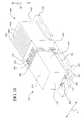
- FIG. 1is an isometric view of an interior of a receptacle connector 100 formed in accordance with an embodiment of the present invention.
- the receptacle connector 100includes a base 120 and receptacle circuit boards, or wafers 110 (although only one receptacle wafer 110 is shown in FIG. 1) having a rear portion 113 , a flex portion 112 and an interface portion 117 .
- the base 120includes an interface side 118 , side walls 116 and a rear wall 108 .
- the rear wall 108includes cover mating notches 122 having latch mating members 123 that receive and retain cover latches (not shown) formed on a cover (not shown).
- Latch members 130extend outwardly from the bottom of the base 120 at the interface side 118 .
- the latch members 130may be integrally formed with the base 120 , or they may be separate structures mounted on the base 120 .
- the base 120also includes channels 128 extending along a length thereof. Each channel 128 includes a series of receptacles 126 . Each receptacle 126 retains a compliant contact 106 . Each compliant contact 106 includes a single prong that extends down through the bottom of the base 120 , and a double prong (not shown) that extends up through the top of the base 120 .
- Each channel 128is closed by the rear wall 108 and open at the interface side 118 . At the interface side 118 , each channel 128 is positioned between flex limiting wedges 124 .
- the flex limiting wedges 124are formed such that a wide end 125 distal to the interface side 118 is wider than a tapered end 127 proximal to the interface side 118 .
- the flex limiting wedges 124may be included within an interior of a floating interface housing 620 (shown with respect to FIG. 6 ), instead of within the base 120 .
- Each channel 128receives and retains a receptacle circuit board, or wafer 110 .
- Each receptacle wafer 110includes a base mating edge (hidden by insertion of the receptacle wafer 110 into the channel 128 ) and plug mating edge 111 .
- the base mating edgehas signal and contact pads (not shown), and the plug mating edge 111 also has signal contact pads 190 , and ground contact pads (on opposite side of receptacle wafer 110 ).
- the plug mating edge 111is located at the edge of the interface portion 117 .
- Signal and ground terminals, or contact members, 22 and 12respectively, (as shown with respect to FIGS.
- the contact pads (not shown) of the base mating edgeare positioned between double prongs (not shown) of compliant contacts 106 . That is, the double prongs straddle the receptacle wafer 110 and contact it at contact pads located on the base mating edge.
- the compliant contacts 106in turn connect to a printed circuit board 102 through receptacles (not shown) formed in the printed circuit board 102 that receive and retain single prongs (not shown) of the compliant contacts 106 . Thus, an electrical path may be established between the printed circuit board 102 and the receptacle wafer 110 .
- a rear portion 113 of a receptacle wafer 110is securely retained in a channel 128 .
- the receptacle wafer 110is securely retained from the rear portion 113 to the flex portion 112 .
- Flex holes 114are formed in each receptacle wafer 110 .
- the flex holes 114are formed in one or more columns extending in a direction transverse to a length of the channels 128 .
- the area between the columns of flex holes 114is approximately the length of the flex limiting wedge 124 , such that one column of flex holes 114 is proximate to the wide end 125 of a flex limiting wedge 124 , while the other column of flex holes 114 is proximate to a tapered end 127 of the flex limiting wedge 124 .
- the receptacle wafer 110may be covered with a solder mask, the solder mask may be removed at the flex portion 112 to provide added flexibility in the flex portion 112 .
- the flex holes 114provide a weakened area in the receptacle wafer 100 such that the area between the flex holes 114 , that is the flex portion 112 , may flex easier than the rear portion 113 or the interface portion 117 of the receptacle wafer 110 . Also, copper in the flex portion 112 may be removed to provide further weakening of the flex portion 112 .
- each flex portion 112is limited by the flex limiting wedges 124 , which are positioned on either side of the receptacle wafer 110 .
- the flex limiting wedges 124may be included within the base 120 or the interior of the floating interface housing 620 . Because the tapered end 127 of each flex limiting wedge 124 is thinner than the wide end 125 , the receptacle wafer 110 may flex between the tapered ends 127 of two flex limiting wedges 124 that are positioned on either side of the receptacle wafer 110 .
- Line Adenotes the directions in which the flex portions 112 may flex, and the interface portions 117 may move.
- the flex portions 112 of the receptacle wafers 110may flex horizontally (as shown in FIG. 1 ), or in a direction perpendicular to the plane of the receptacle wafers 110 .
- the flexion of the flex portions 112is limited by the flex limiting wedges 124 .
- the movement of the interface portions 117is limited by the flex limiting wedges 124 .
- Each tapered end 127acts as a physical barrier beyond which a flex portion 112 of a receptacle wafer 110 cannot flex.
- the portion of the flex portion 112 proximate the tapered ends 127 of two flex limiting wedges 124may flex over a greater range of motion as compared to the portion of the flex portion 112 proximate the corresponding wide ends 125 . While the flex portion 112 of a receptacle wafer 100 may flex, the rear portion 113 and the interface portion 117 of the receptacle wafer 110 remain rigid and straight, relative to the flexion of the flex portion 112 . That is, the rear portion 113 is securely retained by the channel 128 , while the interface portion 117 is securely retained in interface slots of a floating interface housing 620 , as shown with respect to FIG. 6 .
- the interface portion 117moves out of the plane of the rear portion 113 in response to the flexion of the flex portion 112 . That is, while the interface portion 117 may move, it remains relatively straight and rigid, as compared to the flex portion 112 .
- FIG. 2is an isometric view of an interior of a plug connector 200 formed in accordance with an embodiment of the present invention.
- the plug connector 200includes a base 220 and plug circuit boards, or wafers 210 (although only one plug wafer 210 is shown in FIG. 2) having a rear portion 213 , a flex portion 212 and an interface portion 217 .
- the base 220includes an interface side 218 , side walls 216 and a rear wall 208 .
- the rear wall 208includes cover mating notches 222 having latch mating members 223 that receive and retain cover latches (not shown) formed on a cover (not shown).
- Latch members 230extend outwardly from the bottom of the base 220 at the interface side 218 .
- the latch members 230may be integrally formed with the base 220 , or they may be separate structures mounted on the base 220 .
- the base 220also includes channels 228 extending along a length thereof. Each channel 228 includes a series of receptacles 226 . Each receptacle 226 retains a compliant contact 206 .
- Each compliant contact 206includes a single prong (not shown) that extends down through the bottom of the base 220 , and a double prong (not shown) that extends up through the top of the base 220 .
- Each channel 228is closed by the rear wall 208 and open at the interface side 218 . At the interface side 218 , each channel 228 is positioned between flex limiting wedges 224 .
- the flex limiting wedges 224are formed such that a wide end 225 distal to the interface side 218 is wider than a tapered end 227 proximal to the interface side 218 .
- the flex limiting wedges 224may be included within an interior of a floating interface housing 720 (shown with respect to FIG. 7 ), instead of within the base 220 .
- Each channel 228receives and retains a plug circuit board, or wafer 210 .
- Each plug wafer 210includes a base mating edge (hidden by insertion of the plug wafer 210 into the channel 128 ) and plug mating edge 211 .
- the base mating edgehas signal and contact pads (not shown), while the plug mating edge 211 has signal contact pads 290 and ground contact pads 292 .
- the plug mating edge 211is located at the edge of the interface portion 217 .
- Signal and ground terminals, or contact members, 22 and 12respectively (as shown with respect to FIGS. 3 and 4) connect to contact pads 290 and 292 , respectively, on the plug mating edge 211 .
- the contact pads of the base mating edgeare positioned between double prongs (not shown) of compliant contacts 206 . That is, the double prongs straddle the plug wafer 210 and contact it at contact pads located on the base mating edge.
- the compliant contacts 206in turn connect to a printed circuit board 202 through receptacles (not shown) formed in the printed circuit board 202 that receive and retain single prongs (not shown) of the compliant contacts 206 .
- an electrical pathmay be established between the printed circuit board 202 and the plug wafer 210 .
- a rear portion 213 of a plug wafer 210is securely retained in a channel 228 .
- the plug wafer 210is securely retained from the rear portion 213 to the flex portion 212 .
- Flex holes 214are formed in each plug wafer 210 .
- the flex holes 214are formed in one or more columns extending in a direction transverse to a length of the channels 128 .
- the area between the columns of flex holes 214is approximately the length of the flex limiting wedge 224 , such that one column of flex holes 214 is proximate to the wide end 225 of the flex limiting wedge 224 , while the other column of flex holes 214 is proximate to the tapered end 227 of the flex limiting wedge 224 .
- the plug wafer 210may be covered with a solder mask, the solder mask may be removed at the flex portion 212 to provide added flexibility in the flex portion 212 . Additionally, the flex holes 214 provide a weakened area in the plug wafer 210 such that the area between the flex holes 214 , that is the flex portion 212 , may flex easier than the rear portion 213 or the interface portion 217 of the plug wafer 210 .
- each flex portion 212The flexion of each flex portion 212 is limited by the flex limiting wedges 224 , which are positioned on either side of the plug wafer 210 . Because the tapered end 227 of each flex limiting wedge 224 is thinner than the wide end 225 , the plug wafer 210 may flex between the tapered ends 227 of two flex limiting wedges 224 that are positioned on either side of the plug wafer 210 .
- Line Bdenotes the directions in which the flex portions 212 may flex, and the interface portions 217 may move. That is, the flex portions 212 of the plug wafers 210 may flex vertically (as shown in FIG. 1 ), or in a direction perpendicular to the plane of the plug wafers 210 .
- the flexion of the flex portions 212is limited by the flex limiting wedges 224 .
- Each tapered end 227acts as a physical barrier beyond which the receptacle wafer 210 cannot flex.
- the portion of the flex portion 212 proximate the tapered ends 227 of two flex limiting wedges 224may flex over a wider range of motion as compared to the portion of the flex portion 212 proximate the corresponding wide ends 225 due to the tapered nature of the flex limiting wedges 224 . While the flex portion 212 of a plug wafer 210 may flex, the rear portion 213 and the interface portion 217 of the plug wafer 210 remain rigid and fixed.
- the rear portion 213is securely retained by the channel 228 , while the interface portion 217 is securely retained in interface slots of a floating interface housing 720 .
- the interface portion 217moves out of the plane of the rear portion 213 in response to the flexion of the flex portion 212 . That is, while the interface portion 217 may move, it remains relatively straight and rigid, as compared to the flex portion 212 .
- FIG. 3is an isometric view of a ground terminal, or ground contact member, 12 formed in accordance with an embodiment of the present invention.
- the ground terminal 12includes a single beam receptacle interconnect 14 on one end of an intermediate portion 16 and a plug ground interconnect 18 shaped like a tuning fork on the opposite end.
- the plug ground interconnect 18includes two prongs 2 and 4 . Therefore one prong 2 of the plug ground interconnect 18 contacts a ground contact pad 292 on one side of the plug wafer 210 while the other prong 4 of the plug ground interconnect 18 contacts a ground contact pad 292 on the other side of the plug wafer 210 . That is, the plug wafer 210 is straddled by receptacle ground interconnects 18 .
- the single beam receptacle interconnect 14contacts a ground contact pad (not shown) located on one side of the receptacle wafer 110 .
- FIG. 4is an isometric view of a signal terminal, or signal contact member, 22 formed in accordance with an embodiment of the present invention.
- the signal terminal 22includes a double beam receptacle interconnect 24 on one side of an intermediate portion 26 and a plug signal interconnect 28 shaped like a tuning fork on the opposite end.
- the plug signal interconnect 28includes two prongs 3 and 5 . Therefore one prong 3 of the plug signal interconnect 28 contacts a signal contact pad 290 on one side of the plug wafer 210 while the other prong of the plug signal interconnect 28 contacts a signal contact pad 290 on the other side of the plug wafer 210 . That is, the plug wafer 210 is straddled by the plug signal interconnect 28 .
- the double beam receptacle interconnect 24contacts a signal contact pad 190 located on one side of the receptacle wafer 110 . That is, both beams of the receptacle interconnect 24 contact one signal contact pad 190 located on one side of the receptacle wafer 110 .
- FIG. 5is an isometric interior view of a receptacle wafer 110 orthogonally mated with a plug wafer 210 according to an embodiment of the present invention.
- the signal terminal 22through the double beam receptacle interconnect 24 , engages a signal contact pad 190 on the receptacle wafer 110 on a first side
- the ground terminal 12through the single beam receptacle interconnect 14 engages a ground contact pad (on hidden side of receptacle wafer 110 ) on the same receptacle wafer 110 on a second side.
- the plug signal interconnect 28through the prongs 3 and 5 , straddles the plug wafer 210 such that the signal terminal 22 engages signal contact pads 290 on both sides of the plug wafer 210 .
- the plug ground interconnect 18through the prongs 2 and 4 , straddles the plug wafer 210 such that the ground terminal 12 engages ground contact pads 292 on both sides of the plug wafer 210 .
- the receptacle wafer 110is positioned between a plurality of signal terminals 22 on one side of the receptacle wafer 110 and a plurality of ground terminals 12 on a second side of the receptacle wafer 110 .
- a plug wafer 210is positioned between a plurality of signal and ground terminals 22 and 12 , each of which contacts the plug wafer 210 on both sides.
- FIG. 8illustrates a top view of a receptacle wafer 110 mated with a plug wafer 210 according to an embodiment of the present invention.
- FIG. 8 ashows a receptacle wafer 110 in a substantially straight alignment. That is, no lateral forces are warping the receptacle wafer 110 , or forcing the flex portion 112 to flex.
- FIGS. 8 b and 8 chowever, lateral forces (F) are exerted on the receptacle wafer 110 .
- the movement of the signal terminal 22 and ground terminalis exaggerated to better show the movement of the flex portion 112 .
- FIG. 9illustrates a side view of a receptacle wafer 110 mating with a plug wafer 210 according to an embodiment of the present invention.
- FIG. 9most of the supporting structure, such as the flex limiting wedges 124 and 224 , is not shown.
- FIG. 9 ashows a plug wafer 210 in a substantially straight alignment. That is, no upward or downward forces are warping the plug wafer 210 , or forcing the flex portion 212 to flex. As in FIG. 8, the movement in FIG. 9 is exaggerated.
- FIGS. 9 b and 9 cupward and downward forces are exerted on the plug wafer 210 . The forces cause the signal terminal 22 and the ground terminal 12 (ground terminal 12 hidden in FIG.
- Prongs 3 , 5 and 2 , 4may also flex.
- the prongs 3 , 5 and 2 , 4may flex by an amount depending on the flex of the flex portion 212 .
- FIGS. 8 b and 8 conly the flex portion 212 flexes, while the rear and interface portions 213 , 217 of the plug wafer 210 remain in a straight alignment. However, the interface portion 217 moves (but does not flex) relative to the rear portion 213 in response to the flexion of the flex portion 212 .
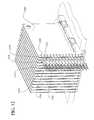
- FIG. 6is an isometric view of a receptacle connector 100 , without receptacle wafers 110 , formed in accordance with an embodiment of the present invention.
- the receptacle connectorincludes the base 120 , a floating interface housing 620 and a cover 610 .
- the floating interface housing 620has latch recesses 650 having latch projections 652 protruding therefrom and latch flexion limiting lips 660 .
- the floating interface housing 620also includes side walls 622 , a top wall 624 , a wafer projection wall 630 and a bottom wall 626 , which define an interface cavity 628 .
- the latch recesses 650 and latch projections 652are formed on the exterior of the top wall 624 and the bottom wall 626 .
- the wafer projection wall 630includes slots 632 extending from the top wall 624 to the bottom wall 626 .
- the slots 632allow the receptacle wafers 110 to pass through.
- the side of the bottom wall 626 within the interface cavity 628includes guide slots 640 that receive and securely retain lower edges of the interface portions 117 of the receptacle wafers 110 .
- the side of the top wall 624 facing the interface cavity 628may also include guide slots that receive and securely retain upper edges of the interface portions 117 of the receptacle wafers 110 .
- each receptacle wafer 110flexes, while the rear portion 113 and the interface portion 117 remain relatively rigid and straight as compared to the flex portion 112 .
- the interface portion 117moves in response to the flexing of the flex portion 112 .
- the cover 610includes a top wall 612 , side walls 616 , a rear wall 614 , latch members 130 and cover latches 642 .
- An open cavity(not shown) is defined by the walls 612 , 616 and 614 .
- the latch mating members 123 and cover mating notches 122are formed on the side walls 116 of the base 120 . As shown in FIG. 1, however, the latch mating members 123 and cover mating notches 122 may be formed on the rear wall 108 of the base 120 . Alternatively, these features may be located on the side walls 116 and the rear wall 108 .
- the cover latches 642are oriented on the cover 610 to correspond to the position(s) of the cover mating notches 122 and the latch mating members 123 .
- the cover latches 642are received by the cover mating notches 122 and retained by the latch mating members 123 .
- the cover 122may be fastened to the base 120 through screws, glue, and the like.
- the latch members 130may be integrally formed with the top wall 612 of the cover 610 , or they may be separately mounted on the top wall 612 .
- the latch members 130 on the cover 610 and on the base 120have a flex end 656 and a retained end 654 .
- the latch members 130engage the latch recesses 650 and mate with the latch projections 652 .
- the retained ends 654which are retained by the latch recesses 650 , remain fixed while the flex ends 656 may move, relative to the actual movement of the floating interface housing 620 , in the directions denoted by line A. That is, the flex ends 656 , because they are connected or formed integrally with the stationary cover 610 or base 120 , do not actually move.
- the floating interface housing 620moves, which produces relative motion between the flex ends 656 and the floating interface housing 620 .
- the movement of the flex ends 656is limited by the latch flexion limiting lips 660 , which form a barrier that impedes continued movement of the latch members 130 .
- FIG. 14is an isometric view of a latching system formed in accordance with an embodiment of the present invention.
- the latching system shown in FIG. 14may be used with the receptacle connector 100 and/or the plug connector 200 .
- the latch recesses 650include clearance areas 662 defined between side walls 668 of the latch members 130 and the latch flexion limiting lips 660 .
- the clearance areas 662provide an area over which the latch members 130 may move in relation to the floating interface 620 .
- the clearance areas 662are wider proximate the flex ends 654 of the latch members as compared to the retained areas 656 . That is, the latch members 130 are more securely retained at their retained ends 656 as compared to their flex ends 654 .
- the floating interface housing 620moves in response to the movement of the flex portions 112 of the receptacle wafers 110 . That is, movement of the floating interface housing 620 through the clearance areas 662 causes a corresponding relative movement in the latch members 130 . That is, the cover 610 and base 120 remain stationary while the floating interface housing 620 moves. Movement between the latch member 130 and the latch flexion limiting lips 660 is relative to the actual movement of the floating interface housing 620 . However, relative movement of the latch member 130 is limited by the latch flexion limiting lips 660 . That is, as the latch members 130 contact the latch flexion limiting lips 660 , continued movement of the floating interface 620 in that direction is arrested.
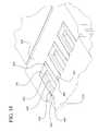
- FIG. 7is an isometric view of a plug connector 200 , without plug wafers 110 , formed in accordance with an embodiment of the present invention.
- the plug connector 200includes the base 220 , a floating interface housing 720 and a cover 710 .
- the floating interface housing 720has latch recesses 750 having latch projections 752 , latch flexion limiting lips 760 , side walls 722 , a top wall 724 , a bottom wall 726 and an interface wall 728 .
- the latch recesses 750 and latch projections 752are formed on the exterior of the top wall 724 and the bottom wall 726 .
- At least one of the side walls 722includes slots 732 extending from the interface wall 728 .
- each plug wafer 210is fixed at its rear portion 213 and its interface portion 217 . Only the flex portion 212 of each plug wafer 210 flexes, while the rear portion 213 and the interface portion 217 remain relatively rigid and straight as compared to the flex portion 212 . However, as mentioned above, while the interface portion 217 remains in a straight orientation, the interface portion 217 moves in response to the flexing of the flex portion 112 .
- the plug wafers 210do not pass through the interface wall 728 .
- the interface wall 728includes guide members 780 that support and align the single beam receptacle interconnects 14 of the ground terminals 22 and the double beam receptacle interconnects 24 of the signal terminals 22 so that they may pass through channels 778 formed within the interface wall 728 .
- the single beam receptacle interconnects 14 and the double beam receptacle interconnects 24are exposed and may mate with contact pads on receptacle wafers 110 when the plug connector 200 mates with the receptacle connector 100 .
- the cover 710includes a top wall 712 , side walls 716 , a rear wall 714 , latch members 230 and cover latches 742 .
- An open cavity(not shown) is defined by the walls 712 , 716 and 714 .
- the latch mating members 223 and cover mating notches 222are formed on the side walls 216 of the base 220 . As shown in FIG. 2, however, the latch mating members 223 and cover mating notches 222 may be formed on the rear wall 208 of the base 220 . Alternatively, these features may be located on the side walls 216 and the rear wall 208 .
- the cover latches 742are oriented on the cover 710 to correspond to the position(s) of the cover mating notches 222 and the latch mating members 223 .
- the cover latches 742are received by the cover mating notches 222 and retained by the latch mating members 223 .
- the cover 222may be fastened to the base 220 through screws, glue, and the like.
- the latch members 230may be integrally formed with the top wall 712 of the cover 710 , or they may be separately mounted on the top wall 712 .
- the latch members 230 on the cover 710 and on the base 220have a flex end 754 and a retained end 756 .
- the latch members 230engage the latch recesses 750 and mate with the latch projections 752 .
- the retained ends 756which are retained by the latch recesses 750 , remain fixed while the flex ends 754 may move, relative to the actual movement of the floating interface housing 720 , in the directions denoted by line B. That is, the flex ends 754 , because they are connected, or formed integrally with the stationary cover 710 or base 220 , do not actually move.
- the floating interface housing 720moves, which produces relative motion between the flex ends 754 and the floating interface housing 720 .
- the movement of the flex ends 754is limited by the latch flexion limiting lips 760 .
- the movement of the latching system used with the plug connector 200is similar to that used with the receptacle connector 100 .
- the movement of the floating interface housing 720causes the flex ends 754 of the latch members 230 to contact the latch flexion limiting lips 760 , continued movement of the floating interface in that direction is arrested.
- the receptacle connector 100is mated with the plug connector 200 so that electrical signals may travel from plug wafers 210 to receptacle wafers 110 , and vice versa. That is, the receptacle connector 100 receives and snapably retains the plug connector 200 , such that the receptacle wafers 110 orthogonally mate with the plug wafers 210 , as shown in FIG. 5 .
- the mating of the receptacle connector 100 with the plug connector 200provides contact alignment correction over all angles and orientations because the floating interface 620 of the receptacle connector 100 may move over a horizontal plane (denoted by line A) and the floating interface 720 of the plug connector 200 may move over a vertical plane (denoted by line B).
- vertical misalignment, horizontal misalignment, or combinations of bothmay be corrected through the floating interface housings 620 and 720 of the receptacle and plug connectors 100 and 200 , respectively.
- FIG. 10is an isometric view of the receptacle connector 100 mating in a coplanar fashion with a plug connector 1000 , according to an embodiment of the present invention.
- the plug connector 1000includes many of the same features as the plug connector 200 , as described above, except it has wafer slots 1002 formed on a top housing 1016 of the cover 1010 . Alternatively, the wafer slots 1002 may not be included within the top housing 1016 . The wafer slots 1002 assist in retaining the plug wafers (not shown).
- Both the receptacle wafers 110 and the plug wafersare aligned in a coplanar fashion. That is, the receptacle wafer 110 that mates with its corresponding plug wafer is initially aligned in the same plane as the plug wafer.
- the interface housing 620 of the receptacle connector 100may move in the directions denoted by Line A, while the interface housing (covered by the interface housing 620 of the receptacle connector 100 ) of the plug housing 1000 may move in the directions denoted by Line B.
- FIG. 11is an isometric view of a plug connector 1000 according to an embodiment of the present invention.
- the plug connector 1000does not have the wafer slots formed in the top housing 1016 of the cover 1010 . Rather, wafer slots 1102 are formed in the floating interface housing 1120 .
- the plug connector 1000includes an alternative latching system.
- the floating interface housing 1120includes a latching recess 1142 and a latching projection 1144 .
- the cover 1010includes a latching member 1132 having a flex end 1134 and a retained end 1136 . The movement of the latching member 1132 and the latching projection 1144 function in a similar way as those described above with respect to FIGS. 1-9.
- the floating interface 1120also includes a float-limiting divot 1150 and a float-limiting wall 1152 .
- the latching member 1132includes an abutting member 1160 that may move through the float-limiting divot 1150 until it abuts the floating limiting wall 1152 .
- the movement of the latching member 1132is limited by the float limiting walls 1152 .
- a stationary intermediate piece 1188may be used to ensure that the cover 1010 does not move.
- the alternative latching system shown in FIG. 11may also be used with the receptacle connector 100 or the plug connector 200 .
- a guide track systemmay be used in which an interface housing includes guide track(s) and the corresponding cover includes channel(s) that receive the guide track. The interface housing may then slide along the channel(s) on the guide tracks(s).
- stop blocksmay be positioned on the guide track(s) and/or channel(s) that limit the movement of the interface housing.
- the guide tracksmay either be smooth or include a gear system in which the guide track has gear teeth that are engaged by a gear, or cog.
- fastenerssuch as screws, may be used.
- the interface housingmay be screwed to the cover such that the interface housing may move over the cover.
- the interface housingmay be screwed to the cover at a mid point of the top wall of the interface housing, and the interface housing may be screwed to the base at a mid point of the bottom wall of the interface housing.
- the two screwswould be positioned along the same axis, thereby providing a rotational axis over which the interface housing may move.
- a clearance area between the interface housing and the covermay also be used to provide additional range of motion.
- FIG. 12is an isometric view of an interior of the plug connector 1000 according to an embodiment of the present invention.
- the plug wafers 1200are connected to signal terminals 1222 and ground terminals 1212 .
- Each signal terminal 1222includes a double beam receptacle interconnect 1224 extending from an intermediate portion 1226 , and a single beam plug signal interconnect 1228 extending from an opposite end of the intermediate portion 1226 .
- Each double beam receptacle interconnect 1224connects to one side of a receptacle wafer (not shown), while each single beam plug signal interconnect 1228 connects to one side of a plug wafer 1200 .
- Each ground terminal 1212includes a single beam receptacle interconnect 1214 extending from an intermediate portion 1216 connecting to a second side of a receptacle wafer (not shown) and a wide plug ground interconnect 1218 , which connects to one side of a plug wafer 1200 .
- the plug ground interconnectis wider than the plug signal interconnect 1228 .
- FIG. 13is a side view illustrating movement of signal and ground terminals 1222 and 1212 during an upward shift of a receptacle wafer 110 , according to an embodiment of the present invention.
- the plug signal interconnect 1228when a receptacle wafer moves, for example, in the up direction, and the plug wafer 1200 remains stationary, the plug signal interconnect 1228 , the movement of which is limited by stop blocks 1302 , pivots, in a cantilever fashion, due to the movement of the receptacle wafer 110 .
- the stop blocks 1302may be formations that outwardly extend from the plug wafer 1200 .
- a retained end 1260 of a plug signal interconnect 1228engages a signal contact pad 1261 , which is positioned between two stop blocks 1302 .
- the retained end 1260is positioned between two signal blocks 1302 .
- the movement of the receptacle wafer 110shifts the plug signal interconnect 1228 out of a level orientation.
- the ground terminal 1212remains in a level orientation because the ground terminal 1212 slides up or down on the plug wafer 1200 in response to the movement of the receptacle wafer 110 .
- the plug ground interconnect 1218is wider than the plug signal interconnect 1228 , the plug ground interconnect 1218 is able to shield the plug signal interconnect 1228 from other plug signal interconnects 1228 despite the cantilever movement of the plug signal interconnects 1228 .
- certain embodiments of the present inventionprovide an electrical connector that maintains proper contact between electrical wafers included within a first connector and those in a second connector, whether the wafers of the first connector mate orthogonally, or in a coplanar fashion with those of thee second connector. Further, certain embodiments of the present invention provide an electrical connector that maintains proper alignment and corrects misalignments between circuit boards, or wafers, within a first connector and those of a second connector housing.
Landscapes
- Details Of Connecting Devices For Male And Female Coupling (AREA)
- Multi-Conductor Connections (AREA)
- Coupling Device And Connection With Printed Circuit (AREA)
Abstract
Description
Claims (35)
Priority Applications (6)
| Application Number | Priority Date | Filing Date | Title |
|---|---|---|---|
| US10/042,635US6663426B2 (en) | 2002-01-09 | 2002-01-09 | Floating interface for electrical connector |
| EP02795919AEP1466391A1 (en) | 2002-01-09 | 2002-12-19 | Floating interface for electrical connector |
| CNB028270134ACN1286217C (en) | 2002-01-09 | 2002-12-19 | Floating interface for electrical connector |
| AU2002360646AAU2002360646A1 (en) | 2002-01-09 | 2002-12-19 | Floating interface for electrical connector |
| JP2003561054AJP2005515608A (en) | 2002-01-09 | 2002-12-19 | Floating fitting for electrical connectors |
| PCT/US2002/040448WO2003061079A1 (en) | 2002-01-09 | 2002-12-19 | Floating interface for electrical connector |
Applications Claiming Priority (1)
| Application Number | Priority Date | Filing Date | Title |
|---|---|---|---|
| US10/042,635US6663426B2 (en) | 2002-01-09 | 2002-01-09 | Floating interface for electrical connector |
Publications (2)
| Publication Number | Publication Date |
|---|---|
| US20030129878A1 US20030129878A1 (en) | 2003-07-10 |
| US6663426B2true US6663426B2 (en) | 2003-12-16 |
Family
ID=21922957
Family Applications (1)
| Application Number | Title | Priority Date | Filing Date |
|---|---|---|---|
| US10/042,635Expired - LifetimeUS6663426B2 (en) | 2002-01-09 | 2002-01-09 | Floating interface for electrical connector |
Country Status (6)
| Country | Link |
|---|---|
| US (1) | US6663426B2 (en) |
| EP (1) | EP1466391A1 (en) |
| JP (1) | JP2005515608A (en) |
| CN (1) | CN1286217C (en) |
| AU (1) | AU2002360646A1 (en) |
| WO (1) | WO2003061079A1 (en) |
Cited By (53)
| Publication number | Priority date | Publication date | Assignee | Title |
|---|---|---|---|---|
| US20040018773A1 (en)* | 2002-07-29 | 2004-01-29 | Fci Americas Technology, Inc. | Printed circuit board assembly having a BGA connection |
| US6808419B1 (en)* | 2003-08-29 | 2004-10-26 | Hon Hai Precision Ind. Co., Ltd. | Electrical connector having enhanced electrical performance |
| US20050020134A1 (en)* | 2003-07-24 | 2005-01-27 | Winings Clifford L. | Modular electrical connector |
| US20050048817A1 (en)* | 2003-09-03 | 2005-03-03 | Cohen Thomas S. | High speed, high density electrical connector |
| US6884117B2 (en)* | 2003-08-29 | 2005-04-26 | Hon Hai Precision Ind. Co., Ltd. | Electrical connector having circuit board modules positioned between metal stiffener and a housing |
| US6932649B1 (en)* | 2004-03-19 | 2005-08-23 | Tyco Electronics Corporation | Active wafer for improved gigabit signal recovery, in a serial point-to-point architecture |
| US6986682B1 (en)* | 2005-05-11 | 2006-01-17 | Myoungsoo Jeon | High speed connector assembly with laterally displaceable head portion |
| US20060057897A1 (en)* | 2004-09-14 | 2006-03-16 | Fci Americas Technology, Inc. | Ball grid array connector |
| US7226296B2 (en) | 2004-12-23 | 2007-06-05 | Fci Americas Technology, Inc. | Ball grid array contacts with spring action |
| US7303427B2 (en) | 2005-04-05 | 2007-12-04 | Fci Americas Technology, Inc. | Electrical connector with air-circulation features |
| US20080108233A1 (en)* | 2006-11-07 | 2008-05-08 | Myoungsoo Jeon | Connector having self-adjusting surface-mount attachment structures |
| US7384289B2 (en) | 2005-01-31 | 2008-06-10 | Fci Americas Technology, Inc. | Surface-mount connector |
| US7402064B2 (en) | 2003-12-31 | 2008-07-22 | Fci Americas Technology, Inc. | Electrical power contacts and connectors comprising same |
| US7425145B2 (en) | 2006-05-26 | 2008-09-16 | Fci Americas Technology, Inc. | Connectors and contacts for transmitting electrical power |
| US20080261417A1 (en)* | 2007-04-18 | 2008-10-23 | Fci Americas Technology, Inc. | Low profile electrical connector |
| US7458839B2 (en) | 2006-02-21 | 2008-12-02 | Fci Americas Technology, Inc. | Electrical connectors having power contacts with alignment and/or restraining features |
| US7476108B2 (en) | 2004-12-22 | 2009-01-13 | Fci Americas Technology, Inc. | Electrical power connectors with cooling features |
| USD606496S1 (en) | 2009-01-16 | 2009-12-22 | Fci Americas Technology, Inc. | Right-angle electrical connector |
| USD606497S1 (en) | 2009-01-16 | 2009-12-22 | Fci Americas Technology, Inc. | Vertical electrical connector |
| US7641500B2 (en) | 2007-04-04 | 2010-01-05 | Fci Americas Technology, Inc. | Power cable connector system |
| USD608293S1 (en) | 2009-01-16 | 2010-01-19 | Fci Americas Technology, Inc. | Vertical electrical connector |
| USD610548S1 (en) | 2009-01-16 | 2010-02-23 | Fci Americas Technology, Inc. | Right-angle electrical connector |
| USRE41283E1 (en) | 2003-01-28 | 2010-04-27 | Fci Americas Technology, Inc. | Power connector with safety feature |
| US7726982B2 (en) | 2006-06-15 | 2010-06-01 | Fci Americas Technology, Inc. | Electrical connectors with air-circulation features |
| USD618180S1 (en) | 2009-04-03 | 2010-06-22 | Fci Americas Technology, Inc. | Asymmetrical electrical connector |
| USD618181S1 (en) | 2009-04-03 | 2010-06-22 | Fci Americas Technology, Inc. | Asymmetrical electrical connector |
| USD619099S1 (en) | 2009-01-30 | 2010-07-06 | Fci Americas Technology, Inc. | Electrical connector |
| US7762857B2 (en) | 2007-10-01 | 2010-07-27 | Fci Americas Technology, Inc. | Power connectors with contact-retention features |
| US7905731B2 (en) | 2007-05-21 | 2011-03-15 | Fci Americas Technology, Inc. | Electrical connector with stress-distribution features |
| USD640637S1 (en) | 2009-01-16 | 2011-06-28 | Fci Americas Technology Llc | Vertical electrical connector |
| US8062051B2 (en) | 2008-07-29 | 2011-11-22 | Fci Americas Technology Llc | Electrical communication system having latching and strain relief features |
| USD664096S1 (en) | 2009-01-16 | 2012-07-24 | Fci Americas Technology Llc | Vertical electrical connector |
| US8323049B2 (en) | 2009-01-30 | 2012-12-04 | Fci Americas Technology Llc | Electrical connector having power contacts |
| USD718253S1 (en) | 2012-04-13 | 2014-11-25 | Fci Americas Technology Llc | Electrical cable connector |
| US8905651B2 (en) | 2012-01-31 | 2014-12-09 | Fci | Dismountable optical coupling device |
| USD720698S1 (en) | 2013-03-15 | 2015-01-06 | Fci Americas Technology Llc | Electrical cable connector |
| US8944831B2 (en) | 2012-04-13 | 2015-02-03 | Fci Americas Technology Llc | Electrical connector having ribbed ground plate with engagement members |
| USD727268S1 (en) | 2012-04-13 | 2015-04-21 | Fci Americas Technology Llc | Vertical electrical connector |
| USD727852S1 (en) | 2012-04-13 | 2015-04-28 | Fci Americas Technology Llc | Ground shield for a right angle electrical connector |
| US9048583B2 (en) | 2009-03-19 | 2015-06-02 | Fci Americas Technology Llc | Electrical connector having ribbed ground plate |
| US9065215B2 (en) | 2011-02-18 | 2015-06-23 | Fci Americas Technology Llc | Electrical connector having common ground shield |
| USD733662S1 (en) | 2013-01-25 | 2015-07-07 | Fci Americas Technology Llc | Connector housing for electrical connector |
| US20150194755A1 (en)* | 2014-01-08 | 2015-07-09 | Tyco Electronics Corporation | Connector assembly |
| USD746236S1 (en) | 2012-07-11 | 2015-12-29 | Fci Americas Technology Llc | Electrical connector housing |
| US9257778B2 (en) | 2012-04-13 | 2016-02-09 | Fci Americas Technology | High speed electrical connector |
| US9419356B2 (en) | 2013-03-14 | 2016-08-16 | Fci Americas Technology Llc | Electrical power contact with two adjacent contact blades abutting each other |
| US9543703B2 (en) | 2012-07-11 | 2017-01-10 | Fci Americas Technology Llc | Electrical connector with reduced stack height |
| US10965062B1 (en) | 2020-03-26 | 2021-03-30 | TE Connectivity Services Gmbh | Modular electrical connector with conductive coating to reduce crosstalk |
| US10998678B1 (en) | 2020-03-26 | 2021-05-04 | TE Connectivity Services Gmbh | Modular electrical connector with additional grounding |
| US11025014B1 (en) | 2020-03-26 | 2021-06-01 | TE CONNECTNITY SERVICES GmbH | Shield component for use with modular electrical connector to reduce crosstalk |
| US11031734B1 (en) | 2020-03-26 | 2021-06-08 | TE Connectivity Services Gmbh | Modular electrical connector with reduced crosstalk |
| US11264749B2 (en) | 2020-03-26 | 2022-03-01 | TE Connectivity Services Gmbh | Modular connector with printed circuit board wafer to reduce crosstalk |
| US11297712B2 (en) | 2020-03-26 | 2022-04-05 | TE Connectivity Services Gmbh | Modular printed circuit board wafer connector with reduced crosstalk |
Families Citing this family (4)
| Publication number | Priority date | Publication date | Assignee | Title |
|---|---|---|---|---|
| CN101873781B (en)* | 2010-06-28 | 2012-01-04 | 华为技术有限公司 | Plug-in mechanism, finished board with same and plug-in frame |
| US8804342B2 (en)* | 2012-02-22 | 2014-08-12 | Tyco Electronics Corporation | Communication modules having connectors on a leading end and systems including the same |
| CN110311241A (en) | 2019-06-24 | 2019-10-08 | 番禺得意精密电子工业有限公司 | Electric connector |
| US20240186734A1 (en)* | 2022-12-06 | 2024-06-06 | Amphenol Corporation | Card connector |
Citations (5)
| Publication number | Priority date | Publication date | Assignee | Title |
|---|---|---|---|---|
| US299483A (en)* | 1884-05-27 | William lang | ||
| US5951315A (en) | 1996-02-15 | 1999-09-14 | Japan Aviation Electronics Industry, Ltd. | Electrical connector of a turn contact type which is simple in shape |
| US6309223B1 (en) | 2000-06-13 | 2001-10-30 | Trw Inc. | Terminal assembly for flexible circuit strip |
| US6347950B1 (en) | 2000-09-14 | 2002-02-19 | Smk Corporation | Floating connector |
| US6347962B1 (en) | 2001-01-30 | 2002-02-19 | Tyco Electronics Corporation | Connector assembly with multi-contact ground shields |
Family Cites Families (2)
| Publication number | Priority date | Publication date | Assignee | Title |
|---|---|---|---|---|
| US4954086A (en)* | 1989-06-21 | 1990-09-04 | Burndy Corporation | Float/guide member for card edge connector |
| US5415559A (en)* | 1992-05-18 | 1995-05-16 | Japan Aviation Electronics Industry, Ltd. | Electrical connector having a plurality of contact pin springs |
- 2002
- 2002-01-09USUS10/042,635patent/US6663426B2/ennot_activeExpired - Lifetime
- 2002-12-19WOPCT/US2002/040448patent/WO2003061079A1/enactiveApplication Filing
- 2002-12-19EPEP02795919Apatent/EP1466391A1/ennot_activeWithdrawn
- 2002-12-19CNCNB028270134Apatent/CN1286217C/ennot_activeExpired - Fee Related
- 2002-12-19AUAU2002360646Apatent/AU2002360646A1/ennot_activeAbandoned
- 2002-12-19JPJP2003561054Apatent/JP2005515608A/enactivePending
Patent Citations (5)
| Publication number | Priority date | Publication date | Assignee | Title |
|---|---|---|---|---|
| US299483A (en)* | 1884-05-27 | William lang | ||
| US5951315A (en) | 1996-02-15 | 1999-09-14 | Japan Aviation Electronics Industry, Ltd. | Electrical connector of a turn contact type which is simple in shape |
| US6309223B1 (en) | 2000-06-13 | 2001-10-30 | Trw Inc. | Terminal assembly for flexible circuit strip |
| US6347950B1 (en) | 2000-09-14 | 2002-02-19 | Smk Corporation | Floating connector |
| US6347962B1 (en) | 2001-01-30 | 2002-02-19 | Tyco Electronics Corporation | Connector assembly with multi-contact ground shields |
Cited By (89)
| Publication number | Priority date | Publication date | Assignee | Title |
|---|---|---|---|---|
| US20040018773A1 (en)* | 2002-07-29 | 2004-01-29 | Fci Americas Technology, Inc. | Printed circuit board assembly having a BGA connection |
| US7413450B2 (en) | 2002-07-29 | 2008-08-19 | Fci Americas Technology, Inc. | Printed circuit board assembly having a BGA connection |
| US20060128184A1 (en)* | 2002-07-29 | 2006-06-15 | Fci Americas Technology, Inc. | Printed circuit board assembly having a BGA connection |
| USRE41283E1 (en) | 2003-01-28 | 2010-04-27 | Fci Americas Technology, Inc. | Power connector with safety feature |
| US20050020134A1 (en)* | 2003-07-24 | 2005-01-27 | Winings Clifford L. | Modular electrical connector |
| US7059907B2 (en)* | 2003-07-24 | 2006-06-13 | Fci Americas Technology, Inc. | Modular electrical connector |
| US6884117B2 (en)* | 2003-08-29 | 2005-04-26 | Hon Hai Precision Ind. Co., Ltd. | Electrical connector having circuit board modules positioned between metal stiffener and a housing |
| US6808419B1 (en)* | 2003-08-29 | 2004-10-26 | Hon Hai Precision Ind. Co., Ltd. | Electrical connector having enhanced electrical performance |
| US7074086B2 (en)* | 2003-09-03 | 2006-07-11 | Amphenol Corporation | High speed, high density electrical connector |
| US20050048817A1 (en)* | 2003-09-03 | 2005-03-03 | Cohen Thomas S. | High speed, high density electrical connector |
| US7690937B2 (en) | 2003-12-31 | 2010-04-06 | Fci Americas Technology, Inc. | Electrical power contacts and connectors comprising same |
| US7775822B2 (en) | 2003-12-31 | 2010-08-17 | Fci Americas Technology, Inc. | Electrical connectors having power contacts with alignment/or restraining features |
| US8062046B2 (en) | 2003-12-31 | 2011-11-22 | Fci Americas Technology Llc | Electrical power contacts and connectors comprising same |
| US8187017B2 (en) | 2003-12-31 | 2012-05-29 | Fci Americas Technology Llc | Electrical power contacts and connectors comprising same |
| US7452249B2 (en) | 2003-12-31 | 2008-11-18 | Fci Americas Technology, Inc. | Electrical power contacts and connectors comprising same |
| US7862359B2 (en) | 2003-12-31 | 2011-01-04 | Fci Americas Technology Llc | Electrical power contacts and connectors comprising same |
| US7402064B2 (en) | 2003-12-31 | 2008-07-22 | Fci Americas Technology, Inc. | Electrical power contacts and connectors comprising same |
| US6932649B1 (en)* | 2004-03-19 | 2005-08-23 | Tyco Electronics Corporation | Active wafer for improved gigabit signal recovery, in a serial point-to-point architecture |
| US20060057897A1 (en)* | 2004-09-14 | 2006-03-16 | Fci Americas Technology, Inc. | Ball grid array connector |
| US7214104B2 (en) | 2004-09-14 | 2007-05-08 | Fci Americas Technology, Inc. | Ball grid array connector |
| US7476108B2 (en) | 2004-12-22 | 2009-01-13 | Fci Americas Technology, Inc. | Electrical power connectors with cooling features |
| US7226296B2 (en) | 2004-12-23 | 2007-06-05 | Fci Americas Technology, Inc. | Ball grid array contacts with spring action |
| US7384289B2 (en) | 2005-01-31 | 2008-06-10 | Fci Americas Technology, Inc. | Surface-mount connector |
| US7749009B2 (en) | 2005-01-31 | 2010-07-06 | Fci Americas Technology, Inc. | Surface-mount connector |
| US7541135B2 (en) | 2005-04-05 | 2009-06-02 | Fci Americas Technology, Inc. | Power contact having conductive plates with curved portions contact beams and board tails |
| US7303427B2 (en) | 2005-04-05 | 2007-12-04 | Fci Americas Technology, Inc. | Electrical connector with air-circulation features |
| US6986682B1 (en)* | 2005-05-11 | 2006-01-17 | Myoungsoo Jeon | High speed connector assembly with laterally displaceable head portion |
| US7458839B2 (en) | 2006-02-21 | 2008-12-02 | Fci Americas Technology, Inc. | Electrical connectors having power contacts with alignment and/or restraining features |
| US7425145B2 (en) | 2006-05-26 | 2008-09-16 | Fci Americas Technology, Inc. | Connectors and contacts for transmitting electrical power |
| US7726982B2 (en) | 2006-06-15 | 2010-06-01 | Fci Americas Technology, Inc. | Electrical connectors with air-circulation features |
| US7413451B2 (en) | 2006-11-07 | 2008-08-19 | Myoungsoo Jeon | Connector having self-adjusting surface-mount attachment structures |
| US20080108233A1 (en)* | 2006-11-07 | 2008-05-08 | Myoungsoo Jeon | Connector having self-adjusting surface-mount attachment structures |
| US7641500B2 (en) | 2007-04-04 | 2010-01-05 | Fci Americas Technology, Inc. | Power cable connector system |
| US20080261417A1 (en)* | 2007-04-18 | 2008-10-23 | Fci Americas Technology, Inc. | Low profile electrical connector |
| US7815444B2 (en)* | 2007-04-18 | 2010-10-19 | Fci Americas Technology, Inc. | Low profile electrical connector |
| US7905731B2 (en) | 2007-05-21 | 2011-03-15 | Fci Americas Technology, Inc. | Electrical connector with stress-distribution features |
| US7762857B2 (en) | 2007-10-01 | 2010-07-27 | Fci Americas Technology, Inc. | Power connectors with contact-retention features |
| US8062051B2 (en) | 2008-07-29 | 2011-11-22 | Fci Americas Technology Llc | Electrical communication system having latching and strain relief features |
| USD641709S1 (en) | 2009-01-16 | 2011-07-19 | Fci Americas Technology Llc | Vertical electrical connector |
| USD660245S1 (en) | 2009-01-16 | 2012-05-22 | Fci Americas Technology Llc | Vertical electrical connector |
| USD696199S1 (en) | 2009-01-16 | 2013-12-24 | Fci Americas Technology Llc | Vertical electrical connector |
| USD664096S1 (en) | 2009-01-16 | 2012-07-24 | Fci Americas Technology Llc | Vertical electrical connector |
| USD640637S1 (en) | 2009-01-16 | 2011-06-28 | Fci Americas Technology Llc | Vertical electrical connector |
| USD610548S1 (en) | 2009-01-16 | 2010-02-23 | Fci Americas Technology, Inc. | Right-angle electrical connector |
| USD647058S1 (en) | 2009-01-16 | 2011-10-18 | Fci Americas Technology Llc | Vertical electrical connector |
| USD608293S1 (en) | 2009-01-16 | 2010-01-19 | Fci Americas Technology, Inc. | Vertical electrical connector |
| USD606497S1 (en) | 2009-01-16 | 2009-12-22 | Fci Americas Technology, Inc. | Vertical electrical connector |
| USD651981S1 (en) | 2009-01-16 | 2012-01-10 | Fci Americas Technology Llc | Vertical electrical connector |
| USD606496S1 (en) | 2009-01-16 | 2009-12-22 | Fci Americas Technology, Inc. | Right-angle electrical connector |
| US8323049B2 (en) | 2009-01-30 | 2012-12-04 | Fci Americas Technology Llc | Electrical connector having power contacts |
| USD619099S1 (en) | 2009-01-30 | 2010-07-06 | Fci Americas Technology, Inc. | Electrical connector |
| US9048583B2 (en) | 2009-03-19 | 2015-06-02 | Fci Americas Technology Llc | Electrical connector having ribbed ground plate |
| US9461410B2 (en) | 2009-03-19 | 2016-10-04 | Fci Americas Technology Llc | Electrical connector having ribbed ground plate |
| US10720721B2 (en) | 2009-03-19 | 2020-07-21 | Fci Usa Llc | Electrical connector having ribbed ground plate |
| US10096921B2 (en) | 2009-03-19 | 2018-10-09 | Fci Usa Llc | Electrical connector having ribbed ground plate |
| USD653621S1 (en) | 2009-04-03 | 2012-02-07 | Fci Americas Technology Llc | Asymmetrical electrical connector |
| USD618180S1 (en) | 2009-04-03 | 2010-06-22 | Fci Americas Technology, Inc. | Asymmetrical electrical connector |
| USD618181S1 (en) | 2009-04-03 | 2010-06-22 | Fci Americas Technology, Inc. | Asymmetrical electrical connector |
| US9065215B2 (en) | 2011-02-18 | 2015-06-23 | Fci Americas Technology Llc | Electrical connector having common ground shield |
| US8905651B2 (en) | 2012-01-31 | 2014-12-09 | Fci | Dismountable optical coupling device |
| USD727852S1 (en) | 2012-04-13 | 2015-04-28 | Fci Americas Technology Llc | Ground shield for a right angle electrical connector |
| USD727268S1 (en) | 2012-04-13 | 2015-04-21 | Fci Americas Technology Llc | Vertical electrical connector |
| US8944831B2 (en) | 2012-04-13 | 2015-02-03 | Fci Americas Technology Llc | Electrical connector having ribbed ground plate with engagement members |
| USD816044S1 (en) | 2012-04-13 | 2018-04-24 | Fci Americas Technology Llc | Electrical cable connector |
| US9831605B2 (en) | 2012-04-13 | 2017-11-28 | Fci Americas Technology Llc | High speed electrical connector |
| USD790471S1 (en) | 2012-04-13 | 2017-06-27 | Fci Americas Technology Llc | Vertical electrical connector |
| USD718253S1 (en) | 2012-04-13 | 2014-11-25 | Fci Americas Technology Llc | Electrical cable connector |
| USD748063S1 (en) | 2012-04-13 | 2016-01-26 | Fci Americas Technology Llc | Electrical ground shield |
| US9257778B2 (en) | 2012-04-13 | 2016-02-09 | Fci Americas Technology | High speed electrical connector |
| USD750025S1 (en) | 2012-04-13 | 2016-02-23 | Fci Americas Technology Llc | Vertical electrical connector |
| USD750030S1 (en) | 2012-04-13 | 2016-02-23 | Fci Americas Technology Llc | Electrical cable connector |
| US9543703B2 (en) | 2012-07-11 | 2017-01-10 | Fci Americas Technology Llc | Electrical connector with reduced stack height |
| USD751507S1 (en) | 2012-07-11 | 2016-03-15 | Fci Americas Technology Llc | Electrical connector |
| USD746236S1 (en) | 2012-07-11 | 2015-12-29 | Fci Americas Technology Llc | Electrical connector housing |
| US9871323B2 (en) | 2012-07-11 | 2018-01-16 | Fci Americas Technology Llc | Electrical connector with reduced stack height |
| USD733662S1 (en) | 2013-01-25 | 2015-07-07 | Fci Americas Technology Llc | Connector housing for electrical connector |
| USD766832S1 (en) | 2013-01-25 | 2016-09-20 | Fci Americas Technology Llc | Electrical connector |
| USD772168S1 (en) | 2013-01-25 | 2016-11-22 | Fci Americas Technology Llc | Connector housing for electrical connector |
| USD745852S1 (en) | 2013-01-25 | 2015-12-22 | Fci Americas Technology Llc | Electrical connector |
| US9419356B2 (en) | 2013-03-14 | 2016-08-16 | Fci Americas Technology Llc | Electrical power contact with two adjacent contact blades abutting each other |
| USD720698S1 (en) | 2013-03-15 | 2015-01-06 | Fci Americas Technology Llc | Electrical cable connector |
| US20150194755A1 (en)* | 2014-01-08 | 2015-07-09 | Tyco Electronics Corporation | Connector assembly |
| US9196988B2 (en)* | 2014-01-08 | 2015-11-24 | Tyco Electronics Corporation | Connector assembly |
| US10965062B1 (en) | 2020-03-26 | 2021-03-30 | TE Connectivity Services Gmbh | Modular electrical connector with conductive coating to reduce crosstalk |
| US10998678B1 (en) | 2020-03-26 | 2021-05-04 | TE Connectivity Services Gmbh | Modular electrical connector with additional grounding |
| US11025014B1 (en) | 2020-03-26 | 2021-06-01 | TE CONNECTNITY SERVICES GmbH | Shield component for use with modular electrical connector to reduce crosstalk |
| US11031734B1 (en) | 2020-03-26 | 2021-06-08 | TE Connectivity Services Gmbh | Modular electrical connector with reduced crosstalk |
| US11264749B2 (en) | 2020-03-26 | 2022-03-01 | TE Connectivity Services Gmbh | Modular connector with printed circuit board wafer to reduce crosstalk |
| US11297712B2 (en) | 2020-03-26 | 2022-04-05 | TE Connectivity Services Gmbh | Modular printed circuit board wafer connector with reduced crosstalk |
Also Published As
| Publication number | Publication date |
|---|---|
| CN1286217C (en) | 2006-11-22 |
| US20030129878A1 (en) | 2003-07-10 |
| WO2003061079A1 (en) | 2003-07-24 |
| EP1466391A1 (en) | 2004-10-13 |
| CN1613169A (en) | 2005-05-04 |
| JP2005515608A (en) | 2005-05-26 |
| AU2002360646A1 (en) | 2003-07-30 |
Similar Documents
| Publication | Publication Date | Title |
|---|---|---|
| US6663426B2 (en) | Floating interface for electrical connector | |
| US5545051A (en) | Board to board matable assembly | |
| US10320102B2 (en) | Receptacle connector with contact assembly | |
| US6808420B2 (en) | High speed electrical connector | |
| US6565387B2 (en) | Modular electrical connector and connector system | |
| US7320605B2 (en) | Board-to-board connector with improved terminal contacts | |
| US6705895B2 (en) | Orthogonal interface for connecting circuit boards carrying differential pairs | |
| EP0519264B1 (en) | Electrical connector | |
| US7771207B2 (en) | Assembly for interconnecting circuit boards | |
| US12051867B2 (en) | Card edge connector with a locking system | |
| US7435098B2 (en) | Electrical interconnection between multiple printed circuit boards | |
| US20080214055A1 (en) | Electrical connector assembly | |
| WO1994019844A1 (en) | Circuit card interface system | |
| IE62412B1 (en) | Contact terminal in a circuit panel socket | |
| US5904589A (en) | Flat cable connector | |
| US7059907B2 (en) | Modular electrical connector | |
| JPH11514131A (en) | Electrical connector with stress separated solder tail | |
| US6116957A (en) | Electrical connector for interconnecting two circuit boards | |
| EP4404390B1 (en) | Connector assembly and structure comprising the same | |
| JP2000100507A (en) | Connector for fpc | |
| CN2572580Y (en) | Electric connector | |
| EP0590958B1 (en) | Electrical connector | |
| JPH0715109Y2 (en) | Connector mounting structure |
Legal Events
| Date | Code | Title | Description |
|---|---|---|---|
| AS | Assignment | Owner name:TYCO ELECTRONICS CORPORATION, PENNSYLVANIA Free format text:ASSIGNMENT OF ASSIGNORS INTEREST;ASSIGNORS:HASIRCOGLU, ALEXANDER W.;HENRY, RANDALL R.;FOWLER, DAVID K.;AND OTHERS;REEL/FRAME:012482/0508;SIGNING DATES FROM 20011221 TO 20020104 | |
| STCF | Information on status: patent grant | Free format text:PATENTED CASE | |
| FPAY | Fee payment | Year of fee payment:4 | |
| FPAY | Fee payment | Year of fee payment:8 | |
| FPAY | Fee payment | Year of fee payment:12 | |
| AS | Assignment | Owner name:TE CONNECTIVITY CORPORATION, PENNSYLVANIA Free format text:CHANGE OF NAME;ASSIGNOR:TYCO ELECTRONICS CORPORATION;REEL/FRAME:041350/0085 Effective date:20170101 | |
| AS | Assignment | Owner name:TE CONNECTIVITY SERVICES GMBH, SWITZERLAND Free format text:CHANGE OF ADDRESS;ASSIGNOR:TE CONNECTIVITY SERVICES GMBH;REEL/FRAME:056514/0015 Effective date:20191101 Owner name:TE CONNECTIVITY SERVICES GMBH, SWITZERLAND Free format text:ASSIGNMENT OF ASSIGNORS INTEREST;ASSIGNOR:TE CONNECTIVITY CORPORATION;REEL/FRAME:056514/0048 Effective date:20180928 | |
| AS | Assignment | Owner name:TE CONNECTIVITY SOLUTIONS GMBH, SWITZERLAND Free format text:MERGER;ASSIGNOR:TE CONNECTIVITY SERVICES GMBH;REEL/FRAME:060885/0482 Effective date:20220301 |