US6662302B1 - Method and apparatus of selecting one of a plurality of predetermined configurations using only necessary bus widths based on power consumption analysis for programmable logic device - Google Patents
Method and apparatus of selecting one of a plurality of predetermined configurations using only necessary bus widths based on power consumption analysis for programmable logic deviceDownload PDFInfo
- Publication number
- US6662302B1 US6662302B1US09/408,825US40882599AUS6662302B1US 6662302 B1US6662302 B1US 6662302B1US 40882599 AUS40882599 AUS 40882599AUS 6662302 B1US6662302 B1US 6662302B1
- Authority
- US
- United States
- Prior art keywords
- circuitry
- configuration
- logic
- programmable logic
- data
- Prior art date
- Legal status (The legal status is an assumption and is not a legal conclusion. Google has not performed a legal analysis and makes no representation as to the accuracy of the status listed.)
- Expired - Lifetime
Links
Images


Classifications
- G—PHYSICS
- G06—COMPUTING OR CALCULATING; COUNTING
- G06F—ELECTRIC DIGITAL DATA PROCESSING
- G06F15/00—Digital computers in general; Data processing equipment in general
- G06F15/76—Architectures of general purpose stored program computers
- G06F15/78—Architectures of general purpose stored program computers comprising a single central processing unit
- G06F15/7867—Architectures of general purpose stored program computers comprising a single central processing unit with reconfigurable architecture
- Y—GENERAL TAGGING OF NEW TECHNOLOGICAL DEVELOPMENTS; GENERAL TAGGING OF CROSS-SECTIONAL TECHNOLOGIES SPANNING OVER SEVERAL SECTIONS OF THE IPC; TECHNICAL SUBJECTS COVERED BY FORMER USPC CROSS-REFERENCE ART COLLECTIONS [XRACs] AND DIGESTS
- Y02—TECHNOLOGIES OR APPLICATIONS FOR MITIGATION OR ADAPTATION AGAINST CLIMATE CHANGE
- Y02D—CLIMATE CHANGE MITIGATION TECHNOLOGIES IN INFORMATION AND COMMUNICATION TECHNOLOGIES [ICT], I.E. INFORMATION AND COMMUNICATION TECHNOLOGIES AIMING AT THE REDUCTION OF THEIR OWN ENERGY USE
- Y02D10/00—Energy efficient computing, e.g. low power processors, power management or thermal management
Definitions
- the present inventionrelates generally to data processing; and, more particularly, it relates to data processing that employs reconfigurable logic circuitry.
- the signal processorcontains, among other things, a programmable logic configuration circuitry that provides a logic configuration to the programmable logic circuitry.
- the signal processoremploys a wide word width to program the programmable logic circuitry, the wide word width is operable to configure an entirety of the programmable logic circuitry.
- the programmable logic configuration circuitryfurther contains a default configuration circuitry and an adaptive configuration circuitry.
- the default configuration circuitrycontains a default logic configuration for the programmable logic circuitry.
- the adaptive configuration circuitrygenerates an adaptive logic configuration for the programmable logic circuitry.
- the programmable logic circuitryis partitioned into a plurality of areas. Each area within the plurality of areas is independently programmable with the logic configuration.
- a first logic configurationprovided from an active configuration circuitry, is used to program the programmable logic configuration circuitry while a second logic configuration is simultaneously being loaded into a loading configuration circuitry.
- the loading configuration circuitryis a memory buffer that receives the other logic configuration while the first logic configuration is used to program the programmable logic configuration circuitry thereby providing extremely fast operation within the signal processor.
- FIG. 1is a system diagram illustrating a signal processor built in accordance with the invention having a processing circuitry that contains a re-configurable circuitry.
- FIG. 2is a system diagram illustrating a signal processor built in accordance with the invention having a re-configurable logic circuitry governed by a configuration control circuitry.
- FIG. 3is a system diagram illustrating a signal processor built in accordance with the invention having a plurality of reconfigurable components.
- FIG. 4is a system diagram illustrating a signal processor built in accordance with the invention that selects at least one configuration option to program a programmable logic array circuitry.
- FIG. 5is a system diagram illustrating a signal processor built in accordance with the invention that selects at least one area configuration to program at least one area of a programmable logic array circuitry.
- FIG. 6is a system diagram illustrating a signal processor built in accordance with the invention that performs recursive updating of a programmable logic configuration circuitry and a programmable logic array circuitry.
- FIG. 7is a functional block diagram illustrating a method performed in accordance with the invention that reconfigures a logic array circuitry.
- the present inventionpresents a solution that provides operation within a signal processor with a significantly reduced number of gate toggles for a given operation.
- a relatively complex data pathis generated for a plurality of input data to reduce the number of gate toggles required to perform operation on the plurality of data.
- the complex data pathis a 64 bit deeply pipelined parallel serial data path with rich interconnects between the pipeline levels and the adjacent data paths within the signal processor.
- the data pathprovides interconnects capable of allowing multiple 8 bit, 16 bit, or 32 bit parallel operations to occur in parallel.
- Serial operations including up to ‘n’ ⁇ 16 bit serial multiples with adjacent signal summingis also provided within various embodiments of the invention. Control of the depth of the deeply pipelined parallel serial data path and a clock signal's gating is also provided within the invention.
- Similar programmabilityis also provided within a data addressing unit in other embodiments of the invention. This programmability facilitates content addressable data and coordinates re-mapping address support within the signal processor.
- a program sequenceremploys re-configuration to allow flexible control over the data path and the addressing unit. Wide word access is provided to allow rapid re-configuration of a programmable logic circuitry.
- a hardwired, or default, logic configurationis provided for multiple components within the signal processor.
- re-configurationis provided for the multiple components within the signal processor using direct memory access (DMA) logic having wide word read only memory (ROM) and random access memory (RAM).
- DMAdirect memory access
- ROMread only memory
- RAMrandom access memory
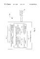
- FIG. 1is a system diagram illustrating a signal processor 100 built in accordance with the invention having a processing circuitry 140 that contains a re-configurable circuitry 105 .
- the processing circuitry 140 of the signal processor 100contains the re-configurable circuitry 105 to perform at least a portion of its total signal processing.
- the re-configurable circuitry 105contains, among other things, a programmable logic circuitry 110 , a processing power consumption analysis circuitry 120 , and a programmable logic configuration circuitry 130 .
- the programmable logic configuration circuitry 130itself contains, among other things, a default configuration circuitry 132 , an adaptive configuration circuitry 134 , an active configuration circuitry 136 , and a loading configuration circuitry (buffer) 138 .
- the programmable logic configuration circuitry 130selects a predetermined logic configuration from among a predetermined plurality of default logic configurations contained within the default configuration circuitry 132 .
- the programmable logic configuration circuitry 130programs the programmable logic circuitry 110 to perform at least one predetermined function within the signal processor 100 .
- the programmable logic configuration circuitry 130selects an alternative logic configuration using the adaptive configuration circuitry 134 .
- the adaptive configuration circuitry 134selects the alternative logic configuration in response to a number of factors including, among other things, a plurality of input data that is given to the signal processor 100 .
- the adaptive configuration circuitry 134selects the alternative logic configuration in response to the amount of power being consumed by the signal processor 100 . This determination of the amount of power being consumed is made using the processing power consumption analysis circuitry 120 . Regardless of what specific parameters are used to identify and select an appropriate logic configuration, the programmable logic configuration circuitry 130 programs the programmable logic circuitry 110 to perform the predetermined functionality of the signal processor 100 .
- the active configuration circuitry 136 of the programmable logic configuration circuitry 130is the actual configuration that is presently being employed by the signal processor 100 . That is to say, the active configuration circuitry 136 performs the actual logic configuration of the signal processor 100 during real time operation.
- the loading configuration circuitry (buffer) 138is simultaneously loading another logic configuration into the programmable logic configuration circuitry 130 while the active configuration circuitry 136 is busy configuring the programmable logic configuration circuitry 130 using either the default configuration circuitry 132 or the adaptive configuration circuitry 134 , depending on the specific application.
- the implementation of both the active configuration circuitry 136 and the loading configuration circuitry (buffer) 138is performed in a “ping-pong” style operation known to those having skill in the art of logic configuring, data management, and data processing, among other things.
- the programmable logic configuration circuitry 130employs the active configuration circuitry 136 to perform the actual logic configuration of the signal processor 100 while the loading configuration circuitry (buffer) 138 is loading a logic configuration to be used next. Then, after the present logic configuration of the programmable logic configuration circuitry 130 has been loaded by the active configuration circuitry 136 to process a first plurality of input data, the next logic configuration that was just previously contained within the loading configuration circuitry (buffer) 138 is then passed to the active configuration circuitry 136 to perform processing on a next plurality of input data.
- various logic configurationsare used to perform processing on the same plurality of input data, and in such a case, the present and the next logic configurations are used to configure the programmable logic configuration circuitry 130 at various phases within the processing of the same plurality of input data.
- the simultaneous operation of the programming of one logic configuration to the programmable logic configuration circuitry 130 using the active configuration circuitry 136 while another logic configuration is being loaded into the loading configuration circuitry (buffer) 138provides for faster, overall operation of the signal processor 100 , given that a next logic configuration is immediately ready for the programmable logic configuration circuitry 130 after the processing of the plurality of input data.
- FIG. 2is a system diagram illustrating a signal processor 200 built in accordance with the invention having a re-configurable logic circuitry 250 governed by a configuration control circuitry 210 .
- the signal processor 200operates to convert a plurality of input data 220 into a plurality of output data 240 .
- the configuration control circuitry 210operates cooperatively with a programmable logic configuration circuitry 230 to program the re-configurable logic circuitry 250 .
- the programmable logic configuration circuitry 230itself contains, among other things, a read only memory (ROM) 232 and a random access memory (RAM) 234 .
- ROMread only memory
- RAMrandom access memory
- the re-configurable logic circuitry 250itself contains, among other things, an input programmable logic circuitry 252 , a main programmable logic circuitry 254 , and an output programmable logic circuitry 256 .
- the read only memory (ROM) 232 and the random access memory (RAM) 234store a predetermined number of logic configurations that are used to program the re-configurable logic circuitry 250 . If desired, the read only memory (ROM) 232 store a predetermined number of fixed logic configurations for the re-configurable logic circuitry 250 .
- the fixed logic configurationsincludes at least one default logic configuration for the re-configurable logic circuitry 250 that is loaded during startup of the signal processor 200 or, alternatively, during any power cycle or reset operations that the signal processor 200 undergoes.
- the random access memory (RAM) 234operates within the signal processor 200 to determine amore appropriate logic configuration for the re-configurable logic circuitry 250 through adaptive techniques employed by the programmable logic configuration circuitry 230 .
- the programmable logic configuration circuitry 230analyzes various parameters to determine an appropriate logic configuration for the signal processor 200 .
- the programmable logic configuration circuitry 230provides the proper logic configuration to the re-configurable logic circuitry 250 . Irrespective of whether the programmable logic configuration circuitry 230 loads a predetermined logic configuration from the read only memory (ROM) 232 or an adaptively selected logic configuration from the random access memory (RAM) 234 , the programmable logic configuration circuitry 230 performs the programming of the re-configurable logic circuitry 250 so that the re-configurable logic circuitry 250 operates properly on the plurality of input data 220 .
- ROMread only memory
- RAMrandom access memory
- the programming of the programmable logic configuration circuitry 230operates to program the logic configuration for at least one of the input programmable logic circuitry 252 , the main programmable logic circuitry 254 , and the output programmable logic circuitry 256 .
- all of the input programmable logic circuitry 252 , the main programmable logic circuitry 254 , and the output programmable logic circuitry 256are provides with a logic configuration.
- only one of the input programmable logic circuitry 252 , the main programmable logic circuitry 254 , and the output programmable logic circuitry 256is provided with a modified logic configuration to perform processing on the plurality of input data 220 .
- the signal processor 200performs updating of new logic configurations during each passing of a clock signal's cycle of the signal processor 200 , the logic configurations of each of the input programmable logic circuitry 252 , the main programmable logic circuitry 254 , and the output programmable logic circuitry 256 is analyzed to determine if the present logic configuration is appropriate for the particular segment of the plurality of input data 220 on which the signal processor 200 is operating. If it is determined that existing logic configuration for at least one of the input programmable logic circuitry 252 , the main programmable logic circuitry 254 , and the output programmable logic circuitry 256 is appropriate for the plurality of input data 220 within the given clock signal's cycle, then that particular logic configuration is maintained.
- the logic configurations of the input programmable logic circuitry 252 , the main programmable logic circuitry 254 , and the output programmable logic circuitry 256 that need to be modifiedare indeed modified, as required and governed by the plurality of input data 220 .
- the signal processor 200then utilizes the logic configurations to generate the plurality of output data 240 .
- the various portions of the re-configurable logic circuitry 250are re-configurable to accommodate various types of the plurality of input data 220 . If desired, the signal processor 200 operates into a low power consumption mode wherein default logic configurations are loaded into each of the input programmable logic circuitry 252 , the main programmable logic circuitry 254 , and the output programmable logic circuitry 256 .
- Various intelligenceis employed in the programmable logic configuration circuitry 230 to determine, in various low power consumption modes, whether it is more power efficient to switch to a new logic configuration for at least one of the input programmable logic circuitry 252 , the main programmable logic circuitry 254 , and the output programmable logic circuitry 256 within the re-configurable logic circuitry 250 or to remain with a default logic configuration.
- those having skill in the art of data processingwill recognize that various permutations of the modification of the logic configuration of the re-configurable logic circuitry 250 is performed depending on various operational considerations of the signal processor 200 .
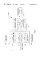
- FIG. 3is a system diagram illustrating a signal processor 300 built in accordance with the invention having a plurality of reconfigurable components.
- a programmable logic configuration circuitry 330is operable to provide configuration to each of a data memory 310 , a data addressing unit 320 , a program memory 340 , an arithmetic logic unit 350 , and an instruction decode & sequencing unit 360 ; the programmable logic configuration circuitry 330 is operable to provide updated configuration for each of the above mentioned reconfigurable components.
- the programmable logic configuration circuitry 330itself contains, among other things, a read only memory (ROM) 332 and a random access memory (RAM) 334 .
- ROMread only memory
- RAMrandom access memory
- the signal processor 300is operable using the programmable logic configuration circuitry 330 to perform both default and adaptive configuration of the various reconfigurable components contained within the signal processor 300 .
- the data memory 310itself contains, among other things, a word width 312 , an addressing logic circuitry 314 , and a random access memory (RAM) 316 .
- the data addressing unit 320itself contains, among other things, a plurality of addressing modes 322 wherein the plurality of addressing modes 322 include, among other addressing modes, an indirect addressing mode 323 , an indexed addressing mode 324 , a based offset addressing mode 325 , a first in/first out (FIFO) addressing mode 326 , and a stack addressing mode 327 .
- the program memory 340itself contains, among other things, a read only memory (ROM) 346 .
- the program memory 340provides a plurality of immediate data 370 that is stored in the program memory 340 to the arithmetic logic unit 350 , and the instruction decode & sequencing unit 360 .
- the arithmetic logic unit 350itself contains, among other things, a word width 352 and an addressing logic circuitry 354 .
- the various data addressing mode functionality of the data addressing unit 320are known to those having skill in the art of data processing. Any appropriate data addressing mode is used within the invention without departing from the scope and spirit thereof.
- the word width 312 of the data memory 310 and the word width 352 of the arithmetic logic unit 350correspond to a word width in which each of the data memory 310 and the arithmetic logic unit 350 is configured within one given updating logic configuration step.
- the programmable logic configuration circuitry 330operates to modify the logic configuration of each of the data memory 310 , the data addressing unit 320 , the program memory 340 , the arithmetic logic unit 350 , and the instruction decode & sequencing unit 360 , a wide word width that is loaded in parallel is used so that all of the configuration of the above mentioned reconfigurable components are re-configured simultaneously, if desired.
- only a subset of the data memory 310 , the data addressing unit 320 , the program memory 340 , the arithmetic logic unit 350 , and the instruction decode & sequencing unit 360is updated with a new logic configuration in any given logic configuration updating performed by the programmable logic configuration circuitry 330 of the signal processor 300 .
- the addressing logic circuitry 314 of the data memory 310 and the addressing logic circuitry 354 of the arithmetic logic unit 350operate to perform the addressing of modified and updated logic configurations within the signal processor 300 as required by various parameters including characteristics of a plurality of input data, similar to the embodiment shown above and described within the signal processor 200 of FIG. 2 .
- FIG. 4is a system diagram illustrating a signal processor 400 built in accordance with the invention that selects at least one configuration option to program a programmable logic array circuitry 440 .
- the signal processor 400contains, among other things, a memory 410 , an ‘n’ bit word width bus that performs parallel configuration loading 420 , a logic configuration selection circuitry 430 , and the programmable logic array circuitry 440 .
- the memory 410contains, among other things, a configuration option # 1 412 , a configuration option # 2 414 , and a configuration option #‘n’ 416 .
- the logic configuration selection circuitry 430that itself contains, among other things, a data monitoring circuitry 432 , provides information to the memory 410 to determine which logic configuration is appropriate for a given portion of data.
- the given portion of datais a plurality of input data, as described above in the various embodiments of the invention shown in FIGS. 2 and 3.
- the data monitoring circuitry 432is operable to identify characteristics of the plurality of input data and to provide information to the logic configuration selection circuitry 430 so that it operates to perform selection of a logic configuration that is most appropriate.
- the logic configuration selection circuitry 430cooperates with the memory 410 , selecting from among the configuration option #1 412 , the configuration option # 2 414 , and the configuration option #‘n’ 416 to identify an appropriate logic configuration for the plurality of input data.
- the selection of the appropriate logic configurationis made using various indicia in accordance with the invention. Examples of such indicia and parameters include power consumption within the signal processor 400 , the characteristics of the plurality of input data provided to the signal processor 400 , and other parameters.
- the selected logic configurationis transported to the programmable logic array circuitry 440 via the ‘n’ bit word width bus that performs parallel configuration loading 420 .
- the ‘n’ bit word width of the ‘n’ bit word width bus that performs parallel configuration loading 420provides very fast loading and configuration of the programmable logic array circuitry 440 .
- the entirety of the programmable logic array circuitry 440is programmable with a modified logic configuration within a given clock signal's cycle, i.e., all of the logic elements of the programmable logic array circuitry 440 are re-programmable in one given step.
- the programmable logic array circuitry 440itself contains, among other things, a plurality of logic elements including a logic element # 1 , 1 441 , a logic element # 1 , 2 442 , a logic element # 1 ,‘n’ 443 , a logic element # 2 , 1 444 , a logic element # 2 , 2 445 , a logic element # 2 ,‘n’ 446 , a logic element #‘n’, 1 447 , a logic element #‘n’, 2 448 , and a logic element #‘n’,‘n’ 449 .
- the width of the programmable logic array circuitry 440is ‘n’ bits that is different than the ‘n’ bit word width of the ‘n’ bit word width bus that performs parallel configuration loading 420 and only a predetermined portion of the individual logic elements of the programmable logic array circuitry 440 is programmed with a modified logic configuration in the given clock signal's cycle. Additional clock signal cycles are required to modify the logic configuration of the remainder of the programmable logic array circuitry 440 .
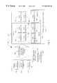
- FIG. 5is a system diagram illustrating a signal processor 500 built in accordance with the invention that selects at least one area configuration to program at least one area of a programmable logic array circuitry.
- the signal processor 500contains, among other things, a memory 510 , an ‘n’ bit word width bus that performs parallel configuration loading 520 , a logic configuration selection circuitry 530 , and a programmable logic array circuitry 540 .
- the memory 510contains, among other things, a configuration option #1 512 , a configuration option # 2 514 , and a configuration option #‘n’ 516 .
- the logic configuration selection circuitry 530that itself contains, among other things, a data monitoring circuitry 532 , provides information to the memory 510 to determine which logic configuration is appropriate for a given portion of data. Similar to the embodiment of the invention described above in the signal processor 400 of FIG. 4, the given portion of data is a plurality of input data, as described above in the various embodiments of the invention shown in FIGS. 2 and 3.
- the data monitoring circuitry 532is operable to identify characteristics of the plurality of input data and to provide information to the logic configuration selection circuitry 530 so that it operates to perform selection of a logic configuration that is most appropriate.
- the logic configuration selection circuitry 530cooperates with the memory 510 , selecting from among the configuration option #1 512 , the configuration option #2 514 , and the configuration option #‘n’ 516 to identify an appropriate logic configuration for the plurality of input data.
- the selection of the appropriate logic configurationis made using various indicia in accordance with the invention. Examples of such indicia and parameters include power consumption within the signal processor 500 , the characteristics of the plurality of input data provided to the signal processor 500 , and other parameters.
- the selected logic configurationis transported to the programmable logic array circuitry 540 via the ‘n’ bit word width bus that performs parallel configuration loading 520 .
- the ‘n’ bit word width of the ‘n’ bit word width bus that performs parallel configuration loading 520provides very fast loading and configuration of the programmable logic array circuitry 540 .
- the entirety of the programmable logic array circuitry 540is programmable with a modified logic configuration within a given clock signal's cycle, i.e., all of the logic elements of the programmable logic array circuitry 540 are re-programmable in one given step.
- the programmable logic array circuitry 540itself contains, among other things, a plurality of logic elements including a logic element # 1 , 1 541 , a logic element # 1 , 2 542 , a logic element #1,‘n’ 543 , a logic element #2, 1 544 , a logic element #2, 2 545 , a logic element #2,‘n’ 546 , a logic element #‘n’, 1 547 , a logic element #‘n’, 2 548 , and a logic element #‘n’,‘n’ 549 .
- the programmable logic array circuitry 540is not only partitioned into the logic element # 1 , 1 541 , the logic element # 1 , 2 542 , the logic element # 1 ,‘n’ 543 , the logic element # 2 , 1 544 , the logic element # 2 , 2 545 , the logic element #2,‘n’ 546 , the logic element #‘n’,1 547 , the logic element #‘n’,2 548 , and the logic element #‘n’,‘n’ 549 , but the programmable logic array circuitry 540 is further organized into an area #1 552 , an area# 2 554 , and an area #‘n’ 556 .
- the area # 1 552contains the logic element #1, 1 541 , the logic element # 1 , 2 542 , the logic element # 2 , 1 544 , and the logic element # 2 , 2 545 ;
- the area # 2 554contains the logic element #‘n’, 1 547 and the logic element #‘n’, 2 548 ;
- the area #‘n’ 556contains the logic element #‘n’,‘n’ 549 .
- the signal processor 500is operable to provide various logic configurations to each of the area # 1 552 , the area # 2 554 , and the area #‘n’ 556 as required by the specific application.
- the the logic element # 1 , 1 541 , the logic element # 1 , 2 542 , the logic element # 1 ,‘n’ 543 , the logic element # 2 , 1 544 , the logic element # 2 , 2 545 , the logic element # 2 ,‘n’ 546 , the logic element #‘n’, 1 547 , the logic element #‘n’, 2 548 , and the logic element #‘n’,‘n’ 549is operable to be organized into any number of individual areas such that predetermined logic configurations are loaded into the various areas of the programmable logic array circuitry 540 for processing within the signal processor 500 .
- FIG. 6is a system diagram illustrating a signal processor 600 built in accordance with the invention that performs recursive updating of a programmable logic configuration circuitry 630 and a programmable logic array circuitry 640 .
- the signal processor 600contains, among other things, a logic configuration selection circuitry 650 that is coupled to a programmable logic configuration circuitry 630 and a programmable logic array circuitry 640 .
- the programmable logic configuration circuitry 630 and the programmable logic array circuitry 640are additionally coupled to one another via an ‘n’ bit word width bus that performs parallel configuration loading 620 .
- the logic configuration selection circuitry 650selects from the programmable logic configuration circuitry 630 a logic configuration that is appropriate for the signal processor 600 .
- the signal processor 600utilized information of the existing logic configuration programmed in the programmable logic array circuitry 640 .
- the selection of an appropriate logic configurationselected from the programmable logic configuration circuitry 630 , and the updating of the selected logic configuration into the programmable logic array circuitry 640 are each performed using a recursive updating circuitry 690 and a recursive updating circuitry 692 , respectively. That is to say, adaptive logic configuration is supportable within the programmable logic configuration circuitry 630 using the recursive updating circuitry 690 as required by the specific application of the signal processor 600 .
- a “new” logic configurationis achieved within the programmable logic configuration circuitry 630 , even if it is not originally loaded into the programmable logic configuration circuitry 630 at the inception of the operation of the signal processor 600 . That is to say, the “new” logic configuration is generated in real time operation of the signal processor 600 to accommodate an immediate logic configuration within the programmable logic array circuitry 640 .
- the “new” logic configurationis adaptively generated specifically for the plurality of input data that is fed into the signal processor 600 . As required by a number of parameters including a plurality of input data, the power consumption of the signal processor 600 , or other parameters, the “new” logic configuration of the signal processor 600 is appropriately chosen for the present application.
- the recursive updating circuitry 690 and the recursive updating circuitry 692operate cooperatively to perform recursive updating of the programmable logic configuration circuitry 630 and the programmable logic array circuitry 640 .
- the recursive updating circuitry 690 and the recursive updating circuitry 692operate independently to perform recursive updating of the programmable logic configuration circuitry 630 and the programmable logic array circuitry 640 based upon various parameters including, among other things, the type of incoming data on which the signal processor 600 will operate and a most efficient logic array configuration that is identified by the logic configuration selection circuitry 650 .
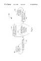
- FIG. 7is a functional block diagram illustrating a method 700 performed in accordance with the invention that reconfigures a logic array circuitry.
- a default logic configurationis selected from among a plurality of predetermined logic configurations.
- a logic array circuitryis programmed using the default logic configuration that is selected in the block 710 .
- a plurality of input datain analyzed to determine if the default logic configuration that is selected in the block 710 is appropriate.
- a power consumption of a signal processoris analyzed to perform the determination whether the default logic configuration that is selected in the block 710 is appropriate.
- an alternative logic configurationis selected in a block 740 .
- the already selected default logic configuration selected in the block 710is appropriate.
- the alternative logic configurationneed not be selected in the block 740 .
- an alternative logic configurationis selected in the block 740 that is more appropriately geared for the plurality of input data that is analyzed in the block 730 or more appropriately geared for the power consumption that is analyzed in the block 735 .
- the logic array circuitryis re-programmed using the alternative logic configuration that is selected in the block 740 .
Landscapes
- Engineering & Computer Science (AREA)
- Computer Hardware Design (AREA)
- Theoretical Computer Science (AREA)
- Physics & Mathematics (AREA)
- General Engineering & Computer Science (AREA)
- General Physics & Mathematics (AREA)
- Logic Circuits (AREA)
Abstract
Description
Claims (19)
Priority Applications (5)
| Application Number | Priority Date | Filing Date | Title |
|---|---|---|---|
| US09/408,825US6662302B1 (en) | 1999-09-29 | 1999-09-29 | Method and apparatus of selecting one of a plurality of predetermined configurations using only necessary bus widths based on power consumption analysis for programmable logic device |
| PCT/US2000/026308WO2001024030A2 (en) | 1999-09-29 | 2000-09-25 | Signal processor with fast field reconfigurable datapath, data address unit, and program sequencer |
| AU77137/00AAU7713700A (en) | 1999-09-29 | 2000-09-25 | Signal processor with fast field reconfigurable datapath, data address unit, andprogram sequencer |
| US10/686,940US20040139311A1 (en) | 1999-09-29 | 2003-10-15 | Signal processor with fast field reconfigurable datapath, data address unit, and program sequencer |
| US10/892,537US20050066152A1 (en) | 1999-09-29 | 2004-07-14 | Method and apparatus for processing data in a reconfigurable manner |
Applications Claiming Priority (1)
| Application Number | Priority Date | Filing Date | Title |
|---|---|---|---|
| US09/408,825US6662302B1 (en) | 1999-09-29 | 1999-09-29 | Method and apparatus of selecting one of a plurality of predetermined configurations using only necessary bus widths based on power consumption analysis for programmable logic device |
Related Child Applications (2)
| Application Number | Title | Priority Date | Filing Date |
|---|---|---|---|
| US10/686,940ContinuationUS20040139311A1 (en) | 1999-09-29 | 2003-10-15 | Signal processor with fast field reconfigurable datapath, data address unit, and program sequencer |
| US10/892,537ContinuationUS20050066152A1 (en) | 1999-09-29 | 2004-07-14 | Method and apparatus for processing data in a reconfigurable manner |
Publications (1)
| Publication Number | Publication Date |
|---|---|
| US6662302B1true US6662302B1 (en) | 2003-12-09 |
Family
ID=23617925
Family Applications (3)
| Application Number | Title | Priority Date | Filing Date |
|---|---|---|---|
| US09/408,825Expired - LifetimeUS6662302B1 (en) | 1999-09-29 | 1999-09-29 | Method and apparatus of selecting one of a plurality of predetermined configurations using only necessary bus widths based on power consumption analysis for programmable logic device |
| US10/686,940AbandonedUS20040139311A1 (en) | 1999-09-29 | 2003-10-15 | Signal processor with fast field reconfigurable datapath, data address unit, and program sequencer |
| US10/892,537AbandonedUS20050066152A1 (en) | 1999-09-29 | 2004-07-14 | Method and apparatus for processing data in a reconfigurable manner |
Family Applications After (2)
| Application Number | Title | Priority Date | Filing Date |
|---|---|---|---|
| US10/686,940AbandonedUS20040139311A1 (en) | 1999-09-29 | 2003-10-15 | Signal processor with fast field reconfigurable datapath, data address unit, and program sequencer |
| US10/892,537AbandonedUS20050066152A1 (en) | 1999-09-29 | 2004-07-14 | Method and apparatus for processing data in a reconfigurable manner |
Country Status (3)
| Country | Link |
|---|---|
| US (3) | US6662302B1 (en) |
| AU (1) | AU7713700A (en) |
| WO (1) | WO2001024030A2 (en) |
Cited By (20)
| Publication number | Priority date | Publication date | Assignee | Title |
|---|---|---|---|---|
| US20020108009A1 (en)* | 2000-12-29 | 2002-08-08 | Michele Borgatti | Electronic system having modular expansion function facilities |
| US20030033374A1 (en)* | 2001-07-24 | 2003-02-13 | Condor Engineering, Inc. | Method and system for implementing a communications core on a single programmable device |
| US20030056091A1 (en)* | 2001-09-14 | 2003-03-20 | Greenberg Craig B. | Method of scheduling in a reconfigurable hardware architecture with multiple hardware configurations |
| US20030154466A1 (en)* | 2002-02-11 | 2003-08-14 | Snider Gregory S. | Method and apparatus for compiling source code to configure hardware |
| US20040111231A1 (en)* | 2002-04-24 | 2004-06-10 | Yoshiyuki Ando | Integrated circuits having post-silicon adjustment control |
| US20050262284A1 (en)* | 2004-05-21 | 2005-11-24 | Naveen Cherukuri | Method for identifying bad lanes and exchanging width capabilities of two CSI agents connected across a link |
| US20060020774A1 (en)* | 2004-07-23 | 2006-01-26 | Honeywill International Inc. | Reconfigurable computing architecture for space applications |
| US20070045475A1 (en)* | 2005-08-29 | 2007-03-01 | Honeywell International Inc. | Systems and methods for semi-permanent, non-precision inspace assembly of space structures, modules and spacecraft |
| US20070046781A1 (en)* | 2005-08-29 | 2007-03-01 | Honeywell International Inc. | Systems and methods for processing digital video data |
| US20070075736A1 (en)* | 2005-09-30 | 2007-04-05 | Goodnow Kenneth J | FPGA powerup to known functional state |
| US20070075733A1 (en)* | 2005-09-30 | 2007-04-05 | International Business Machines Corporation | Fpga powerup to known functional state |
| US20070150718A1 (en)* | 2005-12-28 | 2007-06-28 | Nec Corporation | Information processing apparatus and method for using reconfigurable device |
| US20070157009A1 (en)* | 2006-01-03 | 2007-07-05 | Samsung Electronics Co., Ltd. | Loop accelerator and data processing system having the same |
| US20080022081A1 (en)* | 2006-07-18 | 2008-01-24 | Honeywell International Inc. | Local controller for reconfigurable processing elements |
| US7353474B1 (en)* | 2006-04-18 | 2008-04-01 | Xilinx, Inc. | System and method for accessing signals of a user design in a programmable logic device |
| US20090024839A1 (en)* | 2007-07-21 | 2009-01-22 | Arssov Paul Plamen | Variable instruction set microprocessor |
| US20090138696A1 (en)* | 2004-03-08 | 2009-05-28 | Altera Corporation | Systems and methods for reducing static and total power consumption |
| US20120185719A1 (en)* | 2011-01-13 | 2012-07-19 | Xilinx, Inc.. | Power management within an integrated circuit |
| US8667192B2 (en) | 2011-02-28 | 2014-03-04 | Xilinx, Inc. | Integrated circuit with programmable circuitry and an embedded processor system |
| US9401718B1 (en) | 2013-01-04 | 2016-07-26 | Altera Corporation | Heterogeneous programmable device and configuration software adapted therefor |
Families Citing this family (30)
| Publication number | Priority date | Publication date | Assignee | Title |
|---|---|---|---|---|
| US20010049757A1 (en) | 2000-03-01 | 2001-12-06 | Ming-Kang Liu | Programmable task scheduler for use with multiport xDSL processing system |
| US8149048B1 (en) | 2000-10-26 | 2012-04-03 | Cypress Semiconductor Corporation | Apparatus and method for programmable power management in a programmable analog circuit block |
| US8160864B1 (en) | 2000-10-26 | 2012-04-17 | Cypress Semiconductor Corporation | In-circuit emulator and pod synchronized boot |
| US8176296B2 (en) | 2000-10-26 | 2012-05-08 | Cypress Semiconductor Corporation | Programmable microcontroller architecture |
| US6724220B1 (en) | 2000-10-26 | 2004-04-20 | Cyress Semiconductor Corporation | Programmable microcontroller architecture (mixed analog/digital) |
| US8103496B1 (en) | 2000-10-26 | 2012-01-24 | Cypress Semicondutor Corporation | Breakpoint control in an in-circuit emulation system |
| US7406674B1 (en) | 2001-10-24 | 2008-07-29 | Cypress Semiconductor Corporation | Method and apparatus for generating microcontroller configuration information |
| US8078970B1 (en) | 2001-11-09 | 2011-12-13 | Cypress Semiconductor Corporation | Graphical user interface with user-selectable list-box |
| US8042093B1 (en) | 2001-11-15 | 2011-10-18 | Cypress Semiconductor Corporation | System providing automatic source code generation for personalization and parameterization of user modules |
| US7844437B1 (en)* | 2001-11-19 | 2010-11-30 | Cypress Semiconductor Corporation | System and method for performing next placements and pruning of disallowed placements for programming an integrated circuit |
| US6971004B1 (en) | 2001-11-19 | 2005-11-29 | Cypress Semiconductor Corp. | System and method of dynamically reconfiguring a programmable integrated circuit |
| US8069405B1 (en) | 2001-11-19 | 2011-11-29 | Cypress Semiconductor Corporation | User interface for efficiently browsing an electronic document using data-driven tabs |
| US8103497B1 (en) | 2002-03-28 | 2012-01-24 | Cypress Semiconductor Corporation | External interface for event architecture |
| FR2838208B1 (en)* | 2002-04-03 | 2005-03-11 | Centre Nat Rech Scient | LOGICAL CALCULATION ARCHITECTURE COMPRISING MULTIPLE CONFIGURATION MODES |
| US7295049B1 (en) | 2004-03-25 | 2007-11-13 | Cypress Semiconductor Corporation | Method and circuit for rapid alignment of signals |
| JP4095576B2 (en)* | 2004-05-17 | 2008-06-04 | 株式会社東芝 | General-purpose logic circuit device using programmable logic circuit |
| US7332976B1 (en)* | 2005-02-04 | 2008-02-19 | Cypress Semiconductor Corporation | Poly-phase frequency synthesis oscillator |
| US7400183B1 (en) | 2005-05-05 | 2008-07-15 | Cypress Semiconductor Corporation | Voltage controlled oscillator delay cell and method |
| US8067948B2 (en)* | 2006-03-27 | 2011-11-29 | Cypress Semiconductor Corporation | Input/output multiplexer bus |
| US8026739B2 (en) | 2007-04-17 | 2011-09-27 | Cypress Semiconductor Corporation | System level interconnect with programmable switching |
| US8040266B2 (en)* | 2007-04-17 | 2011-10-18 | Cypress Semiconductor Corporation | Programmable sigma-delta analog-to-digital converter |
| US9564902B2 (en)* | 2007-04-17 | 2017-02-07 | Cypress Semiconductor Corporation | Dynamically configurable and re-configurable data path |
| US7737724B2 (en) | 2007-04-17 | 2010-06-15 | Cypress Semiconductor Corporation | Universal digital block interconnection and channel routing |
| US8516025B2 (en)* | 2007-04-17 | 2013-08-20 | Cypress Semiconductor Corporation | Clock driven dynamic datapath chaining |
| US8130025B2 (en) | 2007-04-17 | 2012-03-06 | Cypress Semiconductor Corporation | Numerical band gap |
| US9720805B1 (en) | 2007-04-25 | 2017-08-01 | Cypress Semiconductor Corporation | System and method for controlling a target device |
| US8049569B1 (en) | 2007-09-05 | 2011-11-01 | Cypress Semiconductor Corporation | Circuit and method for improving the accuracy of a crystal-less oscillator having dual-frequency modes |
| US7752592B2 (en)* | 2007-10-10 | 2010-07-06 | International Business Machines Corporation | Scheduler design to optimize system performance using configurable acceleration engines |
| JP5332598B2 (en)* | 2008-12-25 | 2013-11-06 | 富士通セミコンダクター株式会社 | Design method and design apparatus |
| GB201414286D0 (en) | 2014-08-12 | 2014-09-24 | Imp Innovations Ltd | Reconfigurable integrated circuit with on-chip configuration generation |
Citations (18)
| Publication number | Priority date | Publication date | Assignee | Title |
|---|---|---|---|---|
| JPH04282475A (en)* | 1991-03-11 | 1992-10-07 | Kawasaki Steel Corp | programmable logic device |
| US5497498A (en) | 1992-11-05 | 1996-03-05 | Giga Operations Corporation | Video processing module using a second programmable logic device which reconfigures a first programmable logic device for data transformation |
| US5535406A (en)* | 1993-12-29 | 1996-07-09 | Kolchinsky; Alexander | Virtual processor module including a reconfigurable programmable matrix |
| US5537295A (en) | 1994-03-04 | 1996-07-16 | Altera Corporation | Universal reconfigurable printed circuit board |
| US5737631A (en)* | 1995-04-05 | 1998-04-07 | Xilinx Inc | Reprogrammable instruction set accelerator |
| US5751164A (en)* | 1996-06-24 | 1998-05-12 | Advanced Micro Devices, Inc. | Programmable logic device with multi-level power control |
| US5841810A (en)* | 1997-01-30 | 1998-11-24 | National Semiconductor Corporation | Multiple stage adaptive equalizer |
| US5887165A (en)* | 1996-06-21 | 1999-03-23 | Mirage Technologies, Inc. | Dynamically reconfigurable hardware system for real-time control of processes |
| US5931959A (en)* | 1997-05-21 | 1999-08-03 | The United States Of America As Represented By The Secretary Of The Air Force | Dynamically reconfigurable FPGA apparatus and method for multiprocessing and fault tolerance |
| US5933642A (en)* | 1995-04-17 | 1999-08-03 | Ricoh Corporation | Compiling system and method for reconfigurable computing |
| US5956518A (en)* | 1996-04-11 | 1999-09-21 | Massachusetts Institute Of Technology | Intermediate-grain reconfigurable processing device |
| US5996083A (en)* | 1995-08-11 | 1999-11-30 | Hewlett-Packard Company | Microprocessor having software controllable power consumption |
| US6134707A (en)* | 1996-11-14 | 2000-10-17 | Altera Corporation | Apparatus and method for in-system programming of integrated circuits containing programmable elements |
| US6172518B1 (en)* | 1999-07-23 | 2001-01-09 | Xilinx, Inc. | Method of minimizing power use in programmable logic devices |
| US6175434B1 (en)* | 1996-12-23 | 2001-01-16 | International Business Machines Corporation | Adaptive infrared communication apparatus |
| US6198304B1 (en)* | 1998-02-23 | 2001-03-06 | Xilinx, Inc. | Programmable logic device |
| US6314551B1 (en)* | 1998-06-22 | 2001-11-06 | Morgan Stanley & Co. Incorporated | System processing unit extended with programmable logic for plurality of functions |
| US6421728B1 (en)* | 1997-12-31 | 2002-07-16 | Intel Corporation | Architecture for communicating with and controlling separate upstream and downstream devices |
Family Cites Families (10)
| Publication number | Priority date | Publication date | Assignee | Title |
|---|---|---|---|---|
| US5301344A (en)* | 1991-01-29 | 1994-04-05 | Analogic Corporation | Multibus sequential processor to perform in parallel a plurality of reconfigurable logic operations on a plurality of data sets |
| US5426378A (en)* | 1994-04-20 | 1995-06-20 | Xilinx, Inc. | Programmable logic device which stores more than one configuration and means for switching configurations |
| US5600845A (en)* | 1994-07-27 | 1997-02-04 | Metalithic Systems Incorporated | Integrated circuit computing device comprising a dynamically configurable gate array having a microprocessor and reconfigurable instruction execution means and method therefor |
| US5794062A (en)* | 1995-04-17 | 1998-08-11 | Ricoh Company Ltd. | System and method for dynamically reconfigurable computing using a processing unit having changeable internal hardware organization |
| US5933023A (en)* | 1996-09-03 | 1999-08-03 | Xilinx, Inc. | FPGA architecture having RAM blocks with programmable word length and width and dedicated address and data lines |
| US5970254A (en)* | 1997-06-27 | 1999-10-19 | Cooke; Laurence H. | Integrated processor and programmable data path chip for reconfigurable computing |
| US5915123A (en)* | 1997-10-31 | 1999-06-22 | Silicon Spice | Method and apparatus for controlling configuration memory contexts of processing elements in a network of multiple context processing elements |
| US6028445A (en)* | 1997-12-30 | 2000-02-22 | Xilinx, Inc. | Decoder structure and method for FPGA configuration |
| US6094726A (en)* | 1998-02-05 | 2000-07-25 | George S. Sheng | Digital signal processor using a reconfigurable array of macrocells |
| US6145020A (en)* | 1998-05-14 | 2000-11-07 | Advanced Technology Materials, Inc. | Microcontroller incorporating an enhanced peripheral controller for automatic updating the configuration date of multiple peripherals by using a ferroelectric memory array |
- 1999
- 1999-09-29USUS09/408,825patent/US6662302B1/ennot_activeExpired - Lifetime
- 2000
- 2000-09-25AUAU77137/00Apatent/AU7713700A/ennot_activeAbandoned
- 2000-09-25WOPCT/US2000/026308patent/WO2001024030A2/enactiveApplication Filing
- 2003
- 2003-10-15USUS10/686,940patent/US20040139311A1/ennot_activeAbandoned
- 2004
- 2004-07-14USUS10/892,537patent/US20050066152A1/ennot_activeAbandoned
Patent Citations (18)
| Publication number | Priority date | Publication date | Assignee | Title |
|---|---|---|---|---|
| JPH04282475A (en)* | 1991-03-11 | 1992-10-07 | Kawasaki Steel Corp | programmable logic device |
| US5497498A (en) | 1992-11-05 | 1996-03-05 | Giga Operations Corporation | Video processing module using a second programmable logic device which reconfigures a first programmable logic device for data transformation |
| US5535406A (en)* | 1993-12-29 | 1996-07-09 | Kolchinsky; Alexander | Virtual processor module including a reconfigurable programmable matrix |
| US5537295A (en) | 1994-03-04 | 1996-07-16 | Altera Corporation | Universal reconfigurable printed circuit board |
| US5737631A (en)* | 1995-04-05 | 1998-04-07 | Xilinx Inc | Reprogrammable instruction set accelerator |
| US5933642A (en)* | 1995-04-17 | 1999-08-03 | Ricoh Corporation | Compiling system and method for reconfigurable computing |
| US5996083A (en)* | 1995-08-11 | 1999-11-30 | Hewlett-Packard Company | Microprocessor having software controllable power consumption |
| US5956518A (en)* | 1996-04-11 | 1999-09-21 | Massachusetts Institute Of Technology | Intermediate-grain reconfigurable processing device |
| US5887165A (en)* | 1996-06-21 | 1999-03-23 | Mirage Technologies, Inc. | Dynamically reconfigurable hardware system for real-time control of processes |
| US5751164A (en)* | 1996-06-24 | 1998-05-12 | Advanced Micro Devices, Inc. | Programmable logic device with multi-level power control |
| US6134707A (en)* | 1996-11-14 | 2000-10-17 | Altera Corporation | Apparatus and method for in-system programming of integrated circuits containing programmable elements |
| US6175434B1 (en)* | 1996-12-23 | 2001-01-16 | International Business Machines Corporation | Adaptive infrared communication apparatus |
| US5841810A (en)* | 1997-01-30 | 1998-11-24 | National Semiconductor Corporation | Multiple stage adaptive equalizer |
| US5931959A (en)* | 1997-05-21 | 1999-08-03 | The United States Of America As Represented By The Secretary Of The Air Force | Dynamically reconfigurable FPGA apparatus and method for multiprocessing and fault tolerance |
| US6421728B1 (en)* | 1997-12-31 | 2002-07-16 | Intel Corporation | Architecture for communicating with and controlling separate upstream and downstream devices |
| US6198304B1 (en)* | 1998-02-23 | 2001-03-06 | Xilinx, Inc. | Programmable logic device |
| US6314551B1 (en)* | 1998-06-22 | 2001-11-06 | Morgan Stanley & Co. Incorporated | System processing unit extended with programmable logic for plurality of functions |
| US6172518B1 (en)* | 1999-07-23 | 2001-01-09 | Xilinx, Inc. | Method of minimizing power use in programmable logic devices |
Non-Patent Citations (13)
| Title |
|---|
| Andre DeHon, "DPGA-Coupled Microprocessors: Commodity IC's for the Early 21<st >Century," Mit Transit Note #100, Jan. 1994 (12 pages). |
| Andre DeHon, "DPGA-Coupled Microprocessors: Commodity IC's for the Early 21st Century," Mit Transit Note #100, Jan. 1994 (12 pages). |
| Bradley K. Fawcett, "FPGAs in Reconfigurable Computing Applications," pp. 261-266. |
| D.M. Budgett, P.E. Tang, J.H. Sharp, C.R. Chatwin, R.C.D. Young, R.K. Wang and B.F. Scott, "Parallel Pixel Processing using Programmable Gate Arrays," IEEE 1996, Electronic Letters Online, No. 19961025, Jun. 1996 (2 pages). |
| David M. James, "Reconfigurable Pipeline for Fast, Versatile Computation," IEEE, 1998, pp. 1710-1713. |
| Edward A. Acosta, V. Michael Bove, Jr., John A Watlington, and Ross A Yu, "Reconfigurable Processor for Data-Flow Video Processing System," SPIE, vol. 2607, 1995, pp. 83-89. |
| Endler, M.; Wei, J.; "Programming generic dynamic reconfigurations for distributed applications", Configurable Distributed Systems, 1992., International Workshop on, Mar. 25-27, 1992, Page(s): 68-79.** |
| Ian Page, "Reconfigurable Processor Architectures," Elsevier: Microprocessors and Microsystems, vol. 20, 1996, pp. 185-196. |
| Phil Lapsley and Garrick Blalock, "How to Estimate DSP Performance," IEEE Spectrum, Jul. 1996, pp. 74-78. |
| Ray Bittner and Peter Athanes, "Wormhole Run-time Reconfiguration," (8 pages). |
| Stan baker, " Programming Silicon: Dynamic Reinvention," Electronic Engineering Times, Aug. 28, 1995, p. 73. |
| Tannenbaum, Andrew S., Structured Computer Organization, 1984, Prentice-Hall, pp. 10-12.** |
| W.D. Zhong, S. Dods, J.P.R. Lacey and R.S. Tucker, "Reconfigurable Multichannel Add-drop Multiplexer with Improved Performance," IEE 1996, Electronics Letters Online, No. 19960989, May 1996, (2 pages). |
Cited By (37)
| Publication number | Priority date | Publication date | Assignee | Title |
|---|---|---|---|---|
| US20020108009A1 (en)* | 2000-12-29 | 2002-08-08 | Michele Borgatti | Electronic system having modular expansion function facilities |
| US7350008B2 (en) | 2000-12-29 | 2008-03-25 | Stmicroelectronics S.R.L. | Electronic system having modular expansion function facilities |
| US20070067536A1 (en)* | 2000-12-29 | 2007-03-22 | Michele Borgatti | Electronic system having modular expansion function facilities |
| US20030033374A1 (en)* | 2001-07-24 | 2003-02-13 | Condor Engineering, Inc. | Method and system for implementing a communications core on a single programmable device |
| US20030056091A1 (en)* | 2001-09-14 | 2003-03-20 | Greenberg Craig B. | Method of scheduling in a reconfigurable hardware architecture with multiple hardware configurations |
| US20030154466A1 (en)* | 2002-02-11 | 2003-08-14 | Snider Gregory S. | Method and apparatus for compiling source code to configure hardware |
| US6988192B2 (en)* | 2002-02-11 | 2006-01-17 | Hewlett-Packard Development Company, L.P. | Method and apparatus for compiling source code to configure hardware |
| US6957163B2 (en)* | 2002-04-24 | 2005-10-18 | Yoshiyuki Ando | Integrated circuits having post-silicon adjustment control |
| US20040111231A1 (en)* | 2002-04-24 | 2004-06-10 | Yoshiyuki Ando | Integrated circuits having post-silicon adjustment control |
| US8156355B2 (en)* | 2004-03-08 | 2012-04-10 | Altera Corporation | Systems and methods for reducing static and total power consumption |
| US20090138696A1 (en)* | 2004-03-08 | 2009-05-28 | Altera Corporation | Systems and methods for reducing static and total power consumption |
| US20050262284A1 (en)* | 2004-05-21 | 2005-11-24 | Naveen Cherukuri | Method for identifying bad lanes and exchanging width capabilities of two CSI agents connected across a link |
| US7844767B2 (en)* | 2004-05-21 | 2010-11-30 | Intel Corporation | Method for identifying bad lanes and exchanging width capabilities of two CSI agents connected across a link |
| US20060020774A1 (en)* | 2004-07-23 | 2006-01-26 | Honeywill International Inc. | Reconfigurable computing architecture for space applications |
| US7320064B2 (en)* | 2004-07-23 | 2008-01-15 | Honeywell International Inc. | Reconfigurable computing architecture for space applications |
| US20070045475A1 (en)* | 2005-08-29 | 2007-03-01 | Honeywell International Inc. | Systems and methods for semi-permanent, non-precision inspace assembly of space structures, modules and spacecraft |
| US7374134B2 (en) | 2005-08-29 | 2008-05-20 | Honeywell International Inc. | Systems and methods for semi-permanent, non-precision inspace assembly of space structures, modules and spacecraft |
| US20070046781A1 (en)* | 2005-08-29 | 2007-03-01 | Honeywell International Inc. | Systems and methods for processing digital video data |
| US20080030226A1 (en)* | 2005-09-30 | 2008-02-07 | Goodnow Kenneth J | Fpga powerup to known functional state |
| US7282949B2 (en) | 2005-09-30 | 2007-10-16 | International Business Machines Corporation | FPGA powerup to known functional state |
| US20070075736A1 (en)* | 2005-09-30 | 2007-04-05 | Goodnow Kenneth J | FPGA powerup to known functional state |
| US20070075733A1 (en)* | 2005-09-30 | 2007-04-05 | International Business Machines Corporation | Fpga powerup to known functional state |
| US7489163B2 (en) | 2005-09-30 | 2009-02-10 | International Business Machines Corporation | FPGA powerup to known functional state |
| US7304493B2 (en) | 2005-09-30 | 2007-12-04 | International Business Machines Corporation | FPGA powerup to known functional state |
| US20070150718A1 (en)* | 2005-12-28 | 2007-06-28 | Nec Corporation | Information processing apparatus and method for using reconfigurable device |
| JP2007179358A (en)* | 2005-12-28 | 2007-07-12 | Nec Corp | Information processor and method of using reconfiguration device |
| US7793092B2 (en)* | 2005-12-28 | 2010-09-07 | Nec Corporation | Information processing apparatus and method for using reconfigurable device |
| US20070157009A1 (en)* | 2006-01-03 | 2007-07-05 | Samsung Electronics Co., Ltd. | Loop accelerator and data processing system having the same |
| US7590831B2 (en)* | 2006-01-03 | 2009-09-15 | Samsung Electronics Co., Ltd. | Loop accelerator and data processing system having the same |
| US7353474B1 (en)* | 2006-04-18 | 2008-04-01 | Xilinx, Inc. | System and method for accessing signals of a user design in a programmable logic device |
| US20080022081A1 (en)* | 2006-07-18 | 2008-01-24 | Honeywell International Inc. | Local controller for reconfigurable processing elements |
| US20090024839A1 (en)* | 2007-07-21 | 2009-01-22 | Arssov Paul Plamen | Variable instruction set microprocessor |
| US20120185719A1 (en)* | 2011-01-13 | 2012-07-19 | Xilinx, Inc.. | Power management within an integrated circuit |
| US8612789B2 (en)* | 2011-01-13 | 2013-12-17 | Xilinx, Inc. | Power management within an integrated circuit |
| US8667192B2 (en) | 2011-02-28 | 2014-03-04 | Xilinx, Inc. | Integrated circuit with programmable circuitry and an embedded processor system |
| US9454498B1 (en) | 2011-02-28 | 2016-09-27 | Xilinx, Inc. | Integrated circuit with programmable circuitry and an embedded processor system |
| US9401718B1 (en) | 2013-01-04 | 2016-07-26 | Altera Corporation | Heterogeneous programmable device and configuration software adapted therefor |
Also Published As
| Publication number | Publication date |
|---|---|
| WO2001024030A3 (en) | 2002-03-28 |
| WO2001024030A2 (en) | 2001-04-05 |
| US20050066152A1 (en) | 2005-03-24 |
| AU7713700A (en) | 2001-04-30 |
| US20040139311A1 (en) | 2004-07-15 |
Similar Documents
| Publication | Publication Date | Title |
|---|---|---|
| US6662302B1 (en) | Method and apparatus of selecting one of a plurality of predetermined configurations using only necessary bus widths based on power consumption analysis for programmable logic device | |
| US6961841B2 (en) | Multiprocessor computer architecture incorporating a plurality of memory algorithm processors in the memory subsystem | |
| US6023564A (en) | Data processing system using a flash reconfigurable logic device as a dynamic execution unit for a sequence of instructions | |
| US6803787B1 (en) | State machine in a programmable logic device | |
| US4984151A (en) | Flexible, next-address generation microprogram sequencer | |
| US20020133688A1 (en) | SIMD/MIMD processing on a reconfigurable array | |
| US5412785A (en) | Microprogrammed data processor which includes a microsequencer in which a next microaddress output of a microROM is connected to the or-plane of an entry PLA | |
| US5276824A (en) | Data processor having a multi-stage instruction pipe and selection logic responsive to an instruction decoder for selecting one stage of the instruction pipe | |
| KR20000076310A (en) | Eight-bit microcontroller having a risc architecture | |
| EP0942359B1 (en) | An apparatus for executing instructions of a program | |
| US4115852A (en) | Microprogrammed controller | |
| US20070271440A1 (en) | Computer processor architecture selectively using finite-state-machine for control code execution | |
| US5241637A (en) | Data processor microsequencer having multiple microaddress sources and next microaddress source selection | |
| US7831807B1 (en) | System and method for expanding the instruction set of an instruction processor | |
| US4972342A (en) | Programmable priority branch circuit | |
| US7290157B2 (en) | Configurable processor with main controller to increase activity of at least one of a plurality of processing units having local program counters | |
| US5124910A (en) | Microprogram control apparatus for generating a branch condition signal to be designated by a micro-branch instruction | |
| US20040236929A1 (en) | Logic circuit and program for executing thereon | |
| US6099585A (en) | System and method for streamlined execution of instructions | |
| EP1927056A2 (en) | Processor array with separate serial module | |
| JPH1091430A (en) | Command decoding device | |
| US20020133687A1 (en) | Facilitating automatic incrementing and/or decrementing of data pointers in a microcontroller | |
| US6038659A (en) | Method for using read-only memory to generate controls for microprocessor | |
| JPH0876996A (en) | Programmable controller | |
| JP2804266B2 (en) | Entry point mapping and skipping method and apparatus |
Legal Events
| Date | Code | Title | Description |
|---|---|---|---|
| AS | Assignment | Owner name:CONEXANT SYSTEMS, INC., CALIFORNIA Free format text:ASSIGNMENT OF ASSIGNORS INTEREST;ASSIGNOR:GAREY, KENNETH E.;REEL/FRAME:010548/0022 Effective date:19990927 | |
| AS | Assignment | Owner name:MINDSPEED TECHNOLOGIES, INC., CALIFORNIA Free format text:ASSIGNMENT OF ASSIGNORS INTEREST;ASSIGNOR:CONEXANT SYSTEMS, INC.;REEL/FRAME:014568/0275 Effective date:20030627 | |
| AS | Assignment | Owner name:CONEXANT SYSTEMS, INC., CALIFORNIA Free format text:SECURITY AGREEMENT;ASSIGNOR:MINDSPEED TECHNOLOGIES, INC.;REEL/FRAME:014546/0305 Effective date:20030930 | |
| STCF | Information on status: patent grant | Free format text:PATENTED CASE | |
| FEPP | Fee payment procedure | Free format text:PAYER NUMBER DE-ASSIGNED (ORIGINAL EVENT CODE: RMPN); ENTITY STATUS OF PATENT OWNER: LARGE ENTITY Free format text:PAYOR NUMBER ASSIGNED (ORIGINAL EVENT CODE: ASPN); ENTITY STATUS OF PATENT OWNER: LARGE ENTITY | |
| FPAY | Fee payment | Year of fee payment:4 | |
| FPAY | Fee payment | Year of fee payment:8 | |
| AS | Assignment | Owner name:MINDSPEED TECHNOLOGIES, INC, CALIFORNIA Free format text:RELEASE OF SECURITY INTEREST;ASSIGNOR:CONEXANT SYSTEMS, INC;REEL/FRAME:031494/0937 Effective date:20041208 | |
| AS | Assignment | Owner name:JPMORGAN CHASE BANK, N.A., AS ADMINISTRATIVE AGENT Free format text:SECURITY INTEREST;ASSIGNOR:MINDSPEED TECHNOLOGIES, INC.;REEL/FRAME:032495/0177 Effective date:20140318 | |
| AS | Assignment | Owner name:MINDSPEED TECHNOLOGIES, INC., CALIFORNIA Free format text:RELEASE BY SECURED PARTY;ASSIGNOR:JPMORGAN CHASE BANK, N.A.;REEL/FRAME:032861/0617 Effective date:20140508 Owner name:GOLDMAN SACHS BANK USA, NEW YORK Free format text:SECURITY INTEREST;ASSIGNORS:M/A-COM TECHNOLOGY SOLUTIONS HOLDINGS, INC.;MINDSPEED TECHNOLOGIES, INC.;BROOKTREE CORPORATION;REEL/FRAME:032859/0374 Effective date:20140508 | |
| FPAY | Fee payment | Year of fee payment:12 | |
| AS | Assignment | Owner name:MINDSPEED TECHNOLOGIES, LLC, MASSACHUSETTS Free format text:CHANGE OF NAME;ASSIGNOR:MINDSPEED TECHNOLOGIES, INC.;REEL/FRAME:039645/0264 Effective date:20160725 | |
| AS | Assignment | Owner name:MACOM TECHNOLOGY SOLUTIONS HOLDINGS, INC., MASSACH Free format text:ASSIGNMENT OF ASSIGNORS INTEREST;ASSIGNOR:MINDSPEED TECHNOLOGIES, LLC;REEL/FRAME:044791/0600 Effective date:20171017 |