US6661581B1 - Graded index microlenses and methods of design and formation - Google Patents
Graded index microlenses and methods of design and formationDownload PDFInfo
- Publication number
- US6661581B1 US6661581B1US09/676,698US67669800AUS6661581B1US 6661581 B1US6661581 B1US 6661581B1US 67669800 AUS67669800 AUS 67669800AUS 6661581 B1US6661581 B1US 6661581B1
- Authority
- US
- United States
- Prior art keywords
- microlens
- surface shape
- sio
- refractive index
- properties
- Prior art date
- Legal status (The legal status is an assumption and is not a legal conclusion. Google has not performed a legal analysis and makes no representation as to the accuracy of the status listed.)
- Expired - Lifetime, expires
Links
- 238000000034methodMethods0.000titleclaimsabstractdescription72
- 230000015572biosynthetic processEffects0.000titleclaimsdescription9
- 238000013461designMethods0.000titledescription4
- 239000000463materialSubstances0.000claimsabstractdescription102
- 238000000151depositionMethods0.000claimsabstractdescription22
- 239000000203mixtureSubstances0.000claimsabstractdescription20
- VYPSYNLAJGMNEJ-UHFFFAOYSA-NSilicium dioxideChemical compoundO=[Si]=OVYPSYNLAJGMNEJ-UHFFFAOYSA-N0.000claimsdescription25
- 239000000758substrateSubstances0.000claimsdescription19
- 230000008021depositionEffects0.000claimsdescription13
- 238000012545processingMethods0.000claimsdescription10
- 238000005137deposition processMethods0.000claimsdescription9
- 238000001704evaporationMethods0.000claimsdescription8
- 229910052814silicon oxideInorganic materials0.000claimsdescription7
- 230000008020evaporationEffects0.000claimsdescription6
- 229910020442SiO2—TiO2Inorganic materials0.000claimsdescription5
- MCMNRKCIXSYSNV-UHFFFAOYSA-NZrO2Inorganic materialsO=[Zr]=OMCMNRKCIXSYSNV-UHFFFAOYSA-N0.000claimsdescription5
- 230000004075alterationEffects0.000claimsdescription5
- 229910001635magnesium fluorideInorganic materials0.000claimsdescription5
- PBCFLUZVCVVTBY-UHFFFAOYSA-Ntantalum pentoxideInorganic materialsO=[Ta](=O)O[Ta](=O)=OPBCFLUZVCVVTBY-UHFFFAOYSA-N0.000claimsdescription5
- 238000005229chemical vapour depositionMethods0.000claimsdescription4
- 238000012544monitoring processMethods0.000claimsdescription4
- 238000005240physical vapour depositionMethods0.000claimsdescription4
- 239000000470constituentSubstances0.000claims2
- 229920002120photoresistant polymerPolymers0.000description20
- GWEVSGVZZGPLCZ-UHFFFAOYSA-NTitan oxideChemical compoundO=[Ti]=OGWEVSGVZZGPLCZ-UHFFFAOYSA-N0.000description14
- 238000005530etchingMethods0.000description14
- 239000000377silicon dioxideSubstances0.000description10
- 229910052681coesiteInorganic materials0.000description9
- 229910052906cristobaliteInorganic materials0.000description9
- 229910052682stishoviteInorganic materials0.000description9
- 229910052905tridymiteInorganic materials0.000description9
- 238000003491arrayMethods0.000description8
- 239000000835fiberSubstances0.000description7
- 239000000956alloySubstances0.000description6
- 229910045601alloyInorganic materials0.000description6
- 238000012938design processMethods0.000description5
- 230000008878couplingEffects0.000description4
- 238000010168coupling processMethods0.000description4
- 238000005859coupling reactionMethods0.000description4
- 230000003287optical effectEffects0.000description4
- 238000007493shaping processMethods0.000description4
- 238000012804iterative processMethods0.000description3
- 238000004519manufacturing processMethods0.000description3
- 239000006117anti-reflective coatingSubstances0.000description2
- 238000007796conventional methodMethods0.000description2
- 239000003623enhancerSubstances0.000description2
- 230000008018meltingEffects0.000description2
- 238000002844meltingMethods0.000description2
- 238000005457optimizationMethods0.000description2
- 238000000206photolithographyMethods0.000description2
- 210000001747pupilAnatomy0.000description2
- 239000004065semiconductorSubstances0.000description2
- LIVNPJMFVYWSIS-UHFFFAOYSA-Nsilicon monoxideChemical class[Si-]#[O+]LIVNPJMFVYWSIS-UHFFFAOYSA-N0.000description2
- 239000010409thin filmSubstances0.000description2
- 230000005540biological transmissionEffects0.000description1
- 238000005253claddingMethods0.000description1
- 230000000052comparative effectEffects0.000description1
- 230000003247decreasing effectEffects0.000description1
- 238000011161developmentMethods0.000description1
- 238000000572ellipsometryMethods0.000description1
- 238000005516engineering processMethods0.000description1
- 239000010408filmSubstances0.000description1
- 239000011521glassSubstances0.000description1
- 238000003780insertionMethods0.000description1
- 230000037431insertionEffects0.000description1
- 239000002184metalSubstances0.000description1
- 238000002488metal-organic chemical vapour depositionMethods0.000description1
- 239000013307optical fiberSubstances0.000description1
- 238000001020plasma etchingMethods0.000description1
- 238000000623plasma-assisted chemical vapour depositionMethods0.000description1
- 230000002207retinal effectEffects0.000description1
- 235000012239silicon dioxideNutrition0.000description1
- 230000003595spectral effectEffects0.000description1
- 238000004544sputter depositionMethods0.000description1
- 238000000427thin-film depositionMethods0.000description1
Images


Classifications
- G—PHYSICS
- G02—OPTICS
- G02B—OPTICAL ELEMENTS, SYSTEMS OR APPARATUS
- G02B3/00—Simple or compound lenses
- G02B3/0087—Simple or compound lenses with index gradient
Definitions
- the inventionpertains to microlenses, and in particular embodiments, to microlenses and methods of making microlenses having a refractive index gradient for providing desired refractive properties.
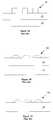
- FIGS. 1 a - 1 cillustrate a conventional microlens formation process.
- a layer of a lens material 20such as silicon dioxide is formed on glass substrate 10 .
- An array of photoresist cylinders 30is formed over the layer of lens material. The photoresist 30 is then heated and reflowed, producing reflowed photoresist bodies 40 as illustrated in FIG. 1 b .
- the surfaces of the bodies 40 formed in thisare virtually spherical.
- Etchingis then performed using a conventional etching process, such as reactive ion etching, that is particularly chosen to provide an approximately 1:1 photoresist to lens material etch ratio.
- a conventional etching processsuch as reactive ion etching, that is particularly chosen to provide an approximately 1:1 photoresist to lens material etch ratio.
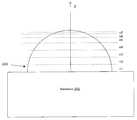
- FIG. 2illustrates the convergence of rays of light exiting the flat base surface of a spherical lens.
- rays 60 exiting from the outermost edges of the lensconverge at a point 62 that is higher than the point of convergence 72 of rays 70 that exit the center of the lens.
- the narrowest spot size that can be produced by the lensoccurs at the plane indicated by line A—A. Even at this plane, only a fraction of the refracted light is fully converged.
- Variations on the conventional techniquemay be employed to produce lenses having aspherical cross-sections.
- aspherical lensescan be formed by gray scale photolithogaphy.
- Aspheric lensescan also be formed by using a variation of the conventional photoresist reflow-and-etch process. In this method, the etch conditions are varied during etching, such that the spherical photoresist body produces an aspherical body in the substrate material.
- Embodiments of the inventionovercome disadvantages of conventional microlenses and microlens fabrication techniques by employing a lens material having a refractive index that varies along its z-axis and shaping the microlens structure from such material by using, for example, conventional microlens shaping techniques.
- the gradient of the refractive index along the z-axisis designed to provide desired refractive properties in conjunction with the lens surface shape. Accordingly, the refractive properties of conventionally shaped microlenses are controlled with great precision through design and manipulation of the refractive properties of the lens material.
- Embodiments of the inventionrelate to a method for designing and fabricating a microlens, wherein a lens surface shape is defined, desired refraction properties of the lens are defined, and a material is formed that has a refractive index gradient in the direction of the z-axis that is determined based upon the desired refraction properties and the defined surface shape of the lens. Further embodiments of the invention relate to a method for fabricating a microlens, wherein a material gradient providing a desired refractive index gradient is determined based upon a lens surface shape and desired refractive parameters, a graded index material having the material gradient is deposited, and a microlens having the desired surface shape is formed in the graded index material. Further embodiments of the invention relate to a microlens structure having a refractive index gradient in the direction of the z-axis for providing predetermined lens refractive properties in conjunction with the lens surface shape.
- the lens materialmay be deposited in a continuous deposition process, in which processing parameters such as deposition gas pressures or flow/evaporation rates are varied continuously to vary the composition of the deposited material layer and thereby vary the refractive index.
- processing parameterssuch as deposition gas pressures or flow/evaporation rates are varied continuously to vary the composition of the deposited material layer and thereby vary the refractive index.
- graded refractive index thin filmsmay be deposited with precision control for a wide range of materials by physical (i.e. evaporation) and chemical vapor deposition (e.g., MOCVD) techniques.
- the lens materialmay be comprised of discrete sub-layers having different refractive indices.
- the lens materialis chosen in accordance with the wavelength of light for which the lens is to be applied.
- Preferred embodiments of the invention for visible wavelength applicationsmay employ silicon oxides SiO X or combinations of SiO and TiO 2 . It is desirable to employ materials that provide a 1:1 etching ratio using a known etching technique.
- Embodiments of the inventionenable formation of lenses in accordance with desired refractive properties.
- a lensmay be designed in accordance with an example embodiment of the invention by determining a desired lens shape, determining a refractive index gradient that will provide the desired convergence, and determining a lens material gradient that will provide the desired refractive index gradient.
- the refractive index gradientmay be determined iteratively to minimize the error of simulated refractive properties relative to ideal desired refractive properties.
- a lensmay be fabricated in accordance with an example embodiment of the invention by forming a lens material layer having a material gradient in the direction of the z-axis in accordance with a design as described above, and etching the material to form microlenses having a desired surface shape.
- Microlenses in accordance with the inventionhave a wide range of applications such as beam steering, coupling, and image display.
- FIGS. 1 a , 1 b and 1 cshow structures in a conventional process for fabricating a microlens array
- FIG. 2shows light ray convergence in a conventional spherical microlens
- FIG. 3shows an example of a microlens in accordance with the invention comprising multiple layers having different refractive indices
- FIG. 4shows an example of a microlens in accordance with an embodiment of the invention having a continuously variable refractive index
- FIG. 5shows a process for designing a lens in accordance with an embodiment of the invention
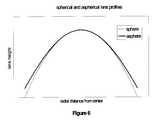
- FIG. 6shows the comparative geometries of a spherical and an aspherical lens surface
- FIG. 7shows an example of the use of the microlens of an embodiment of the invention in a beam steering application.
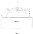
- FIG. 3illustrates a first example of a spherical microlens in accordance with an embodiment the invention.
- the lenscomprises a spherical body 200 formed on a substrate 202 .
- the lens bodyis comprised of seven layers n 1 -n 7 that are stacked vertically above the substrate layer. Each layer is composed of a material that is different in refractive index from the one below it.
- the lowest layer n 1is composed of SiO 2 , which has a relatively low refractive index.
- the highest layer n 7is composed of a SiO 2 /TiO 2 alloy that has a relatively high refractive index.
- the intermediate layers n 2 -n 6are composed of SiO 2 /TiO 2 alloys of varying proportions, with the proportion of SiO 2 being high in layer n 2 and progressively decreasing in succeeding layers.
- the lens body 200thus has a refractive index gradient that increases in the direction of the z-axis normal to the lens substrate. Light entering the lens at any point is refracted one or more times as it passes through the junctions between each layer.
- the layer thicknessesare chosen in accordance with desired refractive properties. In one type of application, the refractive properties may be chosen to provide a desired convergence of light passing through the lens. In another type of application, the layer thicknesses may be made equal to a quarter-wavelength of a given wavelength so that light having the given wavelength will be reflected and therefore dispersed by the curved surface of the lens.
- FIG. 4shows a preferred embodiment of a microlens in accordance with the invention.
- the microlens of FIG. 4has a continuously variable refractive index gradient n(z) that varies as a function of the distance z from the substrate along the z-axis normal to the substrate.
- the lens material at the base of the lensis composed of SiO 2
- the lens material at the apex of the lensis composed of a SiO 2 /TiO 2 alloy with a high refractive index.
- the lens materialis composed of a SiO 2 /TiO 2 alloy that varies in proportions in the direction. of the z-axis.
- the material composition gradient of a microlensmay be determined through a design process as illustrated in FIG. 5 .
- the processcomprises defining 500 the surface shape of the lens body that will be fabricated, determining 502 a refractive index gradient for the lens body that will produce desired refractive properties given the lens surface shape, and determining 504 a material composition gradient providing the desired refractive index gradient. It will be appreciated by those of ordinary skill in the art that the functionality of a design process in accordance with embodiments of the invention may be implemented using a computing device in a variety of different manners.
- the lensis defined to have a spherical surface, such as may be formed using the conventional photoresist reflow technique described above. Desired refractive properties are then defined.
- the lensis desired to provide aberration free focusing at a focal plane that is located a focal length f from the lens.
- a radius of curvature R C of the lensis determined in accordance with the desired focal length f such that:
- nis an average refractive index of the lens. Since the true average refractive index n is not known precisely at this stage of the design process, the value of n is initially assumed to be an average of refractive indices of materials that will presumptively be used at the substrate and at the apex of the lens surface. Thus, for example if the lens of FIG. 4 will use alloys of SiO 2 and TiO 2 , the average refractive index n is the average of the refractive indices of the alloys that are expected to be used at the base and at the apex. Since the design process is iterative, as explained below, erroneous assumptions regarding these values will be corrected in the course of the iterations.
- the angle of refraction ⁇ ′which is the angle of the ray relative to the normal to the surface that is produced as a result of refraction by the lens material, is determined by application of Snell's Law:
- n(z)is the refractive index at the distance z of the point of incidence from the substrate.
- the refractive index gradient function n(z)is assumed to be a polynomial:
- n ( z )n 0 +a*z+b*z 2 +c*Z 3
- 0is the refractive index of the substrate material
- a, b and care coefficients that will be determined through the iterative process.
- the paths of sample rays entering the surface of the lensare determined using Snell's Law and the refractive index provided by the polynomial gradient function.
- the lensmay be treated as being composed of a large number of thin (infinitesimal at the limit) layers parallel to the substrate surface, each with a refractive index which is constant in the thin layer, but different from the neighboring layers in accordance with the function n(z) described above.
- Snell's lawcan be applied once at the incident surface and a second time at the exit surface to determine the direction of the ray after the lens. This method, although not exact, produces a very small error ( ⁇ 1%) in most applications and is computationally much simpler.
- the process described abovemay be altered in a variety of ways.
- the exemplary processdefined a fixed radius of curvature at the outset based on a desired focal length, and determined an optimal gradient for that focal length and radius by feeding back sample ray path errors to the gradient polynomial.
- the processmay be altered such that only the radius of curvature is held constant, or such that only the focal length is held constant.
- the iterative processassumes the use of a spherical lens, other lens surface shapes may be employed.
- the above exampleemploys a polynomial gradient function, other functions such as natural log functions or sine functions can be employed.
- a simple sum of squared errors optimization functionwas employed, alternative optimization functions may also be employed.
- any desired refractive propertiesray positions are determined at the focal plane, and these ray positions are then used in the iterative process for purposes of error determination. In this way, a refractive index profile is determined that achieves the desired ray convergence or divergence.
- a lens having hyperbolic surfaceis desirable for efficiently coupling light to optical fibers, as described in H M Presby, C A Edwards, “Near 100% efficient fiber microlenses”, Elect.
- a refractive gradient indexWhen a refractive gradient index has been determined in accordance with a given lens shape and refractive properties, this information is used to determine a material composition gradient for the lens material layer.
- a variety of materialsare available for refracting different wavelengths. Where the lens body will be formed by etching, it is desirable for the materials used in combination to be capable of a 1:1 etch ratio under given etching conditions.
- Wavelength range MaterialRefractive index range SiO x (1 ⁇ x ⁇ 2) 0.6-2.5 1.45-1.9 SiO 2 —TiO 2 0.4-2.5 1.45-2.15 SiO 2 —Ta 2 O 5 0.4-2.5 1.45-2.05 SiO 2 —ZrO 2 0.4-2.5 1.45-2.1 Ge—ZnS 2.0-16.0 2.26-4.0 ZnS—MgF 2 0.4-6.0 1.35-2.25
- the lens materialis preferably formed in a single continuous processing step.
- the layers n 1 -n 7may be formed sequentially in a single physical or chemical vapor deposition process in which the pressures and/or flow/evaporation rates of source materials are varied at the beginning of each layer to produce the desired composition.
- deposition parametersmay be continuously varied to produce a material gradient providing the predetermined refractive index gradient.
- the deposited materialis continuously monitored using one of the conventional monitoring techniques, such as laser reflectance, spectral reflectance, or ellipsometry.
- the materialis etched to form one or more lens bodies. Etching may be performed in accordance with the conventional processes described above by forming reflowed photoresist bodies above the deposited material and etching using the photoresist bodies as masks in the etching process. For all materials, it is important to use an etching process for which the materials have a 1:1 etch ratio. Further, where it is intended to replicate the shape of the photoresist body in the lens material, it is important to use an etching process for which the deposited material and the photoresist have a 1:1 etch ratio.
- the photoresist bodiesmay be formed directly on the deposited material, or intermediate layers may be employed in accordance with standard semiconductor processing techniques such as the use of antireflective coating (ARC) layers to improve photoresist exposure.
- ARCantireflective coating
- the example abovedescribes the use of a spherical lens formed using the conventional photoresist reflow technique.
- aspherical surfacesmay also be formed by varying the etch rate ratio of the material with respect to photoresist.
- Typical aspheric surfacesdeviate slightly from a sphere and generally have ‘flatter’ curvature at the lens edge.
- FIG. 6compares a spherical surface and an extremely aspherical surface chosen to illustrate the difference
- the base of the lens in the exampleis circular, other base shapes, including square or hexagonal, can also be formed by reflow or gray scale photolithography techniques.
- Gray scale photolithographyuses a spatially variable transmission photomask to ‘photosculp’ the photoresist.
- the gray scale photomaskmay be made, for example, by half-tone design (see, for example, “Method for fabricating microlenses”, U.S. Pat. No. 5,310,623) or using a special HEBSTM photomask material.
- the HEBS photomaskcan be locally darkened (written) by e-beam or laser exposure with varying degrees of grayness depending on the e-beam or laser dose.
- the photoresistthen dissolves in the developer proportionately to the local UV dosage.
- a spatial optical density map in the photomaskis converted to local photoresist height variations after exposure and development.
- the lens structures of the examples described abovewere formed by etching a layer of lens material using a photo mask having the approximate structure of the desired lens.
- An alternative method of fabricating the lens bodyinvolves the process of deposition through a physical aperture.
- a “shadow mask”is disposed between the deposition source and the substrate.
- the shadow maskis typically a thin metal plate having an array of holes formed therein. Deposition through the shadow mask produces bodies of deposited material that are aligned with the holes in the mask. Shadow mask techniques are described in various publications by Grunwald, including R Grunwald, H Mischke, W Rehak, “Microlens formation by thin-film deposition with mesh-shaped masks”, Appl.
- the source materials used in the shadow mask techniquemay be varied as described above to produce a refractive index gradient within the deposited lens bodies. It is noted that in this embodiment, the lens material does not reqiure a 1:1 etch ratio, because the lens shape is defined through the deposition process.
- a reverse processmay be employed. Specifically, given a material that has a refractive index gradient in the direction of the z-axis, a lens shape may be determined for providing desired refractive properties. A lens having the lens shape may then be formed in the material.
- Microlenses in accordance with embodiments of the inventionare useful in a wide variety of applications where optical elements are employed.
- applications that use conventinal microlens arrayssuch as beam steerers (see M W Farn, “Agile beam steering using phased-arraylike binary optics”, Appl. Opt., 33, 5161-5168 (1994), and E Motamedi, A P Andrews, W J Gunning, M Khoshnevisan, “Miniaturized micro-optical scanners”, Opt.
- FIG. 7shows a beam steering device employing microlenses in accordance with an embodiment of the invention.
- the beam steering deviceincludes two opposed microlens arrays 700 , 702 .
- Collimated light, represented by wave fronts 704enters and passes through the first aspheric microlens array 700 and is converged at convergence points 706 .
- the lightsubsequently passes through the second microlens array 702 .
- the individual lens bodies of the microlens arraysare in alignment and so the light exiting the second array 702 , represented by wave fronts 708 , travels in the same direction in which it entered the first array 700 .
- the lightmay be steered by moving either array laterally with respect to the other. For example, when the second array 702 is shifted leftward, the wave fronts exiting the second array 702 rotate clockwise, with the rotation increasing in proportion to the degree by which the array is shifted.
- Field lensesmay be disposed between the two arrays to prevent light leaving one lens body of the first array 700 from straying to a different lens body of the second array 702 .
- aspherical refractionis required because in the off-axis position, i.e. when one lens array is move laterally with respect to the opposing lens array, the rays from the first lenses are incident asymmetrically on the second lenses.
- the appropriate corrective refractive gradientmay be implemented using embodiments of the present invention.
- Microlenses in accordance with further embodiments of the inventionare also useful for coupling of light into high numerical aperture fiber.
- only rays within a certain conewill be accepted into the fiber.
- Other aberrated rayswill come into the fiber opening at too steep an angle and will not undergo total internal reflection at the fiber core-cladding interface and therefore will not be transmitted in the fiber, resulting in insertion loss.
- the optimum lens shape for these applicationsis a hyperbolic shape, which is difficult to fabricate in a microlens using conventional technology.
- an effective hyperbolic profilemay be achieved with a spherical lens body and an appropriate refractive index gradient.
- Microlenses in accordance with further embodiments of the inventionare also useful in detector arrays.
- a detector arrayan a microlens is provided in correspondence with each detector of the array. It is desirable to minimize the cross-talk among individual detector elements. Because it produces a smaller spot size at the focal plane than a conventional microlens, the microlens in accordance with the invention reduces the amount of light leaking to an adjoining detector. Accordingly, a detector array employing a microlens in accordance with the present invention produces images that are sharper in color and in edge acuity.
- microlenses in accordance with the inventionmay be used to provide a high quality wavefront in an exit pupil enhancer.
Landscapes
- Physics & Mathematics (AREA)
- General Physics & Mathematics (AREA)
- Optics & Photonics (AREA)
- Lenses (AREA)
- Surface Treatment Of Glass (AREA)
Abstract
Description
| Wavelength range | ||||
| Material | (microns) | Refractive index range | ||
| SiOx(1 < x < 2) | 0.6-2.5 | 1.45-1.9 | ||
| SiO2—TiO2 | 0.4-2.5 | 1.45-2.15 | ||
| SiO2—Ta2O5 | 0.4-2.5 | 1.45-2.05 | ||
| SiO2—ZrO2 | 0.4-2.5 | 1.45-2.1 | ||
| Ge—ZnS | 2.0-16.0 | 2.26-4.0 | ||
| ZnS—MgF2 | 0.4-6.0 | 1.35-2.25 | ||
Claims (34)
Priority Applications (5)
| Application Number | Priority Date | Filing Date | Title |
|---|---|---|---|
| US09/676,698US6661581B1 (en) | 2000-09-29 | 2000-09-29 | Graded index microlenses and methods of design and formation |
| EP20010973739EP1322977A2 (en) | 2000-09-29 | 2001-09-20 | Graded index microlenses and methods of design and formation |
| PCT/US2001/042228WO2002027360A2 (en) | 2000-09-29 | 2001-09-20 | Graded index microlenses and methods of design and formation |
| CA002420954ACA2420954A1 (en) | 2000-09-29 | 2001-09-20 | Graded index microlenses and methods of design and formation |
| JP2002530883AJP2004510194A (en) | 2000-09-29 | 2001-09-20 | Refractive index distribution type micro lens and design and forming method |
Applications Claiming Priority (1)
| Application Number | Priority Date | Filing Date | Title |
|---|---|---|---|
| US09/676,698US6661581B1 (en) | 2000-09-29 | 2000-09-29 | Graded index microlenses and methods of design and formation |
Publications (1)
| Publication Number | Publication Date |
|---|---|
| US6661581B1true US6661581B1 (en) | 2003-12-09 |
Family
ID=24715601
Family Applications (1)
| Application Number | Title | Priority Date | Filing Date |
|---|---|---|---|
| US09/676,698Expired - LifetimeUS6661581B1 (en) | 2000-09-29 | 2000-09-29 | Graded index microlenses and methods of design and formation |
Country Status (5)
| Country | Link |
|---|---|
| US (1) | US6661581B1 (en) |
| EP (1) | EP1322977A2 (en) |
| JP (1) | JP2004510194A (en) |
| CA (1) | CA2420954A1 (en) |
| WO (1) | WO2002027360A2 (en) |
Cited By (14)
| Publication number | Priority date | Publication date | Assignee | Title |
|---|---|---|---|---|
| US20050208698A1 (en)* | 2004-03-18 | 2005-09-22 | Eastman Kodak Company | Monitoring the deposition properties of an oled |
| US20060170809A1 (en)* | 2005-01-28 | 2006-08-03 | Hon Hai Precision Industry Co., Ltd. | Optical lens module |
| US20070035849A1 (en)* | 2005-08-11 | 2007-02-15 | Jin Li | Method and apparatus providing graded-index microlenses |
| US20070259127A1 (en)* | 2006-05-02 | 2007-11-08 | Sharp Laboratories Of America, Inc. | Method for densifying sol-gel films to form microlens structures |
| US20080080056A1 (en)* | 2006-08-29 | 2008-04-03 | Micron Technology, Inc. | Method and apparatus for reducing microlens surface reflection |
| US20090068775A1 (en)* | 2005-11-28 | 2009-03-12 | Ki-Soo Chang | Method for Fabricating Micro-Lens and Micro-Lens Integrated Optoelectronic Devices Using Selective Etch of Compound Semiconductor |
| US20090109542A1 (en)* | 2007-10-24 | 2009-04-30 | Micron Technology, Inc. | Lens, a lens array and imaging device and system having a lens, and method of forming the same |
| US20100032550A1 (en)* | 2008-08-06 | 2010-02-11 | Young Je Yun | Image sensor and method of manufacturing the same |
| US7701636B2 (en) | 2008-03-06 | 2010-04-20 | Aptina Imaging Corporation | Gradient index microlenses and method of formation |
| CN102027155A (en)* | 2008-03-28 | 2011-04-20 | 圣维可福斯集团有限公司 | A coating and a method for producing a coating |
| US20110198486A1 (en)* | 2005-12-26 | 2011-08-18 | Crosstek Capital, LLC | Image sensor and method for manufacturing the same |
| US20150270303A1 (en)* | 2014-03-19 | 2015-09-24 | SK Hynix Inc. | Image sensor with micro lens |
| CN106662676A (en)* | 2014-10-15 | 2017-05-10 | 微凤凰有限公司 | Method for manufacturing microarray lens |
| US10551633B2 (en) | 2014-09-30 | 2020-02-04 | Kuraray Co., Ltd. | Diffuser plate and method for designing diffuser plate |
Families Citing this family (2)
| Publication number | Priority date | Publication date | Assignee | Title |
|---|---|---|---|---|
| CN100555006C (en)* | 2003-07-01 | 2009-10-28 | 独立行政法人科学技术振兴机构 | Diffraction of light method and diffraction instrument, used diffraction grating, position encoder device |
| JP4208072B2 (en) | 2003-12-05 | 2009-01-14 | シャープ株式会社 | Semiconductor device and manufacturing method thereof |
Citations (12)
| Publication number | Priority date | Publication date | Assignee | Title |
|---|---|---|---|---|
| US4518222A (en)* | 1983-12-08 | 1985-05-21 | Corning Glass Works | Optical device and method |
| US4805997A (en) | 1985-05-31 | 1989-02-21 | Hoya Corporation | Gradient refractive index type anamorphic planar microlens and method of producing the same |
| US4952037A (en) | 1985-03-05 | 1990-08-28 | Nippon Sheet Glass Co., Ltd. | Plate microlens and method for manufacturing the same |
| US5074649A (en) | 1989-07-25 | 1991-12-24 | Nippon Sheet Glass Co., Ltd. | Plate with lens array |
| US5143659A (en)* | 1989-10-04 | 1992-09-01 | Eastman Kodak Company | Method and apparatus for manufacturing aspherically shaped small lenses |
| US5310623A (en) | 1992-11-27 | 1994-05-10 | Lockheed Missiles & Space Company, Inc. | Method for fabricating microlenses |
| US5800666A (en) | 1994-05-16 | 1998-09-01 | Alcatel Network Systems, Inc. | Method and system for forming an optical fiber microlens |
| EP0918235A2 (en) | 1997-11-20 | 1999-05-26 | Nippon Sheet Glass Co., Ltd. | Axial refractive index distributed lens |
| US5926319A (en) | 1993-09-02 | 1999-07-20 | Nashua Corporation | Screens having graded refractive index lenses |
| US6027672A (en) | 1997-12-31 | 2000-02-22 | Lightpath Technologies, Inc. | Method of producing large polymer optical blanks with predictable axil refractive index profile |
| US6107000A (en) | 1996-12-17 | 2000-08-22 | Board Of Regents - University Of California - San Diego | Method for producing micro-optic elements with gray scale mask |
| US20010048968A1 (en)* | 2000-02-16 | 2001-12-06 | Cox W. Royall | Ink-jet printing of gradient-index microlenses |
- 2000
- 2000-09-29USUS09/676,698patent/US6661581B1/ennot_activeExpired - Lifetime
- 2001
- 2001-09-20WOPCT/US2001/042228patent/WO2002027360A2/ennot_activeApplication Discontinuation
- 2001-09-20JPJP2002530883Apatent/JP2004510194A/enactivePending
- 2001-09-20EPEP20010973739patent/EP1322977A2/ennot_activeWithdrawn
- 2001-09-20CACA002420954Apatent/CA2420954A1/ennot_activeAbandoned
Patent Citations (13)
| Publication number | Priority date | Publication date | Assignee | Title |
|---|---|---|---|---|
| US4518222A (en)* | 1983-12-08 | 1985-05-21 | Corning Glass Works | Optical device and method |
| US4952037A (en) | 1985-03-05 | 1990-08-28 | Nippon Sheet Glass Co., Ltd. | Plate microlens and method for manufacturing the same |
| US4805997A (en) | 1985-05-31 | 1989-02-21 | Hoya Corporation | Gradient refractive index type anamorphic planar microlens and method of producing the same |
| US5074649A (en) | 1989-07-25 | 1991-12-24 | Nippon Sheet Glass Co., Ltd. | Plate with lens array |
| US5143659A (en)* | 1989-10-04 | 1992-09-01 | Eastman Kodak Company | Method and apparatus for manufacturing aspherically shaped small lenses |
| US5482800A (en) | 1992-11-27 | 1996-01-09 | Lockheed Missiles & Space Company, Inc. | Exposure mask for fabricating microlenses |
| US5310623A (en) | 1992-11-27 | 1994-05-10 | Lockheed Missiles & Space Company, Inc. | Method for fabricating microlenses |
| US5926319A (en) | 1993-09-02 | 1999-07-20 | Nashua Corporation | Screens having graded refractive index lenses |
| US5800666A (en) | 1994-05-16 | 1998-09-01 | Alcatel Network Systems, Inc. | Method and system for forming an optical fiber microlens |
| US6107000A (en) | 1996-12-17 | 2000-08-22 | Board Of Regents - University Of California - San Diego | Method for producing micro-optic elements with gray scale mask |
| EP0918235A2 (en) | 1997-11-20 | 1999-05-26 | Nippon Sheet Glass Co., Ltd. | Axial refractive index distributed lens |
| US6027672A (en) | 1997-12-31 | 2000-02-22 | Lightpath Technologies, Inc. | Method of producing large polymer optical blanks with predictable axil refractive index profile |
| US20010048968A1 (en)* | 2000-02-16 | 2001-12-06 | Cox W. Royall | Ink-jet printing of gradient-index microlenses |
Non-Patent Citations (13)
| Title |
|---|
| Christopher A. Edwards et al., Ideal Microlenses for Laser to Fiber Coupling, Journal Of Lightwave Technology, vol. 11, No. 2, Feb. 1993, pp. 252-257. |
| D Daly et al., The manufacture of microlenses by melting photoresist, Meas. Sci. Technol., 1, (1990), pp. 759-766. |
| H. M. Presby et al., Near 100% Efficient Fibre Microlenses, Electronics Letters, vol. 28, No. 6, 12<th >Mar. 1992, pp. 582-584. |
| H. M. Presby et al., Near 100% Efficient Fibre Microlenses, Electronics Letters, vol. 28, No. 6, 12th Mar. 1992, pp. 582-584. |
| H. O. Sankur et al., Micromachining Technology for Micro-Optics, SPIE, vol. 4179, Sep. 2000, pp. 30-55. |
| M. Edward Motamedi, Miniaturized micro-optical scanners, Optical Engineering, vol. 33, No. 11, Nov. 1994, pp. 3616-3623. |
| Michael W. Farn, Agile beam steering using phased-arraylike binary optics, Applied Optics, vol. 33, No. 22, Aug. 1, 1994, pp. 5151-5158. |
| PCT International Search Report as issued in International Application No. PCT/US02/42228, Mailing Date Dec. 6, 2002. |
| R Grunwald et al., Thin-film microlens arrays with non-spherical elements, Pure Appl. Opt., 6 (1997), pp. 663-671. |
| Robert H. Dueck et al., Optical design with inhomogeneous glass: The future is here, SPIE, vol. 3130, Jul. 1997, pp. 32-40. |
| Rudiger Grunwald et al., Axial Beam Shaping with Nonspherical Microoptics, Jpn. J. Appl. Phys., vol. 37, (1998) Pt. 1, No. 6B, Jun. 1998, pp. 3701-3707. |
| Ruediger Grunwald et al., Microlens formation by thin-film deposition with mesh-shaped masks, Applied Optics, vol. 38, No. 19, Jul. 1, 1999, pp. 4117-4124. |
| Zoran D. Popovic et al., Technique for monolithic fabrication of microlens arrays, Applied Optics, vol. 27, No. 7, Apr. 1, 1998, pp. 1281-1284. |
Cited By (28)
| Publication number | Priority date | Publication date | Assignee | Title |
|---|---|---|---|---|
| US7214554B2 (en)* | 2004-03-18 | 2007-05-08 | Eastman Kodak Company | Monitoring the deposition properties of an OLED |
| US20050208698A1 (en)* | 2004-03-18 | 2005-09-22 | Eastman Kodak Company | Monitoring the deposition properties of an oled |
| US20060170809A1 (en)* | 2005-01-28 | 2006-08-03 | Hon Hai Precision Industry Co., Ltd. | Optical lens module |
| US7522353B2 (en)* | 2005-01-28 | 2009-04-21 | Hon Hai Precision Industry Co., Ltd. | Optical lens module |
| US7564631B2 (en) | 2005-08-11 | 2009-07-21 | Aptina Imaging Corporation | Method and apparatus providing graded-index microlenses |
| US20070035849A1 (en)* | 2005-08-11 | 2007-02-15 | Jin Li | Method and apparatus providing graded-index microlenses |
| US20070035847A1 (en)* | 2005-08-11 | 2007-02-15 | Micron Technology, Inc. | Method and apparatus providing graded-index microlenses |
| US20070217020A1 (en)* | 2005-08-11 | 2007-09-20 | Jin Li | Method and apparatus providing graded-index microlenses |
| US7317579B2 (en)* | 2005-08-11 | 2008-01-08 | Micron Technology, Inc. | Method and apparatus providing graded-index microlenses |
| US7473378B2 (en) | 2005-08-11 | 2009-01-06 | Aptina Imaging Corporation | Method and apparatus providing graded-index microlenses |
| US8021903B2 (en)* | 2005-11-28 | 2011-09-20 | Ytel Photonics Inc. | Method for fabricating micro-lens and micro-lens integrated optoelectronic devices using selective etch of compound semiconductor |
| US20090068775A1 (en)* | 2005-11-28 | 2009-03-12 | Ki-Soo Chang | Method for Fabricating Micro-Lens and Micro-Lens Integrated Optoelectronic Devices Using Selective Etch of Compound Semiconductor |
| US8287948B2 (en)* | 2005-12-26 | 2012-10-16 | Intellectual Ventures Ii Llc | Image sensor and method for manufacturing the same |
| US8846433B2 (en) | 2005-12-26 | 2014-09-30 | Intellectual Ventures Ii Llc | Image sensor and method for manufacturing the same |
| US20110198486A1 (en)* | 2005-12-26 | 2011-08-18 | Crosstek Capital, LLC | Image sensor and method for manufacturing the same |
| US20070259127A1 (en)* | 2006-05-02 | 2007-11-08 | Sharp Laboratories Of America, Inc. | Method for densifying sol-gel films to form microlens structures |
| US20080080056A1 (en)* | 2006-08-29 | 2008-04-03 | Micron Technology, Inc. | Method and apparatus for reducing microlens surface reflection |
| US7724439B2 (en) | 2007-10-24 | 2010-05-25 | Aptina Imaging Corporation | Lens, a lens array and imaging device and system having a lens, and method of forming the same |
| US20090109542A1 (en)* | 2007-10-24 | 2009-04-30 | Micron Technology, Inc. | Lens, a lens array and imaging device and system having a lens, and method of forming the same |
| US7701636B2 (en) | 2008-03-06 | 2010-04-20 | Aptina Imaging Corporation | Gradient index microlenses and method of formation |
| US20110097551A1 (en)* | 2008-03-28 | 2011-04-28 | Kaj Pischow | Coating and a method for producing a coating |
| CN102027155A (en)* | 2008-03-28 | 2011-04-20 | 圣维可福斯集团有限公司 | A coating and a method for producing a coating |
| US20100032550A1 (en)* | 2008-08-06 | 2010-02-11 | Young Je Yun | Image sensor and method of manufacturing the same |
| US20150270303A1 (en)* | 2014-03-19 | 2015-09-24 | SK Hynix Inc. | Image sensor with micro lens |
| US9673242B2 (en)* | 2014-03-19 | 2017-06-06 | SK Hynix Inc. | Image sensor with micro lens including a plurality of layers each of different thickness |
| US10551633B2 (en) | 2014-09-30 | 2020-02-04 | Kuraray Co., Ltd. | Diffuser plate and method for designing diffuser plate |
| US11378812B2 (en) | 2014-09-30 | 2022-07-05 | Kuraray Co., Ltd. | Diffuser plate and method for designing diffuser plate |
| CN106662676A (en)* | 2014-10-15 | 2017-05-10 | 微凤凰有限公司 | Method for manufacturing microarray lens |
Also Published As
| Publication number | Publication date |
|---|---|
| JP2004510194A (en) | 2004-04-02 |
| WO2002027360A2 (en) | 2002-04-04 |
| CA2420954A1 (en) | 2002-04-04 |
| EP1322977A2 (en) | 2003-07-02 |
| WO2002027360A3 (en) | 2003-03-13 |
Similar Documents
| Publication | Publication Date | Title |
|---|---|---|
| US6661581B1 (en) | Graded index microlenses and methods of design and formation | |
| US20230194760A1 (en) | Hybrid optical system having superlens and refraction and/or reflection lens | |
| US5731899A (en) | Lenslet array system incorporating an integral field lens/reimager lenslet array | |
| US5796522A (en) | Lenslet array system with a baffle structure and a shutter | |
| US7019918B2 (en) | Panoramic imaging system | |
| US5822125A (en) | Lenslet array system | |
| US5541774A (en) | Segmented axial gradient lens | |
| US4896952A (en) | Thin film beamsplitter optical element for use in an image-forming lens system | |
| US6829093B1 (en) | Diffraction optical element | |
| US7554735B2 (en) | Diffractive optical element and optical system including the same | |
| US11536882B2 (en) | Method of fabricating an imaging system and corresponding imaging system | |
| US20010024330A1 (en) | Catadioptric reduction projection optical system | |
| US5812322A (en) | Lenslet array system incorporating a field lenslet array | |
| CN114488519A (en) | Diffraction optical lens with continuously adjustable large-angle incident focal length and design method thereof | |
| US6271975B1 (en) | Light collecting optical device forming a multiple focal distance lens | |
| JPH04215610A (en) | Element of single-hybrid reflecting and refracting optical system | |
| US6903877B2 (en) | Gradient-index lens, and method for producing the same | |
| US5223978A (en) | Hybrid diffractive/refractive lens | |
| US6965483B2 (en) | Imaging system comprising a concave mirror | |
| CN108709639A (en) | Imaging spectrometer based on reflective prism-grating beam splitting module | |
| JP3467018B2 (en) | Optical system and optical equipment | |
| JPH11316338A (en) | Design method of lens and optical system | |
| JP3052528B2 (en) | Optical lens and manufacturing method thereof | |
| US11898907B1 (en) | Freeform offner spectrometer | |
| CN208999588U (en) | A Phase-Encoded Fresnel Lens for Imaging |
Legal Events
| Date | Code | Title | Description |
|---|---|---|---|
| AS | Assignment | Owner name:ROCKWELL TECHNOLOGIES, LLC, CALIFORNIA Free format text:ASSIGNMENT OF ASSIGNORS INTEREST;ASSIGNOR:SANKUR, HALUK;REEL/FRAME:011161/0943 Effective date:20000927 | |
| STCF | Information on status: patent grant | Free format text:PATENTED CASE | |
| AS | Assignment | Owner name:INNOVATIVE TECHNOLOGY LICENSING, LLC, CALIFORNIA Free format text:CHANGE OF NAME;ASSIGNOR:ROCKWELL TECHNOLOGIES, LLC;REEL/FRAME:018160/0240 Effective date:20010628 Owner name:ROCKWELL SCIENTIFIC LICENSING, LLC, CALIFORNIA Free format text:CHANGE OF NAME;ASSIGNOR:INNOVATIVE TECHNOLOGY LICENSING, LLC;REEL/FRAME:018160/0250 Effective date:20030919 | |
| AS | Assignment | Owner name:TELEDYNE LICENSING, LLC, CALIFORNIA Free format text:CHANGE OF NAME;ASSIGNOR:ROCKWELL SCIENTIFIC LICENSING, LLC;REEL/FRAME:018573/0649 Effective date:20060918 | |
| FPAY | Fee payment | Year of fee payment:4 | |
| FPAY | Fee payment | Year of fee payment:8 | |
| AS | Assignment | Owner name:TELEDYNE SCIENTIFIC & IMAGING, LLC, CALIFORNIA Free format text:MERGER;ASSIGNOR:TELEDYNE LICENSING, LLC;REEL/FRAME:027830/0206 Effective date:20111221 | |
| FPAY | Fee payment | Year of fee payment:12 |