US6661068B2 - Semiconductor device and method of providing regions of low substrate capacitance - Google Patents
Semiconductor device and method of providing regions of low substrate capacitanceDownload PDFInfo
- Publication number
- US6661068B2 US6661068B2US10/102,505US10250502AUS6661068B2US 6661068 B2US6661068 B2US 6661068B2US 10250502 AUS10250502 AUS 10250502AUS 6661068 B2US6661068 B2US 6661068B2
- Authority
- US
- United States
- Prior art keywords
- semiconductor
- semiconductor device
- isolation region
- pillar
- electrical component
- Prior art date
- Legal status (The legal status is an assumption and is not a legal conclusion. Google has not performed a legal analysis and makes no representation as to the accuracy of the status listed.)
- Expired - Lifetime
Links
- 239000004065semiconductorSubstances0.000titleclaimsabstractdescription73
- 239000000758substrateSubstances0.000titleclaimsdescription19
- 238000000034methodMethods0.000titledescription5
- 239000000463materialSubstances0.000claimsabstractdescription27
- 238000002955isolationMethods0.000claimsabstractdescription20
- 239000003989dielectric materialSubstances0.000claimsabstractdescription14
- 239000011800void materialSubstances0.000claimsabstractdescription13
- VYPSYNLAJGMNEJ-UHFFFAOYSA-NSilicium dioxideChemical compoundO=[Si]=OVYPSYNLAJGMNEJ-UHFFFAOYSA-N0.000claimsdescription22
- 235000012239silicon dioxideNutrition0.000claimsdescription11
- 239000000377silicon dioxideSubstances0.000claimsdescription11
- XUIMIQQOPSSXEZ-UHFFFAOYSA-NSiliconChemical compound[Si]XUIMIQQOPSSXEZ-UHFFFAOYSA-N0.000claimsdescription5
- 229910052710siliconInorganic materials0.000claimsdescription5
- 239000010703siliconSubstances0.000claimsdescription5
- 229910052581Si3N4Inorganic materials0.000claimsdescription4
- HQVNEWCFYHHQES-UHFFFAOYSA-Nsilicon nitrideChemical compoundN12[Si]34N5[Si]62N3[Si]51N64HQVNEWCFYHHQES-UHFFFAOYSA-N0.000claimsdescription4
- 229910021421monocrystalline siliconInorganic materials0.000claimsdescription2
- 239000010410layerSubstances0.000description25
- 238000004519manufacturing processMethods0.000description21
- 230000003071parasitic effectEffects0.000description6
- 230000015572biosynthetic processEffects0.000description3
- 238000005530etchingMethods0.000description3
- XKRFYHLGVUSROY-UHFFFAOYSA-NArgonChemical compound[Ar]XKRFYHLGVUSROY-UHFFFAOYSA-N0.000description2
- 230000007547defectEffects0.000description2
- 239000007789gasSubstances0.000description2
- 230000003647oxidationEffects0.000description2
- 238000007254oxidation reactionMethods0.000description2
- 238000000623plasma-assisted chemical vapour depositionMethods0.000description2
- 230000002787reinforcementEffects0.000description2
- 229910052786argonInorganic materials0.000description1
- 239000003990capacitorSubstances0.000description1
- 239000011248coating agentSubstances0.000description1
- 238000000576coating methodMethods0.000description1
- 238000004891communicationMethods0.000description1
- 239000000356contaminantSubstances0.000description1
- 235000012489doughnutsNutrition0.000description1
- 230000000694effectsEffects0.000description1
- 238000005516engineering processMethods0.000description1
- QKCGXXHCELUCKW-UHFFFAOYSA-Nn-[4-[4-(dinaphthalen-2-ylamino)phenyl]phenyl]-n-naphthalen-2-ylnaphthalen-2-amineChemical compoundC1=CC=CC2=CC(N(C=3C=CC(=CC=3)C=3C=CC(=CC=3)N(C=3C=C4C=CC=CC4=CC=3)C=3C=C4C=CC=CC4=CC=3)C3=CC4=CC=CC=C4C=C3)=CC=C21QKCGXXHCELUCKW-UHFFFAOYSA-N0.000description1
- 238000000059patterningMethods0.000description1
- 229920002120photoresistant polymerPolymers0.000description1
- 238000000926separation methodMethods0.000description1
- 239000002356single layerSubstances0.000description1
Images


Classifications
- H—ELECTRICITY
- H10—SEMICONDUCTOR DEVICES; ELECTRIC SOLID-STATE DEVICES NOT OTHERWISE PROVIDED FOR
- H10D—INORGANIC ELECTRIC SEMICONDUCTOR DEVICES
- H10D84/00—Integrated devices formed in or on semiconductor substrates that comprise only semiconducting layers, e.g. on Si wafers or on GaAs-on-Si wafers
- H—ELECTRICITY
- H01—ELECTRIC ELEMENTS
- H01L—SEMICONDUCTOR DEVICES NOT COVERED BY CLASS H10
- H01L21/00—Processes or apparatus adapted for the manufacture or treatment of semiconductor or solid state devices or of parts thereof
- H01L21/70—Manufacture or treatment of devices consisting of a plurality of solid state components formed in or on a common substrate or of parts thereof; Manufacture of integrated circuit devices or of parts thereof
- H01L21/71—Manufacture of specific parts of devices defined in group H01L21/70
- H01L21/76—Making of isolation regions between components
- H01L21/764—Air gaps
- H—ELECTRICITY
- H10—SEMICONDUCTOR DEVICES; ELECTRIC SOLID-STATE DEVICES NOT OTHERWISE PROVIDED FOR
- H10D—INORGANIC ELECTRIC SEMICONDUCTOR DEVICES
- H10D62/00—Semiconductor bodies, or regions thereof, of devices having potential barriers
- H10D62/10—Shapes, relative sizes or dispositions of the regions of the semiconductor bodies; Shapes of the semiconductor bodies
- H10D62/113—Isolations within a component, i.e. internal isolations
- H10D62/115—Dielectric isolations, e.g. air gaps
Definitions
- the present inventionrelates in general to semiconductor devices and, more particularly, to integrated circuits having components formed on a low capacitance region of a semiconductor die.
- a variety of techniqueshave been tried to reduce the parasitic capacitances of passive integrated circuit components.
- One such techniqueis to form the components over a low permittivity material.
- current low permittivity materialsare limited to film thicknesses that are too thin to produce an adequate reduction in parasitic capacitance.
- Another approachis to form the components over a thick dielectric film in which are formed air gaps or voids that reduce the overall permittivity of the dielectric film.
- previous films made with such voidsintroduce substantial stress in a semiconductor substrate, which degrades the performance and reliability of the integrated circuit.
- Other schemesreduce the stress by producing fewer voids or voids with only a limited volume, which has a correspondingly limited effect on parasitic capacitance.
- Another issue with previous arthas been the high costs associated with the complex patterning and etching steps to produce isolation structures with large void to pillar ratios.
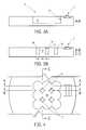
- FIG. 1Ais a first cross-sectional view of a semiconductor device after a first fabrication stage
- FIG. 1Bis a second cross-sectional view of the semiconductor device after the first fabrication stage
- FIG. 2is a top view of the semiconductor device after the first fabrication stage
- FIG. 3Ais a first cross-sectional view of the semiconductor device after a second fabrication stage
- FIG. 3Bis a second cross-sectional view of the semiconductor device after the second fabrication stage
- FIG. 4is a top view of the semiconductor device after the second fabrication stage
- FIG. 5Ais a first cross-sectional view of the semiconductor device after a third fabrication stage
- FIG. 5Bis a second cross-sectional view of the semiconductor device after the third fabrication stage
- FIG. 6is a top view of the semiconductor device after the third fabrication stage
- FIG. 7Ais a top view of a first alternate embodiment of the semiconductor device
- FIG. 7Bis a top view of a second alternate embodiment of the semiconductor device.
- FIG. 7Cis a top view of a third alternate embodiment of the semiconductor device.
- FIG. 7Dis a top view of a fourth alternate embodiment of the semiconductor device.
- FIG. 7Eis a top view of a fifth alternate embodiment of the semiconductor device.
- FIGS. 1A, 1 B, and 2are used to describe a first processing stage, and should be referred to collectively for the description, which follows.
- FIG. 1Ais a first cross-sectional view AA of a semiconductor device 1 after a first fabrication stage
- FIG. 1Bis a second cross-sectional view BB and/or CC of semiconductor device 1 after the first fabrication stage
- FIG. 2is a top view of semiconductor device 1 after the first fabrication stage.
- Semiconductor device or structure 1is formed with a semiconductor substrate material 10 and includes an isolation region 5 for forming electrical components such as passive devices and bonding pads.
- Semiconductor device 1further includes an active region 2 for forming a transistor 3 and/or other active devices.
- semiconductor substrate material 10comprises monocrystalline silicon.
- semiconductor substrate material 10is shown as a single layer. However, semiconductor substrate material 10 typically includes a series of layers for producing active devices in region 2 such as base, epitaxial, and dielectric layers (not shown).
- a surface 12 of semiconductor substrate material 10is patterned with photoresist to mask an series of standard etch steps that remove exposed portions of the dielectric layers described above (not shown).
- a standard anisotropic silicon etchis then applied to remove exposed portions of the epitaxial layer and base layer (not shown) to forms an array of cavities 18 within isolation region 5 .
- cavities 18are formed to a depth 14 of about five micrometers, a width 13 of about one micrometer and about one micrometer of separation 9 between adjacent cavities 18 using a standard silicon reactive ion etch with nitrogen trifluoride gas for about seven minutes.
- Semiconductor device 1is then thermally oxidized to simultaneously grow an extrinsic layer 23 of silicon dioxide on the sidewalls 19 of cavities 18 , which, formed having a thermally grown silicon dioxide which oxidizes the sidewalls 19 of the cavities 18 simultaneously adding silicon dioxide 23 to the sidewalls and consumes a portion of sidewalls 19 to form an intrinsic layer 22 of silicon dioxide.
- a portion 24 of the cavities 18is not filled with silicon dioxide.
- overlapping regions 26 of consumed portions or intrinsic layer 22are formed.
- layer 22 and layer 23constitute a homogeneous or single continuous layer. Note that the pillars 15 of semiconductor substrate material 10 are not consumed by the formation of intrinsic layer 22 . Thus a contiguos?
- homogeneous or single continuous layer of silicon dioxide comprised of extrinsic layer 23 and intrinsic layer 22is formed surrounding pillars 15 of semiconductor material. Since the oxidation rate of semiconductor material is well established and easily controlled, the dimensions of the pillars 15 can be easily controlled.
- FIGS. 3A, 3 B, and 4are used to describe a second processing stage, and should be referred to collectively for the description, which follows.
- FIG. 3Ais a first cross-sectional view AA of semiconductor device 1 after a second fabrication stage
- FIG. 3Bis a second cross-sectional view BB and/or CC of semiconductor device 1 after the second fabrication stage
- FIG. 4is a top view of semiconductor device 1 after the second fabrication stage.
- Semiconductor substrate material 10is subjected to an etch step to remove portion of extrinsic layer 23 and intrinsic layer 22 .
- the etchis performed by a timed wet etch of buffered oxide etch solution for about ten minutes.
- a portion (not shown) of intrinsic layer 22can be left as an etch stop or reinforcement material by reducing the amount of the material removed by the etch, as long as an overlapping region 26 is removed to form the pillars 15 .
- the pillars 15are now left free standing in a recessed region 30 .
- a problem of the prior arthas been controlling etch processes used to form a small pillar in a recess.
- the recessed regionsget large in relation to the pillar, the lack of controllability results In a missing, deformed, or weakened pillar. These defects reduce production yields and increase manufacturing costs.
- advanced photolithographic and etching equipment required to form a small pillaris expensive to purchase, operate and maintain.
- the feature size or width 28 of the pillar 15is primarily determined by the easily controlled oxidation rate of the semiconductor substrate material 10 , rather than the etch rate of the semiconductor substrate material 10 . This enables use of less expensive photolithographic and etching tools to form feature sizes which are smaller than the photolithographic capabilities of the tools, while easily controlling the process to produce a pillar with fewer defects.
- FIGS. 5A, 5 B, and 6are used to describe a third processing stage, and should be referred to collectively for the description, which follows.
- FIG. 5Ais a first cross-sectional view AA of semiconductor device 1 after a third fabrication stage
- FIG. 5Bis a second cross-sectional view BB and/or CC of semiconductor device 1 after the third fabrication stage
- FIG. 6is a top view of semiconductor device 1 after the third fabrication stage.
- a dielectric layer 21is formed in recessed region
- dielectric layer 21is formed to a thickness of about five hundred angstroms of thermally grown silicon dioxide. In an alternate embodiment, dielectric layer 21 is formed of silicon nitride to a thickness of approximately five hundred angstroms.
- a cap layer or dielectric material 20is deposited on substrate surface 12 capping pillars 15 to form a seal over recessed region 30 creating void 16 .
- dielectric material 20is formed of plasma enhanced chemical vapor deposition (PECVD) silicon dioxide to a thickness of approximately ten thousand angstroms.
- PECVDplasma enhanced chemical vapor deposition
- dielectric material 20is formed of silicon nitride to a thickness of approximately ten thousand angstroms.
- void 16has a depth 17 beneath surface 12 of approximately five micrometers.
- Void 16is so designated because it is filled with a gaseous material, which in one embodiment may be air. Void 16 may also be filled with argon or another ambient gas which is present when opening 34 of recessed region 30 becomes sealed off.
- An electrical component 25is formed on dielectric material 20 over isolation region 5 .
- Electrical component 25may be a bonding pad, a passive component such as an inductor, capacitor or resistor, or another electrical device suitable for formation over a dielectric material.
- the effective dielectric constant of isolation region 5is a combination of the dielectric constant or permittivity of void 16 and the permittivity of the materials used to form pillars 15 and dielectric material 21 .
- the gaseous material contained in void 16has a dielectric constant substantially equal to one, and dielectric material 21 has a dielectric constant of about 3.8, thus the overall dielectric constant of the isolation region formed is less than 3.8, depending on the relative volumes of the pillars 15 , dielectric material 21 and void 16 .
- Electrical component 25has a low parasitic capacitance to substrate 10 , and therefore a higher frequency capability, because of the low permittivity of isolation region 5 .
- isolation region 5has a low effective permittivity for forming electrical components with a low parasitic substrate capacitance.
- FIG. 1 through FIG. 6show pillars 15 as being formed using circular cavities 18
- FIGS. 7A through 7Eare used to show some of the many alternate embodiments of the invention possible by varying the shape and quantity of cavities 18 used to subsequently form pillars 15 .
- FIG. 7Ashows an embodiment having a single donut shaped cavity 18 in which pillar 15 is formed.
- FIG. 7Bshows an embodiment having a u-shaped cavity 18 in which pillar 15 is formed using the invention.
- FIG. 7Cshows an embodiment having multiple triangle shaped cavities 18 in which pillar 15 is formed.
- FIG. 7Dshows an embodiment having multiple staggered cavities 18 in which pillars 15 are formed.
- FIG. 7Eshows an embodiment having a multiplicity of u-shaped cavities 18 in which pillars 15 are formed using the invention.
- the present inventionprovides a semiconductor structure ( 1 ), comprising a isolation region ( 5 ) formed above a semiconductor material ( 10 ) with a pillar ( 15 ) formed of the semiconductor material under the isolation region.
- the pillaris capped with a dielectric material ( 20 ) to form a void.
Landscapes
- Engineering & Computer Science (AREA)
- Physics & Mathematics (AREA)
- Condensed Matter Physics & Semiconductors (AREA)
- General Physics & Mathematics (AREA)
- Manufacturing & Machinery (AREA)
- Computer Hardware Design (AREA)
- Microelectronics & Electronic Packaging (AREA)
- Power Engineering (AREA)
- Element Separation (AREA)
- Semiconductor Integrated Circuits (AREA)
Abstract
Description
Claims (15)
Priority Applications (5)
| Application Number | Priority Date | Filing Date | Title |
|---|---|---|---|
| US10/102,505US6661068B2 (en) | 2002-03-20 | 2002-03-20 | Semiconductor device and method of providing regions of low substrate capacitance |
| CNB031073050ACN100336195C (en) | 2002-03-20 | 2003-03-19 | Semiconductor device and method for providing low substrate capacitor area |
| TW092106047ATWI270169B (en) | 2002-03-20 | 2003-03-19 | Semiconductor device and method of providing regions of low substrate capacitance |
| US10/632,636US6818525B1 (en) | 2002-03-20 | 2003-08-04 | Semiconductor device and method of providing regions of low substrate capacitance |
| HK04101821.9AHK1058999B (en) | 2002-03-20 | 2004-03-12 | Semiconductor device and method of providing regions of low substrate capacitance |
Applications Claiming Priority (1)
| Application Number | Priority Date | Filing Date | Title |
|---|---|---|---|
| US10/102,505US6661068B2 (en) | 2002-03-20 | 2002-03-20 | Semiconductor device and method of providing regions of low substrate capacitance |
Related Child Applications (1)
| Application Number | Title | Priority Date | Filing Date |
|---|---|---|---|
| US10/632,636DivisionUS6818525B1 (en) | 2002-03-20 | 2003-08-04 | Semiconductor device and method of providing regions of low substrate capacitance |
Publications (2)
| Publication Number | Publication Date |
|---|---|
| US20030189238A1 US20030189238A1 (en) | 2003-10-09 |
| US6661068B2true US6661068B2 (en) | 2003-12-09 |
Family
ID=28040232
Family Applications (2)
| Application Number | Title | Priority Date | Filing Date |
|---|---|---|---|
| US10/102,505Expired - LifetimeUS6661068B2 (en) | 2002-03-20 | 2002-03-20 | Semiconductor device and method of providing regions of low substrate capacitance |
| US10/632,636Expired - LifetimeUS6818525B1 (en) | 2002-03-20 | 2003-08-04 | Semiconductor device and method of providing regions of low substrate capacitance |
Family Applications After (1)
| Application Number | Title | Priority Date | Filing Date |
|---|---|---|---|
| US10/632,636Expired - LifetimeUS6818525B1 (en) | 2002-03-20 | 2003-08-04 | Semiconductor device and method of providing regions of low substrate capacitance |
Country Status (3)
| Country | Link |
|---|---|
| US (2) | US6661068B2 (en) |
| CN (1) | CN100336195C (en) |
| TW (1) | TWI270169B (en) |
Cited By (7)
| Publication number | Priority date | Publication date | Assignee | Title |
|---|---|---|---|---|
| US6917091B2 (en) | 2003-03-28 | 2005-07-12 | Mitsubishi Denki Kabushiki Kaisha | High power semiconductor device having source electrodes connected by air bridges and having opposite current path directions |
| US20050173777A1 (en)* | 2004-02-09 | 2005-08-11 | Semiconductor Components Industries, Llc | Semiconductor device having reduced capacitance to substrate and method |
| US20070090434A1 (en)* | 2004-01-10 | 2007-04-26 | Hvvi Semiconductors, Inc. | Power semiconductor device and method therefor |
| US20080048215A1 (en)* | 2006-08-25 | 2008-02-28 | Robert Bruce Davies | Electrical stress protection apparatus and method of manufacture |
| US20080142923A1 (en)* | 2006-12-15 | 2008-06-19 | Hvvi Semiconductors, Inc. | Semiconductor structure and method of manufacture |
| US8530963B2 (en) | 2005-01-06 | 2013-09-10 | Estivation Properties Llc | Power semiconductor device and method therefor |
| US20170162927A1 (en)* | 2014-05-31 | 2017-06-08 | Hatem Mohamed Aead | Air Gap Creation In Electronic Devices |
Families Citing this family (5)
| Publication number | Priority date | Publication date | Assignee | Title |
|---|---|---|---|---|
| US8492260B2 (en) | 2010-08-30 | 2013-07-23 | Semionductor Components Industries, LLC | Processes of forming an electronic device including a feature in a trench |
| US8981533B2 (en) | 2012-09-13 | 2015-03-17 | Semiconductor Components Industries, Llc | Electronic device including a via and a conductive structure, a process of forming the same, and an interposer |
| US9812354B2 (en) | 2015-05-15 | 2017-11-07 | Semiconductor Components Industries, Llc | Process of forming an electronic device including a material defining a void |
| US10115790B2 (en) | 2015-09-17 | 2018-10-30 | Semiconductor Components Industries, Llc | Electronic device including an insulating structure |
| US10497602B2 (en) | 2016-08-01 | 2019-12-03 | Semiconductor Components Industries, Llc | Process of forming an electronic device including forming an electronic component and removing a portion of a substrate |
Citations (7)
| Publication number | Priority date | Publication date | Assignee | Title |
|---|---|---|---|---|
| US5324683A (en)* | 1993-06-02 | 1994-06-28 | Motorola, Inc. | Method of forming a semiconductor structure having an air region |
| US5742091A (en) | 1995-07-12 | 1998-04-21 | National Semiconductor Corporation | Semiconductor device having a passive device formed over one or more deep trenches |
| US5844299A (en) | 1997-01-31 | 1998-12-01 | National Semiconductor Corporation | Integrated inductor |
| US6180995B1 (en) | 1999-05-06 | 2001-01-30 | Spectrian Corporation | Integrated passive devices with reduced parasitic substrate capacitance |
| US6221727B1 (en) | 1999-08-30 | 2001-04-24 | Chartered Semiconductor Manufacturing Ltd. | Method to trap air at the silicon substrate for improving the quality factor of RF inductors in CMOS technology |
| US6307247B1 (en) | 1999-07-12 | 2001-10-23 | Robert Bruce Davies | Monolithic low dielectric constant platform for passive components and method |
| US6531376B1 (en)* | 2002-04-17 | 2003-03-11 | Semiconductor Components Industries Llc | Method of making a semiconductor device with a low permittivity region |
Family Cites Families (1)
| Publication number | Priority date | Publication date | Assignee | Title |
|---|---|---|---|---|
| US5240875A (en)* | 1992-08-12 | 1993-08-31 | North American Philips Corporation | Selective oxidation of silicon trench sidewall |
- 2002
- 2002-03-20USUS10/102,505patent/US6661068B2/ennot_activeExpired - Lifetime
- 2003
- 2003-03-19CNCNB031073050Apatent/CN100336195C/ennot_activeExpired - Fee Related
- 2003-03-19TWTW092106047Apatent/TWI270169B/ennot_activeIP Right Cessation
- 2003-08-04USUS10/632,636patent/US6818525B1/ennot_activeExpired - Lifetime
Patent Citations (7)
| Publication number | Priority date | Publication date | Assignee | Title |
|---|---|---|---|---|
| US5324683A (en)* | 1993-06-02 | 1994-06-28 | Motorola, Inc. | Method of forming a semiconductor structure having an air region |
| US5742091A (en) | 1995-07-12 | 1998-04-21 | National Semiconductor Corporation | Semiconductor device having a passive device formed over one or more deep trenches |
| US5844299A (en) | 1997-01-31 | 1998-12-01 | National Semiconductor Corporation | Integrated inductor |
| US6180995B1 (en) | 1999-05-06 | 2001-01-30 | Spectrian Corporation | Integrated passive devices with reduced parasitic substrate capacitance |
| US6307247B1 (en) | 1999-07-12 | 2001-10-23 | Robert Bruce Davies | Monolithic low dielectric constant platform for passive components and method |
| US6221727B1 (en) | 1999-08-30 | 2001-04-24 | Chartered Semiconductor Manufacturing Ltd. | Method to trap air at the silicon substrate for improving the quality factor of RF inductors in CMOS technology |
| US6531376B1 (en)* | 2002-04-17 | 2003-03-11 | Semiconductor Components Industries Llc | Method of making a semiconductor device with a low permittivity region |
Cited By (17)
| Publication number | Priority date | Publication date | Assignee | Title |
|---|---|---|---|---|
| US6917091B2 (en) | 2003-03-28 | 2005-07-12 | Mitsubishi Denki Kabushiki Kaisha | High power semiconductor device having source electrodes connected by air bridges and having opposite current path directions |
| US7898057B2 (en) | 2004-01-10 | 2011-03-01 | Hvvi Semiconductors, Inc. | Radio frequency power semiconductor device package comprising dielectric platform and shielding plate |
| US20070090434A1 (en)* | 2004-01-10 | 2007-04-26 | Hvvi Semiconductors, Inc. | Power semiconductor device and method therefor |
| US9865590B2 (en) | 2004-01-10 | 2018-01-09 | Xenogenic Development Limited Liability Company | Power semiconductor device and method therefor |
| US9177866B2 (en) | 2004-01-10 | 2015-11-03 | Estivation Properties Llc | Power semiconductor device and method therefor |
| US9029946B2 (en) | 2004-01-10 | 2015-05-12 | Estivation Properties Llc | Power semiconductor device and method therefor |
| US7847369B2 (en) | 2004-01-10 | 2010-12-07 | Hvvi Semiconductors, Inc. | Radio frequency power semiconductor device comprising matrix of cavities as dielectric isolation structure |
| US8471378B2 (en) | 2004-01-10 | 2013-06-25 | Estivation Properties Llc | Power semiconductor device and method therefor |
| US20050173777A1 (en)* | 2004-02-09 | 2005-08-11 | Semiconductor Components Industries, Llc | Semiconductor device having reduced capacitance to substrate and method |
| US7087925B2 (en) | 2004-02-09 | 2006-08-08 | Semiconductor Components Industries, L.L.C. | Semiconductor device having reduced capacitance to substrate and method |
| US8530963B2 (en) | 2005-01-06 | 2013-09-10 | Estivation Properties Llc | Power semiconductor device and method therefor |
| US20100103578A1 (en)* | 2006-08-25 | 2010-04-29 | Hvvi Semiconductors, Inc. | Electrical stress protection apparatus and method of manufacture |
| US7656003B2 (en) | 2006-08-25 | 2010-02-02 | Hvvi Semiconductors, Inc | Electrical stress protection apparatus and method of manufacture |
| US20080048215A1 (en)* | 2006-08-25 | 2008-02-28 | Robert Bruce Davies | Electrical stress protection apparatus and method of manufacture |
| US7888746B2 (en) | 2006-12-15 | 2011-02-15 | Hvvi Semiconductors, Inc. | Semiconductor structure and method of manufacture |
| US20080142923A1 (en)* | 2006-12-15 | 2008-06-19 | Hvvi Semiconductors, Inc. | Semiconductor structure and method of manufacture |
| US20170162927A1 (en)* | 2014-05-31 | 2017-06-08 | Hatem Mohamed Aead | Air Gap Creation In Electronic Devices |
Also Published As
| Publication number | Publication date |
|---|---|
| US20030189238A1 (en) | 2003-10-09 |
| HK1058999A1 (en) | 2004-06-11 |
| TWI270169B (en) | 2007-01-01 |
| CN1445834A (en) | 2003-10-01 |
| CN100336195C (en) | 2007-09-05 |
| US6818525B1 (en) | 2004-11-16 |
| TW200403804A (en) | 2004-03-01 |
Similar Documents
| Publication | Publication Date | Title |
|---|---|---|
| CN112039456B (en) | Packaging method and packaging structure of bulk acoustic wave resonator | |
| US6661068B2 (en) | Semiconductor device and method of providing regions of low substrate capacitance | |
| US20020063341A1 (en) | Semiconductor substrate and method for fabricating the same | |
| US9818688B2 (en) | Dielectric region in a bulk silicon substrate providing a high-Q passive resonator | |
| US7087925B2 (en) | Semiconductor device having reduced capacitance to substrate and method | |
| US10923577B2 (en) | Cavity structures under shallow trench isolation regions | |
| US7723821B2 (en) | Microelectronic assembly | |
| EP0703611B1 (en) | Method for insulating metal leads using a low dielectric constant material, and structures formed therewith | |
| US6285069B1 (en) | Semiconductor device having improved parasitic capacitance and mechanical strength | |
| US7276425B2 (en) | Semiconductor device and method of providing regions of low substrate capacitance | |
| US6621136B2 (en) | Semiconductor device having regions of low substrate capacitance | |
| US20050012175A1 (en) | Semiconductor substrate and manufacturing process therefor | |
| CN100505208C (en) | Method for manufacturing a semiconductor device and semiconductor device obtained by said method | |
| US5723371A (en) | Method for fabricating a thin film transistor having a taper-etched semiconductor film | |
| HK1058999B (en) | Semiconductor device and method of providing regions of low substrate capacitance | |
| KR100477547B1 (en) | Method for forming inductor of semiconductor device | |
| KR0167884B1 (en) | Manufacture of soi mosfet isolation | |
| US20020132484A1 (en) | Method for fabricating electrically insulating layers |
Legal Events
| Date | Code | Title | Description |
|---|---|---|---|
| AS | Assignment | Owner name:SEMICONDUCTOR COMPONENTS INDUSTRIES, LLC, ARIZONA Free format text:ASSIGNMENT OF ASSIGNORS INTEREST;ASSIGNORS:DURHAM, JAMES A.;KAMEKONA, KEITH;SCHOONOVER, BRIAN;REEL/FRAME:012737/0809 Effective date:20020314 | |
| AS | Assignment | Owner name:JPMORGAN CHASE BANK, AS COLLATERAL AGENT, NEW YORK Free format text:SUPPLEMENT TO SECURITY AGREEMENT;ASSIGNORS:SEMICONDUCTOR COMPONENTS INDUSTRIES, LLC;SEMICONDUCTOR COMPONENTS OF RHODE ISLAND, INC.;REEL/FRAME:012991/0180 Effective date:20020505 | |
| AS | Assignment | Owner name:WELLS FARGO BANK MINNESOTA, NATIONAL ASSOCIATION, Free format text:SECURITY AGREEMENT;ASSIGNORS:SEMICONDUCTOR COMPONENTS INDUSTRIES, LLC;SEMICONDUCTOR COMPONENTS INDUSTRIES OF RHODE ISLAND, INC.;REEL/FRAME:012958/0638 Effective date:20020506 | |
| AS | Assignment | Owner name:JPMORGAN CHASE BANK, NEW YORK Free format text:SECURITY INTEREST;ASSIGNOR:SEMICONDUCTOR COMPONENTS INDUSTRIES, LLC;REEL/FRAME:014007/0239 Effective date:20030303 | |
| STCF | Information on status: patent grant | Free format text:PATENTED CASE | |
| FPAY | Fee payment | Year of fee payment:4 | |
| FPAY | Fee payment | Year of fee payment:8 | |
| FPAY | Fee payment | Year of fee payment:12 | |
| AS | Assignment | Owner name:DEUTSCHE BANK AG NEW YORK BRANCH, NEW YORK Free format text:SECURITY INTEREST;ASSIGNOR:SEMICONDUCTOR COMPONENTS INDUSTRIES, LLC;REEL/FRAME:038620/0087 Effective date:20160415 | |
| AS | Assignment | Owner name:SEMICONDUCTOR COMPONENTS INDUSTRIES, LLC, ARIZONA Free format text:RELEASE BY SECURED PARTY;ASSIGNOR:WELLS FARGO BANK MINNESOTA, NATIONAL ASSOCIATION, AS COLLATERAL AGENT;REEL/FRAME:038543/0039 Effective date:20050217 | |
| AS | Assignment | Owner name:SEMICONDUCTOR COMPONENTS INDUSTRIES, LLC, ARIZONA Free format text:RELEASE BY SECURED PARTY;ASSIGNOR:JPMORGAN CHASE BANK, N.A., AS ADMINISTRATIVE AGENT AND COLLATERAL AGENT;REEL/FRAME:038631/0345 Effective date:20100511 Owner name:SEMICONDUCTOR COMPONENTS INDUSTRIES, LLC, ARIZONA Free format text:RELEASE BY SECURED PARTY;ASSIGNOR:JPMORGAN CHASE BANK, N.A. (ON ITS BEHALF AND ON BEHALF OF ITS PREDECESSOR IN INTEREST, CHASE MANHATTAN BANK);REEL/FRAME:038632/0074 Effective date:20160415 | |
| AS | Assignment | Owner name:DEUTSCHE BANK AG NEW YORK BRANCH, AS COLLATERAL AG Free format text:CORRECTIVE ASSIGNMENT TO CORRECT THE INCORRECT PATENT NUMBER 5859768 AND TO RECITE COLLATERAL AGENT ROLE OF RECEIVING PARTY IN THE SECURITY INTEREST PREVIOUSLY RECORDED ON REEL 038620 FRAME 0087. ASSIGNOR(S) HEREBY CONFIRMS THE SECURITY INTEREST;ASSIGNOR:SEMICONDUCTOR COMPONENTS INDUSTRIES, LLC;REEL/FRAME:039853/0001 Effective date:20160415 Owner name:DEUTSCHE BANK AG NEW YORK BRANCH, AS COLLATERAL AGENT, NEW YORK Free format text:CORRECTIVE ASSIGNMENT TO CORRECT THE INCORRECT PATENT NUMBER 5859768 AND TO RECITE COLLATERAL AGENT ROLE OF RECEIVING PARTY IN THE SECURITY INTEREST PREVIOUSLY RECORDED ON REEL 038620 FRAME 0087. ASSIGNOR(S) HEREBY CONFIRMS THE SECURITY INTEREST;ASSIGNOR:SEMICONDUCTOR COMPONENTS INDUSTRIES, LLC;REEL/FRAME:039853/0001 Effective date:20160415 | |
| AS | Assignment | Owner name:FAIRCHILD SEMICONDUCTOR CORPORATION, ARIZONA Free format text:RELEASE OF SECURITY INTEREST IN PATENTS RECORDED AT REEL 038620, FRAME 0087;ASSIGNOR:DEUTSCHE BANK AG NEW YORK BRANCH, AS COLLATERAL AGENT;REEL/FRAME:064070/0001 Effective date:20230622 Owner name:SEMICONDUCTOR COMPONENTS INDUSTRIES, LLC, ARIZONA Free format text:RELEASE OF SECURITY INTEREST IN PATENTS RECORDED AT REEL 038620, FRAME 0087;ASSIGNOR:DEUTSCHE BANK AG NEW YORK BRANCH, AS COLLATERAL AGENT;REEL/FRAME:064070/0001 Effective date:20230622 |