US6660660B2 - Methods for making a dielectric stack in an integrated circuit - Google Patents
Methods for making a dielectric stack in an integrated circuitDownload PDFInfo
- Publication number
- US6660660B2 US6660660B2US09/945,463US94546301AUS6660660B2US 6660660 B2US6660660 B2US 6660660B2US 94546301 AUS94546301 AUS 94546301AUS 6660660 B2US6660660 B2US 6660660B2
- Authority
- US
- United States
- Prior art keywords
- oxide
- aluminum oxide
- aluminum
- layer
- dielectric
- Prior art date
- Legal status (The legal status is an assumption and is not a legal conclusion. Google has not performed a legal analysis and makes no representation as to the accuracy of the status listed.)
- Expired - Lifetime
Links
Images


Classifications
- H—ELECTRICITY
- H10—SEMICONDUCTOR DEVICES; ELECTRIC SOLID-STATE DEVICES NOT OTHERWISE PROVIDED FOR
- H10D—INORGANIC ELECTRIC SEMICONDUCTOR DEVICES
- H10D1/00—Resistors, capacitors or inductors
- H10D1/60—Capacitors
- H10D1/68—Capacitors having no potential barriers
- H10D1/682—Capacitors having no potential barriers having dielectrics comprising perovskite structures
- H10D1/684—Capacitors having no potential barriers having dielectrics comprising perovskite structures the dielectrics comprising multiple layers, e.g. comprising buffer layers, seed layers or gradient layers
- C—CHEMISTRY; METALLURGY
- C23—COATING METALLIC MATERIAL; COATING MATERIAL WITH METALLIC MATERIAL; CHEMICAL SURFACE TREATMENT; DIFFUSION TREATMENT OF METALLIC MATERIAL; COATING BY VACUUM EVAPORATION, BY SPUTTERING, BY ION IMPLANTATION OR BY CHEMICAL VAPOUR DEPOSITION, IN GENERAL; INHIBITING CORROSION OF METALLIC MATERIAL OR INCRUSTATION IN GENERAL
- C23C—COATING METALLIC MATERIAL; COATING MATERIAL WITH METALLIC MATERIAL; SURFACE TREATMENT OF METALLIC MATERIAL BY DIFFUSION INTO THE SURFACE, BY CHEMICAL CONVERSION OR SUBSTITUTION; COATING BY VACUUM EVAPORATION, BY SPUTTERING, BY ION IMPLANTATION OR BY CHEMICAL VAPOUR DEPOSITION, IN GENERAL
- C23C16/00—Chemical coating by decomposition of gaseous compounds, without leaving reaction products of surface material in the coating, i.e. chemical vapour deposition [CVD] processes
- C23C16/22—Chemical coating by decomposition of gaseous compounds, without leaving reaction products of surface material in the coating, i.e. chemical vapour deposition [CVD] processes characterised by the deposition of inorganic material, other than metallic material
- C23C16/30—Deposition of compounds, mixtures or solid solutions, e.g. borides, carbides, nitrides
- C23C16/40—Oxides
- H—ELECTRICITY
- H10—SEMICONDUCTOR DEVICES; ELECTRIC SOLID-STATE DEVICES NOT OTHERWISE PROVIDED FOR
- H10D—INORGANIC ELECTRIC SEMICONDUCTOR DEVICES
- H10D84/00—Integrated devices formed in or on semiconductor substrates that comprise only semiconducting layers, e.g. on Si wafers or on GaAs-on-Si wafers
- C—CHEMISTRY; METALLURGY
- C23—COATING METALLIC MATERIAL; COATING MATERIAL WITH METALLIC MATERIAL; CHEMICAL SURFACE TREATMENT; DIFFUSION TREATMENT OF METALLIC MATERIAL; COATING BY VACUUM EVAPORATION, BY SPUTTERING, BY ION IMPLANTATION OR BY CHEMICAL VAPOUR DEPOSITION, IN GENERAL; INHIBITING CORROSION OF METALLIC MATERIAL OR INCRUSTATION IN GENERAL
- C23C—COATING METALLIC MATERIAL; COATING MATERIAL WITH METALLIC MATERIAL; SURFACE TREATMENT OF METALLIC MATERIAL BY DIFFUSION INTO THE SURFACE, BY CHEMICAL CONVERSION OR SUBSTITUTION; COATING BY VACUUM EVAPORATION, BY SPUTTERING, BY ION IMPLANTATION OR BY CHEMICAL VAPOUR DEPOSITION, IN GENERAL
- C23C16/00—Chemical coating by decomposition of gaseous compounds, without leaving reaction products of surface material in the coating, i.e. chemical vapour deposition [CVD] processes
- C23C16/22—Chemical coating by decomposition of gaseous compounds, without leaving reaction products of surface material in the coating, i.e. chemical vapour deposition [CVD] processes characterised by the deposition of inorganic material, other than metallic material
- C23C16/30—Deposition of compounds, mixtures or solid solutions, e.g. borides, carbides, nitrides
- C23C16/40—Oxides
- C23C16/403—Oxides of aluminium, magnesium or beryllium
- C—CHEMISTRY; METALLURGY
- C23—COATING METALLIC MATERIAL; COATING MATERIAL WITH METALLIC MATERIAL; CHEMICAL SURFACE TREATMENT; DIFFUSION TREATMENT OF METALLIC MATERIAL; COATING BY VACUUM EVAPORATION, BY SPUTTERING, BY ION IMPLANTATION OR BY CHEMICAL VAPOUR DEPOSITION, IN GENERAL; INHIBITING CORROSION OF METALLIC MATERIAL OR INCRUSTATION IN GENERAL
- C23C—COATING METALLIC MATERIAL; COATING MATERIAL WITH METALLIC MATERIAL; SURFACE TREATMENT OF METALLIC MATERIAL BY DIFFUSION INTO THE SURFACE, BY CHEMICAL CONVERSION OR SUBSTITUTION; COATING BY VACUUM EVAPORATION, BY SPUTTERING, BY ION IMPLANTATION OR BY CHEMICAL VAPOUR DEPOSITION, IN GENERAL
- C23C16/00—Chemical coating by decomposition of gaseous compounds, without leaving reaction products of surface material in the coating, i.e. chemical vapour deposition [CVD] processes
- C23C16/44—Chemical coating by decomposition of gaseous compounds, without leaving reaction products of surface material in the coating, i.e. chemical vapour deposition [CVD] processes characterised by the method of coating
- C23C16/455—Chemical coating by decomposition of gaseous compounds, without leaving reaction products of surface material in the coating, i.e. chemical vapour deposition [CVD] processes characterised by the method of coating characterised by the method used for introducing gases into reaction chamber or for modifying gas flows in reaction chamber
- C23C16/45523—Pulsed gas flow or change of composition over time
- C23C16/45525—Atomic layer deposition [ALD]
- C23C16/45527—Atomic layer deposition [ALD] characterized by the ALD cycle, e.g. different flows or temperatures during half-reactions, unusual pulsing sequence, use of precursor mixtures or auxiliary reactants or activations
- C23C16/45529—Atomic layer deposition [ALD] characterized by the ALD cycle, e.g. different flows or temperatures during half-reactions, unusual pulsing sequence, use of precursor mixtures or auxiliary reactants or activations specially adapted for making a layer stack of alternating different compositions or gradient compositions
- H—ELECTRICITY
- H01—ELECTRIC ELEMENTS
- H01L—SEMICONDUCTOR DEVICES NOT COVERED BY CLASS H10
- H01L21/00—Processes or apparatus adapted for the manufacture or treatment of semiconductor or solid state devices or of parts thereof
- H01L21/02—Manufacture or treatment of semiconductor devices or of parts thereof
- H01L21/02104—Forming layers
- H01L21/02107—Forming insulating materials on a substrate
- H01L21/02109—Forming insulating materials on a substrate characterised by the type of layer, e.g. type of material, porous/non-porous, pre-cursors, mixtures or laminates
- H01L21/02112—Forming insulating materials on a substrate characterised by the type of layer, e.g. type of material, porous/non-porous, pre-cursors, mixtures or laminates characterised by the material of the layer
- H01L21/02172—Forming insulating materials on a substrate characterised by the type of layer, e.g. type of material, porous/non-porous, pre-cursors, mixtures or laminates characterised by the material of the layer the material containing at least one metal element, e.g. metal oxides, metal nitrides, metal oxynitrides or metal carbides
- H01L21/02175—Forming insulating materials on a substrate characterised by the type of layer, e.g. type of material, porous/non-porous, pre-cursors, mixtures or laminates characterised by the material of the layer the material containing at least one metal element, e.g. metal oxides, metal nitrides, metal oxynitrides or metal carbides characterised by the metal
- H01L21/02189—Forming insulating materials on a substrate characterised by the type of layer, e.g. type of material, porous/non-porous, pre-cursors, mixtures or laminates characterised by the material of the layer the material containing at least one metal element, e.g. metal oxides, metal nitrides, metal oxynitrides or metal carbides characterised by the metal the material containing zirconium, e.g. ZrO2
- H—ELECTRICITY
- H01—ELECTRIC ELEMENTS
- H01L—SEMICONDUCTOR DEVICES NOT COVERED BY CLASS H10
- H01L21/00—Processes or apparatus adapted for the manufacture or treatment of semiconductor or solid state devices or of parts thereof
- H01L21/02—Manufacture or treatment of semiconductor devices or of parts thereof
- H01L21/02104—Forming layers
- H01L21/02107—Forming insulating materials on a substrate
- H01L21/02296—Forming insulating materials on a substrate characterised by the treatment performed before or after the formation of the layer
- H01L21/02299—Forming insulating materials on a substrate characterised by the treatment performed before or after the formation of the layer pre-treatment
- H—ELECTRICITY
- H10—SEMICONDUCTOR DEVICES; ELECTRIC SOLID-STATE DEVICES NOT OTHERWISE PROVIDED FOR
- H10D—INORGANIC ELECTRIC SEMICONDUCTOR DEVICES
- H10D64/00—Electrodes of devices having potential barriers
- H10D64/60—Electrodes characterised by their materials
- H10D64/66—Electrodes having a conductor capacitively coupled to a semiconductor by an insulator, e.g. MIS electrodes
- H10D64/68—Electrodes having a conductor capacitively coupled to a semiconductor by an insulator, e.g. MIS electrodes characterised by the insulator, e.g. by the gate insulator
- H10D64/681—Electrodes having a conductor capacitively coupled to a semiconductor by an insulator, e.g. MIS electrodes characterised by the insulator, e.g. by the gate insulator having a compositional variation, e.g. multilayered
- H10D64/685—Electrodes having a conductor capacitively coupled to a semiconductor by an insulator, e.g. MIS electrodes characterised by the insulator, e.g. by the gate insulator having a compositional variation, e.g. multilayered being perpendicular to the channel plane
- H—ELECTRICITY
- H10—SEMICONDUCTOR DEVICES; ELECTRIC SOLID-STATE DEVICES NOT OTHERWISE PROVIDED FOR
- H10D—INORGANIC ELECTRIC SEMICONDUCTOR DEVICES
- H10D64/00—Electrodes of devices having potential barriers
- H10D64/60—Electrodes characterised by their materials
- H10D64/66—Electrodes having a conductor capacitively coupled to a semiconductor by an insulator, e.g. MIS electrodes
- H10D64/68—Electrodes having a conductor capacitively coupled to a semiconductor by an insulator, e.g. MIS electrodes characterised by the insulator, e.g. by the gate insulator
- H10D64/691—Electrodes having a conductor capacitively coupled to a semiconductor by an insulator, e.g. MIS electrodes characterised by the insulator, e.g. by the gate insulator comprising metallic compounds, e.g. metal oxides or metal silicates
- B—PERFORMING OPERATIONS; TRANSPORTING
- B82—NANOTECHNOLOGY
- B82Y—SPECIFIC USES OR APPLICATIONS OF NANOSTRUCTURES; MEASUREMENT OR ANALYSIS OF NANOSTRUCTURES; MANUFACTURE OR TREATMENT OF NANOSTRUCTURES
- B82Y40/00—Manufacture or treatment of nanostructures
- H—ELECTRICITY
- H01—ELECTRIC ELEMENTS
- H01L—SEMICONDUCTOR DEVICES NOT COVERED BY CLASS H10
- H01L21/00—Processes or apparatus adapted for the manufacture or treatment of semiconductor or solid state devices or of parts thereof
- H01L21/02—Manufacture or treatment of semiconductor devices or of parts thereof
- H01L21/02104—Forming layers
- H01L21/02107—Forming insulating materials on a substrate
- H01L21/02109—Forming insulating materials on a substrate characterised by the type of layer, e.g. type of material, porous/non-porous, pre-cursors, mixtures or laminates
- H01L21/02112—Forming insulating materials on a substrate characterised by the type of layer, e.g. type of material, porous/non-porous, pre-cursors, mixtures or laminates characterised by the material of the layer
- H01L21/02172—Forming insulating materials on a substrate characterised by the type of layer, e.g. type of material, porous/non-porous, pre-cursors, mixtures or laminates characterised by the material of the layer the material containing at least one metal element, e.g. metal oxides, metal nitrides, metal oxynitrides or metal carbides
- H01L21/02175—Forming insulating materials on a substrate characterised by the type of layer, e.g. type of material, porous/non-porous, pre-cursors, mixtures or laminates characterised by the material of the layer the material containing at least one metal element, e.g. metal oxides, metal nitrides, metal oxynitrides or metal carbides characterised by the metal
- H01L21/02178—Forming insulating materials on a substrate characterised by the type of layer, e.g. type of material, porous/non-porous, pre-cursors, mixtures or laminates characterised by the material of the layer the material containing at least one metal element, e.g. metal oxides, metal nitrides, metal oxynitrides or metal carbides characterised by the metal the material containing aluminium, e.g. Al2O3
- H—ELECTRICITY
- H01—ELECTRIC ELEMENTS
- H01L—SEMICONDUCTOR DEVICES NOT COVERED BY CLASS H10
- H01L21/00—Processes or apparatus adapted for the manufacture or treatment of semiconductor or solid state devices or of parts thereof
- H01L21/02—Manufacture or treatment of semiconductor devices or of parts thereof
- H01L21/02104—Forming layers
- H01L21/02107—Forming insulating materials on a substrate
- H01L21/02109—Forming insulating materials on a substrate characterised by the type of layer, e.g. type of material, porous/non-porous, pre-cursors, mixtures or laminates
- H01L21/02112—Forming insulating materials on a substrate characterised by the type of layer, e.g. type of material, porous/non-porous, pre-cursors, mixtures or laminates characterised by the material of the layer
- H01L21/02172—Forming insulating materials on a substrate characterised by the type of layer, e.g. type of material, porous/non-porous, pre-cursors, mixtures or laminates characterised by the material of the layer the material containing at least one metal element, e.g. metal oxides, metal nitrides, metal oxynitrides or metal carbides
- H01L21/02175—Forming insulating materials on a substrate characterised by the type of layer, e.g. type of material, porous/non-porous, pre-cursors, mixtures or laminates characterised by the material of the layer the material containing at least one metal element, e.g. metal oxides, metal nitrides, metal oxynitrides or metal carbides characterised by the metal
- H01L21/02192—Forming insulating materials on a substrate characterised by the type of layer, e.g. type of material, porous/non-porous, pre-cursors, mixtures or laminates characterised by the material of the layer the material containing at least one metal element, e.g. metal oxides, metal nitrides, metal oxynitrides or metal carbides characterised by the metal the material containing at least one rare earth metal element, e.g. oxides of lanthanides, scandium or yttrium
- H—ELECTRICITY
- H01—ELECTRIC ELEMENTS
- H01L—SEMICONDUCTOR DEVICES NOT COVERED BY CLASS H10
- H01L21/00—Processes or apparatus adapted for the manufacture or treatment of semiconductor or solid state devices or of parts thereof
- H01L21/02—Manufacture or treatment of semiconductor devices or of parts thereof
- H01L21/02104—Forming layers
- H01L21/02107—Forming insulating materials on a substrate
- H01L21/02109—Forming insulating materials on a substrate characterised by the type of layer, e.g. type of material, porous/non-porous, pre-cursors, mixtures or laminates
- H01L21/02112—Forming insulating materials on a substrate characterised by the type of layer, e.g. type of material, porous/non-porous, pre-cursors, mixtures or laminates characterised by the material of the layer
- H01L21/02172—Forming insulating materials on a substrate characterised by the type of layer, e.g. type of material, porous/non-porous, pre-cursors, mixtures or laminates characterised by the material of the layer the material containing at least one metal element, e.g. metal oxides, metal nitrides, metal oxynitrides or metal carbides
- H01L21/02175—Forming insulating materials on a substrate characterised by the type of layer, e.g. type of material, porous/non-porous, pre-cursors, mixtures or laminates characterised by the material of the layer the material containing at least one metal element, e.g. metal oxides, metal nitrides, metal oxynitrides or metal carbides characterised by the metal
- H01L21/02194—Forming insulating materials on a substrate characterised by the type of layer, e.g. type of material, porous/non-porous, pre-cursors, mixtures or laminates characterised by the material of the layer the material containing at least one metal element, e.g. metal oxides, metal nitrides, metal oxynitrides or metal carbides characterised by the metal the material containing more than one metal element
- H—ELECTRICITY
- H01—ELECTRIC ELEMENTS
- H01L—SEMICONDUCTOR DEVICES NOT COVERED BY CLASS H10
- H01L21/00—Processes or apparatus adapted for the manufacture or treatment of semiconductor or solid state devices or of parts thereof
- H01L21/02—Manufacture or treatment of semiconductor devices or of parts thereof
- H01L21/02104—Forming layers
- H01L21/02107—Forming insulating materials on a substrate
- H01L21/02109—Forming insulating materials on a substrate characterised by the type of layer, e.g. type of material, porous/non-porous, pre-cursors, mixtures or laminates
- H01L21/022—Forming insulating materials on a substrate characterised by the type of layer, e.g. type of material, porous/non-porous, pre-cursors, mixtures or laminates the layer being a laminate, i.e. composed of sublayers, e.g. stacks of alternating high-k metal oxides
- H—ELECTRICITY
- H01—ELECTRIC ELEMENTS
- H01L—SEMICONDUCTOR DEVICES NOT COVERED BY CLASS H10
- H01L21/00—Processes or apparatus adapted for the manufacture or treatment of semiconductor or solid state devices or of parts thereof
- H01L21/02—Manufacture or treatment of semiconductor devices or of parts thereof
- H01L21/02104—Forming layers
- H01L21/02107—Forming insulating materials on a substrate
- H01L21/02225—Forming insulating materials on a substrate characterised by the process for the formation of the insulating layer
- H01L21/0226—Forming insulating materials on a substrate characterised by the process for the formation of the insulating layer formation by a deposition process
- H01L21/02263—Forming insulating materials on a substrate characterised by the process for the formation of the insulating layer formation by a deposition process deposition from the gas or vapour phase
- H01L21/02271—Forming insulating materials on a substrate characterised by the process for the formation of the insulating layer formation by a deposition process deposition from the gas or vapour phase deposition by decomposition or reaction of gaseous or vapour phase compounds, i.e. chemical vapour deposition
- H01L21/0228—Forming insulating materials on a substrate characterised by the process for the formation of the insulating layer formation by a deposition process deposition from the gas or vapour phase deposition by decomposition or reaction of gaseous or vapour phase compounds, i.e. chemical vapour deposition deposition by cyclic CVD, e.g. ALD, ALE, pulsed CVD
- Y—GENERAL TAGGING OF NEW TECHNOLOGICAL DEVELOPMENTS; GENERAL TAGGING OF CROSS-SECTIONAL TECHNOLOGIES SPANNING OVER SEVERAL SECTIONS OF THE IPC; TECHNICAL SUBJECTS COVERED BY FORMER USPC CROSS-REFERENCE ART COLLECTIONS [XRACs] AND DIGESTS
- Y10—TECHNICAL SUBJECTS COVERED BY FORMER USPC
- Y10S—TECHNICAL SUBJECTS COVERED BY FORMER USPC CROSS-REFERENCE ART COLLECTIONS [XRACs] AND DIGESTS
- Y10S977/00—Nanotechnology
- Y10S977/84—Manufacture, treatment, or detection of nanostructure
- Y10S977/89—Deposition of materials, e.g. coating, cvd, or ald
- Y10S977/891—Vapor phase deposition
Definitions
- the present inventionrelates generally to thin dielectric films in integrated circuits, and more particularly to interface layers for dielectric thin films.
- Atomic Layer Depositionis a self-limiting process, whereby alternated pulses of reaction precursors saturate a substrate and leave no more than one monolayer of material per pulse.
- the precursors and deposition conditionsare selected to ensure self-saturating reactions. For example, an adsorbed layer in one pulse leaves a surface termination that is non-reactive with the gas phase reactants of the same pulse. A subsequent pulse of different reactants do react with the previous termination to enable continued deposition. Thus, each cycle of alternated pulses leaves no more than about one molecular layer of the desired material.
- the principles of ALD type processeshave been presented by T. Suntola, e.g. in the Handbook of Crystal Growth 3, Thin Films and Epitaxy, Part B: Growth Mechanisms and Dynamics, Chapter 14, Atomic Layer Epitaxy, pp. 601-663, Elsevier Science B.V. 1994.
- Al 2 O 3aluminum oxide
- ALD type processesThe deposition of aluminum oxide by ALD type processes is well known in the art. See, e.g., E.-L. Lakomaa, A. Root, T. Suntola, “Surface reactions in Al 2 O 3 growth from trimethylaluminium and water by atomic layer epitaxy”, Appl. Surf. Sci. 107 (1996) 107-115. This article is incorporated herein by reference.
- an oxide interface layerfor a dielectric structure positioned between two conductive materials in an integrated circuit.
- the preferred embodimentsemploy metal oxide thin films for the interface layer, particularly aluminum oxide and lanthanide (“rare earth”) oxides, which can advantageously remain amorphous even after exposure to high temperatures.
- the oxide interface layeris preferably deposited by an atomic layer deposition (ALD) type process.
- ALDatomic layer deposition
- the preferred interface materialsdo not readily react with many other materials and are very good barriers against the diffusion of molecules, atoms and ions.
- Al 2 O 3 and lanthanide oxidescan be deposited by ALD processes with excellent control; extremely thin, uniformly thick layers can be formed without pinholes and at a wide range of substrate temperatures, depending on the source chemicals.
- ALDenables oxide layers thin enough to serve as an interface layer without adversely affecting electrical properties of the integrated circuit.
- a high dielectric constant (high-k) dielectric structurein an integrated circuit.
- the high-k dielectric structurecomprises a first interfacial layer of aluminum oxide, a layer of high-k material directly adjacent the first interfacial layer, and a second interfacial layer of aluminum oxide directly adjacent the high-k material.
- the high-k materialpreferably has a dielectric constant of at least about 5, and more preferably at least about 10.
- Exemplary high-k materialsinclude, but are not limited to, zirconium oxide (ZrO 2 ), hafnium oxide (HfO 2 ), titanium oxide (TiO 2 ), tantalum oxide (Ta 2 O 5 ), barium strontium titanate (BST), strontium titanate (ST), barium titanate (BT), lead zirconium titanate (PZT), lead strontium titanate (PST), strontium bismuth tantalate (SBT), metal silicates, aluminum nitride and nitrided metal oxides (e.g., Ta x O y Nb z , Nb x O y N z ).
- the aluminum oxide interfacial layerscan also be replaced by lanthanide oxide layers.
- the dielectric structureis positioned between a first conductor and a second conductor.
- Aluminum oxide and lanthanide oxideshave been found particularly beneficial as interface layers between doped semiconductor structures, such as a doped silicon substrate in a transistor structure, and other dielectric materials. Furthermore, their excellent interfacial properties facilitate advanced materials. For example, aluminum oxide has been found particularly advantageous between high-k materials and poly-SiGe gate electrodes. During CVD of SiGe, nucleation over ALD Al 2 O 3 during initial phases of deposition was found superior to that over SiO 2 , thus speeding overall deposition rates.
- gate electrode materialsmay also be made possible due to superior nucleation of depositions thereover and protection against corrosion and impurity diffusion offered by the aluminum oxide interface between the gate electrode and the high-k material.
- a high-k dielectric structure(including a high-k material sandwiched between aluminum or lanthanide oxide interfacial layers) serves as a capacitor dielectric in an integrated circuit.
- the interfacial layersare of particular utility over silicon electrodes, such as hemispherical grained silicon (HSG-Si), but are also useful barriers for protection of other oxidation-susceptible electrode materials.
- Another aspect of the present inventionis an aluminum oxide layer or a lanthanide oxide layer located between two materials, where the oxide layer has a thickness between one full molecular monolayer and about 4 molecular monolayers.
- the oxide layerprevents diffusion of molecules from one material to the other.
- Another aspect of the inventionprovides a method of preventing the oxidation of a substrate by depositing a layer of aluminum oxide or lanthanide oxide on the substrate by an ALD type process.
- Substrates otherwise susceptible to oxidationinclude conventional semiconductor substrates, such as single-crystal silicon wafers or epitaxial layers.
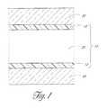
- FIG. 1is a schematic view of an integrated circuit transistor, including aluminum oxide or lanthanide oxide interfacial layers, in accordance with the preferred embodiments.
- FIG. 2is a flow chart of a preferred method of depositing aluminum oxide using an ALD process.
- FIG. 3is a flow chart illustrating a process of forming gate stacks, in accordance with a preferred embodiment of the invention.
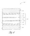
- FIG. 4is a schematic view of an integrated circuit capacitor comprising a nanolaminate structure, in accordance with the preferred embodiments.
- the present inventionutilizes a thin dielectric film as an interface layer between two materials to prevent a detrimental reaction between them.
- a detrimental reactionmay include a chemical reaction or diffusion.
- Al 2 O 3can be placed as a lower interface layer under any high-k material, or as a top interface layer that is compatible with polysilicon or SiGe (alloy of silicon and germanium).
- the primary example herein of such a dielectric interface filmis Al 2 O 3 ; however, as discussed below, lanthanide oxides have also been found to have excellent interfacial properties in a dielectric stack.
- Al 2 O 3 or lanthanide oxide thin filmsmay be used to prevent a solid phase from reacting with the surroundings.
- the solid phasecan be deposited directly over an Al 2 O 3 thin film.
- an Al 2 O 3 or lanthanide oxide layercan be deposited directly over the solid phase.
- the solid phasecan be sandwiched between two Al 2 O 3 or lanthanide oxide thin films.
- Al 2 O 3can act as a diffusion barrier interface and prevent the diffusion of molecules, atoms or ions from a solid phase on one side of the Al 2 O 3 layer to a solid phase on the other side of the Al 2 O 3 layer.
- Al 2 O 3may serve as a boron diffusion barrier.
- a diffusion barrier function of an interface layerat least one molecular monolayer of Al 2 O 3 is desired, preferably between about 1 and 4 monolayers, and more preferably between about 1 and 2 monolayers.
- the aluminum oxide interfacial layerpreferably has a thickness between about 3 ⁇ and 15 ⁇ , more preferably between about 3 ⁇ and 9 ⁇ .
- An Al 2 O 3 surfacecan also act as a nucleation layer at a top interface for further solid phase growth.
- a high dielectric materialcan be deposited on a lower aluminum oxide interface layer.
- An in situ doped silicon layer(such as boron-, arsenic- phosphorus- or germanium-doped silicon) can also be directly deposited directly over a top aluminum oxide interface layer on an Al 2 O 3 thin film in the production of a gate dielectric.
- the nucleation layerspeeds initial deposition of silicon-containing layers, particularly in situ doped silicon, which can have long nucleation times over SiO 2 , as is known in the art. Accordingly, throughput can be radically improved.
- nucleation layerAs little as one cycle of an ALD Al 2 O 3 process (representing less than one monolayer, typically about 1 ⁇ 3 of a monolayer) can improve nucleation times of deposition thereover, especially for the top aluminum oxide interface layer between a high-k material and a gate electrode. Such a partial monolayer will typically manifest as aluminum oxide “dots” evenly spread over the substrate. These separated dots are sufficient to provide rapid and uniform nucleation across the substrate. However, it is preferred for most integrated circuit contexts to produce an aluminum oxide layer thick enough to also serve as a barrier layer, as discussed in the previous paragraph.
- the inventionis particularly useful, therefore, in forming upper and/or lower interfaces on a high-k dielectric constant material, such as ZrO 2 .
- a high-k dielectric constant materialsuch as ZrO 2 .
- an Al 2 O 3 /ZrO 2 /Al 2 O 3 sandwich structurehas excellent physical and electrical properties in a gate dielectric.
- Lower equivalent oxide thickness (EOT)is obtained when Al 2 O 3 is used instead of SiO 2 as an interface layer, since the dielectric constant of Al 2 O 3 (on the order of 10) is higher than that of SiO 2 .
- High-k materialsinclude hafnium oxide (HfO 2 ), titanium dioxide (TiO 2 ), tantalum oxide (Ta 2 O 5 ), barium strontium titanate (BST), strontium titanate (ST), barium titanate (BT), lead zirconium titanate (PZT) and strontium bismuth tantalate (SBT). These materials and other, similar materials, while advantageously demonstrating high dielectric constants, tend to be unstable and/or inconsistent in composition, and also tend to require highly oxidizing environments during deposition.
- a lower aluminum oxide interface layeris preferably in the range of about 1-4 monolayers in thickness (representing about 3-15 ALD cycles with TMA and water), more preferably between about 1 monolayer and 2 monolayers.
- an Al 2 O 3 layercan prevent the agglomeration of a high-k material during the high-k deposition.
- an “ALD type process”designates a process in which deposition of vaporized material onto a surface is based on sequential and alternating self-saturating surface reactions.
- the principles of ALD type processeshave been presented by T. Suntola, e.g. in the Handbook of Crystal Growth 3, Thin Films and Epitaxy, Part B: Growth Mechanisms and Dynamics, Chapter 14, Atomic Layer Epitaxy, pp. 601-663, Elsevier Science B.V. 1994, the disclosure of which is incorporated herein by reference.
- reaction spacedesignates a reactor or reaction chamber in which the conditions can be adjusted so that deposition by ALD is possible.
- the present inventionprovides an oxide interface between two or more materials.
- one of the materialsis a high dielectric material, such as ZrO 2 .
- the high dielectric materialpreferably has a dielectric constant greater than 5. More preferably the high dielectric material has a dielectric constant greater than about 10.
- Such “high-k” materialsinclude oxides of Group 4 and Group 5 metals (e.g., Ti, Zr, Hf, V, Nb, Ta), as well as more complex oxides.
- “high-k” materialscan also include lanthanide oxides, such as lanthanum oxide (k ⁇ 21), neodymium oxide (k ⁇ 16) and cerium dioxide (k ⁇ 15).
- the present inventionprovides an aluminum oxide sandwich, wherein two aluminum oxide layers are used as interface layers separating three other materials.
- the structure of such an aluminum oxide sandwichcan be represented by material 1/Al 2 O 3 /material 2/Al 2 O 3 /material 3.
- materials 1 and 3are conductors in an integrated circuit, while material 2 is a thin dielectric film.
- Thinrefers to a dielectric layer thin enough to serve as a capacitor dielectric (in combination with the Al 2 O 3 interface layers) when charge is stored on one of the conductive materials 1 and 3.
- capacitor dielectric functionsare most typically found in gate dielectrics and memory cell dielectrics.
- an aluminum oxide or lanthanide oxide sandwich 15is part of a transistor gate electrode.
- FIG. 1depicts a cross section of such an arrangement.
- Aluminum oxide or lanthanide oxide layers 10 , 12directly contact either side of a dielectric material layer 20 .
- the oxide layers 10 , 12serve as interfacial layers between the dielectric material 20 and the overlying gate electrode 30 , and between the dielectric material and the underlying silicon substrate 40 .
- the gate electrodecomprises polycrystalline silicon, and more preferably poly-SiGe.
- the middle dielectric layeris preferably characterized by a high dielectric constant (high-k), comprising ZrO 2 in the illustrated embodiment.
- the high-k materialcan comprise multiple materials, either as a ternary structure or a laminate (see FIG. 4) of multiple high-k material layers.
- FIG. 3illustrates an exemplary sequence for forming interfacial layers in accordance with the preferred embodiments.
- the sequence shownis for forming a transistor gate dielectric structure between a semiconductor substrate and a gate electrode, including aluminum oxide interface layers sandwiching a high-k material.
- the semiconductor substrate surfacecan be optionally prepared 70 for subsequent deposition by ALD. Such preparation can include, for example, water or alcohol treatment, as described in more detail below.
- a first aluminum oxide interface layeris deposited 72 by ALD.
- a high-k layeris deposited 74 thereover. This layer can also be deposited in situ within the same reaction chamber.
- a second aluminum oxide interface layeris then deposited 76 by ALD over the high-k layer.
- a transistor gate electrodeis then deposited 78 over the second interface layer.
- a cluster tool having in situ wafer cleaning, ALD and CVD modulescan be employed, particularly where the interface layer is formed by ALD and the high-k material is formed by CVD or other method.
- alternating vapor-phase pulses of an aluminum or lanthanide source chemical and an oxygen source chemicalare fed to a reaction chamber having a reduced pressure and contacted with a heated substrate surface to form an aluminum or lanthanide oxide thin film.
- the source chemical pulsesare separated from each other by removal steps, preferably with flowing inert or noble gas, so that gas phase reactions are avoided and only self-saturating surface reactions are enabled.
- the general processwill be better understood by reference to FIG. 2, exemplifying aluminum oxide deposition by ALD, discussed below.
- the aluminum or lanthanide source chemicalis selected from a group of aluminum and lanthanide compounds that are volatile and thermally stable at the substrate temperature.
- Alkyl aluminum compoundshave at least one aluminum-carbon bond.
- source compoundsare trimethylaluminum (CH 3 ) 3 Al, triethylaluminum (CH 3 CH 2 ) 3 Al, tri-n-butylaluminum (n-C 4 H 9 ) 3 Al, diisobutylaluminum hydride (i-C 4 H 9 ) 2 AlH, diethylaluminum ethoxide (C 2 H 5 ) 2 AlOC 2 H 5 , ethylaluminum dichloride (C 2 H 5 ) 2 AlCl 2 , ethylaluminum sesquichloride (C 2 H 5 ) 3 Al 2 Cl 3 , diisobutylaluminum chloride (i-C 4 H 9 ) 2 AlCl and diethylaluminum iodide (C 2 H 5 ) 2 AlI. These compounds are commercially available from, e.g., Albemarle Corporation, USA.
- trimethylaluminum (CH 3 ) 3 Alis used as the aluminum source chemical.
- Aluminum alkoxidescontain an aluminum-oxygen-carbon (Al—O—C) bond.
- sources compoundsare aluminum ethoxide Al(OC 2 H 5 ) 3 , aluminum isopropoxide Al[OCH(CH 3 ) 2 ] 3 and aluminum s-butoxide Al(OC 4 H 9 ) 3 . These compounds are commercially available from, e.g., Strem Chemicals, Inc., USA.
- Aluminum beta-diketonateshave organic ligands coordinated to aluminum via oxygen atoms.
- Examples of source compoundsare aluminum acetylacetonate Al(CH 3 COCHCOCH 3 ) 3 , often shortened as Al(acac) 3 , and tris-(2,2,6,6-tetramethyl-3,5-heptanedionato)aluminum, usually shortened as Al(thd) 3 , Al(TMHD) 3 or Al(DPM) 3 .
- Volatile halogenated aluminum beta-diketonatesare also commercially available, such as aluminum hexafluoroacetylacetonate Al(CF 3 COCHCOCF 3 ) 3 , often shortened as Al(hfac) 3 . These compounds are commercially available from, e.g., Strem Chemicals, Inc., USA.
- Volatile, purely inorganic aluminum halidessuch as aluminum chloride AlCl 3 or Al 2 Cl 6 , aluminum bromide AlBr 3 , and aluminum iodide AlI 3 may be used as precursors
- anhydrous aluminum nitratecan be used as an aluminum source chemical for ALD.
- the synthesis of anhydrous Al(NO 3 ) 3has been described by G. N. Shirokova, S. Ya. Zhuk and V. Ya. Rosolovskii in Russian Journal of Inorganic Chemistry , vol. 21, 1976, pp. 799-802, the disclosure of which is incorporated herein by reference.
- the aluminum nitrate moleculebreaks into aluminum oxide when it is contacted with organic compounds, such as ethers.
- Lanthanidescan be made volatile with selected ligands that prevent interaction between lanthanide atoms in the precursor or source.
- Physically stable lanthanides from which to form these precursorsinclude scandium (Sc), yttrium (Y), lanthanum (La), cerium Ce, praseodymium (Pr), neodymium (Nd), samarium (Sm), europium (Eu), gadolinium (Gd), terbium (Tb), dysprosium (Dy), holmium (Ho), erbium (Er), thulium (Tm), ytterbium (Yb) and lutetium (Lu).
- Volatile or gaseous compounds that contain oxygen and are capable of reacting with an aluminum source compound on the substrate surface resulting in the deposition of aluminum oxideare used as oxygen source materials.
- the choice of oxygen source materialmay be influenced by the substrate on which the aluminum oxide layer is to be deposited and thus whether the aluminum oxide thin film will form a top interface layer or a bottom interface layer.
- hydrogen peroxide, ozone and oxygen with unpaired electronsare preferably used only for the top interface.
- Water and alcoholssuch as methanol, ethanol and isopropanol, may be used for any interface, as they are less liable to oxidize the underlying silicon during the deposition process. Alcohols are especially reactive with aluminum halides.
- a substrateis loaded into a reaction space.
- the reaction spaceis adjusted to the desired temperature and the gas atmosphere of the reaction space is adjusted to the desired pressure.
- a repeatable process sequence including four basic steps, as depicted in FIG. 2,is begun.
- Aluminum oxide depositionis shown, though the skilled artisan will appreciate, in view of the present disclosure, that a similar process can be used to deposit lanthanide oxides.
- a vapor phase pulse 50 of an aluminum source chemicalis introduced into the reaction space and contacted with the substrate surface.
- the surplus aluminum source chemical and any possible reaction byproductsare removed 55 from the reaction space by varying the reaction space pressure and/or by inert gas flow.
- a vapor phase pulse 60 of an oxygen sourceis introduced into the reaction chamber and contacted with the substrate surface.
- the surplus oxygen source chemical and any possible reaction byproductsare removed 65 from the reaction space by varying the reaction space pressure and/or by inert gas flow.
- the illustrated process cycleis repeated until an aluminum oxide thin film of a desired thickness is obtained.
- the substrate having the thin filmis unloaded from the reaction chamber or another thin film process is started.
- substrate surfacesmay benefit from a surface pretreatment 70 prior to ALD thereover.
- a few exemplary surface preparation treatmentsare provided below, depending upon the starting surface.
- Substrates with native oxidewill typically not require surface preparation. Rather, the above-described ALD process (e.g., with the TMA/purge/water/purge cycle of Example 1 below) will initially react with the native oxide and deposition will proceed as discussed above.
- ALD processe.g., with the TMA/purge/water/purge cycle of Example 1 below
- a first water pulsemay react with the silicon surface and leave a hydroxyl terminated (—OH) or oxygen bridged (Si—O—Si) silicon surface that serves as a starting surface for the chemisorption of aluminum alkyls.
- —OHhydroxyl terminated
- Si—O—Sioxygen bridged
- Ozonereacts with silicon and thus forms a silicon dioxide layer or increases the thickness of the native silicon dioxide layer, depending of course upon temperature, exposure duration and O 3 concentration.
- Either a native oxide or H-terminated silicon surfacecan be thus prepared for the formation of an aluminum oxide thin film with an initial ozone pulse.
- a silicon dioxide surface(preferably a very thin native oxide) can be treated with an aluminum source chemical to produce an exchange reaction with the surface, replacing SiO 2 with Al 2 O 3 .
- an aluminum source chemicalfor example:
- Lis a ligand, preferably a halide such as chloride, bromide or iodide, more preferably comprising chloride, as set forth in Example 3 below.
- the Gibb's free energiescan be calculated, e.g., with HSC Chemistry, Ver. 4.1, Outokumpu Research Oy, Pori, Finland.
- the exchange reactionis preferably applied to relatively thin layers.
- the aluminum oxide layer formed by the exchange reactionis used as an interface layer between silicon and a high-k material
- Amorphous aluminum and lanthanide oxides deposited by ALDare utilized in dielectric thin films. These oxides are combined with high-k materials to produce state-of-the-art gate dielectrics and integrated circuit capacitor dielectrics, particularly for integrated memory cells.
- Exemplary transistorsinclude silicon or SiGe gate electrodes, and monocrystalline silicon or GaAs substrates.
- Exemplary memory devicesinclude dynamic random access memory (DRAM), synchronous DRAM (SDRAM), direct RambusTM DRAM (DRDRAM), static random access memory (SRAM), and non-volatile memory devices.
- DRAMdynamic random access memory
- SDRAMsynchronous DRAM
- DRAMdirect RambusTM DRAM
- SRAMstatic random access memory
- Non-volatile memory devicesinclude read only memory (ROM), programmable ROM (PROM), erasable programmable ROM (EPROM), electrically erasable programmable ROM (EEPROM) and flash memory devices.
- the lanthanide elementssuch as lanthanum (La), yttrium (Y) and scandium (Sc), have also been known as rare earth elements.
- the use of the word “rare” in this termis misleading because these elements are not particularly rare on Earth.
- cerium (Ce)is 5 times as abundant as lead (Pb).
- Even thulium (Tm)the rarest of the stable rare earth elements, is more abundant than iodium (I).
- Lanthanidesare usually extracted either from monazite or bastnaesite minerals.
- “physically stable lanthanides”are defined as scandium (Sc), yttrium (Y), lanthanum (La), cerium Ce, praseodymium (Pr), neodymium (Nd), samarium (Sm), europium (Eu), gadolinium (Gd), terbium (Tb), dysprosium (Dy), holmium (Ho), erbium (Er), thulium (Tm), ytterbium (Yb) and lutetium (Lu).
- Lanthanide compoundsare similar to compounds of aluminum in certain aspects.
- Aluminum oxide Al 2 O 3has a very high melting point (2070° C.), while the melting point of yttrium oxide Y 2 O 3 is 2410° C. and that of lanthanum oxide La 2 O 3 2307° C. All of these oxides are also quite inert and have high resistivities. Bonds between the metal and oxygen atoms are very strong. For example, Al—O has a bond strength of 512 kJ/mol, La—O has a bond strength of 799 kJ/mol and Y—O has a bond strength of 715 kJ/mol. CRC HANDBOOK OF CHEMISTRY AND PHYSICS, CRC Press, Inc.
- High melting points and bond strengthsindicate that amorphous aluminum and lanthanide oxides can be heated to high temperatures without crystallization. Chemical inertness is beneficial for keeping nanolaminate layers (as described below) separated from each other and from surrounding materials and having a stable dielectric structure during the fabrication and lifetime of the manufactured devices.
- Nanolaminate dielectric structureshave been reported in the past.
- Ritala et al.have made Al 2 O 3 —TiO 2 nanolaminates by ALD using TiCl 4 , AlCl 3 , H 2 O as source chemicals, where the TiO 2 layers were polycrystalline and the Al 2 O 3 layers were amorphous.
- M. RitalaM. Leskela, L. Niinisto, T. Prohaska, G. Friedbacher and M. Grassenbauer, “Surface roughness reduction in atomic layer epitaxy growth of titanium dioxide thin films,” Thin Solid Films , Vol. 249 (1994), pp. 155-162.
- Al 2 O 3 layers placed in the filmreduced the surface roughness of the TiO 2 thin film.
- Ta 2 O 5 —Al 2 O 3 nanolaminatesare also disclosed in H. Kattelus, M. Ylilammi, J. Saarilahti, J. Antson and S. Lindfors, “Layered Tantalum-Aluminum Oxide Films Deposited by Atomic Layer Epitaxy,” Thin Solid Fihns , Vol. 225 (1993), pp. 296-298.
- TaCl 5 , AlCl 3 and H 2 Owere used as source chemicals. With depositions conducted at 300° C. and no post-deposition treatment, the authors conclude that even small amounts of aluminum oxide introduced as thin layers in the tantalum oxide results in improvement in the dielectric properties.
- a nanolaminateconsists of alternating crystalline and amorphous layers of metal oxides. Amorphous layers decrease the leakage current through the nanolaminate while crystalline layers can increase the dielectric constant of the whole nanolaminate structure. According to another embodiment of the present invention, the nanolaminate contains only amorphous metal oxide layers for obtaining extremely low leakage current while having sufficiently high dielectric constant.
- High-k materialfor the purposes of describing layers in the nanolaminate structure of the present embodiment, is defined as a metal oxide that has higher dielectric constant than Al 2 O 3 (about 10).
- High-k metal oxides that can be utilized in the metal oxide nanolaminateinclude oxides of elements in Group 4, (Ti, Zr and Hf) and Group 5 (V, Nb and Ta) of the periodic table of elements.
- “High-k” materialscan also include lanthanide oxides, such as lanthanum oxide (k ⁇ 21, neodymium oxide (k ⁇ 16) and cerium dioxide (k ⁇ 15).
- amorphous layerssuch as Al 2 O 3 and lanthanide oxides
- Such “leaky” materialscan include binary compounds, (e.g., SnO 2 , WO 3 ), ternary compounds (e.g., metal titanates such as Ba, Sr, Ca, Mg or Pb titanates; metal zirconates such as PbZrO 3 ; and metal niobates such as Pb 5 Nb 4 O 15 ) and quaternary compounds (e.g., Ba—Zn—Ta—oxide and Zr—Sn—Ti oxide).
- binary compoundse.g., SnO 2 , WO 3
- ternary compoundse.g., metal titanates such as Ba, Sr, Ca, Mg or Pb titanates; metal zirconates such as PbZrO 3 ; and metal niobates such as Pb 5 Nb 4 O 15
- quaternary compoundse.g., Ba—Zn—Ta—oxide
- the crystal growth of a high-k metal oxidecan be interrupted with an intermediate amorphous metal oxide layer, particularly Al 2 O 3 or a lanthanide oxide, in a stack of dielectric layers (a dielectric “nanolaminate”).
- These intermediate amorphous layersaffect the crystallization temperature of the dielectric material. Decreasing the individual metal oxide layer thickness in the nanolaminate structure, while keeping the total thickness of the nanolaminate unchanged, increases the crystallization temperature of the high-k metal oxide. Increased crystallization temperature can effectively decrease the leakage current through the dielectric material, since an amorphous thin film will demonstrate a lower leakage current than a corresponding crystalline thin film.
- the most basic nanolaminate constructioncomprises at least two high-k layers separated by a thin aluminum oxide or lanthanide oxide film, thereby interrupting the crystal structure of the high-k layers.
- the separating oxide filmhas a thickness of no more than about 4 molecular monolayers, more preferably no more than about 2 molecular monolayers, thereby minimizing the thickness of the dielectric nanolaminate while still accomplishing the interruption of high-k crystal structure.
- the separating oxide filmhas a thickness between about 3 ⁇ and 15 ⁇ , more preferably less than about 10 ⁇ .
- This interrupting or separating layeris also referred to herein as an interface layer, particularly an “intermediate” interface layer.
- the stackfurther includes additional aluminum oxide or lanthanide oxide films on the outer surfaces of the high-k dielectric layers.
- a memory cell structure 100including 4 thin interface films alternated with 3 high-k films.
- a dielectric nanolaminate 110comprises three 30 ⁇ high-k films 112 of ZrO 2 , separated by 5 ⁇ intermediate interface films 113 of Al 2 O 3 .
- the outer surfaces of the outermost high-k films 112are covered with 10 ⁇ outer interface films 114 of Al 2 O 3 .
- the outermost aluminum oxide filmsare twice the thickness of the intermediate aluminum oxide films.
- the aluminum oxide films 113 , 114can be replaced with lanthanide oxide film.
- the zirconium oxide films 112can be replace by lanthanide oxides.
- ALD Al 2 O 3 and ALD lanthanide oxidescan perfectly cover the substrate surface, even when the oxide layer thickness approaches the lattice constant of the metal oxide. Most of the dielectric thickness can be reserved for the high-k component. Thus, the capacitance density of the layered dielectric structure made by ALD is better than that obtained with other deposition methods.
- IC capacitor applicationssuch as DRAM memory cell capacitors, will benefit from the present invention.
- the gate oxide thicknesscan be minimized without sacrificing the reliability of the manufactured devices.
- EOTequivalent oxide thickness
- dielectric structures layers with low EOT yet low leakage currentis beneficial in that it facilitates scaling transistor and integrated circuit designs generally.
- forming a metal oxide nanolaminate by ALDproduces excellent EOT with low leakage current.
- Atomic layer deposition (ALD) processesrequire volatile source chemicals that are thermally stable and reactive at the deposition temperature.
- Sufficient volatility for purposes of ALDis defined as a minimum vapor pressure of the compound that is sufficient to cover the whole substrate with a single molecular layer of source chemical molecules during the source pulse time at the deposition temperature.
- the minimum vapor pressure of the source compoundshould be approximately 0.02 mbar at the deposition temperature.
- the deposition temperatureis selected to be above condensation temperature while below thermal decomposition temperatures for the selected precursors, enabling adsorption without decomposition and permitting the self-limiting process.
- lanthanidescan be made volatile with selected ligands that prevent interaction between lanthanide atoms in the precursor or source.
- Aluminumhas a wide range of volatile compounds, such as halides AlCl 3 , AlBr 3 , AlI 3 , alkoxides, such as Al(OCH 2 CH 3 ) 3 , alkyls, such as (CH 3 ) 3 Al, beta-diketonates, such as Al(thd) 3 and anhydrous nitrate Al(NO 3 ) 3.
- volatile compoundssuch as halides AlCl 3 , AlBr 3 , AlI 3 , alkoxides, such as Al(OCH 2 CH 3 ) 3 , alkyls, such as (CH 3 ) 3 Al, beta-diketonates, such as Al(thd) 3 and anhydrous nitrate Al(NO 3 ) 3.
- the metal oxide nanolaminatescan also be grown by ALD at a different pressure range.
- Other possible deposition methods at very low pressurese.g., molecular beam epitaxy (MBE), can be used for growing the metal oxide nanolaminate.
- MBEmolecular beam epitaxy
- the aluminum source pulse 50comprises trimethyl aluminum or TMA) ((CH 3 ) 3 Al) fed into the reaction space. TMA chemisorbs on hydroxyl (—OH) groups on the substrate surface. Methane is released as a byproduct.
- the self-saturating surface reactionleaves a methyl-terminated aluminum oxide layer on the surface.
- the removal 55comprises flowing inert gas flow to purge residual TMA and methane from the reaction space.
- the oxygen source pulse 60comprises a water pulse that reacts with the methyl groups on aluminum oxide.
- the self-saturating surface reactionleaves a hydroxyl-terminated aluminum oxide layer on the substrate surface and methane gas is released as a byproduct.
- the second removal 65also comprises flowing inert gas to purge residual water and methane from the reaction space.
- the substrate surfaceis now ready to receive the next TMA pulse. Alternating TMA and H 2 O reactant pulses increases the thickness of the aluminum oxide film uniformly over the substrate until a desired thickness is obtained.
- a silicon waferwas loaded into the reaction space of PulsarTM 2000 reactor (commercially available from ASM Microchemistry of Espoo, Finland), which is designed for ALD processes.
- the reaction spacewas evacuated to vacuum with a mechanical vacuum pump. After evacuation the pressure of the reaction space was adjusted to about 5-10 mbar (absolute) with flowing nitrogen gas that had a purity of 99.9999%. Then the reaction space was stabilized at 300° C. Alternating vapor phase pulses of (CH 3 ) 3 Al and H 2 O, vaporized from external sources, were introduced into the reaction space and contacted with the substrate surface. The source chemical pulses were separated from each other with flowing nitrogen gas.
- the pulsing cycleconsisted of four basic steps:
- Each of the pulsing and purging timeswas on the order of 0.5 s.
- the pulsing cyclewas repeated 100 times.
- the silicon substratewas unloaded from the reaction space.
- the growth rate of Al 2 O 3 from (CH 3 ) 3 Al and H 2 Owas typically near 0.1 nm/cycle at 300° C.
- the number of cyclesdetermine the thickness of the layer, with an average of about 1 ⁇ /cycle, or about 3-4 cycles/monolayer (Al 2 O 3 has a bulk lattice parameter of about 3 ⁇ ).
- the methyl terminations left by each TMA pulsereduce the number of available chemisorption sites, such that less than a full monolayer forms with each pulse.
- preferably between 1 and 18 cycles, more preferably between about 3 and 12 cycles, and most preferably between about 3 and 8 cyclesare performed.
- the Al 2 O 3 layermay serve as an oxygen diffusion barrier and thus prevent the oxidation of the silicon substrate.
- the Al 2 O 3 layerserves as a seed layer for further thin film growth.
- a high-k layermay be grown on the Al 2 O 3 layer.
- silicon or silicon germaniumis deposited on the Al 2 O 3 layer, and the Al 2 O 3 layer serves as an interfacial layer.
- Aluminum acetylacetonatei.e. Al(acac) 3
- tris-(2,2,6,6-tetramethyl-3,5-heptanedionato)aluminumi.e. Al(thd) 3
- aluminum oxideis formed and Hacac or Hthd vapor is released.
- ozoneis preferably used only for the growth of the top interfacial aluminum oxide layer, as noted above in the discussion of preferred oxygen source materials, to avoid oxidation of the underlying substrate.
- An ALD reactor or a CVD reactoris used for the process.
- a substrate with a silicon dioxide surfaceis placed into the reaction space.
- the pressurecan be atmospheric, but preferably the pressure of the reaction space is adjusted to about 1-10 mbar.
- the substrate temperatureis adjusted to between about 300° C. and 400° C.
- Vaporized aluminum compound, preferably aluminum halide and more preferably aluminum chloride,is contacted with the substrate surface for about two minutes.
- the completion of the exchange reactioncan be monitored, e.g. with a quadrupole mass spectrometer located at the exhaust side of the reaction space.
- the reactionhas ended when there is no volatile silicon compound (e.g., silicon chloride) left in the gas phase of the reaction space.
- the flow of the volatile aluminum compound into the reaction spaceis stopped.
- the reaction spaceis preferably evacuated to remove residual gaseous aluminum compound before unloading the substrate or continuing with another thin film process.
- the replacement reactiondepends upon diffusion of the aluminum source chemical through the growing aluminum oxide layer, which forms first at the surface. Accordingly, the process is self-limiting and desirably is conducted to form only a thin interfacial aluminum oxide layer, with thicknesses in the ranges discussed above. For purposes of improved nucleation thereover, the thickness can be less than a full monolayer.
- a SiO 2 gate dielectric layercan be formed over a substrate and only a thin top portion of the SiO 2 is converted, serving as a nucleation layer for later polysilicon or poly-SiGe gate electrode deposition, and preferably also as a diffusion barrier.
- the aluminum oxide interface layerhas an increased k value as compared to the prior SiO 2 surface.
- a thin SiO 2 layeris completely converted into a thin interfacial aluminum oxide in contact with the underlying substrate.
- the gate dielectriccan be completed by deposition of a high-k material over the aluminum oxide interface layer, and optionally a further top interface layer of aluminum oxide.
- a silicon waferwas loaded into the reaction space of PulsarTM 2000 reactor (ASM Microchemistry), which is designed for ALD processes.
- the reaction spacewas evacuated to vacuum with a mechanical vacuum pump. After evacuation the pressure of the reaction space was adjusted to about 5-10 mbar (absolute) with flowing nitrogen gas that had a purity of 99.9999%. Then the reaction space was stabilized at about 300° C.
- the pulsing cycleconsisted of the four basic steps:
- Each of the pulsing and purging timeswas in the order of 0.5 s.
- the pulsing cyclewas repeated 3, 6, 9 or 12 times, representing about 1, 2, 3 and 4 monolayers, respectively.
- a high-k layerwas formed on the Al 2 O 3 surface.
- the high-k layersuch as HfO 2 or ZrO 2
- the lower thickness limit for the Al 2 O 3 layer that separates the silicon substrate from the high-k materialis about one molecular layer to serve as a minimal thickness barrier layer against oxygen and other diffusion (e.g., boron diffusion).
- oxygen and other diffusione.g., boron diffusion.
- This single-cycle processrepresents less than a full monolayer, due to the physical size of the chemisorbed species (including organic tails) from the first pulse.
- the upper thickness limit for the Al 2 O 3 layerdepends on the acceptable equivalent oxide thickness (EOT).
- a silicon waferwas dipped in HF solution to remove silicon dioxide. Residual HF was washed away with purified water. Then the wafer was placed in the reaction chamber of an F450TM reactor, which is commercially available from ASM Microchemistry Ltd. of Espoo, Finland.
- Reactor conditionswere set for sequential deposition of both aluminum oxide and zirconium oxide films by ALD.
- the reactorwas evacuated with a mechanical pump.
- the pressure of the reaction chamberwas adjusted in the 5-10 mbar range with flowing nitrogen gas.
- the temperature of the reaction chamber, and thus of the substrate,was set to about 300° C.
- ZrCl 4 source chemical outside the reaction chamberwas heated to 175° C.-180° C.
- Trimethyl aluminum TMAwas vaporized at room temperature from an external source container.
- H 2 Owas used as an oxygen source. It was vaporized at room temperature from an external source container.
- Any inactive gas, such as nitrogen or argon,can be used for purging the reactor. Nitrogen was used for the experiments.
- the depositionstarted with the growth of an Al 2 O 3 layer.
- An aluminum oxide thin filmcan be prepared on a silicon substrate as described above.
- a slightly modified processwas employed in the experiments.
- TMA vaporwas introduced to the reaction chamber and contacted with the wafer surface for 0.2 s. This is referred to as pulse 1.
- the reaction chamberwas purged with nitrogen gas for 1.1 s to remove surplus TMA and byproducts from the reaction chamber. This is referred to as purge 1.
- water vaporwas introduced to the reaction chamber and exposed to the wafer surface for 1.5 s. This is referred to as pulse 2.
- Residual H 2 O and reaction byproductswere removed by purging the reaction chamber for 3.0 s. This is referred to as purge 2.
- the reactantsare supplied in sufficient quantity for the given other parameters to saturate the surface.
- This deposition cycleconsisting of pulse 1 , purge 1 , pulse 2 and purge 2 , was repeated 10 times.
- the deposition rate of Al 2 O 3 from TMA and H 2 Ois about 1 ⁇ /cycle on average at 300° C., such that the Al 2 O 3 layer thickness after 10 cycles is about 10 ⁇ .
- a high-k dielectric layeris then formed on the aluminum oxide thin film.
- the high-k dielectric layermay be made of any material known in the art.
- the dielectric constantis greater than 5, more preferably greater than 10.
- the high-k dielectric layercan also be formed by an ALD type process.
- the high-k dielectric materialcan be formed by any suitable method (e.g., MOCVD), and the advantages of the described aluminum oxide interface layers will still obtain.
- ZrO 2is deposited by an ALD type process.
- ZrCl 4 vaporwas introduced to the reaction chamber and exposed the wafer surface for 1.5 s. This is referred to as pulse A.
- the reaction chamberwas purged with nitrogen gas for 3.0 s to remove surplus ZrCl 4 and byproducts from the reaction chamber. This is referred to as purge A.
- purge AThen water vapor was introduced to the reaction chamber and exposed to the wafer surface for 3.0 s.
- pulse BResidual H 2 O and reaction byproducts were removed by purging the reaction chamber for 4.0 s. This is referred to as purge B.
- purge BResidual H 2 O and reaction byproducts were removed by purging the reaction chamber for 4.0 s. This is referred to as purge B.
- the reactantsare supplied in sufficient quantity for the given other parameters to saturate the surface.
- the cycle of Table Iconsisting of pulse A, purge A, pulse B, purge B, was repeated 51 times.
- the average deposition rateis about 0.59 ⁇ /cycle at 300° C., such that the ZrO 2 thickness was about 30 ⁇ .
- temperatures during the ZrO 2 depositionwere kept at the same temperature as the previous Al 2 O 3 deposition to facilitate rapid in situ processing. More generally, temperatures during the process preferably fall between about 200° C. and 500° C.
- the temperatureis more preferably at the low end of this range, between about 200° C. and 250° C., and most preferably at about 225° C.
- the temperatureis more preferably at the high end of this range, between about 250° C. and 500° C., and most preferably about 300° C.
- mixtures of amorphous and crystalline compositionresult at the boundary of these two regimes.
- the illustrated processproduces a largely crystalline ZrO 2 film.
- the metal monolayer formed in the metal phaseis self-terminated with chloride, which does not readily react with excess ZrCl 4 under the preferred conditions.
- the preferred oxygen source gasreacts with the chloride-terminated surface during the oxygen phase in a ligand-exchange reaction limited by the supply of zirconium chloride complexes previously adsorbed. Moreover, oxidation leaves a hydroxyl and oxygen bridge termination that does not further react with excess oxidant in the saturative phase.
- sufficient cyclesare conducted to grow between about 20 ⁇ and 60 ⁇ of ZrO 2 . More preferably, sufficient cycles are conducted to grow between about 20 ⁇ and 40 ⁇ .
- the dielectric constant of the layeris between about 18 and 24. In the illustrated examples, 30 ⁇ of ZrO 2 was formed.
- a second layer of aluminum oxideis deposited on top of the high-k layer, in this case ZrO 2 , also by the ALD Al 2 O 3 process described above and summarized in Table I.
- the structurewas coated with another 10 ⁇ of aluminum oxide.
- the dielectric sandwichcomprised 10 ⁇ Al 2 O 3 /30 ⁇ ZrO 2 /10 ⁇ Al 2 O 3 .
- the second layer of aluminum oxideserves as a nucleation layer for subsequent deposition of a polysilicon or poly-SiGe gate electrode layer, and more preferably also serves as a minimum thickness to serve as a diffusion barrier between the high-k material and a second material.
- the remaining components of a gate stackare formed on the upper layer of aluminum oxide by methods well known in the art.
- known CVD processes for depositing doped silicon and poly-SiGe layersnucleate rapidly on Al 2 O 3 , improving overall throughput.
- the aluminum oxide layers present between the substrate and the high-k material and between the high-k material and the gate electrodeact as diffusion barriers and allow the gate dielectric to function properly.
- the aluminum oxide layershelp to stabilize the high-k material, allowing for a repeatable, production worthy process of manufacturing gate electrodes in integrated circuits.
- source chemical combinationsdepends on the location of the interface. When depositing an interface layer on silicon by ALD, highly oxidative source chemicals should be avoided. It is preferable to use a relatively mild oxygen source such as water. Water reacts quickly with alkyl aluminum compounds but does not oxidize silicon, especially when the substrate temperature is below 300° C.
- mild oxygen sourcesas well as highly oxidative source chemicals (e.g., ozone) can be used.
- highly oxidative source chemicalse.g., ozone
- the deposition of the Al 2 O 3 interface layeris not limited to the ALD method.
- Example 3provides a different but also self-limiting process for thin aluminum oxide layer formation.
- other CVD, MOCVD or PVD methodscan be applied as long as a sufficiently uniform film covering the substrate is obtained.
Landscapes
- Chemical & Material Sciences (AREA)
- Engineering & Computer Science (AREA)
- Organic Chemistry (AREA)
- General Chemical & Material Sciences (AREA)
- Chemical Kinetics & Catalysis (AREA)
- Materials Engineering (AREA)
- Mechanical Engineering (AREA)
- Metallurgy (AREA)
- Condensed Matter Physics & Semiconductors (AREA)
- Physics & Mathematics (AREA)
- Inorganic Chemistry (AREA)
- General Physics & Mathematics (AREA)
- Manufacturing & Machinery (AREA)
- Computer Hardware Design (AREA)
- Microelectronics & Electronic Packaging (AREA)
- Power Engineering (AREA)
- Formation Of Insulating Films (AREA)
- Semiconductor Memories (AREA)
- Insulated Gate Type Field-Effect Transistor (AREA)
- Chemical Vapour Deposition (AREA)
- Semiconductor Integrated Circuits (AREA)
Abstract
Description
The present application claims the priority benefit under 35 U.S.C. §119(e) to prior provisional application No. 60/239,040, filed Oct. 10, 2000, entitled METHOD OF DEPOSITING OXIDE THIN FILMS, provisional application No. 60/244,789, filed Oct. 31, 2000, entitled ALUMINUM OXIDE INTERFACE FILMS AND METHODS THEREFOR, and provisional application No. 60/247,115, filed Nov. 10, 2000, entitled DIELECTRIC INTERFACE FILMS AND METHODS THEREFOR.
The present invention relates generally to thin dielectric films in integrated circuits, and more particularly to interface layers for dielectric thin films.
Atomic Layer Deposition (ALD) is a self-limiting process, whereby alternated pulses of reaction precursors saturate a substrate and leave no more than one monolayer of material per pulse. The precursors and deposition conditions are selected to ensure self-saturating reactions. For example, an adsorbed layer in one pulse leaves a surface termination that is non-reactive with the gas phase reactants of the same pulse. A subsequent pulse of different reactants do react with the previous termination to enable continued deposition. Thus, each cycle of alternated pulses leaves no more than about one molecular layer of the desired material. The principles of ALD type processes have been presented by T. Suntola, e.g. in the Handbook of Crystal Growth 3, Thin Films and Epitaxy, Part B: Growth Mechanisms and Dynamics, Chapter 14, Atomic Layer Epitaxy, pp. 601-663, Elsevier Science B.V. 1994.
Recently, these processes have been suggested for use in semiconductor fabrication. However, due to the slowness of the process (depositing one atomic layer of material per cycle), ALD has been of little practical benefit for current commercial process flows.
One material for which ALD processes have been developed is aluminum oxide (Al2O3). The deposition of aluminum oxide by ALD type processes is well known in the art. See, e.g., E.-L. Lakomaa, A. Root, T. Suntola, “Surface reactions in Al2O3growth from trimethylaluminium and water by atomic layer epitaxy”, Appl. Surf. Sci. 107 (1996) 107-115. This article is incorporated herein by reference.
In accordance with one aspect of the invention, an oxide interface layer is provided for a dielectric structure positioned between two conductive materials in an integrated circuit. The preferred embodiments employ metal oxide thin films for the interface layer, particularly aluminum oxide and lanthanide (“rare earth”) oxides, which can advantageously remain amorphous even after exposure to high temperatures. The oxide interface layer is preferably deposited by an atomic layer deposition (ALD) type process. Advantageously, the preferred interface materials do not readily react with many other materials and are very good barriers against the diffusion of molecules, atoms and ions. Al2O3and lanthanide oxides can be deposited by ALD processes with excellent control; extremely thin, uniformly thick layers can be formed without pinholes and at a wide range of substrate temperatures, depending on the source chemicals. Thus, ALD enables oxide layers thin enough to serve as an interface layer without adversely affecting electrical properties of the integrated circuit.
In accordance with another aspect of the invention, a high dielectric constant (high-k) dielectric structure is provided in an integrated circuit. The high-k dielectric structure comprises a first interfacial layer of aluminum oxide, a layer of high-k material directly adjacent the first interfacial layer, and a second interfacial layer of aluminum oxide directly adjacent the high-k material. The high-k material preferably has a dielectric constant of at least about 5, and more preferably at least about 10. Exemplary high-k materials include, but are not limited to, zirconium oxide (ZrO2), hafnium oxide (HfO2), titanium oxide (TiO2), tantalum oxide (Ta2O5), barium strontium titanate (BST), strontium titanate (ST), barium titanate (BT), lead zirconium titanate (PZT), lead strontium titanate (PST), strontium bismuth tantalate (SBT), metal silicates, aluminum nitride and nitrided metal oxides (e.g., TaxOyNbz, NbxOyNz). The aluminum oxide interfacial layers can also be replaced by lanthanide oxide layers.
The dielectric structure is positioned between a first conductor and a second conductor. Aluminum oxide and lanthanide oxides have been found particularly beneficial as interface layers between doped semiconductor structures, such as a doped silicon substrate in a transistor structure, and other dielectric materials. Furthermore, their excellent interfacial properties facilitate advanced materials. For example, aluminum oxide has been found particularly advantageous between high-k materials and poly-SiGe gate electrodes. During CVD of SiGe, nucleation over ALD Al2O3during initial phases of deposition was found superior to that over SiO2, thus speeding overall deposition rates. Other gate electrode materials may also be made possible due to superior nucleation of depositions thereover and protection against corrosion and impurity diffusion offered by the aluminum oxide interface between the gate electrode and the high-k material. In another example, a high-k dielectric structure (including a high-k material sandwiched between aluminum or lanthanide oxide interfacial layers) serves as a capacitor dielectric in an integrated circuit. The interfacial layers are of particular utility over silicon electrodes, such as hemispherical grained silicon (HSG-Si), but are also useful barriers for protection of other oxidation-susceptible electrode materials.
Another aspect of the present invention is an aluminum oxide layer or a lanthanide oxide layer located between two materials, where the oxide layer has a thickness between one full molecular monolayer and about 4 molecular monolayers. The oxide layer prevents diffusion of molecules from one material to the other.
Another aspect of the invention provides a method of preventing the oxidation of a substrate by depositing a layer of aluminum oxide or lanthanide oxide on the substrate by an ALD type process. Substrates otherwise susceptible to oxidation include conventional semiconductor substrates, such as single-crystal silicon wafers or epitaxial layers.
These and other aspects of the invention will be readily understood in view of the description below and the appended drawings, which are meant to illustrate and not to limit the invention, and in which:
FIG. 1 is a schematic view of an integrated circuit transistor, including aluminum oxide or lanthanide oxide interfacial layers, in accordance with the preferred embodiments.
FIG. 2 is a flow chart of a preferred method of depositing aluminum oxide using an ALD process.
FIG. 3 is a flow chart illustrating a process of forming gate stacks, in accordance with a preferred embodiment of the invention.
FIG. 4 is a schematic view of an integrated circuit capacitor comprising a nanolaminate structure, in accordance with the preferred embodiments.
While illustrated in the context of transistor gate stacks, the skilled artisan will readily find application for the principles and advantages disclosed herein to other situations where similar electrical and physical properties at an interface are desired.
The present invention utilizes a thin dielectric film as an interface layer between two materials to prevent a detrimental reaction between them. A detrimental reaction may include a chemical reaction or diffusion. For example, Al2O3can be placed as a lower interface layer under any high-k material, or as a top interface layer that is compatible with polysilicon or SiGe (alloy of silicon and germanium). The primary example herein of such a dielectric interface film is Al2O3; however, as discussed below, lanthanide oxides have also been found to have excellent interfacial properties in a dielectric stack.
Al2O3or lanthanide oxide thin films may be used to prevent a solid phase from reacting with the surroundings. For example, the solid phase can be deposited directly over an Al2O3thin film. Alternatively an Al2O3or lanthanide oxide layer can be deposited directly over the solid phase. In a third variation, the solid phase can be sandwiched between two Al2O3or lanthanide oxide thin films.
More particularly, Al2O3can act as a diffusion barrier interface and prevent the diffusion of molecules, atoms or ions from a solid phase on one side of the Al2O3layer to a solid phase on the other side of the Al2O3layer. For example, Al2O3may serve as a boron diffusion barrier. For a diffusion barrier function of an interface layer, at least one molecular monolayer of Al2O3is desired, preferably between about 1 and 4 monolayers, and more preferably between about 1 and 2 monolayers. In terms of absolute thickness, the aluminum oxide interfacial layer preferably has a thickness between about 3 Å and 15 Å, more preferably between about 3 Å and 9 Å.
An Al2O3surface can also act as a nucleation layer at a top interface for further solid phase growth. In the context of integrated circuit formation, a high dielectric material can be deposited on a lower aluminum oxide interface layer. An in situ doped silicon layer (such as boron-, arsenic- phosphorus- or germanium-doped silicon) can also be directly deposited directly over a top aluminum oxide interface layer on an Al2O3thin film in the production of a gate dielectric. The nucleation layer speeds initial deposition of silicon-containing layers, particularly in situ doped silicon, which can have long nucleation times over SiO2, as is known in the art. Accordingly, throughput can be radically improved. To serve as a nucleation layer, as little as one cycle of an ALD Al2O3process (representing less than one monolayer, typically about ⅓ of a monolayer) can improve nucleation times of deposition thereover, especially for the top aluminum oxide interface layer between a high-k material and a gate electrode. Such a partial monolayer will typically manifest as aluminum oxide “dots” evenly spread over the substrate. These separated dots are sufficient to provide rapid and uniform nucleation across the substrate. However, it is preferred for most integrated circuit contexts to produce an aluminum oxide layer thick enough to also serve as a barrier layer, as discussed in the previous paragraph.
The invention is particularly useful, therefore, in forming upper and/or lower interfaces on a high-k dielectric constant material, such as ZrO2. For example, an Al2O3/ZrO2/Al2O3sandwich structure has excellent physical and electrical properties in a gate dielectric. Lower equivalent oxide thickness (EOT) is obtained when Al2O3is used instead of SiO2as an interface layer, since the dielectric constant of Al2O3(on the order of 10) is higher than that of SiO2. Other high-k materials include hafnium oxide (HfO2), titanium dioxide (TiO2), tantalum oxide (Ta2O5), barium strontium titanate (BST), strontium titanate (ST), barium titanate (BT), lead zirconium titanate (PZT) and strontium bismuth tantalate (SBT). These materials and other, similar materials, while advantageously demonstrating high dielectric constants, tend to be unstable and/or inconsistent in composition, and also tend to require highly oxidizing environments during deposition. Thus, to prevent oxidation of the underlying substrate, a lower aluminum oxide interface layer is preferably in the range of about 1-4 monolayers in thickness (representing about 3-15 ALD cycles with TMA and water), more preferably between about 1 monolayer and 2 monolayers. In addition to minimizing impurity and oxygen diffusion, an Al2O3layer can prevent the agglomeration of a high-k material during the high-k deposition.
The skilled artisan will appreciate that similar aluminum oxide sandwiches will have application to memory cell capacitors.
For the purpose of the present invention, an “ALD type process” designates a process in which deposition of vaporized material onto a surface is based on sequential and alternating self-saturating surface reactions. The principles of ALD type processes have been presented by T. Suntola, e.g. in the Handbook of Crystal Growth 3, Thin Films and Epitaxy, Part B: Growth Mechanisms and Dynamics, Chapter 14, Atomic Layer Epitaxy, pp. 601-663, Elsevier Science B.V. 1994, the disclosure of which is incorporated herein by reference.
“Reaction space” designates a reactor or reaction chamber in which the conditions can be adjusted so that deposition by ALD is possible.
The present invention provides an oxide interface between two or more materials. Preferably, one of the materials is a high dielectric material, such as ZrO2. The high dielectric material preferably has a dielectric constant greater than 5. More preferably the high dielectric material has a dielectric constant greater than about 10. Such “high-k” materials include oxides of Group 4 and Group 5 metals (e.g., Ti, Zr, Hf, V, Nb, Ta), as well as more complex oxides. As noted below, “high-k” materials can also include lanthanide oxides, such as lanthanum oxide (k≈21), neodymium oxide (k≈16) and cerium dioxide (k≈15).
In one aspect, the present invention provides an aluminum oxide sandwich, wherein two aluminum oxide layers are used as interface layers separating three other materials. The structure of such an aluminum oxide sandwich can be represented by material 1/Al2O3/material 2/Al2O3/material 3. Preferably, materials 1 and 3 are conductors in an integrated circuit, while material 2 is a thin dielectric film. “Thin,” in this context, refers to a dielectric layer thin enough to serve as a capacitor dielectric (in combination with the Al2O3interface layers) when charge is stored on one of the conductive materials 1 and 3. Such capacitor dielectric functions are most typically found in gate dielectrics and memory cell dielectrics.
In the embodiment of FIG. 1, an aluminum oxide orlanthanide oxide sandwich 15 is part of a transistor gate electrode. FIG. 1 depicts a cross section of such an arrangement. Aluminum oxide or lanthanide oxide layers10,12 directly contact either side of adielectric material layer 20. The oxide layers10,12 serve as interfacial layers between thedielectric material 20 and theoverlying gate electrode 30, and between the dielectric material and theunderlying silicon substrate 40. Preferably, the gate electrode comprises polycrystalline silicon, and more preferably poly-SiGe. In theoxide sandwich 15, the middle dielectric layer is preferably characterized by a high dielectric constant (high-k), comprising ZrO2in the illustrated embodiment. In other arrangements, it will be understood that the high-k material can comprise multiple materials, either as a ternary structure or a laminate (see FIG. 4) of multiple high-k material layers. As noted above, where the oxide layers10,12 comprise aluminum oxide, they preferably each have a thickness between about 1 Å (⅓ monolayer) and 15 Å (4 monolayers), more preferably between about 3 Å and 9 Å, and most preferably between about 3 Å and6 =Å.
FIG. 3 illustrates an exemplary sequence for forming interfacial layers in accordance with the preferred embodiments. The sequence shown is for forming a transistor gate dielectric structure between a semiconductor substrate and a gate electrode, including aluminum oxide interface layers sandwiching a high-k material. Initially, the semiconductor substrate surface can be optionally prepared70 for subsequent deposition by ALD. Such preparation can include, for example, water or alcohol treatment, as described in more detail below. Subsequently, a first aluminum oxide interface layer is deposited72 by ALD. A high-k layer is deposited74 thereover. This layer can also be deposited in situ within the same reaction chamber. A second aluminum oxide interface layer is then deposited76 by ALD over the high-k layer. A transistor gate electrode is then deposited78 over the second interface layer. A cluster tool having in situ wafer cleaning, ALD and CVD modules can be employed, particularly where the interface layer is formed by ALD and the high-k material is formed by CVD or other method.
According to one preferred embodiment, alternating vapor-phase pulses of an aluminum or lanthanide source chemical and an oxygen source chemical are fed to a reaction chamber having a reduced pressure and contacted with a heated substrate surface to form an aluminum or lanthanide oxide thin film. The source chemical pulses are separated from each other by removal steps, preferably with flowing inert or noble gas, so that gas phase reactions are avoided and only self-saturating surface reactions are enabled. The general process will be better understood by reference to FIG. 2, exemplifying aluminum oxide deposition by ALD, discussed below.
The aluminum or lanthanide source chemical is selected from a group of aluminum and lanthanide compounds that are volatile and thermally stable at the substrate temperature.
Alkyl aluminum compounds have at least one aluminum-carbon bond. Examples of source compounds are trimethylaluminum (CH3)3Al, triethylaluminum (CH3CH2)3Al, tri-n-butylaluminum (n-C4H9)3Al, diisobutylaluminum hydride (i-C4H9)2AlH, diethylaluminum ethoxide (C2H5)2AlOC2H5, ethylaluminum dichloride (C2H5)2AlCl2, ethylaluminum sesquichloride (C2H5)3Al2Cl3, diisobutylaluminum chloride (i-C4H9)2AlCl and diethylaluminum iodide (C2H5)2AlI. These compounds are commercially available from, e.g., Albemarle Corporation, USA.
In the preferred embodiment, trimethylaluminum (CH3)3Al is used as the aluminum source chemical.
Aluminum alkoxides contain an aluminum-oxygen-carbon (Al—O—C) bond. Examples of source compounds are aluminum ethoxide Al(OC2H5)3, aluminum isopropoxide Al[OCH(CH3)2]3and aluminum s-butoxide Al(OC4H9)3. These compounds are commercially available from, e.g., Strem Chemicals, Inc., USA.
Aluminum beta-diketonates have organic ligands coordinated to aluminum via oxygen atoms. Examples of source compounds are aluminum acetylacetonate Al(CH3COCHCOCH3)3, often shortened as Al(acac)3, and tris-(2,2,6,6-tetramethyl-3,5-heptanedionato)aluminum, usually shortened as Al(thd)3, Al(TMHD)3or Al(DPM)3. Volatile halogenated aluminum beta-diketonates are also commercially available, such as aluminum hexafluoroacetylacetonate Al(CF3COCHCOCF3)3, often shortened as Al(hfac)3. These compounds are commercially available from, e.g., Strem Chemicals, Inc., USA.
Volatile, purely inorganic aluminum halides such as aluminum chloride AlCl3or Al2Cl6, aluminum bromide AlBr3, and aluminum iodide AlI3may be used as precursors
At low substrate temperatures, anhydrous aluminum nitrate can be used as an aluminum source chemical for ALD. The synthesis of anhydrous Al(NO3)3has been described by G. N. Shirokova, S. Ya. Zhuk and V. Ya. Rosolovskii inRussian Journal of Inorganic Chemistry, vol. 21, 1976, pp. 799-802, the disclosure of which is incorporated herein by reference. The aluminum nitrate molecule breaks into aluminum oxide when it is contacted with organic compounds, such as ethers.
Lanthanides can be made volatile with selected ligands that prevent interaction between lanthanide atoms in the precursor or source. Examples of suitable ligands include beta-diketonates, such as thd (thd=2,2,6,6-tetramethyl-3,5-heptanedione) and alkyldisilazanes, such as hmds (hmds=N(Si(CH3)3)2). Physically stable lanthanides from which to form these precursors include scandium (Sc), yttrium (Y), lanthanum (La), cerium Ce, praseodymium (Pr), neodymium (Nd), samarium (Sm), europium (Eu), gadolinium (Gd), terbium (Tb), dysprosium (Dy), holmium (Ho), erbium (Er), thulium (Tm), ytterbium (Yb) and lutetium (Lu).
Volatile or gaseous compounds that contain oxygen and are capable of reacting with an aluminum source compound on the substrate surface resulting in the deposition of aluminum oxide are used as oxygen source materials. The choice of oxygen source material may be influenced by the substrate on which the aluminum oxide layer is to be deposited and thus whether the aluminum oxide thin film will form a top interface layer or a bottom interface layer.
In the production of an aluminum oxide sandwich on a silicon substrate, hydrogen peroxide, ozone and oxygen with unpaired electrons are preferably used only for the top interface. Water and alcohols, such as methanol, ethanol and isopropanol, may be used for any interface, as they are less liable to oxidize the underlying silicon during the deposition process. Alcohols are especially reactive with aluminum halides.
A substrate is loaded into a reaction space. The reaction space is adjusted to the desired temperature and the gas atmosphere of the reaction space is adjusted to the desired pressure. A repeatable process sequence including four basic steps, as depicted in FIG. 2, is begun. Aluminum oxide deposition is shown, though the skilled artisan will appreciate, in view of the present disclosure, that a similar process can be used to deposit lanthanide oxides.
With reference to FIG. 2, avapor phase pulse 50 of an aluminum source chemical is introduced into the reaction space and contacted with the substrate surface. After a first contact time the surplus aluminum source chemical and any possible reaction byproducts are removed55 from the reaction space by varying the reaction space pressure and/or by inert gas flow. After a first purging time avapor phase pulse 60 of an oxygen source is introduced into the reaction chamber and contacted with the substrate surface. After a second contact time the surplus oxygen source chemical and any possible reaction byproducts are removed65 from the reaction space by varying the reaction space pressure and/or by inert gas flow. After a second purging time the illustrated process cycle is repeated until an aluminum oxide thin film of a desired thickness is obtained. Finally, the substrate having the thin film is unloaded from the reaction chamber or another thin film process is started.
It will be appreciated that a similar sequence to that of FIG. 2, with the aluminum source chemical replace by a lanthanide source chemical pulse, will result in deposition of a lanthanide oxide layer.
As illustrated in FIG. 3, substrate surfaces may benefit from asurface pretreatment 70 prior to ALD thereover. A few exemplary surface preparation treatments are provided below, depending upon the starting surface.
Substrates with native oxide will typically not require surface preparation. Rather, the above-described ALD process (e.g., with the TMA/purge/water/purge cycle of Example 1 below) will initially react with the native oxide and deposition will proceed as discussed above.
It is unlikely that aluminum alkyls, such as (CH3)3Al, can attach on a hydrogen-terminated silicon surface. However, a first water pulse may react with the silicon surface and leave a hydroxyl terminated (—OH) or oxygen bridged (Si—O—Si) silicon surface that serves as a starting surface for the chemisorption of aluminum alkyls. The process described above and illustrated in FIG. 2 can proceed thereafter, as the preferred precursors readily react with SiO2to deposit Al2O3thereover.
Ozone reacts with silicon and thus forms a silicon dioxide layer or increases the thickness of the native silicon dioxide layer, depending of course upon temperature, exposure duration and O3concentration. Either a native oxide or H-terminated silicon surface can be thus prepared for the formation of an aluminum oxide thin film with an initial ozone pulse.
According to one embodiment, a silicon dioxide surface (preferably a very thin native oxide) can be treated with an aluminum source chemical to produce an exchange reaction with the surface, replacing SiO2with Al2O3. For example:
L is a ligand, preferably a halide such as chloride, bromide or iodide, more preferably comprising chloride, as set forth in Example 3 below.
The Gibb's free energies can be calculated, e.g., with HSC Chemistry, Ver. 4.1, Outokumpu Research Oy, Pori, Finland.
The exchange reaction is preferably applied to relatively thin layers. The aluminum oxide layer formed by the exchange reaction is used as an interface layer between silicon and a high-k material
Amorphous aluminum and lanthanide oxides deposited by ALD are utilized in dielectric thin films. These oxides are combined with high-k materials to produce state-of-the-art gate dielectrics and integrated circuit capacitor dielectrics, particularly for integrated memory cells. Exemplary transistors include silicon or SiGe gate electrodes, and monocrystalline silicon or GaAs substrates. Exemplary memory devices include dynamic random access memory (DRAM), synchronous DRAM (SDRAM), direct Rambus™ DRAM (DRDRAM), static random access memory (SRAM), and non-volatile memory devices. Non-volatile memory devices include read only memory (ROM), programmable ROM (PROM), erasable programmable ROM (EPROM), electrically erasable programmable ROM (EEPROM) and flash memory devices.
The lanthanide elements, such as lanthanum (La), yttrium (Y) and scandium (Sc), have also been known as rare earth elements. The use of the word “rare” in this term is misleading because these elements are not particularly rare on Earth. As stated by N. N. Greenwood and A. Earnshaw in CHEMISTRY OF THE ELEMENTS, Pergamon Press Ltd. 1986, cerium (Ce) is 5 times as abundant as lead (Pb). Even thulium (Tm), the rarest of the stable rare earth elements, is more abundant than iodium (I). Lanthanides are usually extracted either from monazite or bastnaesite minerals. It can be seen that, from an economical point of view, the utilization of rare earths for thin film structures is quite feasible. As used herein, “physically stable lanthanides” are defined as scandium (Sc), yttrium (Y), lanthanum (La), cerium Ce, praseodymium (Pr), neodymium (Nd), samarium (Sm), europium (Eu), gadolinium (Gd), terbium (Tb), dysprosium (Dy), holmium (Ho), erbium (Er), thulium (Tm), ytterbium (Yb) and lutetium (Lu).
Lanthanide compounds are similar to compounds of aluminum in certain aspects. Aluminum oxide Al2O3has a very high melting point (2070° C.), while the melting point of yttrium oxide Y2O3is 2410° C. and that of lanthanum oxide La2O32307° C. All of these oxides are also quite inert and have high resistivities. Bonds between the metal and oxygen atoms are very strong. For example, Al—O has a bond strength of 512 kJ/mol, La—O has a bond strength of 799 kJ/mol and Y—O has a bond strength of 715 kJ/mol. CRC HANDBOOK OF CHEMISTRY AND PHYSICS, CRC Press, Inc. High melting points and bond strengths indicate that amorphous aluminum and lanthanide oxides can be heated to high temperatures without crystallization. Chemical inertness is beneficial for keeping nanolaminate layers (as described below) separated from each other and from surrounding materials and having a stable dielectric structure during the fabrication and lifetime of the manufactured devices.
Nanolaminate dielectric structures have been reported in the past. For example, Ritala et al. have made Al2O3—TiO2nanolaminates by ALD using TiCl4, AlCl3, H2O as source chemicals, where the TiO2layers were polycrystalline and the Al2O3layers were amorphous. M. Ritala, M. Leskela, L. Niinisto, T. Prohaska, G. Friedbacher and M. Grassenbauer, “Surface roughness reduction in atomic layer epitaxy growth of titanium dioxide thin films,”Thin Solid Films, Vol. 249 (1994), pp. 155-162. Al2O3layers placed in the film reduced the surface roughness of the TiO2thin film. The article conducted depositions at 500° C. and concludes that alternating 925 cycles of TiO2deposition with 75 cycles of Al2O3deposition minimized surface roughness, as measured by maximized optical transmission. Ta2O5—Al2O3nanolaminates are also disclosed in H. Kattelus, M. Ylilammi, J. Saarilahti, J. Antson and S. Lindfors, “Layered Tantalum-Aluminum Oxide Films Deposited by Atomic Layer Epitaxy,”Thin Solid Fihns, Vol. 225 (1993), pp. 296-298. TaCl5, AlCl3and H2O were used as source chemicals. With depositions conducted at 300° C. and no post-deposition treatment, the authors conclude that even small amounts of aluminum oxide introduced as thin layers in the tantalum oxide results in improvement in the dielectric properties.
According to one embodiment of the present invention, a nanolaminate consists of alternating crystalline and amorphous layers of metal oxides. Amorphous layers decrease the leakage current through the nanolaminate while crystalline layers can increase the dielectric constant of the whole nanolaminate structure. According to another embodiment of the present invention, the nanolaminate contains only amorphous metal oxide layers for obtaining extremely low leakage current while having sufficiently high dielectric constant.
“High-k” material, for the purposes of describing layers in the nanolaminate structure of the present embodiment, is defined as a metal oxide that has higher dielectric constant than Al2O3(about 10). High-k metal oxides that can be utilized in the metal oxide nanolaminate include oxides of elements in Group 4, (Ti, Zr and Hf) and Group 5 (V, Nb and Ta) of the periodic table of elements. “High-k” materials can also include lanthanide oxides, such as lanthanum oxide (k≈21, neodymium oxide (k≈16) and cerium dioxide (k≈15).
Advantageously, employing amorphous layers, such as Al2O3and lanthanide oxides, in the nanolaminate structure makes it possible to utilize other high-k metal oxides that may have rather high leakage current themselves. Such “leaky” materials can include binary compounds, (e.g., SnO2, WO3), ternary compounds (e.g., metal titanates such as Ba, Sr, Ca, Mg or Pb titanates; metal zirconates such as PbZrO3; and metal niobates such as Pb5Nb4O15) and quaternary compounds (e.g., Ba—Zn—Ta—oxide and Zr—Sn—Ti oxide). As these complex oxides can have much high dielectric constant values, reaching into the 100's, it would be advantageous if they could be incorporated into dielectric stacks without degrading yield or performance.
According to one embodiment of the present invention, the crystal growth of a high-k metal oxide can be interrupted with an intermediate amorphous metal oxide layer, particularly Al2O3or a lanthanide oxide, in a stack of dielectric layers (a dielectric “nanolaminate”). These intermediate amorphous layers affect the crystallization temperature of the dielectric material. Decreasing the individual metal oxide layer thickness in the nanolaminate structure, while keeping the total thickness of the nanolaminate unchanged, increases the crystallization temperature of the high-k metal oxide. Increased crystallization temperature can effectively decrease the leakage current through the dielectric material, since an amorphous thin film will demonstrate a lower leakage current than a corresponding crystalline thin film.
From this standpoint, the most basic nanolaminate construction comprises at least two high-k layers separated by a thin aluminum oxide or lanthanide oxide film, thereby interrupting the crystal structure of the high-k layers. Preferably, the separating oxide film has a thickness of no more than about 4 molecular monolayers, more preferably no more than about 2 molecular monolayers, thereby minimizing the thickness of the dielectric nanolaminate while still accomplishing the interruption of high-k crystal structure. In terms of absolute thickness, preferably the separating oxide film has a thickness between about 3 Å and 15 Å, more preferably less than about 10 Å. This interrupting or separating layer is also referred to herein as an interface layer, particularly an “intermediate” interface layer. More preferably, the stack further includes additional aluminum oxide or lanthanide oxide films on the outer surfaces of the high-k dielectric layers.
With reference to FIG. 4 (see also Example 6 below) amemory cell structure 100 is shown, including 4 thin interface films alternated with 3 high-k films. In particular, adielectric nanolaminate 110 comprises three 30 Å high-k films 112 of ZrO2, separated by 5 Åintermediate interface films 113 of Al2O3. Additionally, the outer surfaces of the outermost high-k films 112 are covered with 10 Åouter interface films 114 of Al2O3. Note that the outermost aluminum oxide films are twice the thickness of the intermediate aluminum oxide films. These outer interface layers114 thus better serve as a barrier to oxygen and dopant diffusion to and fromconductors 116 on either side of thedielectric nanolaminate 110. It will be understood that thealuminum oxide films zirconium oxide films 112 can be replace by lanthanide oxides.
ALD Al2O3and ALD lanthanide oxides can perfectly cover the substrate surface, even when the oxide layer thickness approaches the lattice constant of the metal oxide. Most of the dielectric thickness can be reserved for the high-k component. Thus, the capacitance density of the layered dielectric structure made by ALD is better than that obtained with other deposition methods. Integrated circuit (IC) capacitor applications, such as DRAM memory cell capacitors, will benefit from the present invention.
Another benefit of the present invention is that the gate oxide thickness can be minimized without sacrificing the reliability of the manufactured devices. Either encapsulating a high-k material with an extremely thin and uniform aluminum oxide or lanthanide oxide layer, preferably by ALD, leads to excellent equivalent oxide thickness (EOT). As will be appreciated by the skilled artisan in the field of integrated circuit design, dielectric structures layers with low EOT yet low leakage current is beneficial in that it facilitates scaling transistor and integrated circuit designs generally. Similarly, forming a metal oxide nanolaminate by ALD produces excellent EOT with low leakage current.
Atomic layer deposition (ALD) processes require volatile source chemicals that are thermally stable and reactive at the deposition temperature. Sufficient volatility for purposes of ALD is defined as a minimum vapor pressure of the compound that is sufficient to cover the whole substrate with a single molecular layer of source chemical molecules during the source pulse time at the deposition temperature. When using very short pulse times in the order of 0.1-0.5 s, the minimum vapor pressure of the source compound should be approximately 0.02 mbar at the deposition temperature. The deposition temperature, in turn, is selected to be above condensation temperature while below thermal decomposition temperatures for the selected precursors, enabling adsorption without decomposition and permitting the self-limiting process.
As noted above, lanthanides can be made volatile with selected ligands that prevent interaction between lanthanide atoms in the precursor or source. Examples of suitable ligands include beta-diketonates, such as thd (thd=2,2,6,6-tetramethyl-3,5-heptanedione) and alkyldisilazanes, such as hmds (hmds=N(Si(CH3)3)2). Aluminum has a wide range of volatile compounds, such as halides AlCl3, AlBr3, AlI3, alkoxides, such as Al(OCH2CH3)3, alkyls, such as (CH3)3Al, beta-diketonates, such as Al(thd)3and anhydrous nitrate Al(NO3)3.
A skilled artisan will understand that, although the deposition examples deal with ALD operated at about 5-10 mbar absolute reaction chamber pressure, the metal oxide nanolaminates can also be grown by ALD at a different pressure range. Other possible deposition methods at very low pressures, e.g., molecular beam epitaxy (MBE), can be used for growing the metal oxide nanolaminate.
With reference again to FIG. 2, in a preferred embodiment, thealuminum source pulse 50 comprises trimethyl aluminum or TMA) ((CH3)3Al) fed into the reaction space. TMA chemisorbs on hydroxyl (—OH) groups on the substrate surface. Methane is released as a byproduct. The self-saturating surface reaction leaves a methyl-terminated aluminum oxide layer on the surface. Theremoval 55 comprises flowing inert gas flow to purge residual TMA and methane from the reaction space. Theoxygen source pulse 60 comprises a water pulse that reacts with the methyl groups on aluminum oxide. The self-saturating surface reaction leaves a hydroxyl-terminated aluminum oxide layer on the substrate surface and methane gas is released as a byproduct. Thesecond removal 65 also comprises flowing inert gas to purge residual water and methane from the reaction space. The substrate surface is now ready to receive the next TMA pulse. Alternating TMA and H2O reactant pulses increases the thickness of the aluminum oxide film uniformly over the substrate until a desired thickness is obtained.
A silicon wafer was loaded into the reaction space of Pulsar™ 2000 reactor (commercially available from ASM Microchemistry of Espoo, Finland), which is designed for ALD processes. The reaction space was evacuated to vacuum with a mechanical vacuum pump. After evacuation the pressure of the reaction space was adjusted to about 5-10 mbar (absolute) with flowing nitrogen gas that had a purity of 99.9999%. Then the reaction space was stabilized at 300° C. Alternating vapor phase pulses of (CH3)3Al and H2O, vaporized from external sources, were introduced into the reaction space and contacted with the substrate surface. The source chemical pulses were separated from each other with flowing nitrogen gas.
The pulsing cycle consisted of four basic steps:
(CH3)3Al pulse
N2purge
H2O pulse
N2purge
Each of the pulsing and purging times was on the order of 0.5 s. The pulsing cycle was repeated 100 times.
After the growth process, the silicon substrate was unloaded from the reaction space. The growth rate of Al2O3from (CH3)3Al and H2O was typically near 0.1 nm/cycle at 300° C. The number of cycles determine the thickness of the layer, with an average of about 1 Å/cycle, or about 3-4 cycles/monolayer (Al2O3has a bulk lattice parameter of about 3 Å). The methyl terminations left by each TMA pulse reduce the number of available chemisorption sites, such that less than a full monolayer forms with each pulse. Thus, in order to achieve the thickness ranges set forth above, preferably between 1 and 18 cycles, more preferably between about 3 and 12 cycles, and most preferably between about 3 and 8 cycles are performed.
The Al2O3layer may serve as an oxygen diffusion barrier and thus prevent the oxidation of the silicon substrate. In one embodiment, the Al2O3layer serves as a seed layer for further thin film growth. For example, a high-k layer may be grown on the Al2O3layer. In another embodiment silicon or silicon germanium is deposited on the Al2O3layer, and the Al2O3layer serves as an interfacial layer.
Aluminum acetylacetonate, i.e. Al(acac)3, and tris-(2,2,6,6-tetramethyl-3,5-heptanedionato)aluminum, i.e. Al(thd)3, react slowly with water. In the process aluminum oxide is formed and Hacac or Hthd vapor is released. Faster surface reactions are possible when using ozone as an oxygen source. However, ozone is preferably used only for the growth of the top interfacial aluminum oxide layer, as noted above in the discussion of preferred oxygen source materials, to avoid oxidation of the underlying substrate.
An ALD reactor or a CVD reactor is used for the process. A substrate with a silicon dioxide surface is placed into the reaction space. The pressure can be atmospheric, but preferably the pressure of the reaction space is adjusted to about 1-10 mbar. The substrate temperature is adjusted to between about 300° C. and 400° C. Vaporized aluminum compound, preferably aluminum halide and more preferably aluminum chloride, is contacted with the substrate surface for about two minutes.
When AlCl3vapor is contacted with a SiO2surface, solid Al2O3is formed on the surface and SiCl4vapor is formed. The Gibb's free energy of this reaction is favorable for the formation of aluminum oxide.
The completion of the exchange reaction can be monitored, e.g. with a quadrupole mass spectrometer located at the exhaust side of the reaction space. The reaction has ended when there is no volatile silicon compound (e.g., silicon chloride) left in the gas phase of the reaction space. The flow of the volatile aluminum compound into the reaction space is stopped. The reaction space is preferably evacuated to remove residual gaseous aluminum compound before unloading the substrate or continuing with another thin film process.
The replacement reaction depends upon diffusion of the aluminum source chemical through the growing aluminum oxide layer, which forms first at the surface. Accordingly, the process is self-limiting and desirably is conducted to form only a thin interfacial aluminum oxide layer, with thicknesses in the ranges discussed above. For purposes of improved nucleation thereover, the thickness can be less than a full monolayer.
In one embodiment, a SiO2gate dielectric layer can be formed over a substrate and only a thin top portion of the SiO2is converted, serving as a nucleation layer for later polysilicon or poly-SiGe gate electrode deposition, and preferably also as a diffusion barrier. The aluminum oxide interface layer has an increased k value as compared to the prior SiO2surface.
In another arrangement, a thin SiO2layer is completely converted into a thin interfacial aluminum oxide in contact with the underlying substrate. The gate dielectric can be completed by deposition of a high-k material over the aluminum oxide interface layer, and optionally a further top interface layer of aluminum oxide.
A silicon wafer was loaded into the reaction space of Pulsar™ 2000 reactor (ASM Microchemistry), which is designed for ALD processes. The reaction space was evacuated to vacuum with a mechanical vacuum pump. After evacuation the pressure of the reaction space was adjusted to about 5-10 mbar (absolute) with flowing nitrogen gas that had a purity of 99.9999%. Then the reaction space was stabilized at about 300° C. Alternating vapor phase pulses of (CH3)3Al and H2O, vaporized from external sources, were introduced into the reaction space and contacted with the substrate surface. The source chemical pulses were separated from each other at the gas phase of the reaction space with flowing nitrogen gas.
The pulsing cycle consisted of the four basic steps:
(CH3)3Al pulse
N2purge
H2O pulse
N2purge
Each of the pulsing and purging times was in the order of 0.5 s. The pulsing cycle was repeated 3, 6, 9 or 12 times, representing about 1, 2, 3 and 4 monolayers, respectively. After the deposition of the Al2O3layer, a high-k layer was formed on the Al2O3surface. The high-k layer, such as HfO2or ZrO2, can be processed with ALD (see Example 5) or any other suitable deposition process, such as CVD, PVD and spin-on deposition processes.
The lower thickness limit for the Al2O3layer that separates the silicon substrate from the high-k material is about one molecular layer to serve as a minimal thickness barrier layer against oxygen and other diffusion (e.g., boron diffusion). However, there were indications that even one aluminum source chemical pulse followed by one oxygen source chemical pulse was sufficient to create a suitable surface for rapid nucleation and deposition of a high-k material or in situ doped silicon layer thereover. This single-cycle process represents less than a full monolayer, due to the physical size of the chemisorbed species (including organic tails) from the first pulse. The upper thickness limit for the Al2O3layer depends on the acceptable equivalent oxide thickness (EOT).
A silicon wafer was dipped in HF solution to remove silicon dioxide. Residual HF was washed away with purified water. Then the wafer was placed in the reaction chamber of an F450™ reactor, which is commercially available from ASM Microchemistry Ltd. of Espoo, Finland.
Reactor conditions were set for sequential deposition of both aluminum oxide and zirconium oxide films by ALD. The reactor was evacuated with a mechanical pump. The pressure of the reaction chamber was adjusted in the 5-10 mbar range with flowing nitrogen gas. The temperature of the reaction chamber, and thus of the substrate, was set to about 300° C. ZrCl4source chemical outside the reaction chamber was heated to 175° C.-180° C. Trimethyl aluminum TMA was vaporized at room temperature from an external source container. H2O was used as an oxygen source. It was vaporized at room temperature from an external source container. Any inactive gas, such as nitrogen or argon, can be used for purging the reactor. Nitrogen was used for the experiments.
The deposition started with the growth of an Al2O3layer. An aluminum oxide thin film can be prepared on a silicon substrate as described above. A slightly modified process was employed in the experiments. TMA vapor was introduced to the reaction chamber and contacted with the wafer surface for 0.2 s. This is referred to as pulse 1. The reaction chamber was purged with nitrogen gas for 1.1 s to remove surplus TMA and byproducts from the reaction chamber. This is referred to as purge 1. Then water vapor was introduced to the reaction chamber and exposed to the wafer surface for 1.5 s. This is referred to as pulse 2. Residual H2O and reaction byproducts were removed by purging the reaction chamber for 3.0 s. This is referred to as purge 2. During each of the reaction phases, the reactants are supplied in sufficient quantity for the given other parameters to saturate the surface.
This exemplary aluminum oxide deposition cycle is summarized in Table I.
| TABLE I |
| Al2O3 |
| Temperature | Pressure | Time | ||
| Phase | Reactant | (° C.) | (mbar) | (sec) |
| pulse 1 | TMA | 300 | 5-10 | 0.2 |
| purge 1 | — | 300 | 5-10 | 1.1 |
| pulse 2 | H2O | 300 | 5-10 | 1.5 |
| purge 2 | — | 300 | 5-10 | 3.0 |
This deposition cycle, consisting of pulse1, purge1, pulse2 and purge2, was repeated 10 times. The deposition rate of Al2O3from TMA and H2O is about 1 Å/cycle on average at 300° C., such that the Al2O3layer thickness after 10 cycles is about 10 Å.
A high-k dielectric layer is then formed on the aluminum oxide thin film. The high-k dielectric layer may be made of any material known in the art. Preferably the dielectric constant is greater than 5, more preferably greater than 10.
The high-k dielectric layer can also be formed by an ALD type process. The skilled artisan will appreciate, however, that the high-k dielectric material can be formed by any suitable method (e.g., MOCVD), and the advantages of the described aluminum oxide interface layers will still obtain. In the illustrated embodiment, ZrO2is deposited by an ALD type process. ZrCl4vapor was introduced to the reaction chamber and exposed the wafer surface for 1.5 s. This is referred to as pulse A. The reaction chamber was purged with nitrogen gas for 3.0 s to remove surplus ZrCl4and byproducts from the reaction chamber. This is referred to as purge A. Then water vapor was introduced to the reaction chamber and exposed to the wafer surface for 3.0 s. This is referred to as pulse B. Residual H2O and reaction byproducts were removed by purging the reaction chamber for 4.0 s. This is referred to as purge B. During each of the reaction phases, the reactants are supplied in sufficient quantity for the given other parameters to saturate the surface.
This exemplary high-k deposition cycle is summarized in Table I.
| TABLE II |
| ZrO2 |
| Temperature | Pressure | Time | ||
| Phase | Reactant | (° C.) | (mbar) | (sec) |
| pulse A | ZrCl4 | 300 | 5-10 | 1.5 |
| purge A | — | 300 | 5-10 | 3.0 |
| pulse B | H2O | 300 | 5-10 | 3.0 |
| purge B | — | 300 | 5-10 | 4.0 |
The cycle of Table I, consisting of pulse A, purge A, pulse B, purge B, was repeated 51 times. The average deposition rate is about 0.59 Å/cycle at 300° C., such that the ZrO2thickness was about 30Å.
In the above example, temperatures during the ZrO2deposition were kept at the same temperature as the previous Al2O3deposition to facilitate rapid in situ processing. More generally, temperatures during the process preferably fall between about 200° C. and 500° C. For an amorphous ZrO2layer, the temperature is more preferably at the low end of this range, between about 200° C. and 250° C., and most preferably at about 225° C. For a crystalline film, the temperature is more preferably at the high end of this range, between about 250° C. and 500° C., and most preferably about 300° C. As will be appreciated by the skilled artisan, however, mixtures of amorphous and crystalline composition result at the boundary of these two regimes. The illustrated process produces a largely crystalline ZrO2film.
In this case, the metal monolayer formed in the metal phase is self-terminated with chloride, which does not readily react with excess ZrCl4under the preferred conditions. The preferred oxygen source gas, however, reacts with the chloride-terminated surface during the oxygen phase in a ligand-exchange reaction limited by the supply of zirconium chloride complexes previously adsorbed. Moreover, oxidation leaves a hydroxyl and oxygen bridge termination that does not further react with excess oxidant in the saturative phase.
Preferably, sufficient cycles are conducted to grow between about 20 Å and 60 Å of ZrO2. More preferably, sufficient cycles are conducted to grow between about 20 Å and 40 Å. The dielectric constant of the layer is between about 18 and 24. In the illustrated examples, 30 Å of ZrO2was formed.
To form an aluminum oxide sandwich, a second layer of aluminum oxide is deposited on top of the high-k layer, in this case ZrO2, also by the ALD Al2O3process described above and summarized in Table I. Desirably, the structure was coated with another 10 Å of aluminum oxide. Thus, the dielectric sandwich comprised 10 Å Al2O3/30 Å ZrO2/10 Å Al2O3. The second layer of aluminum oxide serves as a nucleation layer for subsequent deposition of a polysilicon or poly-SiGe gate electrode layer, and more preferably also serves as a minimum thickness to serve as a diffusion barrier between the high-k material and a second material.
The remaining components of a gate stack are formed on the upper layer of aluminum oxide by methods well known in the art. Advantageously, known CVD processes for depositing doped silicon and poly-SiGe layers nucleate rapidly on Al2O3, improving overall throughput. The aluminum oxide layers present between the substrate and the high-k material and between the high-k material and the gate electrode act as diffusion barriers and allow the gate dielectric to function properly. In addition, the aluminum oxide layers help to stabilize the high-k material, allowing for a repeatable, production worthy process of manufacturing gate electrodes in integrated circuits.
Another experiment was made where the thicknesses of the deposited thin films were as follows: 5 Å Al2O3/30 Å ZrO2/5 Å Al2O3.
Still another experiment was made where the thin film consisted of a metal oxide nanolaminate. Several layers of ZrO2and amorphous Al2O3were grown. The processes of Tables I and II above were employed, forming a structure similar to that of FIG.4. The structure was as follows:
Current leakage through the structures was very small and remarkably small EOTs (equivalent oxide thicknesses) were obtained.
The selection of source chemical combinations depends on the location of the interface. When depositing an interface layer on silicon by ALD, highly oxidative source chemicals should be avoided. It is preferable to use a relatively mild oxygen source such as water. Water reacts quickly with alkyl aluminum compounds but does not oxidize silicon, especially when the substrate temperature is below 300° C.
When depositing an Al2O3interface layer on high-k material by ALD, mild oxygen sources as well as highly oxidative source chemicals (e.g., ozone) can be used.
Those skilled in the art will understand that the deposition of the Al2O3interface layer is not limited to the ALD method. Example 3, for example, provides a different but also self-limiting process for thin aluminum oxide layer formation. Furthermore, other CVD, MOCVD or PVD methods can be applied as long as a sufficiently uniform film covering the substrate is obtained.
It will be appreciated by those skilled in the art that various omissions, additions and modifications may be made to the processes described above without departing from the scope of the invention, and all such modifications and changes are intended to fall within the scope of the invention, as defined by the appended claims.
Claims (5)
1. A process for forming a dielectric stack in an integrated circuit, process comprising:
depositing aluminum oxide or lanthanide oxide over a semiconductor substrate; and
depositing a dielectric material with a dielectric constant of at least 5 directly over the aluminum oxide or lanthanum oxide,
wherein the aluminum oxide or lanthanide oxide is deposited by at least one of the following cycle:
forming no more than about one monolayer of an aluminum or lanthanide complex over a semiconductor substrate by exposure to a first reactant species;
reacting an oxygen source gas with the first material to leave no more than about one monolayer of aluminum oxide or lanthanide oxide over the semiconductor substrate.
2. The process ofclaim 1 , further comprising repeating the cycle between about 3 and 15 times to form an aluminum oxide or lanthanide oxide interface layer.
3. The process ofclaim 1 , further comprising repeating the cycle at least once after depositing the dielectric material to form a top aluminum oxide or lanthanide oxide interface layer.
4. The process ofclaim 3 , further comprising depositing a silicon-containing layer over the top interface layer.
5. A process for forming a dielectric stack in an integrated circuit, the process comprising:
depositing aluminum oxide or lanthanide oxide over a semiconductor substrate by an atomic layer deposition process;
depositing a dielectric material with a dielectric constant of at least 5 directly over the aluminum oxide or lanthanum oxide; and
depositing aluminum oxide or lanthanide oxide over the dielectric material.
Priority Applications (7)
| Application Number | Priority Date | Filing Date | Title |
|---|---|---|---|
| US09/945,463US6660660B2 (en) | 2000-10-10 | 2001-08-31 | Methods for making a dielectric stack in an integrated circuit |
| JP2002535166AJP5133492B2 (en) | 2000-10-10 | 2001-09-11 | Dielectric interface coating and method |
| KR1020037005080AKR100832415B1 (en) | 2000-10-10 | 2001-09-11 | Nano laminated structure of dielectric bonding film, integrated circuit and capacitor structure using dielectric bonding film, and method of forming the same |
| AU2002211809AAU2002211809A1 (en) | 2000-10-10 | 2001-09-11 | Dielectric interface films and methods therefor |
| PCT/US2001/042167WO2002031875A2 (en) | 2000-10-10 | 2001-09-11 | Dielectric interface films and methods therefor |
| TW090124227ATW516168B (en) | 2000-10-10 | 2001-10-02 | Dielectric interface films and methods therefor |
| US10/653,737US7038284B2 (en) | 2000-10-10 | 2003-09-02 | Methods for making a dielectric stack in an integrated circuit |
Applications Claiming Priority (4)
| Application Number | Priority Date | Filing Date | Title |
|---|---|---|---|
| US23904000P | 2000-10-10 | 2000-10-10 | |
| US24478900P | 2000-10-31 | 2000-10-31 | |
| US24711500P | 2000-11-10 | 2000-11-10 | |
| US09/945,463US6660660B2 (en) | 2000-10-10 | 2001-08-31 | Methods for making a dielectric stack in an integrated circuit |
Related Child Applications (1)
| Application Number | Title | Priority Date | Filing Date |
|---|---|---|---|
| US10/653,737DivisionUS7038284B2 (en) | 2000-10-10 | 2003-09-02 | Methods for making a dielectric stack in an integrated circuit |
Publications (2)
| Publication Number | Publication Date |
|---|---|
| US20020115252A1 US20020115252A1 (en) | 2002-08-22 |
| US6660660B2true US6660660B2 (en) | 2003-12-09 |
Family
ID=27499959
Family Applications (2)
| Application Number | Title | Priority Date | Filing Date |
|---|---|---|---|
| US09/945,463Expired - LifetimeUS6660660B2 (en) | 2000-10-10 | 2001-08-31 | Methods for making a dielectric stack in an integrated circuit |
| US10/653,737Expired - LifetimeUS7038284B2 (en) | 2000-10-10 | 2003-09-02 | Methods for making a dielectric stack in an integrated circuit |
Family Applications After (1)
| Application Number | Title | Priority Date | Filing Date |
|---|---|---|---|
| US10/653,737Expired - LifetimeUS7038284B2 (en) | 2000-10-10 | 2003-09-02 | Methods for making a dielectric stack in an integrated circuit |
Country Status (6)
| Country | Link |
|---|---|
| US (2) | US6660660B2 (en) |
| JP (1) | JP5133492B2 (en) |
| KR (1) | KR100832415B1 (en) |
| AU (1) | AU2002211809A1 (en) |
| TW (1) | TW516168B (en) |
| WO (1) | WO2002031875A2 (en) |
Cited By (157)
| Publication number | Priority date | Publication date | Assignee | Title |
|---|---|---|---|---|
| US20020090777A1 (en)* | 2001-01-05 | 2002-07-11 | Leonard Forbes | Methods of forming capacitor structures, and capacitor structures |
| US20020192975A1 (en)* | 2001-06-13 | 2002-12-19 | Ahn Kie Y. | Dielectric layer forming method and devices formed therewith |
| US20030143747A1 (en)* | 2002-01-30 | 2003-07-31 | Niklas Bondestam | Active pulse monitoring in a chemical reactor |
| US20030185981A1 (en)* | 2002-04-02 | 2003-10-02 | Samsung Electronics Co., Ltd. | Chemical vapor deposition method using alcohol for forming metal oxide thin film |
| US20030207540A1 (en)* | 2002-05-02 | 2003-11-06 | Micron Technology, Inc. | Atomic layer-deposited laaio3 films for gate dielectrics |
| US20040018747A1 (en)* | 2002-07-20 | 2004-01-29 | Lee Jung-Hyun | Deposition method of a dielectric layer |
| US20040018307A1 (en)* | 2002-07-26 | 2004-01-29 | Park In-Sung | Methods of forming atomic layers of a material on a substrate by sequentially introducing precursors of the material |
| US20040023461A1 (en)* | 2002-07-30 | 2004-02-05 | Micron Technology, Inc. | Atomic layer deposited nanolaminates of HfO2/ZrO2 films as gate dielectrics |
| US20040033698A1 (en)* | 2002-08-17 | 2004-02-19 | Lee Yun-Jung | Method of forming oxide layer using atomic layer deposition method and method of forming capacitor of semiconductor device using the same |
| US20040033661A1 (en)* | 2002-08-16 | 2004-02-19 | Yeo Jae-Hyun | Semiconductor device and method for manufacturing the same |
| US20040038554A1 (en)* | 2002-08-21 | 2004-02-26 | Ahn Kie Y. | Composite dielectric forming methods and composite dielectrics |
| US20040043635A1 (en)* | 2002-08-28 | 2004-03-04 | Micron Technology, Inc. | Systems and methods for forming metal oxides using metal diketonates and/or ketoimines |
| US20040043625A1 (en)* | 2002-08-28 | 2004-03-04 | Micron Technology, Inc. | Systems and methods for forming metal oxides using metal compounds containing aminosilane ligands |
| US20040043557A1 (en)* | 2000-10-10 | 2004-03-04 | Haukka Suvi P. | Methods for making a dielectric stack in an integrated circuit |
| US6734089B1 (en)* | 2003-01-16 | 2004-05-11 | Micron Technology Inc | Techniques for improving wordline fabrication of a memory device |
| US20040137678A1 (en)* | 2002-12-30 | 2004-07-15 | Cho Ho Jin | Method for forming capacitor of semiconductor device |
| US20040183108A1 (en)* | 2001-12-20 | 2004-09-23 | Micron Technology, Inc. | Low-temperature grown high-quality ultra-thin praseodymium gate dielectrics |
| US20040245602A1 (en)* | 2003-05-21 | 2004-12-09 | Kim Sun Jung | Method of fabricating metal-insulator-metal capacitor (MIM) using lanthanide-doped HfO2 |
| US6852167B2 (en) | 2001-03-01 | 2005-02-08 | Micron Technology, Inc. | Methods, systems, and apparatus for uniform chemical-vapor depositions |
| US20050037630A1 (en)* | 2002-09-10 | 2005-02-17 | Seok-Joo Doh | Post thermal treatment methods of forming high dielectric layers over interfacial layers in integrated circuit devices |
| US20050045932A1 (en)* | 2003-08-29 | 2005-03-03 | Karl Hornik | Process for fabrication of a ferroelectric capacitor |
| US20050048791A1 (en)* | 2003-08-28 | 2005-03-03 | Brask Justin K. | Selective etch process for making a semiconductor device having a high-k gate dielectric |
| US20050063141A1 (en)* | 2003-09-19 | 2005-03-24 | Samsung Electronics Co., Ltd. | Analog capacitor having at least three high-k dielectric layers, and method of fabricating the same |
| US20050073014A1 (en)* | 2003-10-07 | 2005-04-07 | International Business Machines Corporation | Split poly-SiGe/poly-Si alloy gate stack |
| US20050077519A1 (en)* | 2003-10-10 | 2005-04-14 | Kie Ahn | Lanthanide oxide/zirconium oxide atomic layer deposited nanolaminate gate dielectrics |
| US20050087791A1 (en)* | 2002-08-16 | 2005-04-28 | Samsung Electronics Co., Ltd. | Capacitor of semiconductor memory device that has composite A12O3/HfO2 dielectric layer and method of manufacturing the same |
| US20050170566A1 (en)* | 2003-08-04 | 2005-08-04 | Seung-Hwan Lee | Thin film structure, capacitor, and methods for forming the same |
| US20050202659A1 (en)* | 2004-03-12 | 2005-09-15 | Infineon Technologies North America Corp. | Ion implantation of high-k materials in semiconductor devices |
| US20050202624A1 (en)* | 2004-03-12 | 2005-09-15 | Infineon Technologies North America Corp. | Plasma ion implantation system |
| US20050221006A1 (en)* | 2002-08-28 | 2005-10-06 | Micron Technology, Inc. | Metal-doped alumina and layers thereof |
| US20050233477A1 (en)* | 2004-03-05 | 2005-10-20 | Tokyo Electron Limited | Substrate processing apparatus, substrate processing method, and program for implementing the method |
| US6958296B2 (en) | 2001-05-07 | 2005-10-25 | Applied Materials, Inc. | CVD TiSiN barrier for copper integration |
| US6958302B2 (en) | 2002-12-04 | 2005-10-25 | Micron Technology, Inc. | Atomic layer deposited Zr-Sn-Ti-O films using TiI4 |
| US20050277294A1 (en)* | 2004-06-10 | 2005-12-15 | Schaeffer James K | Method for treating a semiconductor surface to form a metal-containing layer |
| US20060006449A1 (en)* | 2004-07-06 | 2006-01-12 | Jeong Yong-Kuk | Semiconductor integrated circuit devices having a hybrid dielectric layer and methods of fabricating the same |
| US20060019032A1 (en)* | 2004-07-23 | 2006-01-26 | Yaxin Wang | Low thermal budget silicon nitride formation for advance transistor fabrication |
| US20060054943A1 (en)* | 2004-09-14 | 2006-03-16 | Infineon Technologies North America Corp. | Flash EEPROM with metal floating gate electrode |
| US20060081905A1 (en)* | 2004-10-15 | 2006-04-20 | Samsung Electronics Co., Ltd. | Dielectric multilayer of microelectronic device and method of fabricating the same |
| US20060097305A1 (en)* | 2004-11-08 | 2006-05-11 | Lee Kee-Jeung | Capacitor with zirconium oxide and method for fabricating the same |
| US7049226B2 (en) | 2001-09-26 | 2006-05-23 | Applied Materials, Inc. | Integration of ALD tantalum nitride for copper metallization |
| US20060107898A1 (en)* | 2004-11-19 | 2006-05-25 | Blomberg Tom E | Method and apparatus for measuring consumption of reactants |
| WO2005052991A3 (en)* | 2003-11-12 | 2006-06-08 | Freescale Semiconductor Inc | High k dielectric film |
| US20060125026A1 (en)* | 2004-09-14 | 2006-06-15 | Infineon Technologies North America Corp. | Semiconductor device with high-k dielectric layer |
| US20060134433A1 (en)* | 2004-12-21 | 2006-06-22 | Planar Systems Oy | Multilayer material and method of preparing same |
| US7081421B2 (en) | 2004-08-26 | 2006-07-25 | Micron Technology, Inc. | Lanthanide oxide dielectric layer |
| US7084078B2 (en)* | 2002-08-29 | 2006-08-01 | Micron Technology, Inc. | Atomic layer deposited lanthanide doped TiOx dielectric films |
| US7101813B2 (en) | 2002-12-04 | 2006-09-05 | Micron Technology Inc. | Atomic layer deposited Zr-Sn-Ti-O films |
| US20060220106A1 (en)* | 2005-03-31 | 2006-10-05 | Choi Han-Mei | Gate structures of a non-volatile memory device and methods of manufacturing the same |
| US7135421B2 (en) | 2002-06-05 | 2006-11-14 | Micron Technology, Inc. | Atomic layer-deposited hafnium aluminum oxide |
| US7135369B2 (en) | 2003-03-31 | 2006-11-14 | Micron Technology, Inc. | Atomic layer deposited ZrAlxOy dielectric layers including Zr4AlO9 |
| US20060267113A1 (en)* | 2005-05-27 | 2006-11-30 | Tobin Philip J | Semiconductor device structure and method therefor |
| US20060274477A1 (en)* | 2003-05-20 | 2006-12-07 | Cem Basceri | DRAM cells and electronic systems |
| US20070001201A1 (en)* | 2005-06-30 | 2007-01-04 | Deok-Sin Kil | Capacitor with nano-composite dielectric layer and method for fabricating the same |
| US7160577B2 (en) | 2002-05-02 | 2007-01-09 | Micron Technology, Inc. | Methods for atomic-layer deposition of aluminum oxides in integrated circuits |
| US20070020835A1 (en)* | 2005-02-10 | 2007-01-25 | Micron Technology, Inc. | Atomic layer deposition of CeO2/Al2O3 films as gate dielectrics |
| US20070026608A1 (en)* | 2005-07-29 | 2007-02-01 | Samsung Electonics Co., Ltd. | Flash memory devices having multilayered inter-gate dielectric layers including metal oxide layers and methods of manufacturing the same |
| US7175713B2 (en) | 2002-01-25 | 2007-02-13 | Applied Materials, Inc. | Apparatus for cyclical deposition of thin films |
| US7183186B2 (en) | 2003-04-22 | 2007-02-27 | Micro Technology, Inc. | Atomic layer deposited ZrTiO4 films |
| US20070051998A1 (en)* | 2005-09-08 | 2007-03-08 | Deok-Sin Kil | Semiconductor memory device with dielectric structure and method for fabricating the same |
| US7192824B2 (en) | 2003-06-24 | 2007-03-20 | Micron Technology, Inc. | Lanthanide oxide / hafnium oxide dielectric layers |
| US7192892B2 (en) | 2003-03-04 | 2007-03-20 | Micron Technology, Inc. | Atomic layer deposited dielectric layers |
| US7199023B2 (en) | 2002-08-28 | 2007-04-03 | Micron Technology, Inc. | Atomic layer deposited HfSiON dielectric films wherein each precursor is independendently pulsed |
| US7205218B2 (en)* | 2002-06-05 | 2007-04-17 | Micron Technology, Inc. | Method including forming gate dielectrics having multiple lanthanide oxide layers |
| US7205620B2 (en) | 2002-01-17 | 2007-04-17 | Micron Technology, Inc. | Highly reliable amorphous high-k gate dielectric ZrOxNy |
| US20070105374A1 (en)* | 2005-11-10 | 2007-05-10 | Ming-Kwei Lee | Method for making a metal oxide semiconductor device |
| KR100717770B1 (en) | 2006-04-24 | 2007-05-11 | 주식회사 하이닉스반도체 | Flash memory device having a dielectric film having a laminated structure including a zirconium oxide film and a manufacturing method thereof |
| US7221018B2 (en)* | 2004-02-10 | 2007-05-22 | Micron Technology, Inc. | NROM flash memory with a high-permittivity gate dielectric |
| US7235854B2 (en) | 2002-08-15 | 2007-06-26 | Micron Technology, Inc. | Lanthanide doped TiOx dielectric films |
| US7235501B2 (en) | 2004-12-13 | 2007-06-26 | Micron Technology, Inc. | Lanthanum hafnium oxide dielectrics |
| US7259434B2 (en) | 2001-08-30 | 2007-08-21 | Micron Technology, Inc. | Highly reliable amorphous high-k gate oxide ZrO2 |
| US20070228442A1 (en)* | 2004-09-09 | 2007-10-04 | Tokyo Electron Limited | Thin Film Capacitor, Method for Forming Same, and Computer Readable Recording Medium |
| US20080003768A1 (en)* | 2006-06-29 | 2008-01-03 | Hynix Semiconductor Inc. | Capacitor of a memory device and method for forming the same |
| US20080050927A1 (en)* | 2003-09-30 | 2008-02-28 | Intel Corporation | Variable temperature and dose atomic layer deposition |
| US7352048B2 (en) | 2001-09-26 | 2008-04-01 | Applied Materials, Inc. | Integration of barrier layer and seed layer |
| US20080096363A1 (en)* | 2005-01-07 | 2008-04-24 | Shrinivas Govindarajan | High Dielectric Constant Materials |
| US20080138503A1 (en)* | 2004-12-23 | 2008-06-12 | Hynix Semiconductor Inc. | Method For Forming Dielectric Film And Method For Forming Capacitor In Semiconductor Device Using The Same |
| US7390756B2 (en) | 2005-04-28 | 2008-06-24 | Micron Technology, Inc. | Atomic layer deposited zirconium silicon oxide films |
| US20080164581A1 (en)* | 2007-01-04 | 2008-07-10 | Interuniversitair Microelektronica Centrum (Imec) Vzw | Electronic device and process for manufacturing the same |
| US7425493B2 (en) | 2002-08-17 | 2008-09-16 | Samsung Electronics Co., Ltd. | Methods of forming dielectric structures and capacitors |
| US20080224263A1 (en)* | 2007-03-14 | 2008-09-18 | Elpida Memory, Inc. | Semiconductor device and method of manufacturing the same |
| US7432548B2 (en) | 2006-08-31 | 2008-10-07 | Micron Technology, Inc. | Silicon lanthanide oxynitride films |
| US7473638B2 (en) | 2002-01-26 | 2009-01-06 | Applied Materials, Inc. | Plasma-enhanced cyclic layer deposition process for barrier layers |
| US20090008725A1 (en)* | 2007-07-03 | 2009-01-08 | International Business Machines Corporation | Method for deposition of an ultra-thin electropositive metal-containing cap layer |
| US7501355B2 (en) | 2006-06-29 | 2009-03-10 | Applied Materials, Inc. | Decreasing the etch rate of silicon nitride by carbon addition |
| US20090079015A1 (en)* | 2007-09-26 | 2009-03-26 | Micron Technology, Inc. | Lanthanide dielectric with controlled interfaces |
| US7544604B2 (en) | 2006-08-31 | 2009-06-09 | Micron Technology, Inc. | Tantalum lanthanide oxynitride films |
| US7560395B2 (en) | 2005-01-05 | 2009-07-14 | Micron Technology, Inc. | Atomic layer deposited hafnium tantalum oxide dielectrics |
| US7560793B2 (en) | 2002-05-02 | 2009-07-14 | Micron Technology, Inc. | Atomic layer deposition and conversion |
| US7563730B2 (en) | 2006-08-31 | 2009-07-21 | Micron Technology, Inc. | Hafnium lanthanide oxynitride films |
| US7572695B2 (en) | 2005-05-27 | 2009-08-11 | Micron Technology, Inc. | Hafnium titanium oxide films |
| US20090215260A1 (en)* | 2008-02-21 | 2009-08-27 | Chong Jiang | Methods of forming a barrier layer in an interconnect structure |
| US7582549B2 (en) | 2006-08-25 | 2009-09-01 | Micron Technology, Inc. | Atomic layer deposited barium strontium titanium oxide films |
| US20090227105A1 (en)* | 2008-03-04 | 2009-09-10 | Xinyu Fu | Methods of forming a layer for barrier applications in an interconnect structure |
| US7588988B2 (en) | 2004-08-31 | 2009-09-15 | Micron Technology, Inc. | Method of forming apparatus having oxide films formed using atomic layer deposition |
| US7605030B2 (en) | 2006-08-31 | 2009-10-20 | Micron Technology, Inc. | Hafnium tantalum oxynitride high-k dielectric and metal gates |
| US7648927B2 (en) | 2005-06-21 | 2010-01-19 | Applied Materials, Inc. | Method for forming silicon-containing materials during a photoexcitation deposition process |
| US20100015811A1 (en)* | 2008-07-16 | 2010-01-21 | Hitachi-Kokusai Electric Inc. | Substrate processing apparatus and semiconductor device manufacturing method for forming film |
| US7651955B2 (en) | 2005-06-21 | 2010-01-26 | Applied Materials, Inc. | Method for forming silicon-containing materials during a photoexcitation deposition process |
| US20100019358A1 (en)* | 2008-07-23 | 2010-01-28 | International Business Machines Corporation | Semiconductor device and method of manufacturing |
| US7659158B2 (en) | 2008-03-31 | 2010-02-09 | Applied Materials, Inc. | Atomic layer deposition processes for non-volatile memory devices |
| US7662729B2 (en)* | 2005-04-28 | 2010-02-16 | Micron Technology, Inc. | Atomic layer deposition of a ruthenium layer to a lanthanide oxide dielectric layer |
| US7687409B2 (en) | 2005-03-29 | 2010-03-30 | Micron Technology, Inc. | Atomic layer deposited titanium silicon oxide films |
| US20100096705A1 (en)* | 2008-10-17 | 2010-04-22 | Taiwan Semiconductor Manufacturing Company, Ltd. | Implantation method for reducing threshold voltage for high-k metal gate device |
| US7709402B2 (en) | 2006-02-16 | 2010-05-04 | Micron Technology, Inc. | Conductive layers for hafnium silicon oxynitride films |
| US7727908B2 (en) | 2006-08-03 | 2010-06-01 | Micron Technology, Inc. | Deposition of ZrA1ON films |
| US7728626B2 (en) | 2002-07-08 | 2010-06-01 | Micron Technology, Inc. | Memory utilizing oxide nanolaminates |
| US20100151676A1 (en)* | 2008-12-16 | 2010-06-17 | Applied Materials, Inc. | Densification process for titanium nitride layer for submicron applications |
| US20100178423A1 (en)* | 2009-01-13 | 2010-07-15 | Asm Japan K.K. | Method for controlling flow and concentration of liquid precursor |
| US7759747B2 (en) | 2006-08-31 | 2010-07-20 | Micron Technology, Inc. | Tantalum aluminum oxynitride high-κ dielectric |
| US20100181611A1 (en)* | 2005-06-29 | 2010-07-22 | Kwon Hong | Dielectric structure in nonvolatile memory device and method for fabricating the same |
| US20100193955A1 (en)* | 2009-02-02 | 2010-08-05 | Asm America, Inc. | Plasma-enhanced atomic layer deposition of conductive material over dielectric layers |
| US7776765B2 (en) | 2006-08-31 | 2010-08-17 | Micron Technology, Inc. | Tantalum silicon oxynitride high-k dielectrics and metal gates |
| US7794544B2 (en) | 2004-05-12 | 2010-09-14 | Applied Materials, Inc. | Control of gas flow and delivery to suppress the formation of particles in an MOCVD/ALD system |
| US20100233887A1 (en)* | 2005-02-17 | 2010-09-16 | Hitachi Kokusai Electric Inc. | Production method for semiconductor device and substrate processing apparatus |
| US7798096B2 (en) | 2006-05-05 | 2010-09-21 | Applied Materials, Inc. | Plasma, UV and ion/neutral assisted ALD or CVD in a batch tool |
| US7825043B2 (en) | 2005-11-28 | 2010-11-02 | Hynix Semiconductor Inc. | Method for fabricating capacitor in semiconductor device |
| US20100289005A1 (en)* | 2009-05-12 | 2010-11-18 | The State Of Oregon Acting By And Through The State Board Of Higher Education On Behalf Of | Amorphous multi-component metallic thin films for electronic devices |
| US7867919B2 (en) | 2004-08-31 | 2011-01-11 | Micron Technology, Inc. | Method of fabricating an apparatus having a lanthanum-metal oxide dielectric layer |
| US7869242B2 (en) | 1999-07-30 | 2011-01-11 | Micron Technology, Inc. | Transmission lines for CMOS integrated circuits |
| US7972974B2 (en)* | 2006-01-10 | 2011-07-05 | Micron Technology, Inc. | Gallium lanthanide oxide films |
| US8110469B2 (en) | 2005-08-30 | 2012-02-07 | Micron Technology, Inc. | Graded dielectric layers |
| US8119210B2 (en) | 2004-05-21 | 2012-02-21 | Applied Materials, Inc. | Formation of a silicon oxynitride layer on a high-k dielectric material |
| US8323754B2 (en) | 2004-05-21 | 2012-12-04 | Applied Materials, Inc. | Stabilization of high-k dielectric materials |
| US8501563B2 (en) | 2005-07-20 | 2013-08-06 | Micron Technology, Inc. | Devices with nanocrystals and methods of formation |
| US8586479B2 (en) | 2012-01-23 | 2013-11-19 | Applied Materials, Inc. | Methods for forming a contact metal layer in semiconductor devices |
| US8642473B2 (en) | 2011-03-04 | 2014-02-04 | Applied Materials, Inc. | Methods for contact clean |
| US8861179B2 (en) | 2009-06-12 | 2014-10-14 | Micron Technology, Inc. | Capacitors having dielectric regions that include multiple metal oxide-comprising materials |
| US8912096B2 (en) | 2011-04-28 | 2014-12-16 | Applied Materials, Inc. | Methods for precleaning a substrate prior to metal silicide fabrication process |
| US8927423B2 (en) | 2011-12-16 | 2015-01-06 | Applied Materials, Inc. | Methods for annealing a contact metal layer to form a metal silicidation layer |
| US8993044B2 (en) | 2009-06-12 | 2015-03-31 | Micron Technology, Inc. | Methods of forming capacitors having dielectric regions that include multiple metal oxide-comprising materials |
| US20150146341A1 (en)* | 2013-11-27 | 2015-05-28 | GlobalFoundries, Inc. | ALD dielectric films with leakage-reducing impurity layers |
| US9099230B2 (en) | 2012-11-12 | 2015-08-04 | State Of Oregon Acting By And Through The State Board Of Higher Education On Behalf Of Oregon State Univesity | Amorphous metal thin-film non-linear resistor |
| US20150228710A1 (en)* | 2014-02-10 | 2015-08-13 | Elpida Memory, Inc | Methods to Improve Electrical Performance of ZrO2 Based High-K Dielectric Materials for DRAM Applications |
| US9218961B2 (en) | 2011-09-19 | 2015-12-22 | Applied Materials, Inc. | Methods of forming a metal containing layer on a substrate with high uniformity and good profile control |
| US9330939B2 (en) | 2012-03-28 | 2016-05-03 | Applied Materials, Inc. | Method of enabling seamless cobalt gap-fill |
| US9508561B2 (en) | 2014-03-11 | 2016-11-29 | Applied Materials, Inc. | Methods for forming interconnection structures in an integrated cluster system for semicondcutor applications |
| US9523148B1 (en) | 2015-08-25 | 2016-12-20 | Asm Ip Holdings B.V. | Process for deposition of titanium oxynitride for use in integrated circuit fabrication |
| US9528185B2 (en) | 2014-08-22 | 2016-12-27 | Applied Materials, Inc. | Plasma uniformity control by arrays of unit cell plasmas |
| US9543163B2 (en) | 2013-08-20 | 2017-01-10 | Applied Materials, Inc. | Methods for forming features in a material layer utilizing a combination of a main etching and a cyclical etching process |
| US9540729B1 (en) | 2015-08-25 | 2017-01-10 | Asm Ip Holding B.V. | Deposition of titanium nanolaminates for use in integrated circuit fabrication |
| US9613866B2 (en) | 2015-06-30 | 2017-04-04 | International Business Machines Corporation | Gate stack formed with interrupted deposition processes and laser annealing |
| US9685371B2 (en) | 2013-09-27 | 2017-06-20 | Applied Materials, Inc. | Method of enabling seamless cobalt gap-fill |
| CN111312898A (en)* | 2020-03-02 | 2020-06-19 | 中南大学 | HfO2Ferroelectric thin film material and preparation method and application thereof |
| CN112038212A (en)* | 2019-06-04 | 2020-12-04 | 华南师范大学 | Method for inducing ferroelectricity of hafnium zirconium oxygen film by using aluminum oxide dielectric film layer |
| US11348995B2 (en) | 2019-12-30 | 2022-05-31 | Samsung Electronics Co., Ltd. | Capacitor structure, method of forming the same, semiconductor device including the capacitor structure and method of manufacturing the same |
| US11361978B2 (en) | 2018-07-25 | 2022-06-14 | Applied Materials, Inc. | Gas delivery module |
| US20220301785A1 (en)* | 2021-03-18 | 2022-09-22 | Hermes-Epitek Corporation | Antiferroelectric capacitor |
| US11462417B2 (en) | 2017-08-18 | 2022-10-04 | Applied Materials, Inc. | High pressure and high temperature anneal chamber |
| US11527421B2 (en) | 2017-11-11 | 2022-12-13 | Micromaterials, LLC | Gas delivery system for high pressure processing chamber |
| US11581183B2 (en) | 2018-05-08 | 2023-02-14 | Applied Materials, Inc. | Methods of forming amorphous carbon hard mask layers and hard mask layers formed therefrom |
| US11610773B2 (en) | 2017-11-17 | 2023-03-21 | Applied Materials, Inc. | Condenser system for high pressure processing system |
| US11694912B2 (en) | 2017-08-18 | 2023-07-04 | Applied Materials, Inc. | High pressure and high temperature anneal chamber |
| US11705337B2 (en) | 2017-05-25 | 2023-07-18 | Applied Materials, Inc. | Tungsten defluorination by high pressure treatment |
| US11749555B2 (en) | 2018-12-07 | 2023-09-05 | Applied Materials, Inc. | Semiconductor processing system |
| US11881411B2 (en) | 2018-03-09 | 2024-01-23 | Applied Materials, Inc. | High pressure annealing process for metal containing materials |
| US11901222B2 (en) | 2020-02-17 | 2024-02-13 | Applied Materials, Inc. | Multi-step process for flowable gap-fill film |
| US12198951B2 (en) | 2017-03-10 | 2025-01-14 | Applied Materials, Inc. | High pressure wafer processing systems and related methods |
Families Citing this family (597)
| Publication number | Priority date | Publication date | Assignee | Title |
|---|---|---|---|---|
| KR100815009B1 (en) | 2000-09-28 | 2008-03-18 | 프레지던트 앤드 펠로우즈 오브 하바드 칼리지 | Precipitation Using Vapors of Oxides, Silicates and Phosphates |
| US7372161B2 (en)* | 2000-10-18 | 2008-05-13 | Megica Corporation | Post passivation interconnection schemes on top of the IC chips |
| JP2002313966A (en)* | 2001-04-16 | 2002-10-25 | Yasuo Tarui | Transistor type ferroelectric nonvolatile memory element and method of manufacturing the same |
| US7183649B1 (en)* | 2001-04-17 | 2007-02-27 | Genus, Inc. | Methods and procedures for engineering of composite conductive films by atomic layer deposition |
| JP2002314072A (en)* | 2001-04-19 | 2002-10-25 | Nec Corp | Semiconductor device provided with high dielectric thin film, method for manufacturing the same, and apparatus for forming dielectric film |
| US6511876B2 (en)* | 2001-06-25 | 2003-01-28 | International Business Machines Corporation | High mobility FETS using A1203 as a gate oxide |
| US7469558B2 (en)* | 2001-07-10 | 2008-12-30 | Springworks, Llc | As-deposited planar optical waveguides with low scattering loss and methods for their manufacture |
| US20030198754A1 (en)* | 2001-07-16 | 2003-10-23 | Ming Xi | Aluminum oxide chamber and process |
| EP1434897A1 (en)* | 2001-10-08 | 2004-07-07 | Aixtron AG | Method and device for depositing a plurality of layers on a substrate |
| US7404877B2 (en) | 2001-11-09 | 2008-07-29 | Springworks, Llc | Low temperature zirconia based thermal barrier layer by PVD |
| US6773507B2 (en)* | 2001-12-06 | 2004-08-10 | Applied Materials, Inc. | Apparatus and method for fast-cycle atomic layer deposition |
| US6953730B2 (en) | 2001-12-20 | 2005-10-11 | Micron Technology, Inc. | Low-temperature grown high quality ultra-thin CoTiO3 gate dielectrics |
| US20030207097A1 (en)* | 2001-12-31 | 2003-11-06 | Memscap Le Parc Technologique Des Fountaines | Multilayer structure used especially as a material of high relative permittivity |
| US6674138B1 (en)* | 2001-12-31 | 2004-01-06 | Advanced Micro Devices, Inc. | Use of high-k dielectric materials in modified ONO structure for semiconductor devices |
| FR2834242B1 (en)* | 2001-12-31 | 2004-07-02 | Memscap | MULTILAYER STRUCTURE, USED IN PARTICULAR AS A MATERIAL OF HIGH RELATIVE PERMITTIVITY |
| FR2842829B1 (en)* | 2002-07-25 | 2004-09-24 | Memscap | MULTILAYER STRUCTURE, USED IN PARTICULAR AS A MATERIAL OF HIGH PERMITTIVITY |
| US6894338B2 (en)* | 2002-01-11 | 2005-05-17 | International Business Machines Corporation | Rare earth metal oxide memory element based on charge storage and method for manufacturing same |
| US6645882B1 (en) | 2002-01-17 | 2003-11-11 | Advanced Micro Devices, Inc. | Preparation of composite high-K/standard-K dielectrics for semiconductor devices |
| US6893984B2 (en) | 2002-02-20 | 2005-05-17 | Micron Technology Inc. | Evaporated LaA1O3 films for gate dielectrics |
| US6693004B1 (en) | 2002-02-27 | 2004-02-17 | Advanced Micro Devices, Inc. | Interfacial barrier layer in semiconductor devices with high-K gate dielectric material |
| US6642573B1 (en) | 2002-03-13 | 2003-11-04 | Advanced Micro Devices, Inc. | Use of high-K dielectric material in modified ONO structure for semiconductor devices |
| US6717226B2 (en)* | 2002-03-15 | 2004-04-06 | Motorola, Inc. | Transistor with layered high-K gate dielectric and method therefor |
| US6884327B2 (en)* | 2002-03-16 | 2005-04-26 | Tao Pan | Mode size converter for a planar waveguide |
| US20030175142A1 (en)* | 2002-03-16 | 2003-09-18 | Vassiliki Milonopoulou | Rare-earth pre-alloyed PVD targets for dielectric planar applications |
| US7378356B2 (en) | 2002-03-16 | 2008-05-27 | Springworks, Llc | Biased pulse DC reactive sputtering of oxide films |
| KR100464650B1 (en)* | 2002-04-23 | 2005-01-03 | 주식회사 하이닉스반도체 | Capacitor of semiconductor device having dual dielectric layer structure and method for fabricating the same |
| DE10218799A1 (en) | 2002-04-23 | 2003-11-13 | Ihp Gmbh | Semiconductor capacitor with praseodymium oxide as dielectric |
| US7927950B2 (en)* | 2002-05-07 | 2011-04-19 | Samsung Electronics Co., Ltd. | Method of fabricating trap type nonvolatile memory device |
| KR100655441B1 (en)* | 2005-09-01 | 2006-12-08 | 삼성전자주식회사 | Manufacturing method of trap type nonvolatile memory device |
| US6996009B2 (en) | 2002-06-21 | 2006-02-07 | Micron Technology, Inc. | NOR flash memory cell with high storage density |
| US7193893B2 (en) | 2002-06-21 | 2007-03-20 | Micron Technology, Inc. | Write once read only memory employing floating gates |
| US6804136B2 (en)* | 2002-06-21 | 2004-10-12 | Micron Technology, Inc. | Write once read only memory employing charge trapping in insulators |
| US6617639B1 (en) | 2002-06-21 | 2003-09-09 | Advanced Micro Devices, Inc. | Use of high-K dielectric material for ONO and tunnel oxide to improve floating gate flash memory coupling |
| JP2004039821A (en)* | 2002-07-02 | 2004-02-05 | Elpida Memory Inc | Method for manufacturing semiconductor device |
| US7847344B2 (en)* | 2002-07-08 | 2010-12-07 | Micron Technology, Inc. | Memory utilizing oxide-nitride nanolaminates |
| US7221017B2 (en) | 2002-07-08 | 2007-05-22 | Micron Technology, Inc. | Memory utilizing oxide-conductor nanolaminates |
| US6915592B2 (en) | 2002-07-29 | 2005-07-12 | Applied Materials, Inc. | Method and apparatus for generating gas to a processing chamber |
| US6919251B2 (en)* | 2002-07-31 | 2005-07-19 | Texas Instruments Incorporated | Gate dielectric and method |
| US7993773B2 (en) | 2002-08-09 | 2011-08-09 | Infinite Power Solutions, Inc. | Electrochemical apparatus with barrier layer protected substrate |
| US8236443B2 (en) | 2002-08-09 | 2012-08-07 | Infinite Power Solutions, Inc. | Metal film encapsulation |
| US8431264B2 (en) | 2002-08-09 | 2013-04-30 | Infinite Power Solutions, Inc. | Hybrid thin-film battery |
| US8394522B2 (en) | 2002-08-09 | 2013-03-12 | Infinite Power Solutions, Inc. | Robust metal film encapsulation |
| US8021778B2 (en) | 2002-08-09 | 2011-09-20 | Infinite Power Solutions, Inc. | Electrochemical apparatus with barrier layer protected substrate |
| US20070264564A1 (en) | 2006-03-16 | 2007-11-15 | Infinite Power Solutions, Inc. | Thin film battery on an integrated circuit or circuit board and method thereof |
| US8404376B2 (en) | 2002-08-09 | 2013-03-26 | Infinite Power Solutions, Inc. | Metal film encapsulation |
| US8445130B2 (en) | 2002-08-09 | 2013-05-21 | Infinite Power Solutions, Inc. | Hybrid thin-film battery |
| KR100475116B1 (en)* | 2002-11-12 | 2005-03-11 | 삼성전자주식회사 | Capacitor of semiconductor memory device having composite AI2O2/HfO2 dielectric layer and manufacturing method thereof |
| US7826702B2 (en) | 2002-08-27 | 2010-11-02 | Springworks, Llc | Optically coupling into highly uniform waveguides |
| DE10240106A1 (en)* | 2002-08-30 | 2004-03-11 | Infineon Technologies Ag | Forming an electrical connection between structures in a semiconductor substrate |
| JP3840207B2 (en) | 2002-09-30 | 2006-11-01 | 株式会社東芝 | Insulating film and electronic device |
| US6905737B2 (en)* | 2002-10-11 | 2005-06-14 | Applied Materials, Inc. | Method of delivering activated species for rapid cyclical deposition |
| US6686212B1 (en)* | 2002-10-31 | 2004-02-03 | Sharp Laboratories Of America, Inc. | Method to deposit a stacked high-κ gate dielectric for CMOS applications |
| US20040087081A1 (en)* | 2002-11-01 | 2004-05-06 | Aitchison Bradley J. | Capacitor fabrication methods and capacitor structures including niobium oxide |
| KR100447979B1 (en)* | 2002-12-09 | 2004-09-10 | 주식회사 하이닉스반도체 | Method for forming gate of semiconductor device |
| US20040121566A1 (en)* | 2002-12-23 | 2004-06-24 | Infineon Technologies North America Corp | Method to produce low leakage high K materials in thin film form |
| JP4290421B2 (en) | 2002-12-27 | 2009-07-08 | Necエレクトロニクス株式会社 | Semiconductor device and manufacturing method thereof |
| WO2004077519A2 (en)* | 2003-02-27 | 2004-09-10 | Mukundan Narasimhan | Dielectric barrier layer films |
| WO2004086486A1 (en) | 2003-03-26 | 2004-10-07 | Riken | Process for producing dielectric insulating thin film, and dielectric insulating material |
| JP4009550B2 (en)* | 2003-03-27 | 2007-11-14 | エルピーダメモリ株式会社 | Method for forming metal oxide film |
| US20040198069A1 (en) | 2003-04-04 | 2004-10-07 | Applied Materials, Inc. | Method for hafnium nitride deposition |
| KR100885910B1 (en)* | 2003-04-30 | 2009-02-26 | 삼성전자주식회사 | Non-volatile semiconductor memory device having an OHA film in the gate stack and a manufacturing method thereof |
| US6812110B1 (en)* | 2003-05-09 | 2004-11-02 | Micron Technology, Inc. | Methods of forming capacitor constructions, and methods of forming constructions comprising dielectric materials |
| US7238628B2 (en) | 2003-05-23 | 2007-07-03 | Symmorphix, Inc. | Energy conversion and storage films and devices by physical vapor deposition of titanium and titanium oxides and sub-oxides |
| US8728285B2 (en) | 2003-05-23 | 2014-05-20 | Demaray, Llc | Transparent conductive oxides |
| EP1487013A3 (en)* | 2003-06-10 | 2006-07-19 | Samsung Electronics Co., Ltd. | SONOS memory device and method of manufacturing the same |
| US7049192B2 (en)* | 2003-06-24 | 2006-05-23 | Micron Technology, Inc. | Lanthanide oxide / hafnium oxide dielectrics |
| KR100937988B1 (en)* | 2003-06-25 | 2010-01-21 | 주식회사 하이닉스반도체 | Capacitor Manufacturing Method of Semiconductor Device |
| KR100533972B1 (en)* | 2003-06-30 | 2005-12-07 | 주식회사 하이닉스반도체 | Capacitor with dielectric of lathanum oxide and method of fabricating the same |
| KR100703833B1 (en)* | 2003-06-30 | 2007-04-05 | 주식회사 하이닉스반도체 | Manufacturing method of capacitor with double dielectric film |
| KR100947064B1 (en)* | 2003-08-13 | 2010-03-10 | 삼성전자주식회사 | Capacitor of semiconductor device and memory device having same |
| KR101001741B1 (en)* | 2003-08-18 | 2010-12-15 | 삼성전자주식회사 | A capacitor of a semiconductor device, a method of manufacturing the same, and a memory device having a capacitor |
| KR101108442B1 (en)* | 2003-08-18 | 2012-01-31 | 주성엔지니어링(주) | Capacitor manufacturing method having a high dielectric insulating film and capacitor |
| DE10344039B4 (en)* | 2003-09-23 | 2011-06-01 | Qimonda Ag | Electrically programmable non-volatile memory based on a threshold variable MOSFET and a method for its production |
| US7303996B2 (en)* | 2003-10-01 | 2007-12-04 | Taiwan Semiconductor Manufacturing Co., Ltd. | High-K gate dielectric stack plasma treatment to adjust threshold voltage characteristics |
| US7038259B2 (en)* | 2003-10-22 | 2006-05-02 | Micron Technology, Inc. | Dual capacitor structure for imagers and method of formation |
| US7618681B2 (en)* | 2003-10-28 | 2009-11-17 | Asm International N.V. | Process for producing bismuth-containing oxide films |
| KR100584996B1 (en) | 2003-11-22 | 2006-05-29 | 주식회사 하이닉스반도체 | Capacitor having dielectric film mixed with hafnium oxide and aluminum oxide, and method of manufacturing same |
| US7102875B2 (en)* | 2003-12-29 | 2006-09-05 | Hynix Semiconductor Inc. | Capacitor with aluminum oxide and lanthanum oxide containing dielectric structure and fabrication method thereof |
| US7115929B2 (en)* | 2004-04-08 | 2006-10-03 | Micron Technology, Inc. | Semiconductor constructions comprising aluminum oxide and metal oxide dielectric materials |
| KR101304395B1 (en)* | 2004-05-12 | 2013-09-10 | 어플라이드 머티어리얼스, 인코포레이티드 | APPARATUSES AND METHODS FOR ATOMIC LAYER DEPOSITION OF HAFNIUM-CONTAINING HIGH-k DIELECTRIC MATERIALS |
| US6987063B2 (en)* | 2004-06-10 | 2006-01-17 | Freescale Semiconductor, Inc. | Method to reduce impurity elements during semiconductor film deposition |
| JP4522783B2 (en)* | 2004-08-03 | 2010-08-11 | 株式会社日立ハイテクノロジーズ | Plasma processing apparatus and plasma processing method |
| US20060045968A1 (en)* | 2004-08-25 | 2006-03-02 | Metz Matthew V | Atomic layer deposition of high quality high-k transition metal and rare earth oxides |
| KR100688499B1 (en) | 2004-08-26 | 2007-03-02 | 삼성전자주식회사 | MIM capacitor comprising a dielectric film having a crystallization preventing film and a method of manufacturing the same |
| US7361608B2 (en)* | 2004-09-30 | 2008-04-22 | Tokyo Electron Limited | Method and system for forming a feature in a high-k layer |
| US20060088962A1 (en)* | 2004-10-22 | 2006-04-27 | Herman Gregory S | Method of forming a solution processed transistor having a multilayer dielectric |
| DE102004058958B4 (en)* | 2004-12-08 | 2006-10-26 | Forschungszentrum Jülich GmbH | Semiconductor device made of a high band gap material and dielectric constant |
| KR101127370B1 (en) | 2004-12-08 | 2012-03-29 | 인피니트 파워 솔루션스, 인크. | Deposition of licoo2 |
| US7959769B2 (en) | 2004-12-08 | 2011-06-14 | Infinite Power Solutions, Inc. | Deposition of LiCoO2 |
| US20060151822A1 (en)* | 2005-01-07 | 2006-07-13 | Shrinivas Govindarajan | DRAM with high K dielectric storage capacitor and method of making the same |
| US7863128B1 (en) | 2005-02-04 | 2011-01-04 | Spansion Llc | Non-volatile memory device with improved erase speed |
| US7508648B2 (en)* | 2005-02-08 | 2009-03-24 | Micron Technology, Inc. | Atomic layer deposition of Dy doped HfO2 films as gate dielectrics |
| US7399666B2 (en) | 2005-02-15 | 2008-07-15 | Micron Technology, Inc. | Atomic layer deposition of Zr3N4/ZrO2 films as gate dielectrics |
| US7498247B2 (en) | 2005-02-23 | 2009-03-03 | Micron Technology, Inc. | Atomic layer deposition of Hf3N4/HfO2 films as gate dielectrics |
| US7365027B2 (en) | 2005-03-29 | 2008-04-29 | Micron Technology, Inc. | ALD of amorphous lanthanide doped TiOx films |
| US7210794B2 (en)* | 2005-05-13 | 2007-05-01 | Infocus Corporation | Overlapping waveform utilization in projection systems and processes |
| US7294547B1 (en)* | 2005-05-13 | 2007-11-13 | Advanced Micro Devices, Inc. | SONOS memory cell having a graded high-K dielectric |
| JP2006324363A (en)* | 2005-05-17 | 2006-11-30 | Elpida Memory Inc | Capacitor and manufacturing method thereof |
| KR100744026B1 (en)* | 2005-06-28 | 2007-07-30 | 주식회사 하이닉스반도체 | Manufacturing Method of Flash Memory Device |
| US20090309187A1 (en)* | 2005-08-24 | 2009-12-17 | Jae-Hyoung Choi | Semiconductor Device and Method of Fabricating the Same |
| US7393736B2 (en) | 2005-08-29 | 2008-07-01 | Micron Technology, Inc. | Atomic layer deposition of Zrx Hfy Sn1-x-y O2 films as high k gate dielectrics |
| JP4956939B2 (en)* | 2005-08-31 | 2012-06-20 | Tdk株式会社 | Dielectric film and manufacturing method thereof |
| US7838133B2 (en) | 2005-09-02 | 2010-11-23 | Springworks, Llc | Deposition of perovskite and other compound ceramic films for dielectric applications |
| US7960774B2 (en)* | 2005-12-05 | 2011-06-14 | Electronics And Telecommunications Research Institute | Memory devices including dielectric thin film and method of manufacturing the same |
| TWI267879B (en)* | 2005-12-21 | 2006-12-01 | Ind Tech Res Inst | Metal-insulator-metal capacitor |
| KR100721203B1 (en)* | 2005-12-29 | 2007-05-23 | 주식회사 하이닉스반도체 | Semiconductor device having ternary oxide gate insulating film and method of manufacturing the same |
| US8119032B2 (en)* | 2006-02-07 | 2012-02-21 | President And Fellows Of Harvard College | Gas-phase functionalization of surfaces including carbon-based surfaces |
| CN100395891C (en)* | 2006-03-30 | 2008-06-18 | 复旦大学 | Preparation method of capacitor with high performance metal/insulator/metal structure |
| KR100722772B1 (en)* | 2006-05-03 | 2007-05-30 | 삼성전자주식회사 | Thin film structure and method for forming thin film structure, capacitor and method for forming capacitor |
| JP5049342B2 (en)* | 2006-06-02 | 2012-10-17 | アドバンスド テクノロジー マテリアルズ,インコーポレイテッド | Liner and packaging containing the same based on a barrier fluoropolymer film |
| JP4282691B2 (en)* | 2006-06-07 | 2009-06-24 | 株式会社東芝 | Semiconductor device |
| KR100716655B1 (en)* | 2006-06-29 | 2007-05-09 | 주식회사 하이닉스반도체 | Method for forming a dielectric film in which a zirconium oxide film and a tantalum oxide film are laminated and a method for manufacturing a capacitor using the same |
| US7749879B2 (en) | 2006-08-03 | 2010-07-06 | Micron Technology, Inc. | ALD of silicon films on germanium |
| US8362460B2 (en) | 2006-08-11 | 2013-01-29 | Cyrium Technologies Incorporated | Method of fabricating semiconductor devices on a group IV substrate with controlled interface properties and diffusion tails |
| US7872252B2 (en)* | 2006-08-11 | 2011-01-18 | Cyrium Technologies Incorporated | Method of fabricating semiconductor devices on a group IV substrate with controlled interface properties and diffusion tails |
| JP2010505044A (en) | 2006-09-29 | 2010-02-18 | インフィニット パワー ソリューションズ, インコーポレイテッド | Material constraints for masking flexible substrates and depositing battery layers on flexible substrates |
| WO2008042981A2 (en)* | 2006-10-05 | 2008-04-10 | Asm America, Inc. | Ald of metal silicate films |
| US8986456B2 (en) | 2006-10-10 | 2015-03-24 | Asm America, Inc. | Precursor delivery system |
| US20080087890A1 (en)* | 2006-10-16 | 2008-04-17 | Micron Technology, Inc. | Methods to form dielectric structures in semiconductor devices and resulting devices |
| US8197781B2 (en) | 2006-11-07 | 2012-06-12 | Infinite Power Solutions, Inc. | Sputtering target of Li3PO4 and method for producing same |
| JP4753841B2 (en)* | 2006-11-10 | 2011-08-24 | 株式会社日立国際電気 | Manufacturing method of semiconductor device |
| KR100872876B1 (en)* | 2006-11-24 | 2008-12-10 | 삼성전자주식회사 | Method of manufacturing semiconductor device and semiconductor device manufactured accordingly |
| KR100913395B1 (en)* | 2006-12-04 | 2009-08-21 | 한국전자통신연구원 | Memory devices and method for fabricating the same |
| US8084087B2 (en)* | 2007-02-14 | 2011-12-27 | The Board Of Trustees Of The Leland Stanford Junior University | Fabrication method of size-controlled, spatially distributed nanostructures by atomic layer deposition |
| US7790629B2 (en)* | 2007-02-15 | 2010-09-07 | The Board Of Trustees Of The Leland Stanford Junior University | Atomic layer deposition of strontium oxide via N-propyltetramethyl cyclopentadiendyl precursor |
| KR100805018B1 (en)* | 2007-03-23 | 2008-02-20 | 주식회사 하이닉스반도체 | Manufacturing Method of Semiconductor Device |
| US20080237694A1 (en)* | 2007-03-27 | 2008-10-02 | Michael Specht | Integrated circuit, cell, cell arrangement, method for manufacturing an integrated circuit, method for manufacturing a cell, memory module |
| JP4735601B2 (en)* | 2007-05-14 | 2011-07-27 | ソニー株式会社 | Thin film formation method using atomic layer deposition |
| US7768080B2 (en)* | 2007-07-30 | 2010-08-03 | Hewlett-Packard Development Company, L.P. | Multilayer dielectric |
| US20090035946A1 (en)* | 2007-07-31 | 2009-02-05 | Asm International N.V. | In situ deposition of different metal-containing films using cyclopentadienyl metal precursors |
| JP2009059889A (en) | 2007-08-31 | 2009-03-19 | Elpida Memory Inc | Capacitor and manufacturing method thereof |
| JP4963455B2 (en)* | 2007-09-04 | 2012-06-27 | 国立大学法人北海道大学 | Method and apparatus for forming an insulating film on the surface of a semiconductor substrate |
| US8016945B2 (en)* | 2007-12-21 | 2011-09-13 | Applied Materials, Inc. | Hafnium oxide ALD process |
| US9334557B2 (en) | 2007-12-21 | 2016-05-10 | Sapurast Research Llc | Method for sputter targets for electrolyte films |
| US8268488B2 (en) | 2007-12-21 | 2012-09-18 | Infinite Power Solutions, Inc. | Thin film electrolyte for thin film batteries |
| JP2009170439A (en)* | 2008-01-10 | 2009-07-30 | Panasonic Corp | Method for forming gate insulating film |
| JP5705549B2 (en) | 2008-01-11 | 2015-04-22 | インフィニット パワー ソリューションズ, インコーポレイテッド | Thin film encapsulation for thin film batteries and other devices |
| US8350519B2 (en) | 2008-04-02 | 2013-01-08 | Infinite Power Solutions, Inc | Passive over/under voltage control and protection for energy storage devices associated with energy harvesting |
| JP2009283850A (en)* | 2008-05-26 | 2009-12-03 | Elpida Memory Inc | Capacitor insulating film and method for forming the same, and capacitor and semiconductor device |
| KR100990615B1 (en)* | 2008-06-03 | 2010-10-29 | 주식회사 동부하이텍 | Capacitor of semiconductor device and manufacturing method thereof |
| KR100975756B1 (en)* | 2008-06-11 | 2010-08-12 | 매그나칩 반도체 유한회사 | Dielectrics, capacitors having the same, and a method of manufacturing the same |
| WO2010019577A1 (en) | 2008-08-11 | 2010-02-18 | Infinite Power Solutions, Inc. | Energy device with integral collector surface for electromagnetic energy harvesting and method thereof |
| US20100052077A1 (en)* | 2008-08-27 | 2010-03-04 | Taiwan Semiconductor Manufacturing Company, Ltd. | High-k metal gate structure including buffer layer |
| JP5650646B2 (en) | 2008-09-12 | 2015-01-07 | インフィニット パワー ソリューションズ, インコーポレイテッド | Energy device with integral conductive surface for data communication via electromagnetic energy and method for data communication via electromagnetic energy |
| WO2010042594A1 (en) | 2008-10-08 | 2010-04-15 | Infinite Power Solutions, Inc. | Environmentally-powered wireless sensor module |
| KR20100041179A (en) | 2008-10-13 | 2010-04-22 | 매그나칩 반도체 유한회사 | Insulator, capacitor with the same and fabricating method thereof, and method for fabricating semiconductor device |
| US10378106B2 (en) | 2008-11-14 | 2019-08-13 | Asm Ip Holding B.V. | Method of forming insulation film by modified PEALD |
| JP5563869B2 (en)* | 2009-04-02 | 2014-07-30 | 浜松ホトニクス株式会社 | Photocathode, electron tube and photomultiplier tube |
| US9394608B2 (en) | 2009-04-06 | 2016-07-19 | Asm America, Inc. | Semiconductor processing reactor and components thereof |
| JP5410174B2 (en) | 2009-07-01 | 2014-02-05 | 株式会社日立国際電気 | Semiconductor device manufacturing method, substrate processing method, and substrate processing system |
| JP5011355B2 (en)* | 2009-07-30 | 2012-08-29 | 東京エレクトロン株式会社 | Deposition method |
| US8802201B2 (en) | 2009-08-14 | 2014-08-12 | Asm America, Inc. | Systems and methods for thin-film deposition of metal oxides using excited nitrogen-oxygen species |
| US8877655B2 (en) | 2010-05-07 | 2014-11-04 | Asm America, Inc. | Systems and methods for thin-film deposition of metal oxides using excited nitrogen-oxygen species |
| US8883270B2 (en) | 2009-08-14 | 2014-11-11 | Asm America, Inc. | Systems and methods for thin-film deposition of metal oxides using excited nitrogen—oxygen species |
| US9117773B2 (en)* | 2009-08-26 | 2015-08-25 | Asm America, Inc. | High concentration water pulses for atomic layer deposition |
| WO2011028825A1 (en) | 2009-09-01 | 2011-03-10 | Infinite Power Solutions, Inc. | Printed circuit board with integrated thin film battery |
| JP2011155033A (en)* | 2010-01-26 | 2011-08-11 | Hitachi Kokusai Electric Inc | Method of manufacturing semiconductor device, and semiconductor device |
| KR101930561B1 (en) | 2010-06-07 | 2018-12-18 | 사푸라스트 리써치 엘엘씨 | Rechargeable high-density electrochemical device |
| JP2012002971A (en) | 2010-06-16 | 2012-01-05 | Seiko Epson Corp | Polarizing element and method for manufacturing the same, liquid crystal device and electronic equipment |
| JP5587716B2 (en)* | 2010-09-27 | 2014-09-10 | マイクロンメモリジャパン株式会社 | Semiconductor device, manufacturing method thereof, and adsorption site blocking atomic layer deposition method |
| US8735244B2 (en)* | 2011-05-02 | 2014-05-27 | International Business Machines Corporation | Semiconductor device devoid of an interfacial layer and methods of manufacture |
| US8847196B2 (en) | 2011-05-17 | 2014-09-30 | Micron Technology, Inc. | Resistive memory cell |
| US9312155B2 (en) | 2011-06-06 | 2016-04-12 | Asm Japan K.K. | High-throughput semiconductor-processing apparatus equipped with multiple dual-chamber modules |
| US9793148B2 (en) | 2011-06-22 | 2017-10-17 | Asm Japan K.K. | Method for positioning wafers in multiple wafer transport |
| US10364496B2 (en) | 2011-06-27 | 2019-07-30 | Asm Ip Holding B.V. | Dual section module having shared and unshared mass flow controllers |
| US10854498B2 (en) | 2011-07-15 | 2020-12-01 | Asm Ip Holding B.V. | Wafer-supporting device and method for producing same |
| US20130023129A1 (en) | 2011-07-20 | 2013-01-24 | Asm America, Inc. | Pressure transmitter for a semiconductor processing environment |
| US9341296B2 (en) | 2011-10-27 | 2016-05-17 | Asm America, Inc. | Heater jacket for a fluid line |
| US9096931B2 (en) | 2011-10-27 | 2015-08-04 | Asm America, Inc | Deposition valve assembly and method of heating the same |
| US9017481B1 (en) | 2011-10-28 | 2015-04-28 | Asm America, Inc. | Process feed management for semiconductor substrate processing |
| US9006075B2 (en) | 2011-11-17 | 2015-04-14 | Micron Technology, Inc. | Memory cells, semiconductor devices including such cells, and methods of fabrication |
| US9005539B2 (en) | 2011-11-23 | 2015-04-14 | Asm Ip Holding B.V. | Chamber sealing member |
| US9167625B2 (en) | 2011-11-23 | 2015-10-20 | Asm Ip Holding B.V. | Radiation shielding for a substrate holder |
| US20140030447A1 (en)* | 2012-01-17 | 2014-01-30 | Synos Technology, Inc. | Deposition of Graphene or Conjugated Carbons Using Radical Reactor |
| US9202727B2 (en) | 2012-03-02 | 2015-12-01 | ASM IP Holding | Susceptor heater shim |
| US8946830B2 (en)* | 2012-04-04 | 2015-02-03 | Asm Ip Holdings B.V. | Metal oxide protective layer for a semiconductor device |
| TWI622664B (en) | 2012-05-02 | 2018-05-01 | Asm智慧財產控股公司 | Phase stable film, structure and device comprising the same, and method of forming same |
| US8728832B2 (en) | 2012-05-07 | 2014-05-20 | Asm Ip Holdings B.V. | Semiconductor device dielectric interface layer |
| WO2013177326A1 (en) | 2012-05-25 | 2013-11-28 | Advanced Technology Materials, Inc. | Silicon precursors for low temperature ald of silicon-based thin-films |
| US8933375B2 (en) | 2012-06-27 | 2015-01-13 | Asm Ip Holding B.V. | Susceptor heater and method of heating a substrate |
| CN102760657A (en)* | 2012-07-27 | 2012-10-31 | 中国科学院上海微系统与信息技术研究所 | Method for preparing high K grating medium film and MIS (Management Information System) capacitor on InP (Indium Phosphide) substrate |
| US9558931B2 (en) | 2012-07-27 | 2017-01-31 | Asm Ip Holding B.V. | System and method for gas-phase sulfur passivation of a semiconductor surface |
| US9117866B2 (en) | 2012-07-31 | 2015-08-25 | Asm Ip Holding B.V. | Apparatus and method for calculating a wafer position in a processing chamber under process conditions |
| US9169975B2 (en) | 2012-08-28 | 2015-10-27 | Asm Ip Holding B.V. | Systems and methods for mass flow controller verification |
| US9659799B2 (en) | 2012-08-28 | 2017-05-23 | Asm Ip Holding B.V. | Systems and methods for dynamic semiconductor process scheduling |
| US9021985B2 (en) | 2012-09-12 | 2015-05-05 | Asm Ip Holdings B.V. | Process gas management for an inductively-coupled plasma deposition reactor |
| US9536940B2 (en) | 2012-09-19 | 2017-01-03 | Micron Technology, Inc. | Interfacial materials for use in semiconductor structures and related methods |
| US9324811B2 (en) | 2012-09-26 | 2016-04-26 | Asm Ip Holding B.V. | Structures and devices including a tensile-stressed silicon arsenic layer and methods of forming same |
| US10714315B2 (en) | 2012-10-12 | 2020-07-14 | Asm Ip Holdings B.V. | Semiconductor reaction chamber showerhead |
| US9640416B2 (en) | 2012-12-26 | 2017-05-02 | Asm Ip Holding B.V. | Single-and dual-chamber module-attachable wafer-handling chamber |
| US8894870B2 (en) | 2013-02-01 | 2014-11-25 | Asm Ip Holding B.V. | Multi-step method and apparatus for etching compounds containing a metal |
| US20160376700A1 (en) | 2013-02-01 | 2016-12-29 | Asm Ip Holding B.V. | System for treatment of deposition reactor |
| WO2014124056A1 (en) | 2013-02-08 | 2014-08-14 | Advanced Technology Materials, Inc. | Ald processes for low leakage current and low equivalent oxide thickness bitao films |
| US9484191B2 (en) | 2013-03-08 | 2016-11-01 | Asm Ip Holding B.V. | Pulsed remote plasma method and system |
| US9589770B2 (en) | 2013-03-08 | 2017-03-07 | Asm Ip Holding B.V. | Method and systems for in-situ formation of intermediate reactive species |
| KR102148338B1 (en)* | 2013-05-03 | 2020-08-26 | 삼성전자 주식회사 | Semiconductor device and method for fabricating the same |
| US8993054B2 (en) | 2013-07-12 | 2015-03-31 | Asm Ip Holding B.V. | Method and system to reduce outgassing in a reaction chamber |
| US9018111B2 (en) | 2013-07-22 | 2015-04-28 | Asm Ip Holding B.V. | Semiconductor reaction chamber with plasma capabilities |
| US9793115B2 (en) | 2013-08-14 | 2017-10-17 | Asm Ip Holding B.V. | Structures and devices including germanium-tin films and methods of forming same |
| US9396934B2 (en) | 2013-08-14 | 2016-07-19 | Asm Ip Holding B.V. | Methods of forming films including germanium tin and structures and devices including the films |
| US9240412B2 (en) | 2013-09-27 | 2016-01-19 | Asm Ip Holding B.V. | Semiconductor structure and device and methods of forming same using selective epitaxial process |
| US9556516B2 (en) | 2013-10-09 | 2017-01-31 | ASM IP Holding B.V | Method for forming Ti-containing film by PEALD using TDMAT or TDEAT |
| US9605343B2 (en) | 2013-11-13 | 2017-03-28 | Asm Ip Holding B.V. | Method for forming conformal carbon films, structures conformal carbon film, and system of forming same |
| US10179947B2 (en) | 2013-11-26 | 2019-01-15 | Asm Ip Holding B.V. | Method for forming conformal nitrided, oxidized, or carbonized dielectric film by atomic layer deposition |
| JP6616070B2 (en)* | 2013-12-01 | 2019-12-04 | ユージェヌス インコーポレイテッド | Method and apparatus for producing dielectric composite structure |
| US10683571B2 (en) | 2014-02-25 | 2020-06-16 | Asm Ip Holding B.V. | Gas supply manifold and method of supplying gases to chamber using same |
| US9447498B2 (en) | 2014-03-18 | 2016-09-20 | Asm Ip Holding B.V. | Method for performing uniform processing in gas system-sharing multiple reaction chambers |
| US10167557B2 (en) | 2014-03-18 | 2019-01-01 | Asm Ip Holding B.V. | Gas distribution system, reactor including the system, and methods of using the same |
| US11015245B2 (en) | 2014-03-19 | 2021-05-25 | Asm Ip Holding B.V. | Gas-phase reactor and system having exhaust plenum and components thereof |
| US9404587B2 (en) | 2014-04-24 | 2016-08-02 | ASM IP Holding B.V | Lockout tagout for semiconductor vacuum valve |
| US20150308013A1 (en)* | 2014-04-29 | 2015-10-29 | Rubicon Technology, Inc. | Method of producing free-standing net-shape sapphire |
| US10858737B2 (en) | 2014-07-28 | 2020-12-08 | Asm Ip Holding B.V. | Showerhead assembly and components thereof |
| US9543180B2 (en) | 2014-08-01 | 2017-01-10 | Asm Ip Holding B.V. | Apparatus and method for transporting wafers between wafer carrier and process tool under vacuum |
| US9890456B2 (en) | 2014-08-21 | 2018-02-13 | Asm Ip Holding B.V. | Method and system for in situ formation of gas-phase compounds |
| US10941490B2 (en) | 2014-10-07 | 2021-03-09 | Asm Ip Holding B.V. | Multiple temperature range susceptor, assembly, reactor and system including the susceptor, and methods of using the same |
| US9657845B2 (en) | 2014-10-07 | 2017-05-23 | Asm Ip Holding B.V. | Variable conductance gas distribution apparatus and method |
| KR102300403B1 (en) | 2014-11-19 | 2021-09-09 | 에이에스엠 아이피 홀딩 비.브이. | Method of depositing thin film |
| KR102263121B1 (en) | 2014-12-22 | 2021-06-09 | 에이에스엠 아이피 홀딩 비.브이. | Semiconductor device and manufacuring method thereof |
| US9478415B2 (en) | 2015-02-13 | 2016-10-25 | Asm Ip Holding B.V. | Method for forming film having low resistance and shallow junction depth |
| US10529542B2 (en) | 2015-03-11 | 2020-01-07 | Asm Ip Holdings B.V. | Cross-flow reactor and method |
| US10276355B2 (en) | 2015-03-12 | 2019-04-30 | Asm Ip Holding B.V. | Multi-zone reactor, system including the reactor, and method of using the same |
| WO2016146881A1 (en)* | 2015-03-17 | 2016-09-22 | Picosun Oy | Heat conductive ald-coating in an electrical device |
| TWI677046B (en)* | 2015-04-23 | 2019-11-11 | 美商應用材料股份有限公司 | External substrate rotation in a semiconductor processing system |
| CN107533951B (en)* | 2015-05-01 | 2021-10-26 | 应用材料公司 | Selective deposition of thin film dielectrics using surface termination chemistry |
| WO2016191432A1 (en) | 2015-05-27 | 2016-12-01 | Asm Ip Holding B.V. | Synthesis and use of precursors for ald of molybdenum or tungsten containing thin films |
| US10458018B2 (en) | 2015-06-26 | 2019-10-29 | Asm Ip Holding B.V. | Structures including metal carbide material, devices including the structures, and methods of forming same |
| US10600673B2 (en) | 2015-07-07 | 2020-03-24 | Asm Ip Holding B.V. | Magnetic susceptor to baseplate seal |
| US9899291B2 (en) | 2015-07-13 | 2018-02-20 | Asm Ip Holding B.V. | Method for protecting layer by forming hydrocarbon-based extremely thin film |
| US10043661B2 (en) | 2015-07-13 | 2018-08-07 | Asm Ip Holding B.V. | Method for protecting layer by forming hydrocarbon-based extremely thin film |
| US10083836B2 (en) | 2015-07-24 | 2018-09-25 | Asm Ip Holding B.V. | Formation of boron-doped titanium metal films with high work function |
| US10087525B2 (en) | 2015-08-04 | 2018-10-02 | Asm Ip Holding B.V. | Variable gap hard stop design |
| US9647114B2 (en) | 2015-08-14 | 2017-05-09 | Asm Ip Holding B.V. | Methods of forming highly p-type doped germanium tin films and structures and devices including the films |
| US9711345B2 (en) | 2015-08-25 | 2017-07-18 | Asm Ip Holding B.V. | Method for forming aluminum nitride-based film by PEALD |
| US9960072B2 (en) | 2015-09-29 | 2018-05-01 | Asm Ip Holding B.V. | Variable adjustment for precise matching of multiple chamber cavity housings |
| US9909214B2 (en) | 2015-10-15 | 2018-03-06 | Asm Ip Holding B.V. | Method for depositing dielectric film in trenches by PEALD |
| WO2017068859A1 (en)* | 2015-10-20 | 2017-04-27 | 国立研究開発法人産業技術総合研究所 | Non-volatile memory element |
| US10211308B2 (en) | 2015-10-21 | 2019-02-19 | Asm Ip Holding B.V. | NbMC layers |
| US9871044B2 (en)* | 2015-11-06 | 2018-01-16 | Micron Technology, Inc. | Enhanced charge storage materials, related semiconductor memory cells and semiconductor devices, and related systems and methods |
| US10322384B2 (en) | 2015-11-09 | 2019-06-18 | Asm Ip Holding B.V. | Counter flow mixer for process chamber |
| US9455138B1 (en) | 2015-11-10 | 2016-09-27 | Asm Ip Holding B.V. | Method for forming dielectric film in trenches by PEALD using H-containing gas |
| US9905420B2 (en) | 2015-12-01 | 2018-02-27 | Asm Ip Holding B.V. | Methods of forming silicon germanium tin films and structures and devices including the films |
| US9607837B1 (en) | 2015-12-21 | 2017-03-28 | Asm Ip Holding B.V. | Method for forming silicon oxide cap layer for solid state diffusion process |
| US9735024B2 (en) | 2015-12-28 | 2017-08-15 | Asm Ip Holding B.V. | Method of atomic layer etching using functional group-containing fluorocarbon |
| US9627221B1 (en) | 2015-12-28 | 2017-04-18 | Asm Ip Holding B.V. | Continuous process incorporating atomic layer etching |
| US11139308B2 (en) | 2015-12-29 | 2021-10-05 | Asm Ip Holding B.V. | Atomic layer deposition of III-V compounds to form V-NAND devices |
| US9754779B1 (en) | 2016-02-19 | 2017-09-05 | Asm Ip Holding B.V. | Method for forming silicon nitride film selectively on sidewalls or flat surfaces of trenches |
| US10529554B2 (en) | 2016-02-19 | 2020-01-07 | Asm Ip Holding B.V. | Method for forming silicon nitride film selectively on sidewalls or flat surfaces of trenches |
| US10468251B2 (en) | 2016-02-19 | 2019-11-05 | Asm Ip Holding B.V. | Method for forming spacers using silicon nitride film for spacer-defined multiple patterning |
| WO2017149205A1 (en)* | 2016-03-04 | 2017-09-08 | Beneq Oy | A plasma etch-resistant film and a method for its fabrication |
| US10501866B2 (en) | 2016-03-09 | 2019-12-10 | Asm Ip Holding B.V. | Gas distribution apparatus for improved film uniformity in an epitaxial system |
| US10343920B2 (en) | 2016-03-18 | 2019-07-09 | Asm Ip Holding B.V. | Aligned carbon nanotubes |
| US9892913B2 (en) | 2016-03-24 | 2018-02-13 | Asm Ip Holding B.V. | Radial and thickness control via biased multi-port injection settings |
| US10190213B2 (en) | 2016-04-21 | 2019-01-29 | Asm Ip Holding B.V. | Deposition of metal borides |
| US10087522B2 (en) | 2016-04-21 | 2018-10-02 | Asm Ip Holding B.V. | Deposition of metal borides |
| US10865475B2 (en) | 2016-04-21 | 2020-12-15 | Asm Ip Holding B.V. | Deposition of metal borides and silicides |
| US11326253B2 (en) | 2016-04-27 | 2022-05-10 | Applied Materials, Inc. | Atomic layer deposition of protective coatings for semiconductor process chamber components |
| US10032628B2 (en) | 2016-05-02 | 2018-07-24 | Asm Ip Holding B.V. | Source/drain performance through conformal solid state doping |
| US10367080B2 (en) | 2016-05-02 | 2019-07-30 | Asm Ip Holding B.V. | Method of forming a germanium oxynitride film |
| KR102592471B1 (en) | 2016-05-17 | 2023-10-20 | 에이에스엠 아이피 홀딩 비.브이. | Method of forming metal interconnection and method of fabricating semiconductor device using the same |
| US11453943B2 (en) | 2016-05-25 | 2022-09-27 | Asm Ip Holding B.V. | Method for forming carbon-containing silicon/metal oxide or nitride film by ALD using silicon precursor and hydrocarbon precursor |
| US10662527B2 (en) | 2016-06-01 | 2020-05-26 | Asm Ip Holding B.V. | Manifolds for uniform vapor deposition |
| KR102621751B1 (en)* | 2016-06-02 | 2024-01-05 | 삼성전자주식회사 | Semiconductor device and method of manufacturing the same |
| US10388509B2 (en) | 2016-06-28 | 2019-08-20 | Asm Ip Holding B.V. | Formation of epitaxial layers via dislocation filtering |
| US9859151B1 (en) | 2016-07-08 | 2018-01-02 | Asm Ip Holding B.V. | Selective film deposition method to form air gaps |
| US10612137B2 (en) | 2016-07-08 | 2020-04-07 | Asm Ip Holdings B.V. | Organic reactants for atomic layer deposition |
| US9793135B1 (en) | 2016-07-14 | 2017-10-17 | ASM IP Holding B.V | Method of cyclic dry etching using etchant film |
| US10714385B2 (en) | 2016-07-19 | 2020-07-14 | Asm Ip Holding B.V. | Selective deposition of tungsten |
| KR102354490B1 (en) | 2016-07-27 | 2022-01-21 | 에이에스엠 아이피 홀딩 비.브이. | Method of processing a substrate |
| US10177025B2 (en) | 2016-07-28 | 2019-01-08 | Asm Ip Holding B.V. | Method and apparatus for filling a gap |
| KR102532607B1 (en) | 2016-07-28 | 2023-05-15 | 에이에스엠 아이피 홀딩 비.브이. | Substrate processing apparatus and method of operating the same |
| US10395919B2 (en) | 2016-07-28 | 2019-08-27 | Asm Ip Holding B.V. | Method and apparatus for filling a gap |
| US9887082B1 (en) | 2016-07-28 | 2018-02-06 | Asm Ip Holding B.V. | Method and apparatus for filling a gap |
| US9812320B1 (en) | 2016-07-28 | 2017-11-07 | Asm Ip Holding B.V. | Method and apparatus for filling a gap |
| US10090316B2 (en) | 2016-09-01 | 2018-10-02 | Asm Ip Holding B.V. | 3D stacked multilayer semiconductor memory using doped select transistor channel |
| US10358407B2 (en) | 2016-10-12 | 2019-07-23 | Asm Ip Holding B.V. | Synthesis and use of precursors for vapor deposition of tungsten containing thin films |
| US10410943B2 (en) | 2016-10-13 | 2019-09-10 | Asm Ip Holding B.V. | Method for passivating a surface of a semiconductor and related systems |
| US10643826B2 (en) | 2016-10-26 | 2020-05-05 | Asm Ip Holdings B.V. | Methods for thermally calibrating reaction chambers |
| US11532757B2 (en) | 2016-10-27 | 2022-12-20 | Asm Ip Holding B.V. | Deposition of charge trapping layers |
| JP6750455B2 (en)* | 2016-10-28 | 2020-09-02 | 三菱電機株式会社 | Semiconductor device and manufacturing method thereof |
| US10643904B2 (en) | 2016-11-01 | 2020-05-05 | Asm Ip Holdings B.V. | Methods for forming a semiconductor device and related semiconductor device structures |
| US10714350B2 (en) | 2016-11-01 | 2020-07-14 | ASM IP Holdings, B.V. | Methods for forming a transition metal niobium nitride film on a substrate by atomic layer deposition and related semiconductor device structures |
| US10435790B2 (en) | 2016-11-01 | 2019-10-08 | Asm Ip Holding B.V. | Method of subatmospheric plasma-enhanced ALD using capacitively coupled electrodes with narrow gap |
| US10229833B2 (en) | 2016-11-01 | 2019-03-12 | Asm Ip Holding B.V. | Methods for forming a transition metal nitride film on a substrate by atomic layer deposition and related semiconductor device structures |
| US10134757B2 (en) | 2016-11-07 | 2018-11-20 | Asm Ip Holding B.V. | Method of processing a substrate and a device manufactured by using the method |
| US9859153B1 (en)* | 2016-11-14 | 2018-01-02 | Lam Research Corporation | Deposition of aluminum oxide etch stop layers |
| KR102546317B1 (en) | 2016-11-15 | 2023-06-21 | 에이에스엠 아이피 홀딩 비.브이. | Gas supply unit and substrate processing apparatus including the same |
| US10340135B2 (en) | 2016-11-28 | 2019-07-02 | Asm Ip Holding B.V. | Method of topologically restricted plasma-enhanced cyclic deposition of silicon or metal nitride |
| US11127590B2 (en) | 2016-12-05 | 2021-09-21 | The Regents Of The University Of California | Method for ALD deposition on inert surfaces via Al2O3 nanoparticles |
| KR102762543B1 (en) | 2016-12-14 | 2025-02-05 | 에이에스엠 아이피 홀딩 비.브이. | Substrate processing apparatus |
| US11447861B2 (en) | 2016-12-15 | 2022-09-20 | Asm Ip Holding B.V. | Sequential infiltration synthesis apparatus and a method of forming a patterned structure |
| US11581186B2 (en) | 2016-12-15 | 2023-02-14 | Asm Ip Holding B.V. | Sequential infiltration synthesis apparatus |
| US9916980B1 (en)* | 2016-12-15 | 2018-03-13 | Asm Ip Holding B.V. | Method of forming a structure on a substrate |
| KR102700194B1 (en) | 2016-12-19 | 2024-08-28 | 에이에스엠 아이피 홀딩 비.브이. | Substrate processing apparatus |
| US10269558B2 (en) | 2016-12-22 | 2019-04-23 | Asm Ip Holding B.V. | Method of forming a structure on a substrate |
| CN108231787A (en)* | 2016-12-22 | 2018-06-29 | 联华电子股份有限公司 | Dielectric structure, manufacturing method thereof and memory structure |
| US10867788B2 (en) | 2016-12-28 | 2020-12-15 | Asm Ip Holding B.V. | Method of forming a structure on a substrate |
| US11390950B2 (en) | 2017-01-10 | 2022-07-19 | Asm Ip Holding B.V. | Reactor system and method to reduce residue buildup during a film deposition process |
| US10186400B2 (en) | 2017-01-20 | 2019-01-22 | Applied Materials, Inc. | Multi-layer plasma resistant coating by atomic layer deposition |
| US10655221B2 (en) | 2017-02-09 | 2020-05-19 | Asm Ip Holding B.V. | Method for depositing oxide film by thermal ALD and PEALD |
| US10468261B2 (en) | 2017-02-15 | 2019-11-05 | Asm Ip Holding B.V. | Methods for forming a metallic film on a substrate by cyclical deposition and related semiconductor device structures |
| US10529563B2 (en) | 2017-03-29 | 2020-01-07 | Asm Ip Holdings B.V. | Method for forming doped metal oxide films on a substrate by cyclical deposition and related semiconductor device structures |
| US10283353B2 (en) | 2017-03-29 | 2019-05-07 | Asm Ip Holding B.V. | Method of reforming insulating film deposited on substrate with recess pattern |
| US10103040B1 (en) | 2017-03-31 | 2018-10-16 | Asm Ip Holding B.V. | Apparatus and method for manufacturing a semiconductor device |
| USD830981S1 (en) | 2017-04-07 | 2018-10-16 | Asm Ip Holding B.V. | Susceptor for semiconductor substrate processing apparatus |
| KR102457289B1 (en) | 2017-04-25 | 2022-10-21 | 에이에스엠 아이피 홀딩 비.브이. | Method for depositing a thin film and manufacturing a semiconductor device |
| US10446393B2 (en) | 2017-05-08 | 2019-10-15 | Asm Ip Holding B.V. | Methods for forming silicon-containing epitaxial layers and related semiconductor device structures |
| US10892156B2 (en) | 2017-05-08 | 2021-01-12 | Asm Ip Holding B.V. | Methods for forming a silicon nitride film on a substrate and related semiconductor device structures |
| US10770286B2 (en) | 2017-05-08 | 2020-09-08 | Asm Ip Holdings B.V. | Methods for selectively forming a silicon nitride film on a substrate and related semiconductor device structures |
| US10504742B2 (en) | 2017-05-31 | 2019-12-10 | Asm Ip Holding B.V. | Method of atomic layer etching using hydrogen plasma |
| US10886123B2 (en) | 2017-06-02 | 2021-01-05 | Asm Ip Holding B.V. | Methods for forming low temperature semiconductor layers and related semiconductor device structures |
| US12040200B2 (en) | 2017-06-20 | 2024-07-16 | Asm Ip Holding B.V. | Semiconductor processing apparatus and methods for calibrating a semiconductor processing apparatus |
| US11306395B2 (en) | 2017-06-28 | 2022-04-19 | Asm Ip Holding B.V. | Methods for depositing a transition metal nitride film on a substrate by atomic layer deposition and related deposition apparatus |
| US10685834B2 (en) | 2017-07-05 | 2020-06-16 | Asm Ip Holdings B.V. | Methods for forming a silicon germanium tin layer and related semiconductor device structures |
| KR20190009245A (en) | 2017-07-18 | 2019-01-28 | 에이에스엠 아이피 홀딩 비.브이. | Methods for forming a semiconductor device structure and related semiconductor device structures |
| US11018002B2 (en) | 2017-07-19 | 2021-05-25 | Asm Ip Holding B.V. | Method for selectively depositing a Group IV semiconductor and related semiconductor device structures |
| US11374112B2 (en) | 2017-07-19 | 2022-06-28 | Asm Ip Holding B.V. | Method for depositing a group IV semiconductor and related semiconductor device structures |
| US10541333B2 (en) | 2017-07-19 | 2020-01-21 | Asm Ip Holding B.V. | Method for depositing a group IV semiconductor and related semiconductor device structures |
| US10312055B2 (en) | 2017-07-26 | 2019-06-04 | Asm Ip Holding B.V. | Method of depositing film by PEALD using negative bias |
| US10605530B2 (en) | 2017-07-26 | 2020-03-31 | Asm Ip Holding B.V. | Assembly of a liner and a flange for a vertical furnace as well as the liner and the vertical furnace |
| US10590535B2 (en) | 2017-07-26 | 2020-03-17 | Asm Ip Holdings B.V. | Chemical treatment, deposition and/or infiltration apparatus and method for using the same |
| TWI815813B (en) | 2017-08-04 | 2023-09-21 | 荷蘭商Asm智慧財產控股公司 | Showerhead assembly for distributing a gas within a reaction chamber |
| US10770336B2 (en) | 2017-08-08 | 2020-09-08 | Asm Ip Holding B.V. | Substrate lift mechanism and reactor including same |
| US10692741B2 (en) | 2017-08-08 | 2020-06-23 | Asm Ip Holdings B.V. | Radiation shield |
| US11139191B2 (en) | 2017-08-09 | 2021-10-05 | Asm Ip Holding B.V. | Storage apparatus for storing cassettes for substrates and processing apparatus equipped therewith |
| US11769682B2 (en) | 2017-08-09 | 2023-09-26 | Asm Ip Holding B.V. | Storage apparatus for storing cassettes for substrates and processing apparatus equipped therewith |
| US10249524B2 (en) | 2017-08-09 | 2019-04-02 | Asm Ip Holding B.V. | Cassette holder assembly for a substrate cassette and holding member for use in such assembly |
| US10236177B1 (en) | 2017-08-22 | 2019-03-19 | ASM IP Holding B.V.. | Methods for depositing a doped germanium tin semiconductor and related semiconductor device structures |
| USD900036S1 (en) | 2017-08-24 | 2020-10-27 | Asm Ip Holding B.V. | Heater electrical connector and adapter |
| US11830730B2 (en) | 2017-08-29 | 2023-11-28 | Asm Ip Holding B.V. | Layer forming method and apparatus |
| US11056344B2 (en) | 2017-08-30 | 2021-07-06 | Asm Ip Holding B.V. | Layer forming method |
| US11295980B2 (en) | 2017-08-30 | 2022-04-05 | Asm Ip Holding B.V. | Methods for depositing a molybdenum metal film over a dielectric surface of a substrate by a cyclical deposition process and related semiconductor device structures |
| KR102491945B1 (en) | 2017-08-30 | 2023-01-26 | 에이에스엠 아이피 홀딩 비.브이. | Substrate processing apparatus |
| KR102401446B1 (en) | 2017-08-31 | 2022-05-24 | 에이에스엠 아이피 홀딩 비.브이. | Substrate processing apparatus |
| KR20200039827A (en)* | 2017-09-11 | 2020-04-16 | 어플라이드 머티어리얼스, 인코포레이티드 | Selective in-situ cleaning of high-K films from processing chamber using reactive gas precursor |
| US10607895B2 (en) | 2017-09-18 | 2020-03-31 | Asm Ip Holdings B.V. | Method for forming a semiconductor device structure comprising a gate fill metal |
| KR102630301B1 (en) | 2017-09-21 | 2024-01-29 | 에이에스엠 아이피 홀딩 비.브이. | Method of sequential infiltration synthesis treatment of infiltrateable material and structures and devices formed using same |
| US10844484B2 (en) | 2017-09-22 | 2020-11-24 | Asm Ip Holding B.V. | Apparatus for dispensing a vapor phase reactant to a reaction chamber and related methods |
| US10658205B2 (en) | 2017-09-28 | 2020-05-19 | Asm Ip Holdings B.V. | Chemical dispensing apparatus and methods for dispensing a chemical to a reaction chamber |
| US10403504B2 (en) | 2017-10-05 | 2019-09-03 | Asm Ip Holding B.V. | Method for selectively depositing a metallic film on a substrate |
| US10319588B2 (en) | 2017-10-10 | 2019-06-11 | Asm Ip Holding B.V. | Method for depositing a metal chalcogenide on a substrate by cyclical deposition |
| US10923344B2 (en) | 2017-10-30 | 2021-02-16 | Asm Ip Holding B.V. | Methods for forming a semiconductor structure and related semiconductor structures |
| US10910262B2 (en) | 2017-11-16 | 2021-02-02 | Asm Ip Holding B.V. | Method of selectively depositing a capping layer structure on a semiconductor device structure |
| KR102443047B1 (en) | 2017-11-16 | 2022-09-14 | 에이에스엠 아이피 홀딩 비.브이. | Method of processing a substrate and a device manufactured by the same |
| US11022879B2 (en) | 2017-11-24 | 2021-06-01 | Asm Ip Holding B.V. | Method of forming an enhanced unexposed photoresist layer |
| WO2019103613A1 (en) | 2017-11-27 | 2019-05-31 | Asm Ip Holding B.V. | A storage device for storing wafer cassettes for use with a batch furnace |
| CN111344522B (en) | 2017-11-27 | 2022-04-12 | 阿斯莫Ip控股公司 | Including clean mini-environment device |
| US10290508B1 (en) | 2017-12-05 | 2019-05-14 | Asm Ip Holding B.V. | Method for forming vertical spacers for spacer-defined patterning |
| US10872771B2 (en) | 2018-01-16 | 2020-12-22 | Asm Ip Holding B. V. | Method for depositing a material film on a substrate within a reaction chamber by a cyclical deposition process and related device structures |
| KR102695659B1 (en) | 2018-01-19 | 2024-08-14 | 에이에스엠 아이피 홀딩 비.브이. | Method for depositing a gap filling layer by plasma assisted deposition |
| TWI799494B (en) | 2018-01-19 | 2023-04-21 | 荷蘭商Asm 智慧財產控股公司 | Deposition method |
| USD903477S1 (en) | 2018-01-24 | 2020-12-01 | Asm Ip Holdings B.V. | Metal clamp |
| US11018047B2 (en) | 2018-01-25 | 2021-05-25 | Asm Ip Holding B.V. | Hybrid lift pin |
| US10535516B2 (en) | 2018-02-01 | 2020-01-14 | Asm Ip Holdings B.V. | Method for depositing a semiconductor structure on a surface of a substrate and related semiconductor structures |
| USD880437S1 (en) | 2018-02-01 | 2020-04-07 | Asm Ip Holding B.V. | Gas supply plate for semiconductor manufacturing apparatus |
| US11081345B2 (en) | 2018-02-06 | 2021-08-03 | Asm Ip Holding B.V. | Method of post-deposition treatment for silicon oxide film |
| US10896820B2 (en) | 2018-02-14 | 2021-01-19 | Asm Ip Holding B.V. | Method for depositing a ruthenium-containing film on a substrate by a cyclical deposition process |
| WO2019158960A1 (en) | 2018-02-14 | 2019-08-22 | Asm Ip Holding B.V. | A method for depositing a ruthenium-containing film on a substrate by a cyclical deposition process |
| US10731249B2 (en) | 2018-02-15 | 2020-08-04 | Asm Ip Holding B.V. | Method of forming a transition metal containing film on a substrate by a cyclical deposition process, a method for supplying a transition metal halide compound to a reaction chamber, and related vapor deposition apparatus |
| KR102636427B1 (en) | 2018-02-20 | 2024-02-13 | 에이에스엠 아이피 홀딩 비.브이. | Substrate processing method and apparatus |
| US10658181B2 (en) | 2018-02-20 | 2020-05-19 | Asm Ip Holding B.V. | Method of spacer-defined direct patterning in semiconductor fabrication |
| US10975470B2 (en) | 2018-02-23 | 2021-04-13 | Asm Ip Holding B.V. | Apparatus for detecting or monitoring for a chemical precursor in a high temperature environment |
| US11473195B2 (en) | 2018-03-01 | 2022-10-18 | Asm Ip Holding B.V. | Semiconductor processing apparatus and a method for processing a substrate |
| US11629406B2 (en) | 2018-03-09 | 2023-04-18 | Asm Ip Holding B.V. | Semiconductor processing apparatus comprising one or more pyrometers for measuring a temperature of a substrate during transfer of the substrate |
| US11114283B2 (en) | 2018-03-16 | 2021-09-07 | Asm Ip Holding B.V. | Reactor, system including the reactor, and methods of manufacturing and using same |
| KR102646467B1 (en) | 2018-03-27 | 2024-03-11 | 에이에스엠 아이피 홀딩 비.브이. | Method of forming an electrode on a substrate and a semiconductor device structure including an electrode |
| JP2019175911A (en)* | 2018-03-27 | 2019-10-10 | 株式会社Kokusai Electric | Semiconductor device manufacturing method, substrate processing apparatus, and program |
| US11230766B2 (en) | 2018-03-29 | 2022-01-25 | Asm Ip Holding B.V. | Substrate processing apparatus and method |
| US11088002B2 (en) | 2018-03-29 | 2021-08-10 | Asm Ip Holding B.V. | Substrate rack and a substrate processing system and method |
| US10510536B2 (en) | 2018-03-29 | 2019-12-17 | Asm Ip Holding B.V. | Method of depositing a co-doped polysilicon film on a surface of a substrate within a reaction chamber |
| KR102501472B1 (en) | 2018-03-30 | 2023-02-20 | 에이에스엠 아이피 홀딩 비.브이. | Substrate processing method |
| KR102600229B1 (en) | 2018-04-09 | 2023-11-10 | 에이에스엠 아이피 홀딩 비.브이. | Substrate supporting device, substrate processing apparatus including the same and substrate processing method |
| TWI811348B (en) | 2018-05-08 | 2023-08-11 | 荷蘭商Asm 智慧財產控股公司 | Methods for depositing an oxide film on a substrate by a cyclical deposition process and related device structures |
| US12025484B2 (en) | 2018-05-08 | 2024-07-02 | Asm Ip Holding B.V. | Thin film forming method |
| US12272527B2 (en) | 2018-05-09 | 2025-04-08 | Asm Ip Holding B.V. | Apparatus for use with hydrogen radicals and method of using same |
| KR20190129718A (en) | 2018-05-11 | 2019-11-20 | 에이에스엠 아이피 홀딩 비.브이. | Methods for forming a doped metal carbide film on a substrate and related semiconductor device structures |
| KR102596988B1 (en) | 2018-05-28 | 2023-10-31 | 에이에스엠 아이피 홀딩 비.브이. | Method of processing a substrate and a device manufactured by the same |
| CN108511424A (en)* | 2018-05-30 | 2018-09-07 | 睿力集成电路有限公司 | Integrated-circuit capacitor and its manufacturing method, semiconductor devices |
| TWI840362B (en) | 2018-06-04 | 2024-05-01 | 荷蘭商Asm Ip私人控股有限公司 | Wafer handling chamber with moisture reduction |
| US11718913B2 (en) | 2018-06-04 | 2023-08-08 | Asm Ip Holding B.V. | Gas distribution system and reactor system including same |
| US11286562B2 (en) | 2018-06-08 | 2022-03-29 | Asm Ip Holding B.V. | Gas-phase chemical reactor and method of using same |
| KR102568797B1 (en) | 2018-06-21 | 2023-08-21 | 에이에스엠 아이피 홀딩 비.브이. | Substrate processing system |
| US10797133B2 (en) | 2018-06-21 | 2020-10-06 | Asm Ip Holding B.V. | Method for depositing a phosphorus doped silicon arsenide film and related semiconductor device structures |
| TWI873894B (en) | 2018-06-27 | 2025-02-21 | 荷蘭商Asm Ip私人控股有限公司 | Cyclic deposition methods for forming metal-containing material and films and structures including the metal-containing material |
| KR102854019B1 (en) | 2018-06-27 | 2025-09-02 | 에이에스엠 아이피 홀딩 비.브이. | Periodic deposition method for forming a metal-containing material and films and structures comprising the metal-containing material |
| KR102686758B1 (en) | 2018-06-29 | 2024-07-18 | 에이에스엠 아이피 홀딩 비.브이. | Method for depositing a thin film and manufacturing a semiconductor device |
| US10612136B2 (en) | 2018-06-29 | 2020-04-07 | ASM IP Holding, B.V. | Temperature-controlled flange and reactor system including same |
| US10388513B1 (en) | 2018-07-03 | 2019-08-20 | Asm Ip Holding B.V. | Method for depositing silicon-free carbon-containing film as gap-fill layer by pulse plasma-assisted deposition |
| US10755922B2 (en) | 2018-07-03 | 2020-08-25 | Asm Ip Holding B.V. | Method for depositing silicon-free carbon-containing film as gap-fill layer by pulse plasma-assisted deposition |
| US10767789B2 (en) | 2018-07-16 | 2020-09-08 | Asm Ip Holding B.V. | Diaphragm valves, valve components, and methods for forming valve components |
| US10483099B1 (en) | 2018-07-26 | 2019-11-19 | Asm Ip Holding B.V. | Method for forming thermally stable organosilicon polymer film |
| US11053591B2 (en) | 2018-08-06 | 2021-07-06 | Asm Ip Holding B.V. | Multi-port gas injection system and reactor system including same |
| US10883175B2 (en) | 2018-08-09 | 2021-01-05 | Asm Ip Holding B.V. | Vertical furnace for processing substrates and a liner for use therein |
| US10829852B2 (en) | 2018-08-16 | 2020-11-10 | Asm Ip Holding B.V. | Gas distribution device for a wafer processing apparatus |
| US11430674B2 (en) | 2018-08-22 | 2022-08-30 | Asm Ip Holding B.V. | Sensor array, apparatus for dispensing a vapor phase reactant to a reaction chamber and related methods |
| US11024523B2 (en) | 2018-09-11 | 2021-06-01 | Asm Ip Holding B.V. | Substrate processing apparatus and method |
| KR102707956B1 (en) | 2018-09-11 | 2024-09-19 | 에이에스엠 아이피 홀딩 비.브이. | Method for deposition of a thin film |
| US11049751B2 (en) | 2018-09-14 | 2021-06-29 | Asm Ip Holding B.V. | Cassette supply system to store and handle cassettes and processing apparatus equipped therewith |
| CN110970344B (en) | 2018-10-01 | 2024-10-25 | Asmip控股有限公司 | Substrate holding apparatus, system comprising the same and method of using the same |
| US11232963B2 (en) | 2018-10-03 | 2022-01-25 | Asm Ip Holding B.V. | Substrate processing apparatus and method |
| KR102592699B1 (en) | 2018-10-08 | 2023-10-23 | 에이에스엠 아이피 홀딩 비.브이. | Substrate support unit and apparatuses for depositing thin film and processing the substrate including the same |
| US10847365B2 (en) | 2018-10-11 | 2020-11-24 | Asm Ip Holding B.V. | Method of forming conformal silicon carbide film by cyclic CVD |
| US10811256B2 (en) | 2018-10-16 | 2020-10-20 | Asm Ip Holding B.V. | Method for etching a carbon-containing feature |
| KR102546322B1 (en) | 2018-10-19 | 2023-06-21 | 에이에스엠 아이피 홀딩 비.브이. | Substrate processing apparatus and substrate processing method |
| KR102605121B1 (en) | 2018-10-19 | 2023-11-23 | 에이에스엠 아이피 홀딩 비.브이. | Substrate processing apparatus and substrate processing method |
| USD948463S1 (en) | 2018-10-24 | 2022-04-12 | Asm Ip Holding B.V. | Susceptor for semiconductor substrate supporting apparatus |
| US10381219B1 (en) | 2018-10-25 | 2019-08-13 | Asm Ip Holding B.V. | Methods for forming a silicon nitride film |
| US12378665B2 (en) | 2018-10-26 | 2025-08-05 | Asm Ip Holding B.V. | High temperature coatings for a preclean and etch apparatus and related methods |
| US11087997B2 (en) | 2018-10-31 | 2021-08-10 | Asm Ip Holding B.V. | Substrate processing apparatus for processing substrates |
| KR102748291B1 (en) | 2018-11-02 | 2024-12-31 | 에이에스엠 아이피 홀딩 비.브이. | Substrate support unit and substrate processing apparatus including the same |
| US11572620B2 (en) | 2018-11-06 | 2023-02-07 | Asm Ip Holding B.V. | Methods for selectively depositing an amorphous silicon film on a substrate |
| US11031242B2 (en) | 2018-11-07 | 2021-06-08 | Asm Ip Holding B.V. | Methods for depositing a boron doped silicon germanium film |
| US10818758B2 (en) | 2018-11-16 | 2020-10-27 | Asm Ip Holding B.V. | Methods for forming a metal silicate film on a substrate in a reaction chamber and related semiconductor device structures |
| US10847366B2 (en) | 2018-11-16 | 2020-11-24 | Asm Ip Holding B.V. | Methods for depositing a transition metal chalcogenide film on a substrate by a cyclical deposition process |
| US10559458B1 (en) | 2018-11-26 | 2020-02-11 | Asm Ip Holding B.V. | Method of forming oxynitride film |
| US12040199B2 (en) | 2018-11-28 | 2024-07-16 | Asm Ip Holding B.V. | Substrate processing apparatus for processing substrates |
| US11217444B2 (en) | 2018-11-30 | 2022-01-04 | Asm Ip Holding B.V. | Method for forming an ultraviolet radiation responsive metal oxide-containing film |
| KR102636428B1 (en) | 2018-12-04 | 2024-02-13 | 에이에스엠 아이피 홀딩 비.브이. | A method for cleaning a substrate processing apparatus |
| US11158513B2 (en) | 2018-12-13 | 2021-10-26 | Asm Ip Holding B.V. | Methods for forming a rhenium-containing film on a substrate by a cyclical deposition process and related semiconductor device structures |
| TWI874340B (en) | 2018-12-14 | 2025-03-01 | 荷蘭商Asm Ip私人控股有限公司 | Method of forming device structure, structure formed by the method and system for performing the method |
| US20200199744A1 (en)* | 2018-12-24 | 2020-06-25 | Nanya Technology Corporation | Method for preparing multilayer structure |
| TWI866480B (en) | 2019-01-17 | 2024-12-11 | 荷蘭商Asm Ip 私人控股有限公司 | Methods of forming a transition metal containing film on a substrate by a cyclical deposition process |
| KR102727227B1 (en) | 2019-01-22 | 2024-11-07 | 에이에스엠 아이피 홀딩 비.브이. | Semiconductor processing device |
| CN111524788B (en) | 2019-02-01 | 2023-11-24 | Asm Ip私人控股有限公司 | Method for forming topologically selective films of silicon oxide |
| TWI845607B (en) | 2019-02-20 | 2024-06-21 | 荷蘭商Asm Ip私人控股有限公司 | Cyclical deposition method and apparatus for filling a recess formed within a substrate surface |
| KR102626263B1 (en) | 2019-02-20 | 2024-01-16 | 에이에스엠 아이피 홀딩 비.브이. | Cyclical deposition method including treatment step and apparatus for same |
| TWI838458B (en) | 2019-02-20 | 2024-04-11 | 荷蘭商Asm Ip私人控股有限公司 | Apparatus and methods for plug fill deposition in 3-d nand applications |
| TWI873122B (en) | 2019-02-20 | 2025-02-21 | 荷蘭商Asm Ip私人控股有限公司 | Method of filling a recess formed within a surface of a substrate, semiconductor structure formed according to the method, and semiconductor processing apparatus |
| TWI842826B (en) | 2019-02-22 | 2024-05-21 | 荷蘭商Asm Ip私人控股有限公司 | Substrate processing apparatus and method for processing substrate |
| KR102782593B1 (en) | 2019-03-08 | 2025-03-14 | 에이에스엠 아이피 홀딩 비.브이. | Structure Including SiOC Layer and Method of Forming Same |
| KR102858005B1 (en) | 2019-03-08 | 2025-09-09 | 에이에스엠 아이피 홀딩 비.브이. | Method for Selective Deposition of Silicon Nitride Layer and Structure Including Selectively-Deposited Silicon Nitride Layer |
| US11742198B2 (en) | 2019-03-08 | 2023-08-29 | Asm Ip Holding B.V. | Structure including SiOCN layer and method of forming same |
| US11492701B2 (en) | 2019-03-19 | 2022-11-08 | Asm Ip Holding B.V. | Reactor manifolds |
| JP2020167398A (en) | 2019-03-28 | 2020-10-08 | エーエスエム・アイピー・ホールディング・ベー・フェー | Door openers and substrate processing equipment provided with door openers |
| KR102809999B1 (en) | 2019-04-01 | 2025-05-19 | 에이에스엠 아이피 홀딩 비.브이. | Method of manufacturing semiconductor device |
| KR20200123380A (en) | 2019-04-19 | 2020-10-29 | 에이에스엠 아이피 홀딩 비.브이. | Layer forming method and apparatus |
| KR20200125453A (en) | 2019-04-24 | 2020-11-04 | 에이에스엠 아이피 홀딩 비.브이. | Gas-phase reactor system and method of using same |
| KR20200130121A (en) | 2019-05-07 | 2020-11-18 | 에이에스엠 아이피 홀딩 비.브이. | Chemical source vessel with dip tube |
| US11289326B2 (en) | 2019-05-07 | 2022-03-29 | Asm Ip Holding B.V. | Method for reforming amorphous carbon polymer film |
| KR20200130652A (en) | 2019-05-10 | 2020-11-19 | 에이에스엠 아이피 홀딩 비.브이. | Method of depositing material onto a surface and structure formed according to the method |
| JP7612342B2 (en) | 2019-05-16 | 2025-01-14 | エーエスエム・アイピー・ホールディング・ベー・フェー | Wafer boat handling apparatus, vertical batch furnace and method |
| JP7598201B2 (en) | 2019-05-16 | 2024-12-11 | エーエスエム・アイピー・ホールディング・ベー・フェー | Wafer boat handling apparatus, vertical batch furnace and method |
| USD975665S1 (en) | 2019-05-17 | 2023-01-17 | Asm Ip Holding B.V. | Susceptor shaft |
| USD947913S1 (en) | 2019-05-17 | 2022-04-05 | Asm Ip Holding B.V. | Susceptor shaft |
| USD935572S1 (en) | 2019-05-24 | 2021-11-09 | Asm Ip Holding B.V. | Gas channel plate |
| USD922229S1 (en) | 2019-06-05 | 2021-06-15 | Asm Ip Holding B.V. | Device for controlling a temperature of a gas supply unit |
| KR20200141002A (en) | 2019-06-06 | 2020-12-17 | 에이에스엠 아이피 홀딩 비.브이. | Method of using a gas-phase reactor system including analyzing exhausted gas |
| KR20200141931A (en) | 2019-06-10 | 2020-12-21 | 에이에스엠 아이피 홀딩 비.브이. | Method for cleaning quartz epitaxial chambers |
| KR20200143254A (en) | 2019-06-11 | 2020-12-23 | 에이에스엠 아이피 홀딩 비.브이. | Method of forming an electronic structure using an reforming gas, system for performing the method, and structure formed using the method |
| USD944946S1 (en) | 2019-06-14 | 2022-03-01 | Asm Ip Holding B.V. | Shower plate |
| USD931978S1 (en) | 2019-06-27 | 2021-09-28 | Asm Ip Holding B.V. | Showerhead vacuum transport |
| KR20210005515A (en) | 2019-07-03 | 2021-01-14 | 에이에스엠 아이피 홀딩 비.브이. | Temperature control assembly for substrate processing apparatus and method of using same |
| JP7499079B2 (en) | 2019-07-09 | 2024-06-13 | エーエスエム・アイピー・ホールディング・ベー・フェー | Plasma device using coaxial waveguide and substrate processing method |
| CN112216646A (en) | 2019-07-10 | 2021-01-12 | Asm Ip私人控股有限公司 | Substrate supporting assembly and substrate processing device comprising same |
| KR20210010307A (en) | 2019-07-16 | 2021-01-27 | 에이에스엠 아이피 홀딩 비.브이. | Substrate processing apparatus |
| KR20210010816A (en) | 2019-07-17 | 2021-01-28 | 에이에스엠 아이피 홀딩 비.브이. | Radical assist ignition plasma system and method |
| KR102860110B1 (en) | 2019-07-17 | 2025-09-16 | 에이에스엠 아이피 홀딩 비.브이. | Methods of forming silicon germanium structures |
| US11643724B2 (en) | 2019-07-18 | 2023-05-09 | Asm Ip Holding B.V. | Method of forming structures using a neutral beam |
| TWI839544B (en) | 2019-07-19 | 2024-04-21 | 荷蘭商Asm Ip私人控股有限公司 | Method of forming topology-controlled amorphous carbon polymer film |
| KR20210010817A (en) | 2019-07-19 | 2021-01-28 | 에이에스엠 아이피 홀딩 비.브이. | Method of Forming Topology-Controlled Amorphous Carbon Polymer Film |
| US10825736B1 (en) | 2019-07-22 | 2020-11-03 | International Business Machines Corporation | Nanosheet with selective dipole diffusion into high-k |
| TWI851767B (en) | 2019-07-29 | 2024-08-11 | 荷蘭商Asm Ip私人控股有限公司 | Methods for selective deposition utilizing n-type dopants and/or alternative dopants to achieve high dopant incorporation |
| CN112309900A (en) | 2019-07-30 | 2021-02-02 | Asm Ip私人控股有限公司 | Substrate processing apparatus |
| CN112309899A (en) | 2019-07-30 | 2021-02-02 | Asm Ip私人控股有限公司 | Substrate processing apparatus |
| US12169361B2 (en) | 2019-07-30 | 2024-12-17 | Asm Ip Holding B.V. | Substrate processing apparatus and method |
| US11587814B2 (en) | 2019-07-31 | 2023-02-21 | Asm Ip Holding B.V. | Vertical batch furnace assembly |
| US11587815B2 (en) | 2019-07-31 | 2023-02-21 | Asm Ip Holding B.V. | Vertical batch furnace assembly |
| US11227782B2 (en) | 2019-07-31 | 2022-01-18 | Asm Ip Holding B.V. | Vertical batch furnace assembly |
| CN112323048B (en) | 2019-08-05 | 2024-02-09 | Asm Ip私人控股有限公司 | Liquid level sensor for chemical source container |
| CN112342526A (en) | 2019-08-09 | 2021-02-09 | Asm Ip私人控股有限公司 | Heater assembly including cooling device and method of using same |
| USD965044S1 (en) | 2019-08-19 | 2022-09-27 | Asm Ip Holding B.V. | Susceptor shaft |
| USD965524S1 (en) | 2019-08-19 | 2022-10-04 | Asm Ip Holding B.V. | Susceptor support |
| JP2021031769A (en) | 2019-08-21 | 2021-03-01 | エーエスエム アイピー ホールディング ビー.ブイ. | Production apparatus of mixed gas of film deposition raw material and film deposition apparatus |
| USD930782S1 (en) | 2019-08-22 | 2021-09-14 | Asm Ip Holding B.V. | Gas distributor |
| KR20210024423A (en) | 2019-08-22 | 2021-03-05 | 에이에스엠 아이피 홀딩 비.브이. | Method for forming a structure with a hole |
| USD940837S1 (en) | 2019-08-22 | 2022-01-11 | Asm Ip Holding B.V. | Electrode |
| USD949319S1 (en) | 2019-08-22 | 2022-04-19 | Asm Ip Holding B.V. | Exhaust duct |
| USD979506S1 (en) | 2019-08-22 | 2023-02-28 | Asm Ip Holding B.V. | Insulator |
| KR20210024420A (en) | 2019-08-23 | 2021-03-05 | 에이에스엠 아이피 홀딩 비.브이. | Method for depositing silicon oxide film having improved quality by peald using bis(diethylamino)silane |
| US11286558B2 (en) | 2019-08-23 | 2022-03-29 | Asm Ip Holding B.V. | Methods for depositing a molybdenum nitride film on a surface of a substrate by a cyclical deposition process and related semiconductor device structures including a molybdenum nitride film |
| KR102806450B1 (en) | 2019-09-04 | 2025-05-12 | 에이에스엠 아이피 홀딩 비.브이. | Methods for selective deposition using a sacrificial capping layer |
| KR102733104B1 (en) | 2019-09-05 | 2024-11-22 | 에이에스엠 아이피 홀딩 비.브이. | Substrate processing apparatus |
| US11562901B2 (en) | 2019-09-25 | 2023-01-24 | Asm Ip Holding B.V. | Substrate processing method |
| CN112593212B (en) | 2019-10-02 | 2023-12-22 | Asm Ip私人控股有限公司 | Method for forming topologically selective silicon oxide film by cyclic plasma enhanced deposition process |
| KR20210042810A (en) | 2019-10-08 | 2021-04-20 | 에이에스엠 아이피 홀딩 비.브이. | Reactor system including a gas distribution assembly for use with activated species and method of using same |
| TW202128273A (en) | 2019-10-08 | 2021-08-01 | 荷蘭商Asm Ip私人控股有限公司 | Gas injection system, reactor system, and method of depositing material on surface of substratewithin reaction chamber |
| TWI846953B (en) | 2019-10-08 | 2024-07-01 | 荷蘭商Asm Ip私人控股有限公司 | Substrate processing device |
| TWI846966B (en) | 2019-10-10 | 2024-07-01 | 荷蘭商Asm Ip私人控股有限公司 | Method of forming a photoresist underlayer and structure including same |
| US12009241B2 (en) | 2019-10-14 | 2024-06-11 | Asm Ip Holding B.V. | Vertical batch furnace assembly with detector to detect cassette |
| TWI834919B (en) | 2019-10-16 | 2024-03-11 | 荷蘭商Asm Ip私人控股有限公司 | Method of topology-selective film formation of silicon oxide |
| US11637014B2 (en) | 2019-10-17 | 2023-04-25 | Asm Ip Holding B.V. | Methods for selective deposition of doped semiconductor material |
| KR102845724B1 (en) | 2019-10-21 | 2025-08-13 | 에이에스엠 아이피 홀딩 비.브이. | Apparatus and methods for selectively etching films |
| KR20210048408A (en) | 2019-10-22 | 2021-05-03 | 에이에스엠 아이피 홀딩 비.브이. | Semiconductor deposition reactor manifolds |
| KR20210050453A (en) | 2019-10-25 | 2021-05-07 | 에이에스엠 아이피 홀딩 비.브이. | Methods for filling a gap feature on a substrate surface and related semiconductor structures |
| US11646205B2 (en) | 2019-10-29 | 2023-05-09 | Asm Ip Holding B.V. | Methods of selectively forming n-type doped material on a surface, systems for selectively forming n-type doped material, and structures formed using same |
| KR20210054983A (en) | 2019-11-05 | 2021-05-14 | 에이에스엠 아이피 홀딩 비.브이. | Structures with doped semiconductor layers and methods and systems for forming same |
| US11501968B2 (en) | 2019-11-15 | 2022-11-15 | Asm Ip Holding B.V. | Method for providing a semiconductor device with silicon filled gaps |
| KR102861314B1 (en) | 2019-11-20 | 2025-09-17 | 에이에스엠 아이피 홀딩 비.브이. | Method of depositing carbon-containing material on a surface of a substrate, structure formed using the method, and system for forming the structure |
| CN112951697B (en) | 2019-11-26 | 2025-07-29 | Asmip私人控股有限公司 | Substrate processing apparatus |
| US11450529B2 (en) | 2019-11-26 | 2022-09-20 | Asm Ip Holding B.V. | Methods for selectively forming a target film on a substrate comprising a first dielectric surface and a second metallic surface |
| CN120432376A (en) | 2019-11-29 | 2025-08-05 | Asm Ip私人控股有限公司 | Substrate processing apparatus |
| CN112885692B (en) | 2019-11-29 | 2025-08-15 | Asmip私人控股有限公司 | Substrate processing apparatus |
| JP7527928B2 (en) | 2019-12-02 | 2024-08-05 | エーエスエム・アイピー・ホールディング・ベー・フェー | Substrate processing apparatus and substrate processing method |
| KR20210070898A (en) | 2019-12-04 | 2021-06-15 | 에이에스엠 아이피 홀딩 비.브이. | Substrate processing apparatus |
| KR20210078405A (en) | 2019-12-17 | 2021-06-28 | 에이에스엠 아이피 홀딩 비.브이. | Method of forming vanadium nitride layer and structure including the vanadium nitride layer |
| KR20210080214A (en) | 2019-12-19 | 2021-06-30 | 에이에스엠 아이피 홀딩 비.브이. | Methods for filling a gap feature on a substrate and related semiconductor structures |
| JP7636892B2 (en) | 2020-01-06 | 2025-02-27 | エーエスエム・アイピー・ホールディング・ベー・フェー | Channeled Lift Pins |
| JP7730637B2 (en) | 2020-01-06 | 2025-08-28 | エーエスエム・アイピー・ホールディング・ベー・フェー | Gas delivery assembly, components thereof, and reactor system including same |
| US11993847B2 (en) | 2020-01-08 | 2024-05-28 | Asm Ip Holding B.V. | Injector |
| KR20210093163A (en) | 2020-01-16 | 2021-07-27 | 에이에스엠 아이피 홀딩 비.브이. | Method of forming high aspect ratio features |
| KR102675856B1 (en) | 2020-01-20 | 2024-06-17 | 에이에스엠 아이피 홀딩 비.브이. | Method of forming thin film and method of modifying surface of thin film |
| TWI889744B (en) | 2020-01-29 | 2025-07-11 | 荷蘭商Asm Ip私人控股有限公司 | Contaminant trap system, and baffle plate stack |
| TW202513845A (en) | 2020-02-03 | 2025-04-01 | 荷蘭商Asm Ip私人控股有限公司 | Semiconductor structures and methods for forming the same |
| KR20210100010A (en) | 2020-02-04 | 2021-08-13 | 에이에스엠 아이피 홀딩 비.브이. | Method and apparatus for transmittance measurements of large articles |
| US11776846B2 (en) | 2020-02-07 | 2023-10-03 | Asm Ip Holding B.V. | Methods for depositing gap filling fluids and related systems and devices |
| TWI865725B (en) | 2020-02-10 | 2024-12-11 | 荷蘭商Asm Ip私人控股有限公司 | Deposition of hafnium oxide within a high aspect ratio hole |
| KR20210103956A (en) | 2020-02-13 | 2021-08-24 | 에이에스엠 아이피 홀딩 비.브이. | Substrate processing apparatus including light receiving device and calibration method of light receiving device |
| TW202146691A (en) | 2020-02-13 | 2021-12-16 | 荷蘭商Asm Ip私人控股有限公司 | Gas distribution assembly, shower plate assembly, and method of adjusting conductance of gas to reaction chamber |
| TWI855223B (en) | 2020-02-17 | 2024-09-11 | 荷蘭商Asm Ip私人控股有限公司 | Method for growing phosphorous-doped silicon layer |
| CN113410160A (en) | 2020-02-28 | 2021-09-17 | Asm Ip私人控股有限公司 | System specially used for cleaning parts |
| KR20210113043A (en) | 2020-03-04 | 2021-09-15 | 에이에스엠 아이피 홀딩 비.브이. | Alignment fixture for a reactor system |
| US11876356B2 (en) | 2020-03-11 | 2024-01-16 | Asm Ip Holding B.V. | Lockout tagout assembly and system and method of using same |
| KR20210116240A (en) | 2020-03-11 | 2021-09-27 | 에이에스엠 아이피 홀딩 비.브이. | Substrate handling device with adjustable joints |
| KR102775390B1 (en) | 2020-03-12 | 2025-02-28 | 에이에스엠 아이피 홀딩 비.브이. | Method for Fabricating Layer Structure Having Target Topological Profile |
| US12173404B2 (en) | 2020-03-17 | 2024-12-24 | Asm Ip Holding B.V. | Method of depositing epitaxial material, structure formed using the method, and system for performing the method |
| KR102755229B1 (en) | 2020-04-02 | 2025-01-14 | 에이에스엠 아이피 홀딩 비.브이. | Thin film forming method |
| TWI887376B (en) | 2020-04-03 | 2025-06-21 | 荷蘭商Asm Ip私人控股有限公司 | Method for manufacturing semiconductor device |
| TWI888525B (en) | 2020-04-08 | 2025-07-01 | 荷蘭商Asm Ip私人控股有限公司 | Apparatus and methods for selectively etching silcon oxide films |
| US11821078B2 (en) | 2020-04-15 | 2023-11-21 | Asm Ip Holding B.V. | Method for forming precoat film and method for forming silicon-containing film |
| KR20210128343A (en) | 2020-04-15 | 2021-10-26 | 에이에스엠 아이피 홀딩 비.브이. | Method of forming chromium nitride layer and structure including the chromium nitride layer |
| US11996289B2 (en) | 2020-04-16 | 2024-05-28 | Asm Ip Holding B.V. | Methods of forming structures including silicon germanium and silicon layers, devices formed using the methods, and systems for performing the methods |
| KR20210130646A (en) | 2020-04-21 | 2021-11-01 | 에이에스엠 아이피 홀딩 비.브이. | Method for processing a substrate |
| TW202208671A (en) | 2020-04-24 | 2022-03-01 | 荷蘭商Asm Ip私人控股有限公司 | Methods of forming structures including vanadium boride and vanadium phosphide layers |
| KR20210132600A (en) | 2020-04-24 | 2021-11-04 | 에이에스엠 아이피 홀딩 비.브이. | Methods and systems for depositing a layer comprising vanadium, nitrogen, and a further element |
| CN113555279A (en) | 2020-04-24 | 2021-10-26 | Asm Ip私人控股有限公司 | Methods of forming vanadium nitride-containing layers and structures comprising the same |
| KR20210132612A (en) | 2020-04-24 | 2021-11-04 | 에이에스엠 아이피 홀딩 비.브이. | Methods and apparatus for stabilizing vanadium compounds |
| KR102866804B1 (en) | 2020-04-24 | 2025-09-30 | 에이에스엠 아이피 홀딩 비.브이. | Vertical batch furnace assembly comprising a cooling gas supply |
| KR102783898B1 (en) | 2020-04-29 | 2025-03-18 | 에이에스엠 아이피 홀딩 비.브이. | Solid source precursor vessel |
| KR20210134869A (en) | 2020-05-01 | 2021-11-11 | 에이에스엠 아이피 홀딩 비.브이. | Fast FOUP swapping with a FOUP handler |
| JP7726664B2 (en) | 2020-05-04 | 2025-08-20 | エーエスエム・アイピー・ホールディング・ベー・フェー | Substrate processing system for processing a substrate |
| KR102788543B1 (en) | 2020-05-13 | 2025-03-27 | 에이에스엠 아이피 홀딩 비.브이. | Laser alignment fixture for a reactor system |
| TW202146699A (en) | 2020-05-15 | 2021-12-16 | 荷蘭商Asm Ip私人控股有限公司 | Method of forming a silicon germanium layer, semiconductor structure, semiconductor device, method of forming a deposition layer, and deposition system |
| KR20210143653A (en) | 2020-05-19 | 2021-11-29 | 에이에스엠 아이피 홀딩 비.브이. | Substrate processing apparatus |
| KR20210145079A (en) | 2020-05-21 | 2021-12-01 | 에이에스엠 아이피 홀딩 비.브이. | Flange and apparatus for processing substrates |
| KR102795476B1 (en) | 2020-05-21 | 2025-04-11 | 에이에스엠 아이피 홀딩 비.브이. | Structures including multiple carbon layers and methods of forming and using same |
| TWI873343B (en) | 2020-05-22 | 2025-02-21 | 荷蘭商Asm Ip私人控股有限公司 | Reaction system for forming thin film on substrate |
| KR20210146802A (en) | 2020-05-26 | 2021-12-06 | 에이에스엠 아이피 홀딩 비.브이. | Method for depositing boron and gallium containing silicon germanium layers |
| TWI876048B (en) | 2020-05-29 | 2025-03-11 | 荷蘭商Asm Ip私人控股有限公司 | Substrate processing device |
| TW202212620A (en) | 2020-06-02 | 2022-04-01 | 荷蘭商Asm Ip私人控股有限公司 | Apparatus for processing substrate, method of forming film, and method of controlling apparatus for processing substrate |
| TW202208659A (en) | 2020-06-16 | 2022-03-01 | 荷蘭商Asm Ip私人控股有限公司 | Method for depositing boron containing silicon germanium layers |
| TW202200828A (en) | 2020-06-24 | 2022-01-01 | 荷蘭商Asm Ip私人控股有限公司 | Vapor deposition of films comprising molybdenum |
| TW202218133A (en) | 2020-06-24 | 2022-05-01 | 荷蘭商Asm Ip私人控股有限公司 | Method for forming a layer provided with silicon |
| TWI873359B (en) | 2020-06-30 | 2025-02-21 | 荷蘭商Asm Ip私人控股有限公司 | Substrate processing method |
| US12431354B2 (en) | 2020-07-01 | 2025-09-30 | Asm Ip Holding B.V. | Silicon nitride and silicon oxide deposition methods using fluorine inhibitor |
| CN113889572A (en)* | 2020-07-02 | 2022-01-04 | 无锡华润上华科技有限公司 | Semiconductor device and method for manufacturing the same |
| TW202202649A (en) | 2020-07-08 | 2022-01-16 | 荷蘭商Asm Ip私人控股有限公司 | Substrate processing method |
| KR20220010438A (en) | 2020-07-17 | 2022-01-25 | 에이에스엠 아이피 홀딩 비.브이. | Structures and methods for use in photolithography |
| TWI878570B (en) | 2020-07-20 | 2025-04-01 | 荷蘭商Asm Ip私人控股有限公司 | Method and system for depositing molybdenum layers |
| KR20220011092A (en) | 2020-07-20 | 2022-01-27 | 에이에스엠 아이피 홀딩 비.브이. | Method and system for forming structures including transition metal layers |
| US12322591B2 (en) | 2020-07-27 | 2025-06-03 | Asm Ip Holding B.V. | Thin film deposition process |
| KR20220021863A (en) | 2020-08-14 | 2022-02-22 | 에이에스엠 아이피 홀딩 비.브이. | Method for processing a substrate |
| US12040177B2 (en) | 2020-08-18 | 2024-07-16 | Asm Ip Holding B.V. | Methods for forming a laminate film by cyclical plasma-enhanced deposition processes |
| TW202228863A (en) | 2020-08-25 | 2022-08-01 | 荷蘭商Asm Ip私人控股有限公司 | Method for cleaning a substrate, method for selectively depositing, and reaction system |
| US11725280B2 (en) | 2020-08-26 | 2023-08-15 | Asm Ip Holding B.V. | Method for forming metal silicon oxide and metal silicon oxynitride layers |
| TW202229601A (en) | 2020-08-27 | 2022-08-01 | 荷蘭商Asm Ip私人控股有限公司 | Method of forming patterned structures, method of manipulating mechanical property, device structure, and substrate processing system |
| TW202217045A (en) | 2020-09-10 | 2022-05-01 | 荷蘭商Asm Ip私人控股有限公司 | Methods for depositing gap filing fluids and related systems and devices |
| USD990534S1 (en) | 2020-09-11 | 2023-06-27 | Asm Ip Holding B.V. | Weighted lift pin |
| KR20220036866A (en) | 2020-09-16 | 2022-03-23 | 에이에스엠 아이피 홀딩 비.브이. | Silicon oxide deposition method |
| USD1012873S1 (en) | 2020-09-24 | 2024-01-30 | Asm Ip Holding B.V. | Electrode for semiconductor processing apparatus |
| TWI889903B (en) | 2020-09-25 | 2025-07-11 | 荷蘭商Asm Ip私人控股有限公司 | Semiconductor processing method |
| US12009224B2 (en) | 2020-09-29 | 2024-06-11 | Asm Ip Holding B.V. | Apparatus and method for etching metal nitrides |
| FR3114588B1 (en)* | 2020-09-29 | 2023-08-11 | Safran Ceram | Process for manufacturing an environmental barrier |
| KR20220045900A (en) | 2020-10-06 | 2022-04-13 | 에이에스엠 아이피 홀딩 비.브이. | Deposition method and an apparatus for depositing a silicon-containing material |
| CN114293174A (en) | 2020-10-07 | 2022-04-08 | Asm Ip私人控股有限公司 | Gas supply unit and substrate processing apparatus including the same |
| TW202229613A (en) | 2020-10-14 | 2022-08-01 | 荷蘭商Asm Ip私人控股有限公司 | Method of depositing material on stepped structure |
| TW202232565A (en) | 2020-10-15 | 2022-08-16 | 荷蘭商Asm Ip私人控股有限公司 | Method of manufacturing semiconductor device, and substrate treatment apparatus using ether-cat |
| TW202217037A (en) | 2020-10-22 | 2022-05-01 | 荷蘭商Asm Ip私人控股有限公司 | Method of depositing vanadium metal, structure, device and a deposition assembly |
| TW202223136A (en) | 2020-10-28 | 2022-06-16 | 荷蘭商Asm Ip私人控股有限公司 | Method for forming layer on substrate, and semiconductor processing system |
| TW202229620A (en) | 2020-11-12 | 2022-08-01 | 特文特大學 | Deposition system, method for controlling reaction condition, method for depositing |
| TW202229795A (en) | 2020-11-23 | 2022-08-01 | 荷蘭商Asm Ip私人控股有限公司 | A substrate processing apparatus with an injector |
| TW202235649A (en) | 2020-11-24 | 2022-09-16 | 荷蘭商Asm Ip私人控股有限公司 | Methods for filling a gap and related systems and devices |
| TW202235675A (en) | 2020-11-30 | 2022-09-16 | 荷蘭商Asm Ip私人控股有限公司 | Injector, and substrate processing apparatus |
| US12255053B2 (en) | 2020-12-10 | 2025-03-18 | Asm Ip Holding B.V. | Methods and systems for depositing a layer |
| TW202233884A (en) | 2020-12-14 | 2022-09-01 | 荷蘭商Asm Ip私人控股有限公司 | Method of forming structures for threshold voltage control |
| US11309383B1 (en)* | 2020-12-15 | 2022-04-19 | International Business Machines Corporation | Quad-layer high-k for metal-insulator-metal capacitors |
| US11946137B2 (en) | 2020-12-16 | 2024-04-02 | Asm Ip Holding B.V. | Runout and wobble measurement fixtures |
| TW202232639A (en) | 2020-12-18 | 2022-08-16 | 荷蘭商Asm Ip私人控股有限公司 | Wafer processing apparatus with a rotatable table |
| TW202226899A (en) | 2020-12-22 | 2022-07-01 | 荷蘭商Asm Ip私人控股有限公司 | Plasma treatment device having matching box |
| TW202231903A (en) | 2020-12-22 | 2022-08-16 | 荷蘭商Asm Ip私人控股有限公司 | Transition metal deposition method, transition metal layer, and deposition assembly for depositing transition metal on substrate |
| TW202242184A (en) | 2020-12-22 | 2022-11-01 | 荷蘭商Asm Ip私人控股有限公司 | Precursor capsule, precursor vessel, vapor deposition assembly, and method of loading solid precursor into precursor vessel |
| USD1023959S1 (en) | 2021-05-11 | 2024-04-23 | Asm Ip Holding B.V. | Electrode for substrate processing apparatus |
| USD981973S1 (en) | 2021-05-11 | 2023-03-28 | Asm Ip Holding B.V. | Reactor wall for substrate processing apparatus |
| USD980814S1 (en) | 2021-05-11 | 2023-03-14 | Asm Ip Holding B.V. | Gas distributor for substrate processing apparatus |
| USD980813S1 (en) | 2021-05-11 | 2023-03-14 | Asm Ip Holding B.V. | Gas flow control plate for substrate processing apparatus |
| USD990441S1 (en) | 2021-09-07 | 2023-06-27 | Asm Ip Holding B.V. | Gas flow control plate |
| USD1060598S1 (en) | 2021-12-03 | 2025-02-04 | Asm Ip Holding B.V. | Split showerhead cover |
| CN114388319B (en)* | 2021-12-30 | 2024-04-02 | 中国建筑材料科学研究总院有限公司 | Optical fiber panel cathode light window and preparation method thereof |
| US20230343818A1 (en)* | 2022-04-26 | 2023-10-26 | Taiwan Semiconductor Manufacturing Co., Ltd. | Semiconductor Device and Method for Forming the Same |
Citations (12)
| Publication number | Priority date | Publication date | Assignee | Title |
|---|---|---|---|---|
| JPS5833841A (en) | 1981-08-24 | 1983-02-28 | Hitachi Ltd | Semiconductor device |
| US5316793A (en)* | 1992-07-27 | 1994-05-31 | Texas Instruments Incorporated | Directed effusive beam atomic layer epitaxy system and method |
| US5719417A (en) | 1996-11-27 | 1998-02-17 | Advanced Technology Materials, Inc. | Ferroelectric integrated circuit structure |
| US5763922A (en)* | 1997-02-28 | 1998-06-09 | Intel Corporation | CMOS integrated circuit having PMOS and NMOS devices with different gate dielectric layers |
| JPH10308283A (en) | 1997-03-04 | 1998-11-17 | Denso Corp | El element and its manufacture |
| JPH11233726A (en) | 1998-01-06 | 1999-08-27 | Samsung Electronics Co Ltd | Capacitor for semiconductor device and method for forming the same |
| WO2000042667A1 (en) | 1999-01-13 | 2000-07-20 | Lucent Technologies Inc. | A semiconductor device having a metal barrier layer for a dielectric material having a high dielectric constant and a method of manufacture thereof |
| WO2000055895A1 (en) | 1999-03-16 | 2000-09-21 | Genitech, Inc. | Method of forming an aluminum oxide film |
| US6124620A (en)* | 1998-05-14 | 2000-09-26 | Advanced Micro Devices, Inc. | Incorporating barrier atoms into a gate dielectric using gas cluster ion beam implantation |
| US6124158A (en) | 1999-06-08 | 2000-09-26 | Lucent Technologies Inc. | Method of reducing carbon contamination of a thin dielectric film by using gaseous organic precursors, inert gas, and ozone to react with carbon contaminants |
| US6144060A (en) | 1997-07-31 | 2000-11-07 | Samsung Electronics Co., Ltd. | Integrated circuit devices having buffer layers therein which contain metal oxide stabilized by heat treatment under low temperature |
| US20010006735A1 (en) | 1998-03-03 | 2001-07-05 | Dina Katsir | Method for producing high surface area foil electrodes |
Family Cites Families (15)
| Publication number | Priority date | Publication date | Assignee | Title |
|---|---|---|---|---|
| JPH0677402A (en)* | 1992-07-02 | 1994-03-18 | Natl Semiconductor Corp <Ns> | Dielectric structure for semiconductor device and manufacturing method thereof |
| US5530267A (en)* | 1995-03-14 | 1996-06-25 | At&T Corp. | Article comprising heteroepitaxial III-V nitride semiconductor material on a substrate |
| JPH08264524A (en)* | 1995-03-27 | 1996-10-11 | Japan Energy Corp | Multilayer semiconductor substrate and manufacturing method thereof |
| JPH08335672A (en)* | 1995-06-05 | 1996-12-17 | Sony Corp | Ferroelectric nonvolatile memory |
| JPH1022470A (en)* | 1996-07-02 | 1998-01-23 | Hitachi Ltd | Semiconductor memory device and method of manufacturing the same |
| JP3684709B2 (en)* | 1996-10-03 | 2005-08-17 | 日産自動車株式会社 | Composite structure of crystalline oxide dielectric thin film and single crystal silicon substrate, electronic device using the same, and manufacturing method thereof |
| US5789312A (en)* | 1996-10-30 | 1998-08-04 | International Business Machines Corporation | Method of fabricating mid-gap metal gates compatible with ultra-thin dielectrics |
| US6498097B1 (en)* | 1997-05-06 | 2002-12-24 | Tong Yang Cement Corporation | Apparatus and method of forming preferred orientation-controlled platinum film using oxygen |
| KR100327328B1 (en)* | 1998-10-13 | 2002-05-09 | 윤종용 | Method for forming dielectric layer of capacitor having partially different thickness in the layer |
| KR100297719B1 (en)* | 1998-10-16 | 2001-08-07 | 윤종용 | Method for manufacturing thin film |
| JP2000281494A (en)* | 1999-03-26 | 2000-10-10 | Sony Corp | Oxide crystal growth method and oxide laminated structure |
| KR100323874B1 (en)* | 1999-12-22 | 2002-02-16 | 박종섭 | Method of forming an aluminum oxide film in a semiconductor device |
| US6407435B1 (en)* | 2000-02-11 | 2002-06-18 | Sharp Laboratories Of America, Inc. | Multilayer dielectric stack and method |
| US6660660B2 (en)* | 2000-10-10 | 2003-12-09 | Asm International, Nv. | Methods for making a dielectric stack in an integrated circuit |
| US6674138B1 (en)* | 2001-12-31 | 2004-01-06 | Advanced Micro Devices, Inc. | Use of high-k dielectric materials in modified ONO structure for semiconductor devices |
- 2001
- 2001-08-31USUS09/945,463patent/US6660660B2/ennot_activeExpired - Lifetime
- 2001-09-11AUAU2002211809Apatent/AU2002211809A1/ennot_activeAbandoned
- 2001-09-11KRKR1020037005080Apatent/KR100832415B1/ennot_activeExpired - Lifetime
- 2001-09-11JPJP2002535166Apatent/JP5133492B2/ennot_activeExpired - Lifetime
- 2001-09-11WOPCT/US2001/042167patent/WO2002031875A2/enactiveApplication Filing
- 2001-10-02TWTW090124227Apatent/TW516168B/ennot_activeIP Right Cessation
- 2003
- 2003-09-02USUS10/653,737patent/US7038284B2/ennot_activeExpired - Lifetime
Patent Citations (13)
| Publication number | Priority date | Publication date | Assignee | Title |
|---|---|---|---|---|
| JPS5833841A (en) | 1981-08-24 | 1983-02-28 | Hitachi Ltd | Semiconductor device |
| US5316793A (en)* | 1992-07-27 | 1994-05-31 | Texas Instruments Incorporated | Directed effusive beam atomic layer epitaxy system and method |
| US5719417A (en) | 1996-11-27 | 1998-02-17 | Advanced Technology Materials, Inc. | Ferroelectric integrated circuit structure |
| US5763922A (en)* | 1997-02-28 | 1998-06-09 | Intel Corporation | CMOS integrated circuit having PMOS and NMOS devices with different gate dielectric layers |
| JPH10308283A (en) | 1997-03-04 | 1998-11-17 | Denso Corp | El element and its manufacture |
| US6144060A (en) | 1997-07-31 | 2000-11-07 | Samsung Electronics Co., Ltd. | Integrated circuit devices having buffer layers therein which contain metal oxide stabilized by heat treatment under low temperature |
| JPH11233726A (en) | 1998-01-06 | 1999-08-27 | Samsung Electronics Co Ltd | Capacitor for semiconductor device and method for forming the same |
| US6335240B1 (en) | 1998-01-06 | 2002-01-01 | Samsung Electronics Co., Ltd. | Capacitor for a semiconductor device and method for forming the same |
| US20010006735A1 (en) | 1998-03-03 | 2001-07-05 | Dina Katsir | Method for producing high surface area foil electrodes |
| US6124620A (en)* | 1998-05-14 | 2000-09-26 | Advanced Micro Devices, Inc. | Incorporating barrier atoms into a gate dielectric using gas cluster ion beam implantation |
| WO2000042667A1 (en) | 1999-01-13 | 2000-07-20 | Lucent Technologies Inc. | A semiconductor device having a metal barrier layer for a dielectric material having a high dielectric constant and a method of manufacture thereof |
| WO2000055895A1 (en) | 1999-03-16 | 2000-09-21 | Genitech, Inc. | Method of forming an aluminum oxide film |
| US6124158A (en) | 1999-06-08 | 2000-09-26 | Lucent Technologies Inc. | Method of reducing carbon contamination of a thin dielectric film by using gaseous organic precursors, inert gas, and ozone to react with carbon contaminants |
Non-Patent Citations (12)
| Title |
|---|
| Haukka, S. et al: "Growth mechanism of mixed oxides on alumina", Applied Surface Science, Mar. 1997, vol. 112, pp. 23-29. |
| Kattelus, H. et al., "Electrical Properties of Tantalum Based Composite Oxide Films," Mat. Res. Soc. Symp. Proc., vol. 284, pp. 511-516 (1993). |
| Kattelus, H. et al., "Layered tantalum-aluminum oxide films deposited by atomic layer epitaxy," Thin Solid Films, vol. 225, pp. 296-298 (1993). |
| Kim et al. EPAB Pub. No. DE019853598A1 "Manufacture of thin film by atomic layer deposition" Feb. 10, 2000.** |
| Kim. Y. K. et al., "Novel capicitor technology for high density stand-alone and embedded DRAMs," IEEE International Electron Devices Meeting, IEDM (2000). |
| Kukli, K. et al., "Properties of Ta2O5-Based Dielectric Nanolaminates Deposited by Atomic Layer Epitaxy," J. Electrochem. Soc., vol. 144, No. 1, pp. 300-306 (1997). |
| Kukli, K. et al., Properties of (Nb1-xTax)2O5 Solid Solutions and (Nb1-xTax)2O5-ZrO2 Nanolaminates Grown by Atomic Layer Epitaxy, NanoStructured Materials, vol. 8, No. 7, pp. 785-793 (1997). |
| Kukli, K., "Properties of atomic layer deposited (Ta1-xNbx)2O5 solid solution films and Ta2O5 nanolaminates," Journal of Applied Physics, vol. 86, No. 10 (1999). |
| Lakomaa, E-L. et al., "Surface reactions in AI2O3 growth from trimethylaiuminum and water by atomic layer epitaxy," Applied Surface Science, vol. 107, pp. 107-115 (1996). |
| Peter Singer "Atomic Layer Deposition Targets Thin Films" Semiconductor International Sep. 1, 1999.** |
| Ritala, M. et al., "Surface roughness reduction in atomic layer epitaxy growth of titanium dioxide thin films," Thin Solid Films, vol. 249, pp. 155-162 (1994). |
| Zhang, H. et al., "High permittivity thin film nanolaminates," Journal of Applied Physics, vol. 87, No. 4, pp. 1921-1924 (2000). |
Cited By (353)
| Publication number | Priority date | Publication date | Assignee | Title |
|---|---|---|---|---|
| US7869242B2 (en) | 1999-07-30 | 2011-01-11 | Micron Technology, Inc. | Transmission lines for CMOS integrated circuits |
| US7038284B2 (en)* | 2000-10-10 | 2006-05-02 | Asm International, N.V. | Methods for making a dielectric stack in an integrated circuit |
| US20040043557A1 (en)* | 2000-10-10 | 2004-03-04 | Haukka Suvi P. | Methods for making a dielectric stack in an integrated circuit |
| US20050167723A1 (en)* | 2001-01-05 | 2005-08-04 | Leonard Forbes | Capacitor structures |
| US20020090777A1 (en)* | 2001-01-05 | 2002-07-11 | Leonard Forbes | Methods of forming capacitor structures, and capacitor structures |
| US7166883B2 (en)* | 2001-01-05 | 2007-01-23 | Micron Technology, Inc. | Capacitor structures |
| US7192827B2 (en) | 2001-01-05 | 2007-03-20 | Micron Technology, Inc. | Methods of forming capacitor structures |
| US20050026355A1 (en)* | 2001-01-05 | 2005-02-03 | Leonard Forbes | Capacitor structures |
| US7410668B2 (en) | 2001-03-01 | 2008-08-12 | Micron Technology, Inc. | Methods, systems, and apparatus for uniform chemical-vapor depositions |
| US6852167B2 (en) | 2001-03-01 | 2005-02-08 | Micron Technology, Inc. | Methods, systems, and apparatus for uniform chemical-vapor depositions |
| US6958296B2 (en) | 2001-05-07 | 2005-10-25 | Applied Materials, Inc. | CVD TiSiN barrier for copper integration |
| US20050215015A1 (en)* | 2001-06-13 | 2005-09-29 | Ahn Kie Y | Dielectric layer forming method and devices formed therewith |
| US20020192975A1 (en)* | 2001-06-13 | 2002-12-19 | Ahn Kie Y. | Dielectric layer forming method and devices formed therewith |
| US7235448B2 (en) | 2001-06-13 | 2007-06-26 | Micron Technology, Inc. | Dielectric layer forming method and devices formed therewith |
| US7465982B2 (en) | 2001-06-13 | 2008-12-16 | Micron Technology, Inc. | Capacitor structures |
| US7420239B2 (en)* | 2001-06-13 | 2008-09-02 | Micron Technology, Inc. | Dielectric layer forming method and devices formed therewith |
| US20050037563A1 (en)* | 2001-06-13 | 2005-02-17 | Ahn Kie Y. | Capacitor structures |
| US8652957B2 (en) | 2001-08-30 | 2014-02-18 | Micron Technology, Inc. | High-K gate dielectric oxide |
| US7259434B2 (en) | 2001-08-30 | 2007-08-21 | Micron Technology, Inc. | Highly reliable amorphous high-k gate oxide ZrO2 |
| US8026161B2 (en) | 2001-08-30 | 2011-09-27 | Micron Technology, Inc. | Highly reliable amorphous high-K gate oxide ZrO2 |
| US7494908B2 (en) | 2001-09-26 | 2009-02-24 | Applied Materials, Inc. | Apparatus for integration of barrier layer and seed layer |
| US7352048B2 (en) | 2001-09-26 | 2008-04-01 | Applied Materials, Inc. | Integration of barrier layer and seed layer |
| US7049226B2 (en) | 2001-09-26 | 2006-05-23 | Applied Materials, Inc. | Integration of ALD tantalum nitride for copper metallization |
| US6900122B2 (en) | 2001-12-20 | 2005-05-31 | Micron Technology, Inc. | Low-temperature grown high-quality ultra-thin praseodymium gate dielectrics |
| US7064058B2 (en) | 2001-12-20 | 2006-06-20 | Micron Technology, Inc. | Low-temperature growth high-quality ultra-thin praseodymium gate dieletrics |
| US6979855B2 (en) | 2001-12-20 | 2005-12-27 | Micron Technology, Inc. | High-quality praseodymium gate dielectrics |
| US20040183108A1 (en)* | 2001-12-20 | 2004-09-23 | Micron Technology, Inc. | Low-temperature grown high-quality ultra-thin praseodymium gate dielectrics |
| US7205620B2 (en) | 2002-01-17 | 2007-04-17 | Micron Technology, Inc. | Highly reliable amorphous high-k gate dielectric ZrOxNy |
| US7175713B2 (en) | 2002-01-25 | 2007-02-13 | Applied Materials, Inc. | Apparatus for cyclical deposition of thin films |
| US8123860B2 (en) | 2002-01-25 | 2012-02-28 | Applied Materials, Inc. | Apparatus for cyclical depositing of thin films |
| US7473638B2 (en) | 2002-01-26 | 2009-01-06 | Applied Materials, Inc. | Plasma-enhanced cyclic layer deposition process for barrier layers |
| US7732325B2 (en) | 2002-01-26 | 2010-06-08 | Applied Materials, Inc. | Plasma-enhanced cyclic layer deposition process for barrier layers |
| US7063981B2 (en)* | 2002-01-30 | 2006-06-20 | Asm International N.V. | Active pulse monitoring in a chemical reactor |
| US20030143747A1 (en)* | 2002-01-30 | 2003-07-31 | Niklas Bondestam | Active pulse monitoring in a chemical reactor |
| US20060281184A1 (en)* | 2002-01-30 | 2006-12-14 | Niklas Bondestam | Active pulse monitoring in a chemical reactor |
| US7374941B2 (en) | 2002-01-30 | 2008-05-20 | Asm Iternational N.V. | Active reactant vapor pulse monitoring in a chemical reactor |
| US20030185981A1 (en)* | 2002-04-02 | 2003-10-02 | Samsung Electronics Co., Ltd. | Chemical vapor deposition method using alcohol for forming metal oxide thin film |
| US7135207B2 (en)* | 2002-04-02 | 2006-11-14 | Samsung Electronics Co., Ltd. | Chemical vapor deposition method using alcohol for forming metal oxide thin film |
| US20030207540A1 (en)* | 2002-05-02 | 2003-11-06 | Micron Technology, Inc. | Atomic layer-deposited laaio3 films for gate dielectrics |
| US7045430B2 (en) | 2002-05-02 | 2006-05-16 | Micron Technology Inc. | Atomic layer-deposited LaAlO3 films for gate dielectrics |
| US7589029B2 (en) | 2002-05-02 | 2009-09-15 | Micron Technology, Inc. | Atomic layer deposition and conversion |
| US7670646B2 (en) | 2002-05-02 | 2010-03-02 | Micron Technology, Inc. | Methods for atomic-layer deposition |
| US7560793B2 (en) | 2002-05-02 | 2009-07-14 | Micron Technology, Inc. | Atomic layer deposition and conversion |
| US7160577B2 (en) | 2002-05-02 | 2007-01-09 | Micron Technology, Inc. | Methods for atomic-layer deposition of aluminum oxides in integrated circuits |
| US20070111544A1 (en)* | 2002-06-05 | 2007-05-17 | Micron Technology, Inc. | Systems with a gate dielectric having multiple lanthanide oxide layers |
| US7205218B2 (en)* | 2002-06-05 | 2007-04-17 | Micron Technology, Inc. | Method including forming gate dielectrics having multiple lanthanide oxide layers |
| US7135421B2 (en) | 2002-06-05 | 2006-11-14 | Micron Technology, Inc. | Atomic layer-deposited hafnium aluminum oxide |
| US7554161B2 (en) | 2002-06-05 | 2009-06-30 | Micron Technology, Inc. | HfAlO3 films for gate dielectrics |
| US8093638B2 (en)* | 2002-06-05 | 2012-01-10 | Micron Technology, Inc. | Systems with a gate dielectric having multiple lanthanide oxide layers |
| US8228725B2 (en) | 2002-07-08 | 2012-07-24 | Micron Technology, Inc. | Memory utilizing oxide nanolaminates |
| US7728626B2 (en) | 2002-07-08 | 2010-06-01 | Micron Technology, Inc. | Memory utilizing oxide nanolaminates |
| US20040018747A1 (en)* | 2002-07-20 | 2004-01-29 | Lee Jung-Hyun | Deposition method of a dielectric layer |
| US6911402B2 (en)* | 2002-07-20 | 2005-06-28 | Samsung Electronics Co., Ltd. | Deposition method of a dielectric layer |
| US7201943B2 (en)* | 2002-07-26 | 2007-04-10 | Samsung Electronics Co., Ltd. | Methods of forming atomic layers of a material on a substrate by sequentially introducing precursors of the material |
| US20040018307A1 (en)* | 2002-07-26 | 2004-01-29 | Park In-Sung | Methods of forming atomic layers of a material on a substrate by sequentially introducing precursors of the material |
| US20040023461A1 (en)* | 2002-07-30 | 2004-02-05 | Micron Technology, Inc. | Atomic layer deposited nanolaminates of HfO2/ZrO2 films as gate dielectrics |
| US6921702B2 (en) | 2002-07-30 | 2005-07-26 | Micron Technology Inc. | Atomic layer deposited nanolaminates of HfO2/ZrO2 films as gate dielectrics |
| US7169673B2 (en) | 2002-07-30 | 2007-01-30 | Micron Technology, Inc. | Atomic layer deposited nanolaminates of HfO2/ZrO2 films as gate dielectrics |
| US8125038B2 (en) | 2002-07-30 | 2012-02-28 | Micron Technology, Inc. | Nanolaminates of hafnium oxide and zirconium oxide |
| US7235854B2 (en) | 2002-08-15 | 2007-06-26 | Micron Technology, Inc. | Lanthanide doped TiOx dielectric films |
| US6946342B2 (en)* | 2002-08-16 | 2005-09-20 | Samsung Electronics Co., Ltd. | Semiconductor device and method for manufacturing the same |
| US20040033661A1 (en)* | 2002-08-16 | 2004-02-19 | Yeo Jae-Hyun | Semiconductor device and method for manufacturing the same |
| US20050272272A1 (en)* | 2002-08-16 | 2005-12-08 | Samsung Electronics Co., Ltd. | Semiconductor device and method for manufacturing the same |
| US20050087791A1 (en)* | 2002-08-16 | 2005-04-28 | Samsung Electronics Co., Ltd. | Capacitor of semiconductor memory device that has composite A12O3/HfO2 dielectric layer and method of manufacturing the same |
| US6897106B2 (en) | 2002-08-16 | 2005-05-24 | Samsung Electronics Co., Ltd. | Capacitor of semiconductor memory device that has composite Al2O3/HfO2 dielectric layer and method of manufacturing the same |
| US7425493B2 (en) | 2002-08-17 | 2008-09-16 | Samsung Electronics Co., Ltd. | Methods of forming dielectric structures and capacitors |
| US7151039B2 (en) | 2002-08-17 | 2006-12-19 | Samsung Electronics Co., Ltd. | Method of forming oxide layer using atomic layer deposition method and method of forming capacitor of semiconductor device using the same |
| US20040033698A1 (en)* | 2002-08-17 | 2004-02-19 | Lee Yun-Jung | Method of forming oxide layer using atomic layer deposition method and method of forming capacitor of semiconductor device using the same |
| US20050009370A1 (en)* | 2002-08-21 | 2005-01-13 | Ahn Kie Y. | Composite dielectric forming methods and composite dielectrics |
| US20060051971A1 (en)* | 2002-08-21 | 2006-03-09 | Ahn Kie Y | Composite dielectric forming methods and composite dielectrics |
| US6960538B2 (en)* | 2002-08-21 | 2005-11-01 | Micron Technology, Inc. | Composite dielectric forming methods and composite dielectrics |
| US20070037409A1 (en)* | 2002-08-21 | 2007-02-15 | Ahn Kie Y | Composite dielectric forming methods and composite dielectrics |
| US7105461B2 (en)* | 2002-08-21 | 2006-09-12 | Micron Technology, Inc. | Composite dielectric forming methods and composite dielectrics |
| US7393796B2 (en) | 2002-08-21 | 2008-07-01 | Micron Technology, Inc. | Composite dielectric forming methods and composite dielectrics |
| US20040038554A1 (en)* | 2002-08-21 | 2004-02-26 | Ahn Kie Y. | Composite dielectric forming methods and composite dielectrics |
| US6989335B2 (en)* | 2002-08-21 | 2006-01-24 | Micron Technology, Inc. | Composite dielectric forming methods and composite dielectrics |
| US7683001B2 (en) | 2002-08-28 | 2010-03-23 | Micron Technology, Inc. | Dielectric layers and memory cells including metal-doped alumina |
| US7326980B2 (en) | 2002-08-28 | 2008-02-05 | Micron Technology, Inc. | Devices with HfSiON dielectric films which are Hf-O rich |
| US7648926B2 (en)* | 2002-08-28 | 2010-01-19 | Micron Technology, Inc. | Systems and methods for forming metal oxides using metal diketonates and/or ketoimines |
| US8653573B2 (en) | 2002-08-28 | 2014-02-18 | Micron Technology, Inc. | Dielectric layers and memory cells including metal-doped alumina |
| US20060252279A1 (en)* | 2002-08-28 | 2006-11-09 | Micron Technology, Inc. | Systems and methods for forming metal oxides using metal diketonates and/or ketoimines |
| US20090109731A1 (en)* | 2002-08-28 | 2009-04-30 | Micron Technology, Inc. | Dielectric layers and memory cells including metal-doped alumina |
| US7439195B2 (en) | 2002-08-28 | 2008-10-21 | Micron Technology, Inc. | Systems and methods for forming metal oxides using metal compounds containing aminosilane ligands |
| US7666801B2 (en) | 2002-08-28 | 2010-02-23 | Micron Technology, Inc. | Systems and methods for forming metal oxides using metal compounds containing aminosilane ligands |
| US20060258175A1 (en)* | 2002-08-28 | 2006-11-16 | Micron Technology, Inc. | Systems and methods for forming metal oxides using metal compounds containing aminosilane ligands |
| US20070295273A1 (en)* | 2002-08-28 | 2007-12-27 | Micron Technology, Inc. | Systems and methods for forming metal oxides using metal diketonates and/or ketoimines |
| US7902099B2 (en) | 2002-08-28 | 2011-03-08 | Micron Technology, Inc. | Dielectric layers and memory cells including metal-doped alumina |
| US20100099272A1 (en)* | 2002-08-28 | 2010-04-22 | Micron Technology, Inc. | Systems and methods for forming metal oxides using metal diketonates and/or ketoimines |
| US20040043635A1 (en)* | 2002-08-28 | 2004-03-04 | Micron Technology, Inc. | Systems and methods for forming metal oxides using metal diketonates and/or ketoimines |
| US7087481B2 (en) | 2002-08-28 | 2006-08-08 | Micron Technology, Inc. | Systems and methods for forming metal oxides using metal compounds containing aminosilane ligands |
| US6984592B2 (en) | 2002-08-28 | 2006-01-10 | Micron Technology, Inc. | Systems and methods for forming metal-doped alumina |
| US20040043625A1 (en)* | 2002-08-28 | 2004-03-04 | Micron Technology, Inc. | Systems and methods for forming metal oxides using metal compounds containing aminosilane ligands |
| US7253122B2 (en)* | 2002-08-28 | 2007-08-07 | Micron Technology, Inc. | Systems and methods for forming metal oxides using metal diketonates and/or ketoimines |
| US20100171089A1 (en)* | 2002-08-28 | 2010-07-08 | Micron Technology, Inc. | Dielectric layers and memory cells including metal-doped alumina |
| US8034728B2 (en) | 2002-08-28 | 2011-10-11 | Micron Technology, Inc. | Systems and methods for forming metal oxides using metal diketonates and/or ketoimines |
| US7473662B2 (en) | 2002-08-28 | 2009-01-06 | Micron Technology, Inc. | Metal-doped alumina and layers thereof |
| US20090042406A1 (en)* | 2002-08-28 | 2009-02-12 | Micron Technology, Inc. | Systems and methods for forming metal oxides using metal compounds containing aminosilane ligands |
| US20110121376A1 (en)* | 2002-08-28 | 2011-05-26 | Micron Technology, Inc. | Dielectric Layers and Memory Cells Including Metal-Doped Alumina |
| US7199023B2 (en) | 2002-08-28 | 2007-04-03 | Micron Technology, Inc. | Atomic layer deposited HfSiON dielectric films wherein each precursor is independendently pulsed |
| US20050221006A1 (en)* | 2002-08-28 | 2005-10-06 | Micron Technology, Inc. | Metal-doped alumina and layers thereof |
| US7576378B2 (en) | 2002-08-28 | 2009-08-18 | Micron Technology, Inc. | Systems and methods for forming metal oxides using metal diketonates and/or ketoimines |
| US7388246B2 (en) | 2002-08-29 | 2008-06-17 | Micron Technology, Inc. | Lanthanide doped TiOx dielectric films |
| US7084078B2 (en)* | 2002-08-29 | 2006-08-01 | Micron Technology, Inc. | Atomic layer deposited lanthanide doped TiOx dielectric films |
| US7037863B2 (en)* | 2002-09-10 | 2006-05-02 | Samsung Electronics Co., Ltd. | Post thermal treatment methods of forming high dielectric layers over interfacial layers in integrated circuit devices |
| US20050037630A1 (en)* | 2002-09-10 | 2005-02-17 | Seok-Joo Doh | Post thermal treatment methods of forming high dielectric layers over interfacial layers in integrated circuit devices |
| US20060115993A1 (en)* | 2002-09-10 | 2006-06-01 | Samsung Electronics Co., Ltd. | Post thermal treatment methods of forming high dielectric layers over interfacial layers in integrated circuit devices |
| US7494940B2 (en)* | 2002-09-10 | 2009-02-24 | Samsung Electronics Co., Ltd. | Post thermal treatment methods of forming high dielectric layers over interfacial layers in integrated circuit devices |
| US7923381B2 (en) | 2002-12-04 | 2011-04-12 | Micron Technology, Inc. | Methods of forming electronic devices containing Zr-Sn-Ti-O films |
| US8445952B2 (en) | 2002-12-04 | 2013-05-21 | Micron Technology, Inc. | Zr-Sn-Ti-O films |
| US6958302B2 (en) | 2002-12-04 | 2005-10-25 | Micron Technology, Inc. | Atomic layer deposited Zr-Sn-Ti-O films using TiI4 |
| US7611959B2 (en) | 2002-12-04 | 2009-11-03 | Micron Technology, Inc. | Zr-Sn-Ti-O films |
| US7410917B2 (en) | 2002-12-04 | 2008-08-12 | Micron Technology, Inc. | Atomic layer deposited Zr-Sn-Ti-O films using TiI4 |
| US7101813B2 (en) | 2002-12-04 | 2006-09-05 | Micron Technology Inc. | Atomic layer deposited Zr-Sn-Ti-O films |
| US7402876B2 (en) | 2002-12-04 | 2008-07-22 | Micron Technology, Inc. | Zr— Sn—Ti—O films |
| US20040137678A1 (en)* | 2002-12-30 | 2004-07-15 | Cho Ho Jin | Method for forming capacitor of semiconductor device |
| US6734089B1 (en)* | 2003-01-16 | 2004-05-11 | Micron Technology Inc | Techniques for improving wordline fabrication of a memory device |
| US7192892B2 (en) | 2003-03-04 | 2007-03-20 | Micron Technology, Inc. | Atomic layer deposited dielectric layers |
| US7405454B2 (en) | 2003-03-04 | 2008-07-29 | Micron Technology, Inc. | Electronic apparatus with deposited dielectric layers |
| US7135369B2 (en) | 2003-03-31 | 2006-11-14 | Micron Technology, Inc. | Atomic layer deposited ZrAlxOy dielectric layers including Zr4AlO9 |
| US7625794B2 (en) | 2003-03-31 | 2009-12-01 | Micron Technology, Inc. | Methods of forming zirconium aluminum oxide |
| US7183186B2 (en) | 2003-04-22 | 2007-02-27 | Micro Technology, Inc. | Atomic layer deposited ZrTiO4 films |
| US7863667B2 (en) | 2003-04-22 | 2011-01-04 | Micron Technology, Inc. | Zirconium titanium oxide films |
| US7535695B2 (en) | 2003-05-20 | 2009-05-19 | Micron Technology, Inc. | DRAM cells and electronic systems |
| US20060274477A1 (en)* | 2003-05-20 | 2006-12-07 | Cem Basceri | DRAM cells and electronic systems |
| US20040245602A1 (en)* | 2003-05-21 | 2004-12-09 | Kim Sun Jung | Method of fabricating metal-insulator-metal capacitor (MIM) using lanthanide-doped HfO2 |
| US7312494B2 (en) | 2003-06-24 | 2007-12-25 | Micron Technology, Inc. | Lanthanide oxide / hafnium oxide dielectric layers |
| US7192824B2 (en) | 2003-06-24 | 2007-03-20 | Micron Technology, Inc. | Lanthanide oxide / hafnium oxide dielectric layers |
| US20050170566A1 (en)* | 2003-08-04 | 2005-08-04 | Seung-Hwan Lee | Thin film structure, capacitor, and methods for forming the same |
| US20050048791A1 (en)* | 2003-08-28 | 2005-03-03 | Brask Justin K. | Selective etch process for making a semiconductor device having a high-k gate dielectric |
| US7037845B2 (en)* | 2003-08-28 | 2006-05-02 | Intel Corporation | Selective etch process for making a semiconductor device having a high-k gate dielectric |
| US20050045932A1 (en)* | 2003-08-29 | 2005-03-03 | Karl Hornik | Process for fabrication of a ferroelectric capacitor |
| US7199002B2 (en)* | 2003-08-29 | 2007-04-03 | Infineon Technologies Ag | Process for fabrication of a ferroelectric capacitor |
| US7435654B2 (en) | 2003-09-19 | 2008-10-14 | Samsung Electronics Co., Ltd. | Analog capacitor having at least three high-k dielectric layers, and method of fabricating the same |
| US20050063141A1 (en)* | 2003-09-19 | 2005-03-24 | Samsung Electronics Co., Ltd. | Analog capacitor having at least three high-k dielectric layers, and method of fabricating the same |
| US20060234466A1 (en)* | 2003-09-19 | 2006-10-19 | Samsung Electronics, Co., Ltd. | Analog capacitor having at least three high-k dielectric layers, and method of fabricating the same |
| US7091548B2 (en)* | 2003-09-19 | 2006-08-15 | Samsung Electronics Co., Ltd. | Analog capacitor having at least three high-k-dielectric layers, and method of fabricating the same |
| US20080050927A1 (en)* | 2003-09-30 | 2008-02-28 | Intel Corporation | Variable temperature and dose atomic layer deposition |
| US20050073014A1 (en)* | 2003-10-07 | 2005-04-07 | International Business Machines Corporation | Split poly-SiGe/poly-Si alloy gate stack |
| WO2005041252A3 (en)* | 2003-10-07 | 2005-07-14 | Ibm | SPLIT POLY-SiGe/POLY-Si ALLOY GATE STACK |
| US6927454B2 (en)* | 2003-10-07 | 2005-08-09 | International Business Machines Corporation | Split poly-SiGe/poly-Si alloy gate stack |
| US20050124175A1 (en)* | 2003-10-10 | 2005-06-09 | Kie Ahn | Lanthanide oxide/zirconium oxide atomic layer deposited nanolaminate gate dielectrics |
| US20050077519A1 (en)* | 2003-10-10 | 2005-04-14 | Kie Ahn | Lanthanide oxide/zirconium oxide atomic layer deposited nanolaminate gate dielectrics |
| US6989573B2 (en)* | 2003-10-10 | 2006-01-24 | Micron Technology, Inc. | Lanthanide oxide/zirconium oxide atomic layer deposited nanolaminate gate dielectrics |
| WO2005052991A3 (en)* | 2003-11-12 | 2006-06-08 | Freescale Semiconductor Inc | High k dielectric film |
| US7221018B2 (en)* | 2004-02-10 | 2007-05-22 | Micron Technology, Inc. | NROM flash memory with a high-permittivity gate dielectric |
| US7479428B2 (en) | 2004-02-10 | 2009-01-20 | Leonard Forbes | NROM flash memory with a high-permittivity gate dielectric |
| US20050233477A1 (en)* | 2004-03-05 | 2005-10-20 | Tokyo Electron Limited | Substrate processing apparatus, substrate processing method, and program for implementing the method |
| US20050202659A1 (en)* | 2004-03-12 | 2005-09-15 | Infineon Technologies North America Corp. | Ion implantation of high-k materials in semiconductor devices |
| US20050202624A1 (en)* | 2004-03-12 | 2005-09-15 | Infineon Technologies North America Corp. | Plasma ion implantation system |
| US8343279B2 (en) | 2004-05-12 | 2013-01-01 | Applied Materials, Inc. | Apparatuses for atomic layer deposition |
| US8282992B2 (en) | 2004-05-12 | 2012-10-09 | Applied Materials, Inc. | Methods for atomic layer deposition of hafnium-containing high-K dielectric materials |
| US7794544B2 (en) | 2004-05-12 | 2010-09-14 | Applied Materials, Inc. | Control of gas flow and delivery to suppress the formation of particles in an MOCVD/ALD system |
| US8323754B2 (en) | 2004-05-21 | 2012-12-04 | Applied Materials, Inc. | Stabilization of high-k dielectric materials |
| US8119210B2 (en) | 2004-05-21 | 2012-02-21 | Applied Materials, Inc. | Formation of a silicon oxynitride layer on a high-k dielectric material |
| US7132360B2 (en) | 2004-06-10 | 2006-11-07 | Freescale Semiconductor, Inc. | Method for treating a semiconductor surface to form a metal-containing layer |
| US20050277294A1 (en)* | 2004-06-10 | 2005-12-15 | Schaeffer James K | Method for treating a semiconductor surface to form a metal-containing layer |
| US20060006449A1 (en)* | 2004-07-06 | 2006-01-12 | Jeong Yong-Kuk | Semiconductor integrated circuit devices having a hybrid dielectric layer and methods of fabricating the same |
| US20060019032A1 (en)* | 2004-07-23 | 2006-01-26 | Yaxin Wang | Low thermal budget silicon nitride formation for advance transistor fabrication |
| US8907486B2 (en) | 2004-08-26 | 2014-12-09 | Micron Technology, Inc. | Ruthenium for a dielectric containing a lanthanide |
| US7719065B2 (en) | 2004-08-26 | 2010-05-18 | Micron Technology, Inc. | Ruthenium layer for a dielectric layer containing a lanthanide oxide |
| US8558325B2 (en) | 2004-08-26 | 2013-10-15 | Micron Technology, Inc. | Ruthenium for a dielectric containing a lanthanide |
| US7081421B2 (en) | 2004-08-26 | 2006-07-25 | Micron Technology, Inc. | Lanthanide oxide dielectric layer |
| US7588988B2 (en) | 2004-08-31 | 2009-09-15 | Micron Technology, Inc. | Method of forming apparatus having oxide films formed using atomic layer deposition |
| US8154066B2 (en) | 2004-08-31 | 2012-04-10 | Micron Technology, Inc. | Titanium aluminum oxide films |
| US7867919B2 (en) | 2004-08-31 | 2011-01-11 | Micron Technology, Inc. | Method of fabricating an apparatus having a lanthanum-metal oxide dielectric layer |
| US8237216B2 (en) | 2004-08-31 | 2012-08-07 | Micron Technology, Inc. | Apparatus having a lanthanum-metal oxide semiconductor device |
| US8541276B2 (en) | 2004-08-31 | 2013-09-24 | Micron Technology, Inc. | Methods of forming an insulating metal oxide |
| US20070228442A1 (en)* | 2004-09-09 | 2007-10-04 | Tokyo Electron Limited | Thin Film Capacitor, Method for Forming Same, and Computer Readable Recording Medium |
| US20060054943A1 (en)* | 2004-09-14 | 2006-03-16 | Infineon Technologies North America Corp. | Flash EEPROM with metal floating gate electrode |
| US7282773B2 (en) | 2004-09-14 | 2007-10-16 | Advanced Micro Devices Inc. | Semiconductor device with high-k dielectric layer |
| US7138680B2 (en) | 2004-09-14 | 2006-11-21 | Infineon Technologies Ag | Memory device with floating gate stack |
| US20060125026A1 (en)* | 2004-09-14 | 2006-06-15 | Infineon Technologies North America Corp. | Semiconductor device with high-k dielectric layer |
| US20060081905A1 (en)* | 2004-10-15 | 2006-04-20 | Samsung Electronics Co., Ltd. | Dielectric multilayer of microelectronic device and method of fabricating the same |
| US8084804B2 (en)* | 2004-11-08 | 2011-12-27 | Hynix Semiconductor Inc. | Capacitor with zirconium oxide and method for fabricating the same |
| US8062943B2 (en) | 2004-11-08 | 2011-11-22 | Hynix Semiconductor | Capacitor with zirconium oxide and method for fabricating the same |
| US20100084740A1 (en)* | 2004-11-08 | 2010-04-08 | Lee Kee-Jeung | Capacitor with zirconium oxide and method for fabricating the same |
| US7592217B2 (en) | 2004-11-08 | 2009-09-22 | Hynix Semiconductor Inc. | Capacitor with zirconium oxide and method for fabricating the same |
| US20060097305A1 (en)* | 2004-11-08 | 2006-05-11 | Lee Kee-Jeung | Capacitor with zirconium oxide and method for fabricating the same |
| US20100047989A1 (en)* | 2004-11-08 | 2010-02-25 | Lee Kee-Jeung | Capacitor with zirconium oxide and method for fabricating the same |
| US20060107898A1 (en)* | 2004-11-19 | 2006-05-25 | Blomberg Tom E | Method and apparatus for measuring consumption of reactants |
| US7915174B2 (en) | 2004-12-13 | 2011-03-29 | Micron Technology, Inc. | Dielectric stack containing lanthanum and hafnium |
| US7235501B2 (en) | 2004-12-13 | 2007-06-26 | Micron Technology, Inc. | Lanthanum hafnium oxide dielectrics |
| US7411237B2 (en) | 2004-12-13 | 2008-08-12 | Micron Technology, Inc. | Lanthanum hafnium oxide dielectrics |
| US20060134433A1 (en)* | 2004-12-21 | 2006-06-22 | Planar Systems Oy | Multilayer material and method of preparing same |
| US7901736B2 (en)* | 2004-12-21 | 2011-03-08 | Planar Systems Oy | Multilayer material and method of preparing same |
| US20080138503A1 (en)* | 2004-12-23 | 2008-06-12 | Hynix Semiconductor Inc. | Method For Forming Dielectric Film And Method For Forming Capacitor In Semiconductor Device Using The Same |
| US20110027465A1 (en)* | 2004-12-23 | 2011-02-03 | Hynix Semiconductor Inc. | Method for forming dielectric film and method for forming capacitor in semiconductor device using the same |
| US8092862B2 (en) | 2004-12-23 | 2012-01-10 | Hynix Semiconductor Inc. | Method for forming dielectric film and method for forming capacitor in semiconductor device using the same |
| US8524618B2 (en) | 2005-01-05 | 2013-09-03 | Micron Technology, Inc. | Hafnium tantalum oxide dielectrics |
| US8278225B2 (en) | 2005-01-05 | 2012-10-02 | Micron Technology, Inc. | Hafnium tantalum oxide dielectrics |
| US7560395B2 (en) | 2005-01-05 | 2009-07-14 | Micron Technology, Inc. | Atomic layer deposited hafnium tantalum oxide dielectrics |
| US7602030B2 (en) | 2005-01-05 | 2009-10-13 | Micron Technology, Inc. | Hafnium tantalum oxide dielectrics |
| US20080096363A1 (en)* | 2005-01-07 | 2008-04-24 | Shrinivas Govindarajan | High Dielectric Constant Materials |
| US7863202B2 (en)* | 2005-01-07 | 2011-01-04 | Qimonda Ag | High dielectric constant materials |
| US7518246B2 (en) | 2005-02-10 | 2009-04-14 | Micron Technology, Inc. | Atomic layer deposition of CeO2/Al2O3 films as gate dielectrics |
| US7374964B2 (en) | 2005-02-10 | 2008-05-20 | Micron Technology, Inc. | Atomic layer deposition of CeO2/Al2O3 films as gate dielectrics |
| US20070020835A1 (en)* | 2005-02-10 | 2007-01-25 | Micron Technology, Inc. | Atomic layer deposition of CeO2/Al2O3 films as gate dielectrics |
| US7754618B2 (en) | 2005-02-10 | 2010-07-13 | Micron Technology, Inc. | Method of forming an apparatus having a dielectric containing cerium oxide and aluminum oxide |
| US8039404B2 (en)* | 2005-02-17 | 2011-10-18 | Hitachi Kokusai Electric Inc. | Production method for semiconductor device |
| US20100233887A1 (en)* | 2005-02-17 | 2010-09-16 | Hitachi Kokusai Electric Inc. | Production method for semiconductor device and substrate processing apparatus |
| US7687409B2 (en) | 2005-03-29 | 2010-03-30 | Micron Technology, Inc. | Atomic layer deposited titanium silicon oxide films |
| US8399365B2 (en) | 2005-03-29 | 2013-03-19 | Micron Technology, Inc. | Methods of forming titanium silicon oxide |
| US8076249B2 (en) | 2005-03-29 | 2011-12-13 | Micron Technology, Inc. | Structures containing titanium silicon oxide |
| US20060220106A1 (en)* | 2005-03-31 | 2006-10-05 | Choi Han-Mei | Gate structures of a non-volatile memory device and methods of manufacturing the same |
| US7646056B2 (en) | 2005-03-31 | 2010-01-12 | Samsung Electronics Co., Ltd. | Gate structures of a non-volatile memory device and methods of manufacturing the same |
| US7662729B2 (en)* | 2005-04-28 | 2010-02-16 | Micron Technology, Inc. | Atomic layer deposition of a ruthenium layer to a lanthanide oxide dielectric layer |
| US7390756B2 (en) | 2005-04-28 | 2008-06-24 | Micron Technology, Inc. | Atomic layer deposited zirconium silicon oxide films |
| US8084808B2 (en)* | 2005-04-28 | 2011-12-27 | Micron Technology, Inc. | Zirconium silicon oxide films |
| US7700989B2 (en) | 2005-05-27 | 2010-04-20 | Micron Technology, Inc. | Hafnium titanium oxide films |
| US20060267113A1 (en)* | 2005-05-27 | 2006-11-30 | Tobin Philip J | Semiconductor device structure and method therefor |
| US7572695B2 (en) | 2005-05-27 | 2009-08-11 | Micron Technology, Inc. | Hafnium titanium oxide films |
| US7648927B2 (en) | 2005-06-21 | 2010-01-19 | Applied Materials, Inc. | Method for forming silicon-containing materials during a photoexcitation deposition process |
| US7651955B2 (en) | 2005-06-21 | 2010-01-26 | Applied Materials, Inc. | Method for forming silicon-containing materials during a photoexcitation deposition process |
| US8387557B2 (en) | 2005-06-21 | 2013-03-05 | Applied Materials | Method for forming silicon-containing materials during a photoexcitation deposition process |
| US8049268B2 (en)* | 2005-06-29 | 2011-11-01 | Hynix Semiconductor Inc. | Dielectric structure in nonvolatile memory device and method for fabricating the same |
| US20100181611A1 (en)* | 2005-06-29 | 2010-07-22 | Kwon Hong | Dielectric structure in nonvolatile memory device and method for fabricating the same |
| US20070001201A1 (en)* | 2005-06-30 | 2007-01-04 | Deok-Sin Kil | Capacitor with nano-composite dielectric layer and method for fabricating the same |
| KR100717813B1 (en)* | 2005-06-30 | 2007-05-11 | 주식회사 하이닉스반도체 | Capacitors with nanomixed dielectric films and methods for manufacturing the same |
| US7446053B2 (en) | 2005-06-30 | 2008-11-04 | Hynix Semiconductor Inc. | Capacitor with nano-composite dielectric layer and method for fabricating the same |
| US8921914B2 (en) | 2005-07-20 | 2014-12-30 | Micron Technology, Inc. | Devices with nanocrystals and methods of formation |
| US8501563B2 (en) | 2005-07-20 | 2013-08-06 | Micron Technology, Inc. | Devices with nanocrystals and methods of formation |
| US20070026608A1 (en)* | 2005-07-29 | 2007-02-01 | Samsung Electonics Co., Ltd. | Flash memory devices having multilayered inter-gate dielectric layers including metal oxide layers and methods of manufacturing the same |
| US7517750B2 (en) | 2005-07-29 | 2009-04-14 | Samsung Electronics Co., Ltd. | Flash memory devices having multilayered inter-gate dielectric layers including metal oxide layers and methods of manufacturing the same |
| US9627501B2 (en) | 2005-08-30 | 2017-04-18 | Micron Technology, Inc. | Graded dielectric structures |
| US8110469B2 (en) | 2005-08-30 | 2012-02-07 | Micron Technology, Inc. | Graded dielectric layers |
| US8951903B2 (en) | 2005-08-30 | 2015-02-10 | Micron Technology, Inc. | Graded dielectric structures |
| US20070051998A1 (en)* | 2005-09-08 | 2007-03-08 | Deok-Sin Kil | Semiconductor memory device with dielectric structure and method for fabricating the same |
| US20070105374A1 (en)* | 2005-11-10 | 2007-05-10 | Ming-Kwei Lee | Method for making a metal oxide semiconductor device |
| US7371668B2 (en)* | 2005-11-10 | 2008-05-13 | National Sun Yat-Sen University | Method for making a metal oxide semiconductor device |
| US7825043B2 (en) | 2005-11-28 | 2010-11-02 | Hynix Semiconductor Inc. | Method for fabricating capacitor in semiconductor device |
| US9129961B2 (en) | 2006-01-10 | 2015-09-08 | Micron Technology, Inc. | Gallium lathanide oxide films |
| US9583334B2 (en) | 2006-01-10 | 2017-02-28 | Micron Technology, Inc. | Gallium lanthanide oxide films |
| US7972974B2 (en)* | 2006-01-10 | 2011-07-05 | Micron Technology, Inc. | Gallium lanthanide oxide films |
| US7709402B2 (en) | 2006-02-16 | 2010-05-04 | Micron Technology, Inc. | Conductive layers for hafnium silicon oxynitride films |
| US8785312B2 (en) | 2006-02-16 | 2014-07-22 | Micron Technology, Inc. | Conductive layers for hafnium silicon oxynitride |
| US8067794B2 (en) | 2006-02-16 | 2011-11-29 | Micron Technology, Inc. | Conductive layers for hafnium silicon oxynitride films |
| US7595240B2 (en) | 2006-04-24 | 2009-09-29 | Hynix Semiconductor Inc. | Flash memory device with stacked dielectric structure including zirconium oxide and method for fabricating the same |
| US20100012998A1 (en)* | 2006-04-24 | 2010-01-21 | Hynix Semiconductor Inc. | Flash memory device with stacked dielectric structure including zirconium oxide and method for fabricating the same |
| KR100717770B1 (en) | 2006-04-24 | 2007-05-11 | 주식회사 하이닉스반도체 | Flash memory device having a dielectric film having a laminated structure including a zirconium oxide film and a manufacturing method thereof |
| US7798096B2 (en) | 2006-05-05 | 2010-09-21 | Applied Materials, Inc. | Plasma, UV and ion/neutral assisted ALD or CVD in a batch tool |
| US7501355B2 (en) | 2006-06-29 | 2009-03-10 | Applied Materials, Inc. | Decreasing the etch rate of silicon nitride by carbon addition |
| US20080003768A1 (en)* | 2006-06-29 | 2008-01-03 | Hynix Semiconductor Inc. | Capacitor of a memory device and method for forming the same |
| US7951730B2 (en) | 2006-06-29 | 2011-05-31 | Applied Materials, Inc. | Decreasing the etch rate of silicon nitride by carbon addition |
| US9502256B2 (en) | 2006-08-03 | 2016-11-22 | Micron Technology, Inc. | ZrAION films |
| US8993455B2 (en) | 2006-08-03 | 2015-03-31 | Micron Technology, Inc. | ZrAlON films |
| US9236245B2 (en) | 2006-08-03 | 2016-01-12 | Micron Technology, Inc. | ZrA1ON films |
| US7727908B2 (en) | 2006-08-03 | 2010-06-01 | Micron Technology, Inc. | Deposition of ZrA1ON films |
| US8581352B2 (en) | 2006-08-25 | 2013-11-12 | Micron Technology, Inc. | Electronic devices including barium strontium titanium oxide films |
| US9202686B2 (en) | 2006-08-25 | 2015-12-01 | Micron Technology, Inc. | Electronic devices including barium strontium titanium oxide films |
| US7582549B2 (en) | 2006-08-25 | 2009-09-01 | Micron Technology, Inc. | Atomic layer deposited barium strontium titanium oxide films |
| US8466016B2 (en) | 2006-08-31 | 2013-06-18 | Micron Technolgy, Inc. | Hafnium tantalum oxynitride dielectric |
| US8168502B2 (en) | 2006-08-31 | 2012-05-01 | Micron Technology, Inc. | Tantalum silicon oxynitride high-K dielectrics and metal gates |
| US7759747B2 (en) | 2006-08-31 | 2010-07-20 | Micron Technology, Inc. | Tantalum aluminum oxynitride high-κ dielectric |
| US8772851B2 (en) | 2006-08-31 | 2014-07-08 | Micron Technology, Inc. | Dielectrics containing at least one of a refractory metal or a non-refractory metal |
| US7563730B2 (en) | 2006-08-31 | 2009-07-21 | Micron Technology, Inc. | Hafnium lanthanide oxynitride films |
| US8114763B2 (en) | 2006-08-31 | 2012-02-14 | Micron Technology, Inc. | Tantalum aluminum oxynitride high-K dielectric |
| US7544604B2 (en) | 2006-08-31 | 2009-06-09 | Micron Technology, Inc. | Tantalum lanthanide oxynitride films |
| US8557672B2 (en) | 2006-08-31 | 2013-10-15 | Micron Technology, Inc. | Dielectrics containing at least one of a refractory metal or a non-refractory metal |
| US8519466B2 (en) | 2006-08-31 | 2013-08-27 | Micron Technology, Inc. | Tantalum silicon oxynitride high-K dielectrics and metal gates |
| US7989362B2 (en) | 2006-08-31 | 2011-08-02 | Micron Technology, Inc. | Hafnium lanthanide oxynitride films |
| US7432548B2 (en) | 2006-08-31 | 2008-10-07 | Micron Technology, Inc. | Silicon lanthanide oxynitride films |
| US8951880B2 (en) | 2006-08-31 | 2015-02-10 | Micron Technology, Inc. | Dielectrics containing at least one of a refractory metal or a non-refractory metal |
| US8759170B2 (en) | 2006-08-31 | 2014-06-24 | Micron Technology, Inc. | Hafnium tantalum oxynitride dielectric |
| US8084370B2 (en) | 2006-08-31 | 2011-12-27 | Micron Technology, Inc. | Hafnium tantalum oxynitride dielectric |
| US7776765B2 (en) | 2006-08-31 | 2010-08-17 | Micron Technology, Inc. | Tantalum silicon oxynitride high-k dielectrics and metal gates |
| US7605030B2 (en) | 2006-08-31 | 2009-10-20 | Micron Technology, Inc. | Hafnium tantalum oxynitride high-k dielectric and metal gates |
| US7902582B2 (en) | 2006-08-31 | 2011-03-08 | Micron Technology, Inc. | Tantalum lanthanide oxynitride films |
| KR101458956B1 (en)* | 2007-01-04 | 2014-11-07 | 삼성전자주식회사 | Electronic device and process for manufacturing the same |
| US20080164581A1 (en)* | 2007-01-04 | 2008-07-10 | Interuniversitair Microelektronica Centrum (Imec) Vzw | Electronic device and process for manufacturing the same |
| US7763953B2 (en)* | 2007-03-14 | 2010-07-27 | Elpida Memory, Inc. | Semiconductor device and method of manufacturing the same |
| US20080224263A1 (en)* | 2007-03-14 | 2008-09-18 | Elpida Memory, Inc. | Semiconductor device and method of manufacturing the same |
| US20090008725A1 (en)* | 2007-07-03 | 2009-01-08 | International Business Machines Corporation | Method for deposition of an ultra-thin electropositive metal-containing cap layer |
| US20090294876A1 (en)* | 2007-07-03 | 2009-12-03 | International Business Machines Corporation | Method for deposition of an ultra-thin electropositive metal-containing cap layer |
| US7956426B2 (en)* | 2007-09-26 | 2011-06-07 | Micron Technology, Inc. | Lanthanide dielectric with controlled interfaces |
| WO2009042028A3 (en)* | 2007-09-26 | 2009-05-14 | Micron Technology Inc | Lanthanide dielectric with controlled interfaces |
| US8399332B2 (en) | 2007-09-26 | 2013-03-19 | Micron Technology, Inc. | Lanthanide dielectric with controlled interfaces |
| US20090079015A1 (en)* | 2007-09-26 | 2009-03-26 | Micron Technology, Inc. | Lanthanide dielectric with controlled interfaces |
| US20110291237A1 (en)* | 2007-09-26 | 2011-12-01 | Micron Technology, Inc. | Lanthanide dielectric with controlled interfaces |
| US7662693B2 (en)* | 2007-09-26 | 2010-02-16 | Micron Technology, Inc. | Lanthanide dielectric with controlled interfaces |
| US8153497B2 (en)* | 2007-09-26 | 2012-04-10 | Micron Technology, Inc. | Lanthanide dielectric with controlled interfaces |
| US20100109068A1 (en)* | 2007-09-26 | 2010-05-06 | Micron Technology, Inc. | Lanthanide dielectric with controlled interfaces |
| US20090215260A1 (en)* | 2008-02-21 | 2009-08-27 | Chong Jiang | Methods of forming a barrier layer in an interconnect structure |
| US7767572B2 (en) | 2008-02-21 | 2010-08-03 | Applied Materials, Inc. | Methods of forming a barrier layer in an interconnect structure |
| US7618893B2 (en) | 2008-03-04 | 2009-11-17 | Applied Materials, Inc. | Methods of forming a layer for barrier applications in an interconnect structure |
| US20090227105A1 (en)* | 2008-03-04 | 2009-09-10 | Xinyu Fu | Methods of forming a layer for barrier applications in an interconnect structure |
| US8168543B2 (en) | 2008-03-04 | 2012-05-01 | Applied Materials, Inc. | Methods of forming a layer for barrier applications in an interconnect structure |
| US20100006425A1 (en)* | 2008-03-04 | 2010-01-14 | Xinyu Fu | Methods of forming a layer for barrier applications in an interconnect structure |
| US7659158B2 (en) | 2008-03-31 | 2010-02-09 | Applied Materials, Inc. | Atomic layer deposition processes for non-volatile memory devices |
| US8043907B2 (en) | 2008-03-31 | 2011-10-25 | Applied Materials, Inc. | Atomic layer deposition processes for non-volatile memory devices |
| US20100015811A1 (en)* | 2008-07-16 | 2010-01-21 | Hitachi-Kokusai Electric Inc. | Substrate processing apparatus and semiconductor device manufacturing method for forming film |
| US8193101B2 (en)* | 2008-07-16 | 2012-06-05 | Hitachi Kokusai Electric, Inc. | Substrate processing apparatus and semiconductor device manufacturing method for forming film |
| US20100019358A1 (en)* | 2008-07-23 | 2010-01-28 | International Business Machines Corporation | Semiconductor device and method of manufacturing |
| US7833891B2 (en) | 2008-07-23 | 2010-11-16 | International Business Machines Corporation | Semiconductor device manufacturing method using oxygen diffusion barrier layer between buried oxide layer and high K dielectric layer |
| US8258546B2 (en) | 2008-10-17 | 2012-09-04 | Taiwan Semiconductor Manufacturing Company, Ltd. | High-k metal gate device |
| US20100096705A1 (en)* | 2008-10-17 | 2010-04-22 | Taiwan Semiconductor Manufacturing Company, Ltd. | Implantation method for reducing threshold voltage for high-k metal gate device |
| US7994051B2 (en)* | 2008-10-17 | 2011-08-09 | Taiwan Semiconductor Manufacturing Company, Ltd. | Implantation method for reducing threshold voltage for high-K metal gate device |
| US20100151676A1 (en)* | 2008-12-16 | 2010-06-17 | Applied Materials, Inc. | Densification process for titanium nitride layer for submicron applications |
| US8151814B2 (en) | 2009-01-13 | 2012-04-10 | Asm Japan K.K. | Method for controlling flow and concentration of liquid precursor |
| US20100178423A1 (en)* | 2009-01-13 | 2010-07-15 | Asm Japan K.K. | Method for controlling flow and concentration of liquid precursor |
| US9466574B2 (en) | 2009-02-02 | 2016-10-11 | Asm America, Inc. | Plasma-enhanced atomic layer deposition of conductive material over dielectric layers |
| US8557702B2 (en) | 2009-02-02 | 2013-10-15 | Asm America, Inc. | Plasma-enhanced atomic layers deposition of conductive material over dielectric layers |
| US20100193955A1 (en)* | 2009-02-02 | 2010-08-05 | Asm America, Inc. | Plasma-enhanced atomic layer deposition of conductive material over dielectric layers |
| US8822978B2 (en) | 2009-05-12 | 2014-09-02 | The State of Oregon Acting by and through... | Amorphous multi-component metallic thin films for electronic devices |
| US20100289005A1 (en)* | 2009-05-12 | 2010-11-18 | The State Of Oregon Acting By And Through The State Board Of Higher Education On Behalf Of | Amorphous multi-component metallic thin films for electronic devices |
| US8436337B2 (en) | 2009-05-12 | 2013-05-07 | The State of Oregon Acting By and Through The State Board of Higher Education on Behalf of Oregon State Unitiversity | Amorphous multi-component metallic thin films for electronic devices |
| US8993044B2 (en) | 2009-06-12 | 2015-03-31 | Micron Technology, Inc. | Methods of forming capacitors having dielectric regions that include multiple metal oxide-comprising materials |
| US8861179B2 (en) | 2009-06-12 | 2014-10-14 | Micron Technology, Inc. | Capacitors having dielectric regions that include multiple metal oxide-comprising materials |
| WO2012021189A1 (en)* | 2010-05-10 | 2012-02-16 | The State Of Oregon Acting By And Through The State Board Of Higher Education On Behalf Of Oregon State University | Amorphous multi-component metallic thin film nanolaminates |
| US8642473B2 (en) | 2011-03-04 | 2014-02-04 | Applied Materials, Inc. | Methods for contact clean |
| US8912096B2 (en) | 2011-04-28 | 2014-12-16 | Applied Materials, Inc. | Methods for precleaning a substrate prior to metal silicide fabrication process |
| US9218961B2 (en) | 2011-09-19 | 2015-12-22 | Applied Materials, Inc. | Methods of forming a metal containing layer on a substrate with high uniformity and good profile control |
| US8927423B2 (en) | 2011-12-16 | 2015-01-06 | Applied Materials, Inc. | Methods for annealing a contact metal layer to form a metal silicidation layer |
| US8586479B2 (en) | 2012-01-23 | 2013-11-19 | Applied Materials, Inc. | Methods for forming a contact metal layer in semiconductor devices |
| US9330939B2 (en) | 2012-03-28 | 2016-05-03 | Applied Materials, Inc. | Method of enabling seamless cobalt gap-fill |
| US10269633B2 (en) | 2012-03-28 | 2019-04-23 | Applied Materials, Inc. | Method of enabling seamless cobalt gap-fill |
| US9842769B2 (en) | 2012-03-28 | 2017-12-12 | Applied Materials, Inc. | Method of enabling seamless cobalt gap-fill |
| US9099230B2 (en) | 2012-11-12 | 2015-08-04 | State Of Oregon Acting By And Through The State Board Of Higher Education On Behalf Of Oregon State Univesity | Amorphous metal thin-film non-linear resistor |
| US9543163B2 (en) | 2013-08-20 | 2017-01-10 | Applied Materials, Inc. | Methods for forming features in a material layer utilizing a combination of a main etching and a cyclical etching process |
| US9685371B2 (en) | 2013-09-27 | 2017-06-20 | Applied Materials, Inc. | Method of enabling seamless cobalt gap-fill |
| US10699946B2 (en) | 2013-09-27 | 2020-06-30 | Applied Materials, Inc. | Method of enabling seamless cobalt gap-fill |
| US20150146341A1 (en)* | 2013-11-27 | 2015-05-28 | GlobalFoundries, Inc. | ALD dielectric films with leakage-reducing impurity layers |
| US9178006B2 (en)* | 2014-02-10 | 2015-11-03 | Intermolecular, Inc. | Methods to improve electrical performance of ZrO2 based high-K dielectric materials for DRAM applications |
| US20150228710A1 (en)* | 2014-02-10 | 2015-08-13 | Elpida Memory, Inc | Methods to Improve Electrical Performance of ZrO2 Based High-K Dielectric Materials for DRAM Applications |
| US9508561B2 (en) | 2014-03-11 | 2016-11-29 | Applied Materials, Inc. | Methods for forming interconnection structures in an integrated cluster system for semicondcutor applications |
| US9528185B2 (en) | 2014-08-22 | 2016-12-27 | Applied Materials, Inc. | Plasma uniformity control by arrays of unit cell plasmas |
| US9997361B2 (en) | 2015-06-30 | 2018-06-12 | International Business Machines Corporation | Gate stack formed with interrupted deposition processes and laser annealing |
| US9613870B2 (en) | 2015-06-30 | 2017-04-04 | International Business Machines Corporation | Gate stack formed with interrupted deposition processes and laser annealing |
| US9613866B2 (en) | 2015-06-30 | 2017-04-04 | International Business Machines Corporation | Gate stack formed with interrupted deposition processes and laser annealing |
| US9997610B2 (en) | 2015-06-30 | 2018-06-12 | International Business Machines Corporation | Gate stack formed with interrupted deposition processes and laser annealing |
| US9523148B1 (en) | 2015-08-25 | 2016-12-20 | Asm Ip Holdings B.V. | Process for deposition of titanium oxynitride for use in integrated circuit fabrication |
| US9540729B1 (en) | 2015-08-25 | 2017-01-10 | Asm Ip Holding B.V. | Deposition of titanium nanolaminates for use in integrated circuit fabrication |
| US10460928B2 (en) | 2015-08-25 | 2019-10-29 | Asm Ip Holding B.V. | Process for deposition of titanium oxynitride for use in integrated circuit fabrication |
| US10546744B2 (en) | 2015-08-25 | 2020-01-28 | Asm Ip Holding B.V. | Process for deposition of titanium oxynitride for use in integrated circuit fabrication |
| US11195712B2 (en) | 2015-08-25 | 2021-12-07 | Asm Ip Holding B.V. | Process for deposition of titanium oxynitride for use in integrated circuit fabrication |
| US10002755B2 (en) | 2015-08-25 | 2018-06-19 | Asm Ip Holding B.V. | Process for deposition of titanium oxynitride for use in integrated circuit fabrication |
| US12198951B2 (en) | 2017-03-10 | 2025-01-14 | Applied Materials, Inc. | High pressure wafer processing systems and related methods |
| US11705337B2 (en) | 2017-05-25 | 2023-07-18 | Applied Materials, Inc. | Tungsten defluorination by high pressure treatment |
| US11694912B2 (en) | 2017-08-18 | 2023-07-04 | Applied Materials, Inc. | High pressure and high temperature anneal chamber |
| US11462417B2 (en) | 2017-08-18 | 2022-10-04 | Applied Materials, Inc. | High pressure and high temperature anneal chamber |
| US11469113B2 (en) | 2017-08-18 | 2022-10-11 | Applied Materials, Inc. | High pressure and high temperature anneal chamber |
| US11527421B2 (en) | 2017-11-11 | 2022-12-13 | Micromaterials, LLC | Gas delivery system for high pressure processing chamber |
| US11756803B2 (en) | 2017-11-11 | 2023-09-12 | Applied Materials, Inc. | Gas delivery system for high pressure processing chamber |
| US11610773B2 (en) | 2017-11-17 | 2023-03-21 | Applied Materials, Inc. | Condenser system for high pressure processing system |
| US11881411B2 (en) | 2018-03-09 | 2024-01-23 | Applied Materials, Inc. | High pressure annealing process for metal containing materials |
| US11581183B2 (en) | 2018-05-08 | 2023-02-14 | Applied Materials, Inc. | Methods of forming amorphous carbon hard mask layers and hard mask layers formed therefrom |
| US11361978B2 (en) | 2018-07-25 | 2022-06-14 | Applied Materials, Inc. | Gas delivery module |
| US11749555B2 (en) | 2018-12-07 | 2023-09-05 | Applied Materials, Inc. | Semiconductor processing system |
| CN112038212A (en)* | 2019-06-04 | 2020-12-04 | 华南师范大学 | Method for inducing ferroelectricity of hafnium zirconium oxygen film by using aluminum oxide dielectric film layer |
| US11695034B2 (en) | 2019-12-30 | 2023-07-04 | Samsung Electronics Co., Ltd. | Capacitor structure, method of forming the same, semiconductor device including the capacitor structure and method of manufacturing the same |
| US11348995B2 (en) | 2019-12-30 | 2022-05-31 | Samsung Electronics Co., Ltd. | Capacitor structure, method of forming the same, semiconductor device including the capacitor structure and method of manufacturing the same |
| US11901222B2 (en) | 2020-02-17 | 2024-02-13 | Applied Materials, Inc. | Multi-step process for flowable gap-fill film |
| CN111312898A (en)* | 2020-03-02 | 2020-06-19 | 中南大学 | HfO2Ferroelectric thin film material and preparation method and application thereof |
| US20220301785A1 (en)* | 2021-03-18 | 2022-09-22 | Hermes-Epitek Corporation | Antiferroelectric capacitor |
Also Published As
| Publication number | Publication date |
|---|---|
| JP2004511909A (en) | 2004-04-15 |
| KR20030040530A (en) | 2003-05-22 |
| WO2002031875A3 (en) | 2003-01-09 |
| US7038284B2 (en) | 2006-05-02 |
| TW516168B (en) | 2003-01-01 |
| US20040043557A1 (en) | 2004-03-04 |
| US20020115252A1 (en) | 2002-08-22 |
| JP5133492B2 (en) | 2013-01-30 |
| WO2002031875A2 (en) | 2002-04-18 |
| AU2002211809A1 (en) | 2002-04-22 |
| KR100832415B1 (en) | 2008-05-26 |
Similar Documents
| Publication | Publication Date | Title |
|---|---|---|
| US6660660B2 (en) | Methods for making a dielectric stack in an integrated circuit | |
| US8049304B2 (en) | Constructions comprising hafnium oxide and/or zirconium oxide | |
| KR100591507B1 (en) | Atomic layer deposition of nanolaminate film | |
| US6806145B2 (en) | Low temperature method of forming a gate stack with a high k layer deposited over an interfacial oxide layer | |
| KR100591508B1 (en) | Atomic layer deposition of oxide film | |
| US7396719B2 (en) | Method of forming high dielectric film using atomic layer deposition and method of manufacturing capacitor having the high dielectric film | |
| US8188464B2 (en) | Atomic layer deposition systems and methods including metal beta-diketiminate compounds | |
| US7405453B2 (en) | Incorporation of nitrogen into high k dielectric film | |
| US20020173130A1 (en) | Integration of High K Gate Dielectric | |
| US20040214399A1 (en) | Atomic layer deposited ZrTiO4 films | |
| US20050104112A1 (en) | Method of depositing barrier layer from metal gates | |
| US20030207097A1 (en) | Multilayer structure used especially as a material of high relative permittivity | |
| US20240128308A1 (en) | Method for fabricating a ferroelectric device | |
| KR20030063643A (en) | Method of forming semiconductor capacitor with tantalum-nitride dielectric layer | |
| EP1425785A2 (en) | Method of fabricating a gate stack at low temperature |
Legal Events
| Date | Code | Title | Description |
|---|---|---|---|
| AS | Assignment | Owner name:ASM MICROCHEMISTRY OY, FINLAND Free format text:ASSIGNMENT OF ASSIGNORS INTEREST;ASSIGNORS:HAUKKA, SUVI P.;SKARP, JARMO;TUOMINEN, MARKO;REEL/FRAME:012303/0047 Effective date:20011106 | |
| STCF | Information on status: patent grant | Free format text:PATENTED CASE | |
| AS | Assignment | Owner name:ASM INTERNATIONAL N.V., NETHERLANDS Free format text:ASSIGNMENT OF ASSIGNORS INTEREST;ASSIGNOR:ASM MICROCHEMISTRY OY;REEL/FRAME:014852/0964 Effective date:20031126 | |
| FPAY | Fee payment | Year of fee payment:4 | |
| CC | Certificate of correction | ||
| FPAY | Fee payment | Year of fee payment:8 | |
| FPAY | Fee payment | Year of fee payment:12 |