US6660585B1 - Stacked gate flash memory cell with reduced disturb conditions - Google Patents
Stacked gate flash memory cell with reduced disturb conditionsDownload PDFInfo
- Publication number
- US6660585B1 US6660585B1US09/531,787US53178700AUS6660585B1US 6660585 B1US6660585 B1US 6660585B1US 53178700 AUS53178700 AUS 53178700AUS 6660585 B1US6660585 B1US 6660585B1
- Authority
- US
- United States
- Prior art keywords
- gate
- drain
- source
- flash memory
- cell
- Prior art date
- Legal status (The legal status is an assumption and is not a legal conclusion. Google has not performed a legal analysis and makes no representation as to the accuracy of the status listed.)
- Expired - Lifetime
Links
- 230000015654memoryEffects0.000titleclaimsabstractdescription41
- 239000000758substrateSubstances0.000claimsdescription13
- 238000000034methodMethods0.000claimsdescription12
- 239000004065semiconductorSubstances0.000claimsdescription10
- 125000006850spacer groupChemical group0.000claimsdescription3
- 239000011810insulating materialSubstances0.000claims1
- 239000002784hot electronSubstances0.000abstractdescription10
- 230000001052transient effectEffects0.000abstractdescription6
- 230000005684electric fieldEffects0.000abstractdescription5
- 230000005689Fowler Nordheim tunnelingEffects0.000abstractdescription2
- 230000000694effectsEffects0.000description6
- 150000002500ionsChemical class0.000description4
- 238000010586diagramMethods0.000description3
- 230000005641tunnelingEffects0.000description3
- 239000011159matrix materialSubstances0.000description2
- 238000003491arrayMethods0.000description1
- 229910052785arsenicInorganic materials0.000description1
- RQNWIZPPADIBDY-UHFFFAOYSA-Narsenic atomChemical compound[As]RQNWIZPPADIBDY-UHFFFAOYSA-N0.000description1
- 239000003990capacitorSubstances0.000description1
- 230000015556catabolic processEffects0.000description1
- 230000006378damageEffects0.000description1
- 239000012212insulatorSubstances0.000description1
- 230000010354integrationEffects0.000description1
- 238000004519manufacturing processMethods0.000description1
Images


Classifications
- H—ELECTRICITY
- H10—SEMICONDUCTOR DEVICES; ELECTRIC SOLID-STATE DEVICES NOT OTHERWISE PROVIDED FOR
- H10D—INORGANIC ELECTRIC SEMICONDUCTOR DEVICES
- H10D30/00—Field-effect transistors [FET]
- H10D30/01—Manufacture or treatment
- H10D30/021—Manufacture or treatment of FETs having insulated gates [IGFET]
- H10D30/0411—Manufacture or treatment of FETs having insulated gates [IGFET] of FETs having floating gates
- H—ELECTRICITY
- H10—SEMICONDUCTOR DEVICES; ELECTRIC SOLID-STATE DEVICES NOT OTHERWISE PROVIDED FOR
- H10D—INORGANIC ELECTRIC SEMICONDUCTOR DEVICES
- H10D64/00—Electrodes of devices having potential barriers
- H10D64/01—Manufacture or treatment
- H10D64/031—Manufacture or treatment of data-storage electrodes
- H10D64/035—Manufacture or treatment of data-storage electrodes comprising conductor-insulator-conductor-insulator-semiconductor structures
- G—PHYSICS
- G11—INFORMATION STORAGE
- G11C—STATIC STORES
- G11C16/00—Erasable programmable read-only memories
- G11C16/02—Erasable programmable read-only memories electrically programmable
- G11C16/04—Erasable programmable read-only memories electrically programmable using variable threshold transistors, e.g. FAMOS
- G11C16/0408—Erasable programmable read-only memories electrically programmable using variable threshold transistors, e.g. FAMOS comprising cells containing floating gate transistors
- G11C16/0416—Erasable programmable read-only memories electrically programmable using variable threshold transistors, e.g. FAMOS comprising cells containing floating gate transistors comprising cells containing a single floating gate transistor and no select transistor, e.g. UV EPROM
Definitions
- This inventionrelates to semiconductor memories and in particular flash memory cells.
- bit line and word line disturbswhich are caused by bit line and word line voltages being coupled to the deselected cells as well as the selected cells on the same bit line or word line during erase, program and read operations.
- the effect of the bit line and word line disturbis to change the threshold voltage of the disturbed cells. This is an accumulative effect that over time will cause a memory error, will shorten the program and erase cycles, and reduce product life.
- the processutilizes self aligned techniques to produce an array of flash memory cells.
- U.S. Pat. No. 5,172,200(Muragishi et al.) an EEPROM flash memory cell is described which utilizes a lightly doped drain structure for both the drain and the source. An insulating layer with a protruding “visor like” shape is used to improve the resistance of the insulating layer to destruction caused by high electric fields.
- U.S. Pat. No. 5,168,465Harari
- a split channel and other cell configurationsare used to produce an EEPROM.
- the elements of the EEPROMare produced using a cooperative process of manufacture to provide self alignment.
- a programming techniqueallows each memory cell to store more than one bit of information.
- Bit line and wordline disturb conditionsoccur in memory arrays that use stacked gate cells. This can occur during programming and reading when a combination of voltages must be applied to a particular stacked gate cell but also extend to other cells that are deselected.
- a disturb conditionalso occurs during erasure of a column of cells where word lines for the cells in the column are at a high negative potential and extend to other cells in other columns that are deselected and inhibited for erasure.
- the bias on a bit line or a word lineextends to the other cells that are inhibited and can reduce the charge on the floating gates of those cells, albeit at a slow rate.
- the charge on the floating gate of a stacked gate celldetermines the threshold voltage which determines the logical value of the stored data in the cell.
- the chargecan be reduced over time from repeated disturb operations until the threshold voltage of the stacked gate drops below a point where the stored value is in error.
- a control gateis stacked on top of a floating gate separated by an insulator such as an oxide.
- a lightly doped drainis implanted on the drain side of the stacked gates and a heavily doped source is implanted on the source side of the stacked gates.
- Sidewallsare formed on the sides of the stacked gates, and after the sidewalls are formed a heavily doped drain is implanted into the semiconductor substrate. The heavily doped drain forms a contact region with the lightly doped drain which was implanted previous to the forming of the sidewalls.
- the source in the present inventionis used to both program the flash memory cell by means of hot electrons and to erase the memory cell by using Fowler-Nordheim tunneling.
- the lightly doped drain (LDD)greatly reduces the electric field at the drain, reducing the hot electron generation and as a result reducing bit line disturbs during programming.
- Other techniquessuch as double diffused drain and large angle tilted implanted drain, can be used to produce the effects of the LDD to reduce the electric field and reduce the hot electron generation at the drain.
- a double diffused sourcecan be used in place of a heavily doped arsenic source.
- the present stacked gate flash memory cellis biased similar to prior art with the selected bit lines connected to the drain either floating or connected to zero volts while the source through the selected source line is connected to +5V and the control gate connected to the selected wordline is biased to ⁇ 9V. Unselected wordlines connected to gates of unselected cells are biased to 0V during an erase operation.
- a selected wordline connected to a number of gatesis biased to +9V while the selected source line is connected to +5V.
- the selected source lineapplies the +5V bias to the gates connected to the selected wordline as well as gates connected to wordlines that are not selected.
- the drain of the transistor of the cell that is being programmedis biased to 0V through a selected bit line.
- Unselected bit lines connected to drains of cells not being programmedare pre-biased to Vcc and then biased to +5V to minimize the effects of a transient soft program disturb.
- the transient soft program disturboccurs in cells connected to both selected wordlines at +9V and selected source lines at +5V.
- the gate of the memory cell being readis connected to Vcc through a word line, the source is connected to 0V through the source line and the drain is connected to +1.5V through a bit line.
- a soft read disturbis not a concern because of the LDD structure and the higher drain voltage can be used compared to +1V in prior art.
- FIG. 1is a cross sectional view of the stacked gate flash memory cell of this invention
- FIG. 2 ais a schematic of a stacked gate flash memory cell of prior art biased in a read mode
- FIG. 2 bis a schematic of the stacked gate flash memory cell of this invention biased in the read mode
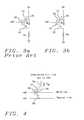
- FIG. 3 ais a schematic of a stacked gate flash memory cell of prior art biased in a program mode
- FIG. 3 bis a schematic of the stacked gate flash memory cell of this invention biased in the program mode
- FIG. 4is a schematic diagram of the stacked gate flash memory cell of this invention biased in a unselected state during programming of another cell along the same wordline,
- FIG. 5is a schematic diagram showing the cells of this invention in a matrix biased in the selected and unselected state
- FIG. 6 ais a schematic of a stacked gate flash memory cell of prior art biased in an erase mode
- FIG. 6 bis a schematic of a stacked gate flash memory cell of this invention biased in the erase mode
- FIG. 7is a method to produce the stacked gate flash memory cell of this invention.
- FIG. 1a cross sectional view of the stacked gate flash memory cell of this invention.
- a floating gate 10is formed on a gate oxide 11 grown on a semiconductor substrate 14 .
- a control gate 12On top of the floating gate 10 is a control gate 12 separated from the floating gate by an oxide 13 .
- Sidewalls 15are formed on the stacked gate comprising the floating gate 10 and control gate 12 .
- Implanted in the semiconductor substrate 14is an N+ drain 16 extending under a sidewall 15 to a region under the edge of one side of the floating gate 10 .
- an N ⁇ lightly doped drain (LDD) 17is implanted into the semiconductor.
- substrateextending under the sidewall 15 to a region under the edge of the opposite side of the floating gate 10 .
- LDDlightly doped drain
- Both the N+ source 16 and the N-LDD 17were implanted into the substrate before the sidewalls 15 were formed on the sides of the stacked floating gate 10 and control gate 12 . After the sidewalls 15 are formed an N+ drain 18 is implanted into the semiconductor substrate 14 .
- the electric field of the drain junctionis reduced which reduces the hot electron generation at the drain and reduces the bit line disturb conditions during program operations.
- FIG. 2 aa schematic of bias conditions for a read operation is shown for prior art.
- a stacked gate transistor flash memory cell 20is biased with IV connected to the drain 21 , Vcc connected to the control gate 22 by means of a wordline (not shown for simplicity), and ground connected to the source 23 through a source line (not shown for simplicity).
- the resistance Rsrepresents the resistance of the source line.
- FIG. 2 bis shown the stacked gate flash memory cell of this invention biased in a read mode.
- the stacked gate transistor 30is biased similar to the transistor 20 of prior art shown in FIG. 2 a .
- the control gate 32is biased to Vcc through a connecting wordline (not shown for simplicity) and the source 33 is biased to ground through a connecting source line (not shown for simplicity) where the source line resistance is Rs.
- the drain 31is biased greater than 1.5 volts as a result of the low concentration ions in the drain junction resulting from the N-LDD 17 which allows a stronger bit current to reduce read errors and improve read speed.
- the increased drain voltagecan allow a longer and/or a more resistive bit line to be used.
- FIG. 3 ais shown a stacked gate flash memory cell of prior art biased in program mode.
- the stacked gate transistor 40is biased to +5V on the drain 41 , to +9V on the control gate 42 , and to ground on the source 43 through a source line with a resistance of Rs.
- a current IDSflows through the stacked gate transistor 40 .
- the stacked gate transistor 50 of the flash memory cell of this inventionis shown in FIG. 3 b .
- the drain 51is connected to 0V through a bit line (not shown for simplicity)
- the control gateis biased to +9V through a wordline (not shown for simplicity)
- the source 53is biased to +5V through a source line (not shown for simplicity) where Rs represents the resistance of the source line.
- the current I SDFlows in an opposite direction compared to that in the transistor 40 of prior art. Even though the drain junction 17 of the stacked gate transistor 50 in FIG. 3 b sees the floating gate, the low concentration of ions in the LDD does not allow an efficient generation of hot electrons for programming the floating gate 54 of the stacked gate transistor 50 .
- the stacked gate of prior art shown in FIG. 3 auses the drain 41 for hot electron programming and the source 43 for Fowler-Nordheim (FN) tunneling for erase operations.
- the stacked gate flash memory cell of this invention shown in FIG. 3 buses the source 53 for both hot electron programming and FN tunneling for erasing.
- the gate to source voltage V Gs9 ⁇ (5 ⁇ I SD *R S ) for this invention show in FIG.
- the present inventionhas a higher gate to source voltage that can be used to improve program speed.
- the potential for increased gate to source voltagecan be used to allow a reduced gate voltage which in turn can simplify high voltage design, reduce junction leakage and improve gate disturb.
- FIG. 4is shown a circuit diagram for illustrating a soft program disturb that can occur in this invention.
- An unselected flash memory cell 60is partially biased in a program mode by applying +9V to the control gate 58 by means of a selected wordline and +5V to the source 59 by means of a selected source line.
- the drain 57is biased to +5V which deselects cell for programming.
- +5Vis applied to the unselected bit line 56
- the capacitance C BL of the unselected bit line 56is charged to +5V.
- a transient currentcan flow in the unselected memory cell 60 .
- bit line 56is pre-charged to V cc which minimizes the disturb condition to 5-V cc and a total charge time of less than 0.5us.
- the +5V on the unselected bit line 56will cause a bit line disturb on cell 61 , shown in FIG. 5 .
- the drain side 63 of the stacked gate device 61is engineered to reduce hot carrier generation by means of an LDD 17 shown in FIG. 1 .
- a selected bit line BL 0 55connects a voltage of 0V to the drain 51 connected to the selected cell 50 and to the drain 64 of an unselected cell 62 .
- An unselected bit line BL 1 56connects a voltage of 5V to the drain 57 connected to the selected cell 60 and to the drain 66 of an unselected cell 61 .
- a selected word line WL 0connects +9V to the control gate 52 of the selected cell 50 and to the control gate 58 of an unselected cell 60 .
- a selected source line SL 0connects +5V to the source 53 of the selected stacked gate flash memory cell 50 , to the source 65 of an unselected cell 62 connected to the selected bit line BL 0 55 , to the source 59 of unselected cell 60 and source 66 of unselected cell 61 .
- An unselected wordline WL 1connects 0V to the gate 67 of the unselected cell 62 and gate 68 of the unselected cell 61 .
- a wordline disturbcan occur on cell 60 , but this disturb condition is minimized because the +5V on the bit line BL 1 and the +5V on the selected source line SL 0 maintain a small channel differential on cell 60 .
- a source line disturbcan occur on unselected cell 62 where the selected source line SL 0 provides +5V to the source 65 of cell 62 .
- the gate 67 of cell 62is bias to 0V by the unselected wordline WL 1 and the drain 64 is biased by the selected bit line BL 0 .
- the source line disturb condition on cell 62is similar to bit line program disturb found in prior art.
- FIG. 6 ais shown the erase configuration for a stacked gate flash memory cell 40 of prior art.
- a bit line(not shown for simplicity) connects a floating line or 0V to the drain 41
- a wordline(not shown for simplicity) connects ⁇ 9V to the gate 42
- a source line(not shown for simplicity) connects +5V to the source 43 of cell 40 where Rs is the resistance of the source line.
- FIG. 6 bis shown the erase configuration for a stacked gate flash memory cell 40 of this invention.
- the configuration to erase information stored on the floating gate of cell 50is similar to that of prior art where a bit line (not shown for simplicity) connects a floating line or 0V to the drain 51 , a wordline (not shown for simplicity) connects ⁇ 9V to the gate 52 and a source line (not shown for simplicity) connects +5V to the source 53 of cell 50 where Rs is the resistance of the source line.
- FIG. 7is shown a method to produce the stacked gate-flash-memory-cell-of this invention.
- a gate oxideis grown on the surface of a semiconductor substrate 80 , and a floating gate is formed on top of the gate oxide 81 .
- an oxide layeris formed on top of the floating gate 82 , which is used to separate the floating gate from a control gate, which is formed on top of the floating gate 83 .
- a lightly doped drainis ion implanted into the semiconductor substrate 84 on the drain side of the gate structure.
- a heavily doped sourceis implanted on the source side of the gate structure 85 and sidewall spacers are formed on the sides of the gate structure 86 . After the sidewalls are formed a heavily doped drain is ion implanted into the semiconductor substrate 87 interfacing the lightly doped drain implanted in step 84 .
Landscapes
- Semiconductor Memories (AREA)
- Non-Volatile Memory (AREA)
- Read Only Memory (AREA)
Abstract
Description
Claims (1)
Priority Applications (2)
| Application Number | Priority Date | Filing Date | Title |
|---|---|---|---|
| US09/531,787US6660585B1 (en) | 2000-03-21 | 2000-03-21 | Stacked gate flash memory cell with reduced disturb conditions |
| US10/616,751US20040008561A1 (en) | 2000-03-21 | 2003-07-10 | Stacked gate flash memory cell with reduced distrub conditions |
Applications Claiming Priority (1)
| Application Number | Priority Date | Filing Date | Title |
|---|---|---|---|
| US09/531,787US6660585B1 (en) | 2000-03-21 | 2000-03-21 | Stacked gate flash memory cell with reduced disturb conditions |
Related Child Applications (1)
| Application Number | Title | Priority Date | Filing Date |
|---|---|---|---|
| US10/616,751DivisionUS20040008561A1 (en) | 2000-03-21 | 2003-07-10 | Stacked gate flash memory cell with reduced distrub conditions |
Publications (1)
| Publication Number | Publication Date |
|---|---|
| US6660585B1true US6660585B1 (en) | 2003-12-09 |
Family
ID=29712407
Family Applications (2)
| Application Number | Title | Priority Date | Filing Date |
|---|---|---|---|
| US09/531,787Expired - LifetimeUS6660585B1 (en) | 2000-03-21 | 2000-03-21 | Stacked gate flash memory cell with reduced disturb conditions |
| US10/616,751AbandonedUS20040008561A1 (en) | 2000-03-21 | 2003-07-10 | Stacked gate flash memory cell with reduced distrub conditions |
Family Applications After (1)
| Application Number | Title | Priority Date | Filing Date |
|---|---|---|---|
| US10/616,751AbandonedUS20040008561A1 (en) | 2000-03-21 | 2003-07-10 | Stacked gate flash memory cell with reduced distrub conditions |
Country Status (1)
| Country | Link |
|---|---|
| US (2) | US6660585B1 (en) |
Cited By (18)
| Publication number | Priority date | Publication date | Assignee | Title |
|---|---|---|---|---|
| US20020123180A1 (en)* | 2001-03-01 | 2002-09-05 | Peter Rabkin | Transistor and memory cell with ultra-short gate feature and method of fabricating the same |
| US20040257877A1 (en)* | 2003-06-20 | 2004-12-23 | Raul-Adrian Cernea | Source controlled operation of non-volatile memories |
| US20050153543A1 (en)* | 2004-01-08 | 2005-07-14 | United Microelectronics Corp | Method of forming self aligned contact |
| US20060245252A1 (en)* | 2005-04-27 | 2006-11-02 | Micron Technology, Inc. | Flash memory programming to reduce program disturb |
| US20070117303A1 (en)* | 2002-08-30 | 2007-05-24 | Fujitsu Limited | Semiconductor memory device (as amended) |
| US20070195603A1 (en)* | 2006-02-22 | 2007-08-23 | Micron Technology, Inc. | Minimizing effects of program disturb in a memory device |
| US20080055980A1 (en)* | 2006-03-08 | 2008-03-06 | Macronix International Co., Ltd. | Method and apparatus for a non-volatile memory device with reduced program disturb |
| DE102006060342A1 (en)* | 2006-12-20 | 2008-06-26 | Texas Instruments Deutschland Gmbh | CMOS transistor |
| US20090046507A1 (en)* | 2006-08-22 | 2009-02-19 | Micron Technology, Inc. | Reducing effects of program disturb in a memory device |
| US20090080246A1 (en)* | 2007-09-25 | 2009-03-26 | Cypress Semiconductor Corporation | Method and apparatus for reduction of bit-line disturb and soft-erase in a trapped-charge memory |
| US20090086538A1 (en)* | 2007-10-02 | 2009-04-02 | Jenne Fredrick B | Method and apparatus for programming memory cell array |
| US20090273979A1 (en)* | 2006-03-28 | 2009-11-05 | Micron Technology, Inc. | Programming method to reduce word line to word line breakdown for nand flash |
| US7729171B2 (en) | 2006-04-12 | 2010-06-01 | Micron Technology, Inc. | Multiple select gate architecture with select gates of different lengths |
| US7733705B2 (en) | 2008-03-13 | 2010-06-08 | Micron Technology, Inc. | Reduction of punch-through disturb during programming of a memory device |
| US9450107B1 (en)* | 2015-09-09 | 2016-09-20 | SK Hynix Inc. | EPROM cells, EPROM cell arrays including the same, and methods of fabricating the same |
| US9449707B2 (en) | 2014-12-19 | 2016-09-20 | Freescale Semiconductor, Inc. | Systems and methods to mitigate program gate disturb in split-gate flash cell arrays |
| CN107978600A (en)* | 2015-10-16 | 2018-05-01 | 力旺电子股份有限公司 | Single-layer polysilicon non-volatile memory element |
| US10146451B2 (en) | 2015-12-10 | 2018-12-04 | SK Hynix Inc. | Reducing read disturb in data storage |
Families Citing this family (3)
| Publication number | Priority date | Publication date | Assignee | Title |
|---|---|---|---|---|
| KR100623185B1 (en)* | 2004-11-19 | 2006-09-19 | 삼성전자주식회사 | Semiconductor device and manufacturing method thereof |
| US7272060B1 (en)* | 2004-12-01 | 2007-09-18 | Spansion Llc | Method, system, and circuit for performing a memory related operation |
| CN104503707B (en) | 2014-12-24 | 2018-03-06 | 华为技术有限公司 | Read the method and device of data |
Citations (21)
| Publication number | Priority date | Publication date | Assignee | Title |
|---|---|---|---|---|
| US5019527A (en)* | 1989-08-11 | 1991-05-28 | Kabushiki Kaisha Toshiba | Method of manufacturing non-volatile semiconductor memories, in which selective removal of field oxidation film for forming source region and self-adjusted treatment for forming contact portion are simultaneously performed |
| US5079603A (en)* | 1986-05-26 | 1992-01-07 | Hitachi, Ltd. | Semiconductor memory device |
| US5168465A (en) | 1988-06-08 | 1992-12-01 | Eliyahou Harari | Highly compact EPROM and flash EEPROM devices |
| US5172200A (en) | 1990-01-12 | 1992-12-15 | Mitsubishi Denki Kabushiki Kaisha | MOS memory device having a LDD structure and a visor-like insulating layer |
| US5194929A (en)* | 1988-03-31 | 1993-03-16 | Kabushiki Kaisha Toshiba | Nonvolatile semiconductor memory and a memory of manufacturing the same |
| US5300802A (en)* | 1988-11-09 | 1994-04-05 | Hitachi, Ltd. | Semiconductor integrated circuit device having single-element type non-volatile memory elements |
| US5345104A (en)* | 1992-05-15 | 1994-09-06 | Micron Technology, Inc. | Flash memory cell having antimony drain for reduced drain voltage during programming |
| US5479036A (en) | 1993-12-02 | 1995-12-26 | United Microelectronics Corporation | Fieldless split-gate EPROM/Flash EPROM |
| US5534455A (en)* | 1994-04-25 | 1996-07-09 | Advanced Micro Devices, Inc. | Method for protecting a stacked gate edge in a semiconductor device from self aligned source (SAS) etch |
| US5654917A (en) | 1995-06-07 | 1997-08-05 | International Business Machines Corporation | Process for making and programming a flash memory array |
| US5674764A (en)* | 1990-08-29 | 1997-10-07 | Texas Instruments Incorporated | Method of making asymmetric non-volatile memory cell |
| US5759896A (en)* | 1996-06-25 | 1998-06-02 | United Microelectronics Corporation | Process for fabricating memory cells of flash memory |
| US5783457A (en)* | 1996-12-27 | 1998-07-21 | United Microelectronics Corporation | Method of making a flash memory cell having an asymmetric source and drain pocket structure |
| US5792670A (en)* | 1993-02-19 | 1998-08-11 | Sgs-Thomson Microelectronics S.R.L. | Method of manufacturing double polysilicon EEPROM cell and access transistor |
| US5880991A (en) | 1997-04-14 | 1999-03-09 | International Business Machines Corporation | Structure for low cost mixed memory integration, new NVRAM structure, and process for forming the mixed memory and NVRAM structure |
| US5882970A (en)* | 1995-11-03 | 1999-03-16 | United Microelectronics Corporation | Method for fabricating flash memory cell having a decreased overlapped region between its source and gate |
| US5920776A (en)* | 1994-07-18 | 1999-07-06 | Sgs-Thomson Microelectronics, S.R.L. | Method of making asymmetric nonvolatile memory cell |
| US6284603B1 (en)* | 2000-07-12 | 2001-09-04 | Chartered Semiconductor Manufacturing Inc. | Flash memory cell structure with improved channel punch-through characteristics |
| US6303454B1 (en)* | 1998-02-02 | 2001-10-16 | Taiwan Semiconductor Manufacturing Company | Process for a snap-back flash EEPROM cell |
| US6330187B1 (en)* | 1998-11-13 | 2001-12-11 | Samsung Electronics, Co., Ltd. | Nonvolatile memory device and method for manufacturing the same |
| US6346441B1 (en)* | 1999-03-19 | 2002-02-12 | United Microelectronics Corp. | Method of fabricating flash memory cell using two tilt implantation steps |
- 2000
- 2000-03-21USUS09/531,787patent/US6660585B1/ennot_activeExpired - Lifetime
- 2003
- 2003-07-10USUS10/616,751patent/US20040008561A1/ennot_activeAbandoned
Patent Citations (21)
| Publication number | Priority date | Publication date | Assignee | Title |
|---|---|---|---|---|
| US5079603A (en)* | 1986-05-26 | 1992-01-07 | Hitachi, Ltd. | Semiconductor memory device |
| US5194929A (en)* | 1988-03-31 | 1993-03-16 | Kabushiki Kaisha Toshiba | Nonvolatile semiconductor memory and a memory of manufacturing the same |
| US5168465A (en) | 1988-06-08 | 1992-12-01 | Eliyahou Harari | Highly compact EPROM and flash EEPROM devices |
| US5300802A (en)* | 1988-11-09 | 1994-04-05 | Hitachi, Ltd. | Semiconductor integrated circuit device having single-element type non-volatile memory elements |
| US5019527A (en)* | 1989-08-11 | 1991-05-28 | Kabushiki Kaisha Toshiba | Method of manufacturing non-volatile semiconductor memories, in which selective removal of field oxidation film for forming source region and self-adjusted treatment for forming contact portion are simultaneously performed |
| US5172200A (en) | 1990-01-12 | 1992-12-15 | Mitsubishi Denki Kabushiki Kaisha | MOS memory device having a LDD structure and a visor-like insulating layer |
| US5674764A (en)* | 1990-08-29 | 1997-10-07 | Texas Instruments Incorporated | Method of making asymmetric non-volatile memory cell |
| US5345104A (en)* | 1992-05-15 | 1994-09-06 | Micron Technology, Inc. | Flash memory cell having antimony drain for reduced drain voltage during programming |
| US5792670A (en)* | 1993-02-19 | 1998-08-11 | Sgs-Thomson Microelectronics S.R.L. | Method of manufacturing double polysilicon EEPROM cell and access transistor |
| US5479036A (en) | 1993-12-02 | 1995-12-26 | United Microelectronics Corporation | Fieldless split-gate EPROM/Flash EPROM |
| US5534455A (en)* | 1994-04-25 | 1996-07-09 | Advanced Micro Devices, Inc. | Method for protecting a stacked gate edge in a semiconductor device from self aligned source (SAS) etch |
| US5920776A (en)* | 1994-07-18 | 1999-07-06 | Sgs-Thomson Microelectronics, S.R.L. | Method of making asymmetric nonvolatile memory cell |
| US5654917A (en) | 1995-06-07 | 1997-08-05 | International Business Machines Corporation | Process for making and programming a flash memory array |
| US5882970A (en)* | 1995-11-03 | 1999-03-16 | United Microelectronics Corporation | Method for fabricating flash memory cell having a decreased overlapped region between its source and gate |
| US5759896A (en)* | 1996-06-25 | 1998-06-02 | United Microelectronics Corporation | Process for fabricating memory cells of flash memory |
| US5783457A (en)* | 1996-12-27 | 1998-07-21 | United Microelectronics Corporation | Method of making a flash memory cell having an asymmetric source and drain pocket structure |
| US5880991A (en) | 1997-04-14 | 1999-03-09 | International Business Machines Corporation | Structure for low cost mixed memory integration, new NVRAM structure, and process for forming the mixed memory and NVRAM structure |
| US6303454B1 (en)* | 1998-02-02 | 2001-10-16 | Taiwan Semiconductor Manufacturing Company | Process for a snap-back flash EEPROM cell |
| US6330187B1 (en)* | 1998-11-13 | 2001-12-11 | Samsung Electronics, Co., Ltd. | Nonvolatile memory device and method for manufacturing the same |
| US6346441B1 (en)* | 1999-03-19 | 2002-02-12 | United Microelectronics Corp. | Method of fabricating flash memory cell using two tilt implantation steps |
| US6284603B1 (en)* | 2000-07-12 | 2001-09-04 | Chartered Semiconductor Manufacturing Inc. | Flash memory cell structure with improved channel punch-through characteristics |
Non-Patent Citations (2)
| Title |
|---|
| Wolf et al., "Hot-Carrier-Resistant Processing and Device Structures", Siicon Processing for the VLSI Era-vol. 3: The Submicron MOSFET, Lattice Press (1995), pp. 595-598.* |
| Wolf et al., "Hot-Carrier-Resistant Processing and Device Structures", Siicon Processing for the VLSI Era—vol. 3: The Submicron MOSFET, Lattice Press (1995), pp. 595-598. |
Cited By (48)
| Publication number | Priority date | Publication date | Assignee | Title |
|---|---|---|---|---|
| US20070148873A1 (en)* | 2001-03-01 | 2007-06-28 | Hynix Semiconductor, Inc. | Method of Forming Transistors with Ultra-short Gate Feature |
| US20080166844A1 (en)* | 2001-03-01 | 2008-07-10 | Hynix Semiconductor, Inc. | Method of Forming a Non-volatile Memory Cell Using Off-set Spacers |
| US20020123180A1 (en)* | 2001-03-01 | 2002-09-05 | Peter Rabkin | Transistor and memory cell with ultra-short gate feature and method of fabricating the same |
| US8288219B2 (en) | 2001-03-01 | 2012-10-16 | Hynix Semiconductor, Inc. | Method of forming a non-volatile memory cell using off-set spacers |
| US8946003B2 (en) | 2001-03-01 | 2015-02-03 | SK Hynix Inc. | Method of forming transistors with ultra-short gate feature |
| US20070117303A1 (en)* | 2002-08-30 | 2007-05-24 | Fujitsu Limited | Semiconductor memory device (as amended) |
| US7482226B2 (en)* | 2002-08-30 | 2009-01-27 | Fujitsu Limited | Semiconductor memory device |
| US20070114617A1 (en)* | 2002-08-30 | 2007-05-24 | Fujitsu Limited | Semiconductor memory device |
| US7759745B2 (en)* | 2002-08-30 | 2010-07-20 | Fujitsu Limited | Semiconductor memory device |
| US7173860B2 (en) | 2003-06-20 | 2007-02-06 | Sandisk Corporation | Source controlled operation of non-volatile memories |
| US20060018184A1 (en)* | 2003-06-20 | 2006-01-26 | Raul-Adrian Cernea | Source controlled operation of non-volatile memories |
| US6950348B2 (en)* | 2003-06-20 | 2005-09-27 | Sandisk Corporation | Source controlled operation of non-volatile memories |
| US20040257877A1 (en)* | 2003-06-20 | 2004-12-23 | Raul-Adrian Cernea | Source controlled operation of non-volatile memories |
| US20050153543A1 (en)* | 2004-01-08 | 2005-07-14 | United Microelectronics Corp | Method of forming self aligned contact |
| US7196930B2 (en) | 2005-04-27 | 2007-03-27 | Micron Technology, Inc. | Flash memory programming to reduce program disturb |
| US20070133294A1 (en)* | 2005-04-27 | 2007-06-14 | Micron Technology, Inc. | Flash memory programming to reduce program disturb |
| US20060245252A1 (en)* | 2005-04-27 | 2006-11-02 | Micron Technology, Inc. | Flash memory programming to reduce program disturb |
| US7630236B2 (en) | 2005-04-27 | 2009-12-08 | Micron Technology, Inc. | Flash memory programming to reduce program disturb |
| US8023329B2 (en) | 2006-02-22 | 2011-09-20 | Micron Technology, Inc. | Reducing effects of program disturb in a memory device |
| US20100202210A1 (en)* | 2006-02-22 | 2010-08-12 | Micron Technology, Inc. | Reducing effects of program disturb in a memory device |
| US7715234B2 (en) | 2006-02-22 | 2010-05-11 | Micron Technology, Inc. | Reducing effects of program disturb in a memory device |
| US20070195603A1 (en)* | 2006-02-22 | 2007-08-23 | Micron Technology, Inc. | Minimizing effects of program disturb in a memory device |
| US20080291730A1 (en)* | 2006-02-22 | 2008-11-27 | Micron Technology, Inc. | Reducing effects of program disturb in a memory device |
| US7408810B2 (en) | 2006-02-22 | 2008-08-05 | Micron Technology, Inc. | Minimizing effects of program disturb in a memory device |
| US7580280B2 (en)* | 2006-03-08 | 2009-08-25 | Macronix International Co., Ltd. | Method and apparatus for a non-volatile memory device with reduced program disturb |
| US20080055980A1 (en)* | 2006-03-08 | 2008-03-06 | Macronix International Co., Ltd. | Method and apparatus for a non-volatile memory device with reduced program disturb |
| US20090273979A1 (en)* | 2006-03-28 | 2009-11-05 | Micron Technology, Inc. | Programming method to reduce word line to word line breakdown for nand flash |
| US7924619B2 (en) | 2006-03-28 | 2011-04-12 | Micron Technology, Inc. | Programming method to reduce word line to word line breakdown for NAND flash |
| US7729171B2 (en) | 2006-04-12 | 2010-06-01 | Micron Technology, Inc. | Multiple select gate architecture with select gates of different lengths |
| US8325520B2 (en) | 2006-08-22 | 2012-12-04 | Micron Technology, Inc. | Reducing effects of program disturb in a memory device |
| US20090046507A1 (en)* | 2006-08-22 | 2009-02-19 | Micron Technology, Inc. | Reducing effects of program disturb in a memory device |
| US7898861B2 (en) | 2006-08-22 | 2011-03-01 | Micron Technology, Inc. | Reducing effects of program disturb in a memory device |
| US8159879B2 (en) | 2006-08-22 | 2012-04-17 | Micron Technology, Inc. | Reducing effects of program disturb in a memory device |
| US20080149982A1 (en)* | 2006-12-20 | 2008-06-26 | Texas Instruments Deutschland Gmbh | Cmos transistor |
| DE102006060342A1 (en)* | 2006-12-20 | 2008-06-26 | Texas Instruments Deutschland Gmbh | CMOS transistor |
| US7706180B2 (en) | 2007-09-25 | 2010-04-27 | Cypress Semiconductor Corporation | Method and apparatus for reduction of bit-line disturb and soft-erase in a trapped-charge memory |
| US7903458B1 (en) | 2007-09-25 | 2011-03-08 | Cypress Semiconductor Corporation | Method and apparatus for reduction of bit-line disturb and soft-erase in a trapped-charge memory |
| US20090080246A1 (en)* | 2007-09-25 | 2009-03-26 | Cypress Semiconductor Corporation | Method and apparatus for reduction of bit-line disturb and soft-erase in a trapped-charge memory |
| US8045373B2 (en) | 2007-10-02 | 2011-10-25 | Cypress Semiconductor Corporation | Method and apparatus for programming memory cell array |
| US20090086538A1 (en)* | 2007-10-02 | 2009-04-02 | Jenne Fredrick B | Method and apparatus for programming memory cell array |
| US20110116311A1 (en)* | 2008-03-13 | 2011-05-19 | Micron Technology, Inc. | Reduction of punch-through disturb during programming of a memory device |
| US8164950B2 (en) | 2008-03-13 | 2012-04-24 | Micron Technology, Inc. | Reduction of punch-through disturb during programming of a memory device |
| US7733705B2 (en) | 2008-03-13 | 2010-06-08 | Micron Technology, Inc. | Reduction of punch-through disturb during programming of a memory device |
| US9449707B2 (en) | 2014-12-19 | 2016-09-20 | Freescale Semiconductor, Inc. | Systems and methods to mitigate program gate disturb in split-gate flash cell arrays |
| US9450107B1 (en)* | 2015-09-09 | 2016-09-20 | SK Hynix Inc. | EPROM cells, EPROM cell arrays including the same, and methods of fabricating the same |
| CN107978600A (en)* | 2015-10-16 | 2018-05-01 | 力旺电子股份有限公司 | Single-layer polysilicon non-volatile memory element |
| CN107978600B (en)* | 2015-10-16 | 2021-04-20 | 力旺电子股份有限公司 | Single-layer polysilicon non-volatile memory element |
| US10146451B2 (en) | 2015-12-10 | 2018-12-04 | SK Hynix Inc. | Reducing read disturb in data storage |
Also Published As
| Publication number | Publication date |
|---|---|
| US20040008561A1 (en) | 2004-01-15 |
Similar Documents
| Publication | Publication Date | Title |
|---|---|---|
| US6660585B1 (en) | Stacked gate flash memory cell with reduced disturb conditions | |
| KR101039244B1 (en) | Nonvolatile Memory and Manufacturing Method Thereof | |
| US7449746B2 (en) | EEPROM with split gate source side injection | |
| US5712180A (en) | EEPROM with split gate source side injection | |
| US5910915A (en) | EEPROM with split gate source side injection | |
| US5416738A (en) | Single transistor flash EPROM cell and method of operation | |
| US5812452A (en) | Electrically byte-selectable and byte-alterable memory arrays | |
| US6144584A (en) | Non-volatile semiconductor memory device and method of manufacturing the same | |
| US7450418B2 (en) | Non-volatile memory and operating method thereof | |
| US7502262B2 (en) | NAND type flash memory array and method for operating the same | |
| US6563736B2 (en) | Flash memory structure having double celled elements and method for fabricating the same | |
| CN113658622B (en) | Writing method of flash memory array | |
| US6091632A (en) | Nonvolatile semiconductor storage device having a plurality of blocks of memory cell transistors formed on respective wells isolated from each other | |
| US6243298B1 (en) | Non-volatile memory cell capable of being programmed and erased through substantially separate areas of one of its drain-side and source-side regions | |
| US6420753B1 (en) | Electrically selectable and alterable memory cells | |
| US6597604B2 (en) | Flash memory cell array and method for programming and erasing data using the same | |
| JPH05206478A (en) | Memory with EEPROM cells having a capacitive effect and a method of reading such cells | |
| US5467307A (en) | Memory array utilizing low voltage Fowler-Nordheim Flash EEPROM cell | |
| KR100706789B1 (en) | Nonvolatile Memory Devices | |
| US7312495B2 (en) | Split gate multi-bit memory cell | |
| US8422290B2 (en) | Methods of reading data in a NAND flash memory device with a fringe voltage applied to a conductive layer | |
| JP3185891B2 (en) | Nonvolatile semiconductor memory device and method of manufacturing the same | |
| KR20000001189A (en) | Program method of nonvolatile memory device |
Legal Events
| Date | Code | Title | Description |
|---|---|---|---|
| AS | Assignment | Owner name:APLUS FLASH TECHNOLOGY, INC., CALIFORNIA Free format text:ASSIGNMENT OF ASSIGNORS INTEREST;ASSIGNORS:LEE, PETER W.;TSAO, HSING-YA;CHAN, VEI-HAN;AND OTHERS;REEL/FRAME:010697/0698 Effective date:20000309 | |
| STCF | Information on status: patent grant | Free format text:PATENTED CASE | |
| FPAY | Fee payment | Year of fee payment:4 | |
| FEPP | Fee payment procedure | Free format text:PAT HOLDER NO LONGER CLAIMS SMALL ENTITY STATUS, ENTITY STATUS SET TO UNDISCOUNTED (ORIGINAL EVENT CODE: STOL); ENTITY STATUS OF PATENT OWNER: LARGE ENTITY | |
| FEPP | Fee payment procedure | Free format text:PAYOR NUMBER ASSIGNED (ORIGINAL EVENT CODE: ASPN); ENTITY STATUS OF PATENT OWNER: LARGE ENTITY Free format text:PAYER NUMBER DE-ASSIGNED (ORIGINAL EVENT CODE: RMPN); ENTITY STATUS OF PATENT OWNER: LARGE ENTITY | |
| AS | Assignment | Owner name:ABEDNEJA ASSETS AG L.L.C., DELAWARE Free format text:ASSIGNMENT OF ASSIGNORS INTEREST;ASSIGNOR:APLUS FLASH TECHNOLOGY, INC.;REEL/FRAME:022562/0920 Effective date:20090224 | |
| FEPP | Fee payment procedure | Free format text:PAYOR NUMBER ASSIGNED (ORIGINAL EVENT CODE: ASPN); ENTITY STATUS OF PATENT OWNER: LARGE ENTITY Free format text:PAYER NUMBER DE-ASSIGNED (ORIGINAL EVENT CODE: RMPN); ENTITY STATUS OF PATENT OWNER: LARGE ENTITY | |
| FPAY | Fee payment | Year of fee payment:8 | |
| FPAY | Fee payment | Year of fee payment:12 | |
| AS | Assignment | Owner name:CALLAHAN CELLULAR L.L.C., DELAWARE Free format text:MERGER;ASSIGNOR:ABEDNEJA ASSETS AG L.L.C.;REEL/FRAME:037513/0535 Effective date:20150826 | |
| AS | Assignment | Owner name:HANGER SOLUTIONS, LLC, GEORGIA Free format text:ASSIGNMENT OF ASSIGNORS INTEREST;ASSIGNOR:INTELLECTUAL VENTURES ASSETS 158 LLC;REEL/FRAME:051486/0425 Effective date:20191206 | |
| AS | Assignment | Owner name:INTELLECTUAL VENTURES ASSETS 158 LLC, DELAWARE Free format text:ASSIGNMENT OF ASSIGNORS INTEREST;ASSIGNOR:CALLAHAN CELLULAR L.L.C.;REEL/FRAME:051727/0155 Effective date:20191126 | |
| AS | Assignment | Owner name:FOOTHILLS IP LLC, COLORADO Free format text:ASSIGNMENT OF ASSIGNORS INTEREST;ASSIGNOR:HANGER SOLUTIONS, LLC;REEL/FRAME:056246/0533 Effective date:20200515 |