US6660391B1 - Low κ dielectric inorganic/organic hybrid films and method of making - Google Patents
Low κ dielectric inorganic/organic hybrid films and method of makingDownload PDFInfo
- Publication number
- US6660391B1 US6660391B1US09/361,667US36166799AUS6660391B1US 6660391 B1US6660391 B1US 6660391B1US 36166799 AUS36166799 AUS 36166799AUS 6660391 B1US6660391 B1US 6660391B1
- Authority
- US
- United States
- Prior art keywords
- film
- dielectric
- low
- dielectric film
- dielectric constant
- Prior art date
- Legal status (The legal status is an assumption and is not a legal conclusion. Google has not performed a legal analysis and makes no representation as to the accuracy of the status listed.)
- Expired - Lifetime
Links
- UVJFYWYLNYRHAO-UHFFFAOYSA-NC1CCCC1.[Rn]Chemical compoundC1CCCC1.[Rn]UVJFYWYLNYRHAO-UHFFFAOYSA-N0.000description2
Images


Classifications
- B—PERFORMING OPERATIONS; TRANSPORTING
- B32—LAYERED PRODUCTS
- B32B—LAYERED PRODUCTS, i.e. PRODUCTS BUILT-UP OF STRATA OF FLAT OR NON-FLAT, e.g. CELLULAR OR HONEYCOMB, FORM
- B32B9/00—Layered products comprising a layer of a particular substance not covered by groups B32B11/00 - B32B29/00
- B32B9/04—Layered products comprising a layer of a particular substance not covered by groups B32B11/00 - B32B29/00 comprising such particular substance as the main or only constituent of a layer, which is next to another layer of the same or of a different material
- C—CHEMISTRY; METALLURGY
- C09—DYES; PAINTS; POLISHES; NATURAL RESINS; ADHESIVES; COMPOSITIONS NOT OTHERWISE PROVIDED FOR; APPLICATIONS OF MATERIALS NOT OTHERWISE PROVIDED FOR
- C09D—COATING COMPOSITIONS, e.g. PAINTS, VARNISHES OR LACQUERS; FILLING PASTES; CHEMICAL PAINT OR INK REMOVERS; INKS; CORRECTING FLUIDS; WOODSTAINS; PASTES OR SOLIDS FOR COLOURING OR PRINTING; USE OF MATERIALS THEREFOR
- C09D4/00—Coating compositions, e.g. paints, varnishes or lacquers, based on organic non-macromolecular compounds having at least one polymerisable carbon-to-carbon unsaturated bond ; Coating compositions, based on monomers of macromolecular compounds of groups C09D183/00 - C09D183/16
- C—CHEMISTRY; METALLURGY
- C23—COATING METALLIC MATERIAL; COATING MATERIAL WITH METALLIC MATERIAL; CHEMICAL SURFACE TREATMENT; DIFFUSION TREATMENT OF METALLIC MATERIAL; COATING BY VACUUM EVAPORATION, BY SPUTTERING, BY ION IMPLANTATION OR BY CHEMICAL VAPOUR DEPOSITION, IN GENERAL; INHIBITING CORROSION OF METALLIC MATERIAL OR INCRUSTATION IN GENERAL
- C23C—COATING METALLIC MATERIAL; COATING MATERIAL WITH METALLIC MATERIAL; SURFACE TREATMENT OF METALLIC MATERIAL BY DIFFUSION INTO THE SURFACE, BY CHEMICAL CONVERSION OR SUBSTITUTION; COATING BY VACUUM EVAPORATION, BY SPUTTERING, BY ION IMPLANTATION OR BY CHEMICAL VAPOUR DEPOSITION, IN GENERAL
- C23C16/00—Chemical coating by decomposition of gaseous compounds, without leaving reaction products of surface material in the coating, i.e. chemical vapour deposition [CVD] processes
- C23C16/22—Chemical coating by decomposition of gaseous compounds, without leaving reaction products of surface material in the coating, i.e. chemical vapour deposition [CVD] processes characterised by the deposition of inorganic material, other than metallic material
- C23C16/30—Deposition of compounds, mixtures or solid solutions, e.g. borides, carbides, nitrides
- C23C16/40—Oxides
- C23C16/401—Oxides containing silicon
- H—ELECTRICITY
- H01—ELECTRIC ELEMENTS
- H01L—SEMICONDUCTOR DEVICES NOT COVERED BY CLASS H10
- H01L21/00—Processes or apparatus adapted for the manufacture or treatment of semiconductor or solid state devices or of parts thereof
- H01L21/02—Manufacture or treatment of semiconductor devices or of parts thereof
- H01L21/02104—Forming layers
- H01L21/02107—Forming insulating materials on a substrate
- H01L21/02109—Forming insulating materials on a substrate characterised by the type of layer, e.g. type of material, porous/non-porous, pre-cursors, mixtures or laminates
- H01L21/02112—Forming insulating materials on a substrate characterised by the type of layer, e.g. type of material, porous/non-porous, pre-cursors, mixtures or laminates characterised by the material of the layer
- H01L21/02123—Forming insulating materials on a substrate characterised by the type of layer, e.g. type of material, porous/non-porous, pre-cursors, mixtures or laminates characterised by the material of the layer the material containing silicon
- H01L21/02126—Forming insulating materials on a substrate characterised by the type of layer, e.g. type of material, porous/non-porous, pre-cursors, mixtures or laminates characterised by the material of the layer the material containing silicon the material containing Si, O, and at least one of H, N, C, F, or other non-metal elements, e.g. SiOC, SiOC:H or SiONC
- H—ELECTRICITY
- H01—ELECTRIC ELEMENTS
- H01L—SEMICONDUCTOR DEVICES NOT COVERED BY CLASS H10
- H01L21/00—Processes or apparatus adapted for the manufacture or treatment of semiconductor or solid state devices or of parts thereof
- H01L21/02—Manufacture or treatment of semiconductor devices or of parts thereof
- H01L21/02104—Forming layers
- H01L21/02107—Forming insulating materials on a substrate
- H01L21/02109—Forming insulating materials on a substrate characterised by the type of layer, e.g. type of material, porous/non-porous, pre-cursors, mixtures or laminates
- H01L21/02205—Forming insulating materials on a substrate characterised by the type of layer, e.g. type of material, porous/non-porous, pre-cursors, mixtures or laminates the layer being characterised by the precursor material for deposition
- H01L21/02208—Forming insulating materials on a substrate characterised by the type of layer, e.g. type of material, porous/non-porous, pre-cursors, mixtures or laminates the layer being characterised by the precursor material for deposition the precursor containing a compound comprising Si
- H01L21/02211—Forming insulating materials on a substrate characterised by the type of layer, e.g. type of material, porous/non-porous, pre-cursors, mixtures or laminates the layer being characterised by the precursor material for deposition the precursor containing a compound comprising Si the compound being a silane, e.g. disilane, methylsilane or chlorosilane
- H—ELECTRICITY
- H01—ELECTRIC ELEMENTS
- H01L—SEMICONDUCTOR DEVICES NOT COVERED BY CLASS H10
- H01L21/00—Processes or apparatus adapted for the manufacture or treatment of semiconductor or solid state devices or of parts thereof
- H01L21/02—Manufacture or treatment of semiconductor devices or of parts thereof
- H01L21/02104—Forming layers
- H01L21/02107—Forming insulating materials on a substrate
- H01L21/02109—Forming insulating materials on a substrate characterised by the type of layer, e.g. type of material, porous/non-porous, pre-cursors, mixtures or laminates
- H01L21/02205—Forming insulating materials on a substrate characterised by the type of layer, e.g. type of material, porous/non-porous, pre-cursors, mixtures or laminates the layer being characterised by the precursor material for deposition
- H01L21/02208—Forming insulating materials on a substrate characterised by the type of layer, e.g. type of material, porous/non-porous, pre-cursors, mixtures or laminates the layer being characterised by the precursor material for deposition the precursor containing a compound comprising Si
- H01L21/02214—Forming insulating materials on a substrate characterised by the type of layer, e.g. type of material, porous/non-porous, pre-cursors, mixtures or laminates the layer being characterised by the precursor material for deposition the precursor containing a compound comprising Si the compound comprising silicon and oxygen
- H01L21/02216—Forming insulating materials on a substrate characterised by the type of layer, e.g. type of material, porous/non-porous, pre-cursors, mixtures or laminates the layer being characterised by the precursor material for deposition the precursor containing a compound comprising Si the compound comprising silicon and oxygen the compound being a molecule comprising at least one silicon-oxygen bond and the compound having hydrogen or an organic group attached to the silicon or oxygen, e.g. a siloxane
- H—ELECTRICITY
- H01—ELECTRIC ELEMENTS
- H01L—SEMICONDUCTOR DEVICES NOT COVERED BY CLASS H10
- H01L21/00—Processes or apparatus adapted for the manufacture or treatment of semiconductor or solid state devices or of parts thereof
- H01L21/02—Manufacture or treatment of semiconductor devices or of parts thereof
- H01L21/02104—Forming layers
- H01L21/02107—Forming insulating materials on a substrate
- H01L21/02225—Forming insulating materials on a substrate characterised by the process for the formation of the insulating layer
- H01L21/0226—Forming insulating materials on a substrate characterised by the process for the formation of the insulating layer formation by a deposition process
- H01L21/02263—Forming insulating materials on a substrate characterised by the process for the formation of the insulating layer formation by a deposition process deposition from the gas or vapour phase
- H01L21/02271—Forming insulating materials on a substrate characterised by the process for the formation of the insulating layer formation by a deposition process deposition from the gas or vapour phase deposition by decomposition or reaction of gaseous or vapour phase compounds, i.e. chemical vapour deposition
- H01L21/02274—Forming insulating materials on a substrate characterised by the process for the formation of the insulating layer formation by a deposition process deposition from the gas or vapour phase deposition by decomposition or reaction of gaseous or vapour phase compounds, i.e. chemical vapour deposition in the presence of a plasma [PECVD]
- Y—GENERAL TAGGING OF NEW TECHNOLOGICAL DEVELOPMENTS; GENERAL TAGGING OF CROSS-SECTIONAL TECHNOLOGIES SPANNING OVER SEVERAL SECTIONS OF THE IPC; TECHNICAL SUBJECTS COVERED BY FORMER USPC CROSS-REFERENCE ART COLLECTIONS [XRACs] AND DIGESTS
- Y10—TECHNICAL SUBJECTS COVERED BY FORMER USPC
- Y10T—TECHNICAL SUBJECTS COVERED BY FORMER US CLASSIFICATION
- Y10T428/00—Stock material or miscellaneous articles
- Y10T428/24—Structurally defined web or sheet [e.g., overall dimension, etc.]
- Y10T428/24802—Discontinuous or differential coating, impregnation or bond [e.g., artwork, printing, retouched photograph, etc.]
- Y10T428/24917—Discontinuous or differential coating, impregnation or bond [e.g., artwork, printing, retouched photograph, etc.] including metal layer
- Y—GENERAL TAGGING OF NEW TECHNOLOGICAL DEVELOPMENTS; GENERAL TAGGING OF CROSS-SECTIONAL TECHNOLOGIES SPANNING OVER SEVERAL SECTIONS OF THE IPC; TECHNICAL SUBJECTS COVERED BY FORMER USPC CROSS-REFERENCE ART COLLECTIONS [XRACs] AND DIGESTS
- Y10—TECHNICAL SUBJECTS COVERED BY FORMER USPC
- Y10T—TECHNICAL SUBJECTS COVERED BY FORMER US CLASSIFICATION
- Y10T428/00—Stock material or miscellaneous articles
- Y10T428/31504—Composite [nonstructural laminate]
- Y10T428/31652—Of asbestos
- Y10T428/31663—As siloxane, silicone or silane
Definitions
- This inventionrelates to materials having low dielectric constants. More specifically, the present invention relates to inorganic/organic hybrid films having low dielectric constant for use in semiconductors, produced using organosilicon precursors, and a method for making the same.
- Dielectric film layersare fundamental components of integrated circuits and semiconductors. Such films provide electrical isolation between components. As device densities increase, multiple layer dielectric films are generally used to isolate device features. When forming dielectric films it is important for the film to exhibit certain properties, such as good gap fill, thermal stability and favorable electrical properties.
- silicon dioxideSiO 2
- CVDchemical vapor deposition
- plasma CVDplasma CVD
- the dielectric constant ( ⁇ ) of the dielectric materialacquires increasing importance. For example, as the industry moves to smaller interconnects and device features, the actual length of the interconnecting lines increases and the space between them decreases. These trends increase the RC delay of the circuit.
- devicesmay incorporate five or six dielectric layers, all comprised of silicon dioxide.
- Silicon dioxide (SiO 2 )has a relatively high dielectric constant at about 4.0.
- Replacing SiO 2 with a suitable low dielectric constant (low ⁇ ) materialwill lead to a dramatic improvement in speed and reduction in the power consumption of the device.
- Such advanced low dielectric materialswould play an important role in enabling the semiconductor industry to develop the next generation of devices.
- fluorinated amorphous carbonsAnother plasma CVD approach to create low ⁇ films is the deposition of highly crosslinked fluorocarbon films, commonly referred to as fluorinated amorphous carbons.
- the dielectric constant of the more promising versions of such filmshas generally been reported as between 2.5 to 3.0 after the first anneal. Issues for fluorinated amorphous carbon remain, most notably with adhesion; the thermal stability, including dimensional stability; and the integration of the films.
- Polymeric materialshave also been investigated. For example, spin coated polymeric materials have been employed. Despite their lower ⁇ values, these polymers are not entirely satisfactory due to processing and material limitations. Polymers are generally thermally and dimensionally unstable at standard processing conditions of about 400 to 450° C. While these materials have been considered for embedded structures, as a rule they are not suitable for full stack gap fill or damascene structures.
- vapor phase polymerizationhas been explored as an alternative method for the preparation of low ⁇ materials.
- One particular class of polymers which has been prepared through vapor phase polymerizationare the polyxylylenes (also known as parylenes) such as parylene N (ppx-N), and parylene F (ppx-F).
- Paryleneshave ⁇ values ranging from 2.3 to 2.7 and are thus attractive as low dielectric materials for use in integrated circuits.
- the parylenes that have been prepared to dateexhibit poor thermal stability as with ppx-N; expensive as with ppx-F, or have issues with mechanical stability.
- a dielectric filmcomprised of an inorganic/organic hybrid material having a low dielectric constant and good thermal stability for use in semiconductors and integrated circuits.
- Another object of the present inventionis to employ precursors of organosilicon, such as siloxanes, to form an inorganic/organic hybrid dielectric material having a low ⁇ and good thermal stability for use in semiconductor and/or integrated circuit applications.
- organosiliconsuch as siloxanes
- a further object of the present inventionis to provide a method of depositing a dielectric layer for use in semiconductor and integrated circuit application having an inorganic/organic hybrid material with a low dielectric constant.
- an improved dielectric film of the present inventionhaving a low dielectric constant, formed as a film in a semiconductor and/or integrated circuit and comprised of a combination of inorganic and organic functionality. More specifically, the film is formed of a backbone structure made substantially of Si—O—Si and organic side groups attached to the backbone structure. In an alternative embodiment, the film is formed of a backbone structure made substantially of Si—N—Si groups and organic side groups attached to the backbone structure.
- organosilicon precursorsare used to form a dielectric film for use in semiconductors and/or integrated circuits having a backbone comprised of substantially Si—O—Si or Si—N—Si groups and organic side groups.
- a method of depositing a dielectric film in a semiconductor and/or integrated circuit by chemical vapor deposition (CVD)is provided.
- the filmis deposited in a manner such that the film is comprised of a backbone made substantially of Si—O—Si or Si—N—Si groups with organic side groups attached to the backbone.
- a method of fabricating a film having multiple layerscomprises the steps of forming a film comprised of: at least one low ⁇ dielectric layer in the semiconductor or integrated circuit device having a combination of inorganic and organic materials and exhibiting a low dielectric constant, and forming insitu at least one oxide layer either directly above and/or directly below each low ⁇ dielectric layer to form the multilayered film.
- the oxide layermay be formed insitu by simply varying the process conditions.
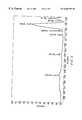
- FIG. 1is a schematic drawing of the structure of the film in accordance with one embodiment of the present invention.
- FIG. 2is a schematic view showing an example of a reactor that may be used to carry out the present invention.
- FIG. 3is a FTIR scan showing the composition of a film in accordance with one embodiment of the present invention.
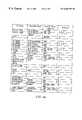
- FIG. 4 ais a table illustrating FTIR peak ranges and their assignments according to the literature.
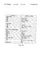
- FIG. 4 bis a table showing one interpretation of an FTIR plot of a film in accordance with the present invention.
- Low dielectric constant ( ⁇ ) filmsfor use in the semiconductor industry, and their method of fabrication, are provided.
- the term “low ⁇ dielectric,” “low dielectric constant,” and “low ⁇ ”are used interchangeably and typically mean a dielectric constant of less than 4.0.
- the term “very low dielectric constant” (vl ⁇ )is typically considered to be a dielectric constant of equal to or less than 3.0.
- low ⁇ and very low ⁇ dielectric filmsare comprised of a combination of inorganic and organic properties. More particularly, the inorganic/organic hybrid films are comprised of silicon, oxygen and/or nitrogen, carbon and hydrogen; or alternatively silicon, oxygen and or nitrogen, carbon and fluorine.
- the structure of the filmis of randomly mixed organic and inorganic groups.
- the groupsmay be cross linked.
- the groupsmay be present in a three dimensional matrix.
- the filmis formed having a backbone structure made substantially of inorganic Si—O—Si groups, with organic side groups attached to the backbone.
- the filmis formed of a backbone structure made substantially of Si—N—Si groups and organic side groups attached to the backbone structure.
- the backboneis present in a three dimensional network with cyclic Si—O—Si groups connected by inorganic chains, to form a ring (or other three dimensional structure such as a ball, cube and the like) and chain structure.
- the inorganic chainsmay be comprised substantially of Si—O—Si groups, or alternatively, of Si—N—Si groups.
- the inorganic chainsmay vary in length and composition.
- Organic side groupsare attached to either, or both of, the cyclic and chain groups.
- the filmis comprised of a series of siloxane chains (no cyclic groups) with organic side groups attached.
- the chainsmay be cross linked.
- the organic side groups recited aboveare generally comprised of carbon chains. More specifically, the organic side groups are selected from the group consisting of aliphatic, olefinic and aromatic hydrocarbons, and aliphatic, olefinic and aromatic fluorocarbons.
- the side groupsdo not have to be comprised of identical units, but may be a combination of different organic groups.
- the organic side groupsare comprised substantially of methyl (CH 3 ) or carbon tri fluoride (CF 3 ) groups.
- the ring and chain structureis shown.
- the ringis the cyclic component which in this example is comprised of four silicon atoms.
- the ringsare connected by inorganic chains.
- the chainsmay vary in length, and in this example, the chains are Si—O—Si groups.
- the backbone of the structureis comprised of Si—O—Si cyclic ring and chain groups.
- Organic side groupsare attached to both the ring and chain groups, and in this example the organic side groups are comprised of methyl groups.
- the structure of the filmis a random network. Referring again to FIG. 1, only a portion of the film is shown. At each end, the structure continues and may be connected to more rings, long or short chains, or a combination of all of the above.
- the ratio of silicon to carbon in the filmis in the range of approximately 0.25:1 to 4:1.
- the density of silicon in the chain groups to silicon in the cyclic groupsis estimated to be in the range of approximately 10:1 to 0.1:1.
- the low ⁇ film of the present inventionwill have a structure comprised of cyclic and chain groups.
- This mixture of cyclic and chain groupsprovides a significant advance over the prior art films.
- the inventorshave found a method that preserves the presence of the cyclic units in the film, which lowers the dielectric constant of the film. Further, the inventors have found that minimizing the C—C bonding in the film structure, allows the addition of organic materials into the film without significantly adversely affecting the thermal stability of the film at temperatures of 450° C. As shown in FIG. 1 there is an absence of carbon to carbon bonding.
- the films produced by the present inventionexhibit desirable dielectric constants while maintaining good thermal stability.
- the dielectric constant of the filmis less than 4.0, preferably less than 3.0, with a dielectric constant in the range of approximately less than 3.0 to 1.5 being most preferred.
- films tested with a dielectric constant of 3.0exhibit good thermal stability as measured by weight loss of less than 1% per 8 hours at 425° C. in a nitrogen environment.
- organosilicon precursor chemistryis used, or alternatively, mixtures that contain an organosilicon precursor(s) may be used.
- organosilicon precursors of the formula belowmay be used to form the film of the invention:
- suitable aliphatic, olefinic, and aromatic hydrocarbon groupsinclude methyl, ethyl, propyl, butyl, and phenyl, etc.
- the organosilicon precursormay be comprised of cyclic organosiloxanes of the formula:
- the organosilicon precursoris comprised of organosilazanes of the formula:
- the organosilicon precursoris comprised of organosilazanes of the formula
- organosilazanemay be linear or branched;, and n is 1 to (3m+4); m is 1 to 4; X is selected from the group consisting of H and the halogens; R is selected from the group consisting of aliphatic, olefinic and aromatic hydrocarbons, and aliphatic, olefinic and aromatic fluorocarbons.
- the organosilicon precursoris comprised of cyclic organosilazanes of the formula:
- Xis selected from the group consisting of H and the halogens;
- Ris selected from the group consisting of aliphatic, olefinic and aromatic hydrocarbons, and aliphatic, olefinic and aromatic fluorocarbons.
- suitable precursors according to the inventioninclude: organic siloxanes, fluorosiloxanes, cyclosiloxanes, fluorine containing cyclosiloxanes, organosilazanes, fluorosilazanes, cyclosilazane, silicates, TEOS, and TMS and mixtures thereof.
- suitable side groupsinclude: —H, —CH 3 , —F, —C 2 H 5 , —CF 3 , —C 2 F 5 , —C 6 H 5 , —C 6 F 5 , —CF 2 CF 3 , and C—H 2 CF 3 .
- Combinations of chemicals that when mixed in a reactorcould create similar chemical constituents in final form as the aforementioned precursors, for example a mixture of: silane, silicon tetra fluoride and an organic precursor are also suitable.
- the present inventionprovides for minimizing the fragmentation of the precursor, thus preserving the general structure deposited in the film.
- precursors with components that form a film structure having an inorganic backbone with organic side groupsmay be used. Accordingly, to form inorganic/organic hybrid films comprised of SiOC, in one embodiment of the present invention, it is preferred to deposit the films from organosilicon precursors in a plasma CVD reactor. Fluorine substitutes of the above materials may also be used.
- the organosilicon precursorsmay be saturated or unsaturated. Examples of organosilicon precursors that are suitable according to the invention include hexamethyl disiloxane (HMDSO), 1,1,3,3-tetramethyldisiloxane (TMDSO) and the like. Other organosilicon precursors such as tetraethyoxysilane (TEOS) may also be used.
- HMDSOhexamethyl disiloxane
- TMDSO1,1,3,3-tetramethyldisiloxane
- TEOStetraethyoxysilane
- the materials mentionedare generally inexpensive and readily available. These materials
- the film of the invention having the ring and chain structureis formed by cyclic organosilicon or cyclic organosilazane precursors.
- the cyclic organosilicon or organosilazanemay be substituted with one or more fluorine atoms. Further, they may be saturated or unsaturated.
- Suitable cyclic organosiliconsinclude: cyclosiloxanes such as octamethylcyclotetrasiloxane (OMCTS), hexa methyl cyclo trisiloxane, hexa phenyl cyclo trisiloxane, octa phenyl cyclo tetrasiloxane, 1,3,5-trimethyl- 1,3,5-tris-3,3,3-trifluoropropyl cyclo trisiloxane, fluorine containing cyclosiloxanes, and combinations of chemicals that create the same chemical components as above.
- Organosilazane precursorsmay also be used.
- the precursoris octamethylcyclotetrasiloxane (OMCTS).
- OCTSoctamethylcyclotetrasiloxane
- the inventionprovides for the formation of a film that preserves part of the structure of the precursor.
- the filmis formed with a ring and chain structure which is a three dimensional network structure.
- This three dimensional network structurereduces the density of the film, which in turn further reduces the dielectric constant and increases the thermal stability of the film. It is important to note that while the three dimensional network structure is typically referred to herein as a ring, any three dimensional structure may be present, such as a ball or cube structure.
- Fluorinated filmscan be formed by the present invention by adding fluorinating materials to the system. This can be accomplished in two ways. First, fluorinating gases can be added to the plasma in the reactor. Suitable fluorinating gases are NF 3, CF 4 , SiF 4 and the like. Second, fluorinated precursors can be added to the reactor. For example, fluorosiloxane or cyclofluorosiloxane precursors can be used alone or can be mixed with linear or cyclic organosilicons or organosilazanes to form a fluorinated film.
- the present inventionprovides a method of depositing a low ⁇ dielectric film comprised of both inorganic and organic nature for use in semiconductor and integrated circuit applications.
- the filmis comprised of an inorganic backbone with organic side groups.
- the backbonemay be linear, or comprised of a combination of three dimensional structures (such as a ring, ball, cube, and the like) and chains.
- the filmis formed by chemical vapor deposition (CVD), and preferably the film is deposited by plasma CVD in a plasma CVD reactor.
- CVDchemical vapor deposition
- the present inventionprovides for an improved CVD method which is a method of depositing a film that retains, in part, the structure of the precursor material.
- the method of the present inventiondeposits a film that retains part of the cyclic structure of the precursor. As discussed above this is particularly advantageous since such a structure promotes low ⁇ properties in the deposited film.
- a reactorsuch as that illustrated in FIG. 2 is employed to deposit the film of the present invention.
- the reactor 5includes a plasma chamber 10 and a process chamber 11 .
- the plasma chamber 10includes a plasma source 12 for coupling energy, ranging from d.c. to microwave, via generator 13 into the plasma chamber 10 to excite a gas into a plasma.
- the plasma source 12is represented by a coil arranged around the plasma chamber 10 and energized with rf energy, however, it is to be understood by those of ordinary skill in the art that various types of plasma sources known in the art may be used to generate a plasma.
- a substrate 14is placed on a support 16 and is positioned in the process chamber 11 .
- the support 16may be biased by application of power through r.f. and/or d.c. generator 18 .
- the support 16may be an electrostatic chuck.
- the chambers 10 and 11are evacuated through port 22 .
- the chemical precursorsare injected into the process chamber 11 via gas inlet line 24 .
- the precursors or other gasesmay be injected into the plasma chamber 10 via gas inlet 26 .
- the organosilicon precursors according to the present inventionare present in liquid form under atmospheric conditions, the liquid is passed though a vaporizer 28 to vaporize the precursor prior to its introduction into the chamber 11 .
- the liquid organosilicon precursormay be introduced into the chamber through a bubbler.
- diluent gases and/or oxidizing gasesmay be added via inlet 27 to the reactor 5 .
- the plasma sourcepartially ionizes the precursor. It is important that the plasma conditions be controlled in such a manner that the precursor is not highly fragmented nor overly oxidized. This is in direct contrast to prior art CVD processes where one generally wants to fragment the precursor as much as possible when depositing a dielectric film.
- a high level of fragmentation of an organosilicon precursorwill generally lead to the deposition of a silicon dioxide type material with a high dielectric constant. This is especially true if a certain concentration of oxygen is present in the plasma.
- the semiconductor substrateis positioned in the process chamber where it is exposed to the precursor which reacts and deposits a film on the surface by CVD.
- the precursorwill be injected into the process chamber proximate to the substrate surface, such as through a gas ring to enhance the uniformity of the deposited film.
- the precursormay be a single chemical, or alternatively, a plurality of chemicals. It has been found that the addition of oxygen can enhance the thermal stability of the film. The exact concentration of oxygen added is dependent on processing conditions and the system configuration.
- inert gasesare not added to the system in contrast to prior art systems. It has been found that the addition of argon generally has a detrimental effect on the film. Argon ionizes to a high degree and causes the precursor to fragment. This in turn leads to films with higher dielectric constants. Conversely, the addition of helium has been found in some cases to have a dramatically reduced impact on the dielectric constant, and further may enhance the thermal stability of the film.
- the process conditionsare important to depositing the film of the present invention.
- the factors of most importanceare the power and pressure of the system, and the organosilicon flow rate, and the oxygen to organosilicon flow rate ratio.
- the exact process conditionswill vary depending on the type and design of the reactor used.
- the plasma chamberincludes a plasma source, and the excitation is at a power density in the range of 200 to 20,000 W/ft 3 .
- the process conditionsare strongly a function of the precursor employed and the design of the reactor. For example, in the case of a plasma system, low excitation power generally produces organic films and higher powers produce more thermally stable films.
- the filmbecomes SiO 2 -like and the dielectric constant becomes too high. If the excitation power is too low then the thermal stability will be undesirably poor. Further when the power is too low, or the plasma chemistry has not been properly determined, it is possible under some circumstances to create undesirable groups in the films. Under such conditions peaks associated with Si—OH have been observed in the FTIR spectra and the dielectric constant is higher than desired. Also, the role of oxygen in the process is to improve the thermal stability of the film. The amount of oxygen will vary depending on the reactor and process conditions used. For example, the percent concentration of oxygen used is a function of the process conditions, such as the rf power, pressure, and the flow rate of the organosilicon precursor.
- Too much oxygenwill result in a film that is a SiO 2 -like material. Too little oxygen generally results in a film with more organic nature than desirable, which lowers the thermal stability of the film and may result in the formation of undesirable groups in the film such as —OH.
- thermal CVD reactorsmay be used that operate at either atmospheric pressure, sub-atmospheric pressure or at low pressure conditions.
- the organosiliconis degraded thermally in the presence of an oxidizing agent. Control of the chamber temperature, the nature of the oxidizing agent (such as ozone, hydrogen peroxide, and/or oxygen), and the concentration of the oxidizing agent is fundamental for producing low ⁇ films.
- another embodiment of the present inventionprovides for a method of fabricating a film having multiple layers. It may be advantageous in certain applications to provide a film that has multiple layers where an oxide (such as SiO 2 or SiO 2 -like) is formed along with a low ⁇ dielectric film to form the multilayered film.
- the oxide layercan be formed above or below the low ⁇ dielectric layer to provide a protective layer, or to improve adhesion.
- at least one oxide, or oxide like layeris formed insitu either directly above and/or directly below a low ⁇ dielectric layer.
- the low ⁇ dielectric layeris comprised of a combination of inorganic and organic materials.
- the low ⁇ dielectric filmis as formed as described above.
- the layer of oxide or silicon dioxidemay be formed insitu by simply varying the process conditions in the reactor.
- the process conditionscan be employed in two ways. First, a SiO 2 deposition process as known in the art can be used. Second, the method of the present invention can be varied to cause substantial fragmentation of the precursor to occur which results in a SiO 2 or SiO 2 type film to de deposited. The method can be varied to cause substantial fragmentation of the precursor in a number of ways, such as by exposing the precursor to a higher plasma power density, by increasing the flow rate of oxygen, by adding argon, or by a combination of any of the same.
- the SiO 2 layercan be formed at any suitable position within the multilayered film.
- the multilayered filmis then formed at any suitable position within a semiconductor device.
- the SiO 2 layercan be formed directly below the desired low ⁇ film to improve the adhesion properties, with the low ⁇ film being formed directly atop the SiO 2 layer.
- the SiO 2 layercan be formed as the top layer in a device to provide a protective layer, or to aid in further processing such as chemical mechanical planarization or etching.
- a very low ⁇ dielectric film according the present inventionwas formed on a 4′′ silicon wafer in a cylindrical plasma reactor using octamethylcyclotetrasiloxane (OMCTS) and oxygen combined in a plasma discharge generated at a frequency of 13.56 MHz.
- OCTSoctamethylcyclotetrasiloxane
- the silicon waferwas placed on a substrate holder made of copper which was electrically isolated during the deposition process.
- the waferwas secured onto the substrate holder with a vacuum compatible adhesive and placed into the deposition chamber.
- the deposition chamberwas 8′′ in diameter and 8′′ in length and contains a hollow cathode electrode system which was centered to the center of the silicon wafer.
- the chamberwas evacuated with a rotary vane pump to a pressure less than 20 mTorr.
- the OMCTS liquidwas injected into a heated stainless steel vaporizing system which vaporized the material to form a vapor stream which was then controllably flowed into the plasma reactor at a flow rate of approximately 8 sccm (standard cubic centimeters per minute).
- oxygen gasfrom a compressed gas cylinder with a purity of 99.95% was controllably flowed into the reactor through the same gas inlet as the OMCTS at 5 sccm.
- the resulting pressure in the reactorwas approximately 150 mTorr.
- a plasmawas then ignited with 300 watts of power with a 13.56 MHz power supply and the plasma discharge was maintained for approximately 5 minutes, during which time, a film was deposited on the surface of the wafer.
- the filmwas deposited to a thickness of 5000 ⁇ .
- the filmwas measured using elipsometry to measure thickness, and using aluminum dot techniques to measure the dielectric constant.
- the testsyielded a dielectric constant of 2.6.
- Additional films in accordance with the inventionwere deposited on wafers under the same conditions and procedure as outlined above, and then measured for thermal weight loss by heating at 400 C. for 1 hour.
- the filmsexhibited a loss of 2.0 weight %.
- the filmssubsequently underwent a thermal cycle of 1 hour at 425 C. and 1 hour at 450 C.
- the weight loss in each instancewas approximately 0.4% per hour, thereby indicating a desirable dielectric constant and thermal stability.
- low ⁇ dielectric filmswere deposited in accordance with another embodiment of the inventive method where the flow rate of the precursors and the plasma conditions were changed.
- the reactor usedwas identical to that described in Example 1 above and the same precursors were used, however, in this experiment the flow rate of oxygen was approximately 2.5 sccm.
- the flow rate of OMCTSwas the same at approximately 8 sccm.
- the plasma conditionswere also different, and in this case the plasma was ignited with 275 watts of power with a 13.56 MHz power supply and the plasma discharge was maintained for approximately 5 minutes.
- the resulting 5000 ⁇ thick filmwas measured with a standard aluminum dot capacitance test method and yielded a dielectric constant of 3.3.
- Additional films in accordance with the inventionwere deposited on wafers under the same conditions and procedure as outlined above, and then measured for thermal weight loss by heating at 400 C. for 1 hour. The films exhibited a loss of 0.3 weight %. Subsequent cycles at 425 C. (for 1 hour) and 450 C. (for hour) resulted in a weight loss of 0.3% and 0.4% respectively, again indicating desirable dielectric constant and thermal stability.
- a Watkins-Johnson Company HDP cluster tool reactor Model number WJ-2000H(having an inductively coupled plasma source) was used to deposit a low ⁇ film on an 8-inch silicon wafer under the following conditions: vaporized OMCTS was injected into the reactor at a liquid flow rate of 0.300 ccm (measured at room temperature). Additionally, oxygen was added at a flow rate of 20 sccm. The plasma source was operated at an RF input power of approximately 600 Watts (a power density of 1200 Watts/ft 3 ) at a frequency of 13.56 MHz.
- the resulting pressure in the reactorwas approximately 25 mTorr. Films were deposited under two different process times; approximately 2 minutes 45 seconds, and 6 minutes 30 seconds. The shorter process time yielded a film of approximately 5000 ⁇ thickness as measured by elipsometry. The dielectric constant of this film was measured using the Hg probe technique at 1 MHz, and found to be 2.97. The films were then measured for thermal stability by thermogravimetric analysis (TGA) for weight loss in a nitrogen environment. The thicker films (deposited at the longer process time) exhibited a weight loss of 3.65% when heated at 10 C. per minute from ambient to 425 C., then held at 425 C. for 140 minutes, and then cooled back to ambient temperature. Such results indicate desirable dielectric constant and thermal stability.
- TGAthermogravimetric analysis
- FIG. 3illustrates the Fourier transform infrared absorption (FTIR) spectrum for a dielectric layer comprised of inorganic and organic materials in accordance with the present invention.
- FIG. 4 ais a table illustrating FTIR peak ranges and their assignments according to the literature. While interpretation of FTIR spectrum is not an exact science, the inventors believe that the absorption peaks depicted in FTIR scans of films of the present invention correspond to the structure shown in FIG. 4 b.
- the film of the present inventiondoes not exhibit appreciable carbon-carbon bonding.
- the FTIR spectrum and FIGS. 4 a and 4 bfurther show the predominant presence of the organosilicon backbone, with the Si—O—Si cyclic structure at wave numbers of approximately 1060-1080 cm ⁇ 1 with a shoulder at approximately 1080 cm ⁇ 1 ; and the Si—O—Si chain at wave numbers of approximately 1020-1060 cm ⁇ 1 , with a major peak at 1026 cm ⁇ 1 .
- the organic side groupsare shown predominately at 1265 cm ⁇ 1 and 888 cm ⁇ 1 and are comprised of Si—(CH 3 ) 3 and Si(CH 3 ) 2 , respectively. While the FTIR spectrum for one example is shown, it should be understood that the FTIR spectrum will vary and still fall within the teaching of the present invention.
- an improved dielectric filmcomprised of an inorganic/organic hybrid material having a low dielectric constant for use in semiconductors and integrated circuits.
- Inventive precursor chemistry and deposition methodshave also been provided.
- the filmsexhibit low dielectric constants in the range of approximately 1.5 to 4.0, high thermal stability, and are fully manufacturable with reliable device yields.
Landscapes
- Chemical & Material Sciences (AREA)
- Engineering & Computer Science (AREA)
- Materials Engineering (AREA)
- Organic Chemistry (AREA)
- Mechanical Engineering (AREA)
- Metallurgy (AREA)
- Inorganic Chemistry (AREA)
- General Chemical & Material Sciences (AREA)
- Chemical Kinetics & Catalysis (AREA)
- Wood Science & Technology (AREA)
- Life Sciences & Earth Sciences (AREA)
- Ceramic Engineering (AREA)
- Formation Of Insulating Films (AREA)
- Internal Circuitry In Semiconductor Integrated Circuit Devices (AREA)
- Laminated Bodies (AREA)
- Chemical Vapour Deposition (AREA)
Abstract
Description


Claims (8)
Priority Applications (3)
| Application Number | Priority Date | Filing Date | Title |
|---|---|---|---|
| US09/361,667US6660391B1 (en) | 1998-04-28 | 1999-07-27 | Low κ dielectric inorganic/organic hybrid films and method of making |
| US10/637,913US7153580B2 (en) | 1998-04-28 | 2003-08-08 | Low κ dielectric inorganic/organic hybrid films and method of making |
| US11/606,425US7901783B2 (en) | 1998-04-28 | 2006-11-29 | Low κ dielectric inorganic/organic hybrid films and method of making |
Applications Claiming Priority (2)
| Application Number | Priority Date | Filing Date | Title |
|---|---|---|---|
| US09/067,704US6068884A (en) | 1998-04-28 | 1998-04-28 | Method of making low κ dielectric inorganic/organic hybrid films |
| US09/361,667US6660391B1 (en) | 1998-04-28 | 1999-07-27 | Low κ dielectric inorganic/organic hybrid films and method of making |
Related Parent Applications (1)
| Application Number | Title | Priority Date | Filing Date |
|---|---|---|---|
| US09/067,704DivisionUS6068884A (en) | 1998-04-28 | 1998-04-28 | Method of making low κ dielectric inorganic/organic hybrid films |
Related Child Applications (1)
| Application Number | Title | Priority Date | Filing Date |
|---|---|---|---|
| US10/637,913ContinuationUS7153580B2 (en) | 1998-04-28 | 2003-08-08 | Low κ dielectric inorganic/organic hybrid films and method of making |
Publications (1)
| Publication Number | Publication Date |
|---|---|
| US6660391B1true US6660391B1 (en) | 2003-12-09 |
Family
ID=22077806
Family Applications (4)
| Application Number | Title | Priority Date | Filing Date |
|---|---|---|---|
| US09/067,704Expired - LifetimeUS6068884A (en) | 1998-04-28 | 1998-04-28 | Method of making low κ dielectric inorganic/organic hybrid films |
| US09/361,667Expired - LifetimeUS6660391B1 (en) | 1998-04-28 | 1999-07-27 | Low κ dielectric inorganic/organic hybrid films and method of making |
| US10/637,913Expired - LifetimeUS7153580B2 (en) | 1998-04-28 | 2003-08-08 | Low κ dielectric inorganic/organic hybrid films and method of making |
| US11/606,425Expired - Fee RelatedUS7901783B2 (en) | 1998-04-28 | 2006-11-29 | Low κ dielectric inorganic/organic hybrid films and method of making |
Family Applications Before (1)
| Application Number | Title | Priority Date | Filing Date |
|---|---|---|---|
| US09/067,704Expired - LifetimeUS6068884A (en) | 1998-04-28 | 1998-04-28 | Method of making low κ dielectric inorganic/organic hybrid films |
Family Applications After (2)
| Application Number | Title | Priority Date | Filing Date |
|---|---|---|---|
| US10/637,913Expired - LifetimeUS7153580B2 (en) | 1998-04-28 | 2003-08-08 | Low κ dielectric inorganic/organic hybrid films and method of making |
| US11/606,425Expired - Fee RelatedUS7901783B2 (en) | 1998-04-28 | 2006-11-29 | Low κ dielectric inorganic/organic hybrid films and method of making |
Country Status (10)
| Country | Link |
|---|---|
| US (4) | US6068884A (en) |
| EP (1) | EP1089874A4 (en) |
| JP (2) | JP3515074B2 (en) |
| KR (1) | KR100404536B1 (en) |
| CN (1) | CN1142059C (en) |
| AU (1) | AU3562799A (en) |
| CA (1) | CA2330040A1 (en) |
| IL (1) | IL139128A0 (en) |
| TW (1) | TW476705B (en) |
| WO (1) | WO1999055526A1 (en) |
Cited By (51)
| Publication number | Priority date | Publication date | Assignee | Title |
|---|---|---|---|---|
| US20040012089A1 (en)* | 2002-01-17 | 2004-01-22 | Rantala Juha T. | Materials and methods for forming hybrid organic-inorganic dielectric materials for integrated circuit applications |
| US20040038545A1 (en)* | 1998-02-11 | 2004-02-26 | Applied Materials, Inc. | Plasma processes for depositing low dielectric constant films |
| US20040082199A1 (en)* | 1998-02-11 | 2004-04-29 | Applied Materials, Inc. | Plasma processes for depositing low dielectric constant films |
| US6890850B2 (en) | 2001-12-14 | 2005-05-10 | Applied Materials, Inc. | Method of depositing dielectric materials in damascene applications |
| EP1586674A1 (en)* | 2004-04-14 | 2005-10-19 | Nederlandse Organisatie voor Toegepast-Natuuurwetenschappelijk Onderzoek TNO | Coatings, and methods and devices for the manufacture thereof |
| US7030041B2 (en) | 2004-03-15 | 2006-04-18 | Applied Materials Inc. | Adhesion improvement for low k dielectrics |
| US20060246737A1 (en)* | 2001-12-14 | 2006-11-02 | Yim Kang S | New low dielectric (low k) barrier films with oxygen doping by plasma-enhanced chemical vapor deposition (pecvd) |
| US20070281495A1 (en)* | 2006-05-30 | 2007-12-06 | Applied Materials, Inc. | Formation of high quality dielectric films of silicon dioxide for sti: usage of different siloxane-based precursors for harp ii - remote plasma enhanced deposition processes |
| US20070281106A1 (en)* | 2006-05-30 | 2007-12-06 | Applied Materials, Inc. | Process chamber for dielectric gapfill |
| US20070289534A1 (en)* | 2006-05-30 | 2007-12-20 | Applied Materials, Inc. | Process chamber for dielectric gapfill |
| US20090104789A1 (en)* | 2007-10-22 | 2009-04-23 | Applied Materials, Inc. | Method and system for improving dielectric film quality for void free gap fill |
| US20090120464A1 (en)* | 2007-11-08 | 2009-05-14 | Applied Materials, Inc. | Multi-port pumping system for substrate processing chambers |
| US7745352B2 (en) | 2007-08-27 | 2010-06-29 | Applied Materials, Inc. | Curing methods for silicon dioxide thin films deposited from alkoxysilane precursor with harp II process |
| US7790634B2 (en) | 2006-05-30 | 2010-09-07 | Applied Materials, Inc | Method for depositing and curing low-k films for gapfill and conformal film applications |
| US7803722B2 (en) | 2007-10-22 | 2010-09-28 | Applied Materials, Inc | Methods for forming a dielectric layer within trenches |
| US7825038B2 (en) | 2006-05-30 | 2010-11-02 | Applied Materials, Inc. | Chemical vapor deposition of high quality flow-like silicon dioxide using a silicon containing precursor and atomic oxygen |
| US7867923B2 (en) | 2007-10-22 | 2011-01-11 | Applied Materials, Inc. | High quality silicon oxide films by remote plasma CVD from disilane precursors |
| US7902080B2 (en) | 2006-05-30 | 2011-03-08 | Applied Materials, Inc. | Deposition-plasma cure cycle process to enhance film quality of silicon dioxide |
| US7935643B2 (en) | 2009-08-06 | 2011-05-03 | Applied Materials, Inc. | Stress management for tensile films |
| US7943531B2 (en) | 2007-10-22 | 2011-05-17 | Applied Materials, Inc. | Methods for forming a silicon oxide layer over a substrate |
| US7989365B2 (en) | 2009-08-18 | 2011-08-02 | Applied Materials, Inc. | Remote plasma source seasoning |
| US7994019B1 (en) | 2010-04-01 | 2011-08-09 | Applied Materials, Inc. | Silicon-ozone CVD with reduced pattern loading using incubation period deposition |
| US8232176B2 (en) | 2006-06-22 | 2012-07-31 | Applied Materials, Inc. | Dielectric deposition and etch back processes for bottom up gapfill |
| US8236708B2 (en) | 2010-03-09 | 2012-08-07 | Applied Materials, Inc. | Reduced pattern loading using bis(diethylamino)silane (C8H22N2Si) as silicon precursor |
| US8304351B2 (en) | 2010-01-07 | 2012-11-06 | Applied Materials, Inc. | In-situ ozone cure for radical-component CVD |
| US8318584B2 (en) | 2010-07-30 | 2012-11-27 | Applied Materials, Inc. | Oxide-rich liner layer for flowable CVD gapfill |
| US8329262B2 (en) | 2010-01-05 | 2012-12-11 | Applied Materials, Inc. | Dielectric film formation using inert gas excitation |
| US8357435B2 (en) | 2008-05-09 | 2013-01-22 | Applied Materials, Inc. | Flowable dielectric equipment and processes |
| US8445078B2 (en) | 2011-04-20 | 2013-05-21 | Applied Materials, Inc. | Low temperature silicon oxide conversion |
| US8449942B2 (en) | 2009-11-12 | 2013-05-28 | Applied Materials, Inc. | Methods of curing non-carbon flowable CVD films |
| US8450191B2 (en) | 2011-01-24 | 2013-05-28 | Applied Materials, Inc. | Polysilicon films by HDP-CVD |
| US8466073B2 (en) | 2011-06-03 | 2013-06-18 | Applied Materials, Inc. | Capping layer for reduced outgassing |
| US8476142B2 (en) | 2010-04-12 | 2013-07-02 | Applied Materials, Inc. | Preferential dielectric gapfill |
| US8524004B2 (en) | 2010-06-16 | 2013-09-03 | Applied Materials, Inc. | Loadlock batch ozone cure |
| US8551891B2 (en) | 2011-10-04 | 2013-10-08 | Applied Materials, Inc. | Remote plasma burn-in |
| US8563445B2 (en) | 2010-03-05 | 2013-10-22 | Applied Materials, Inc. | Conformal layers by radical-component CVD |
| US8617989B2 (en) | 2011-09-26 | 2013-12-31 | Applied Materials, Inc. | Liner property improvement |
| US8629067B2 (en) | 2009-12-30 | 2014-01-14 | Applied Materials, Inc. | Dielectric film growth with radicals produced using flexible nitrogen/hydrogen ratio |
| US8647992B2 (en) | 2010-01-06 | 2014-02-11 | Applied Materials, Inc. | Flowable dielectric using oxide liner |
| US8664127B2 (en) | 2010-10-15 | 2014-03-04 | Applied Materials, Inc. | Two silicon-containing precursors for gapfill enhancing dielectric liner |
| US8716154B2 (en) | 2011-03-04 | 2014-05-06 | Applied Materials, Inc. | Reduced pattern loading using silicon oxide multi-layers |
| US8741788B2 (en) | 2009-08-06 | 2014-06-03 | Applied Materials, Inc. | Formation of silicon oxide using non-carbon flowable CVD processes |
| US8889566B2 (en) | 2012-09-11 | 2014-11-18 | Applied Materials, Inc. | Low cost flowable dielectric films |
| US8980382B2 (en) | 2009-12-02 | 2015-03-17 | Applied Materials, Inc. | Oxygen-doping for non-carbon radical-component CVD films |
| US9018108B2 (en) | 2013-01-25 | 2015-04-28 | Applied Materials, Inc. | Low shrinkage dielectric films |
| US9144147B2 (en) | 2011-01-18 | 2015-09-22 | Applied Materials, Inc. | Semiconductor processing system and methods using capacitively coupled plasma |
| US9285168B2 (en) | 2010-10-05 | 2016-03-15 | Applied Materials, Inc. | Module for ozone cure and post-cure moisture treatment |
| US9404178B2 (en) | 2011-07-15 | 2016-08-02 | Applied Materials, Inc. | Surface treatment and deposition for reduced outgassing |
| US9412581B2 (en) | 2014-07-16 | 2016-08-09 | Applied Materials, Inc. | Low-K dielectric gapfill by flowable deposition |
| US10283321B2 (en) | 2011-01-18 | 2019-05-07 | Applied Materials, Inc. | Semiconductor processing system and methods using capacitively coupled plasma |
| US12009228B2 (en) | 2015-02-03 | 2024-06-11 | Applied Materials, Inc. | Low temperature chuck for plasma processing systems |
Families Citing this family (199)
| Publication number | Priority date | Publication date | Assignee | Title |
|---|---|---|---|---|
| US6432846B1 (en) | 1999-02-02 | 2002-08-13 | Asm Japan K.K. | Silicone polymer insulation film on semiconductor substrate and method for forming the film |
| US6881683B2 (en)* | 1998-02-05 | 2005-04-19 | Asm Japan K.K. | Insulation film on semiconductor substrate and method for forming same |
| US6514880B2 (en) | 1998-02-05 | 2003-02-04 | Asm Japan K.K. | Siloxan polymer film on semiconductor substrate and method for forming same |
| TW437017B (en) | 1998-02-05 | 2001-05-28 | Asm Japan Kk | Silicone polymer insulation film on semiconductor substrate and method for formation thereof |
| US6852650B2 (en)* | 1998-02-05 | 2005-02-08 | Asm Japan K.K. | Insulation film on semiconductor substrate and method for forming same |
| US6383955B1 (en) | 1998-02-05 | 2002-05-07 | Asm Japan K.K. | Silicone polymer insulation film on semiconductor substrate and method for forming the film |
| US6413583B1 (en) | 1998-02-11 | 2002-07-02 | Applied Materials, Inc. | Formation of a liquid-like silica layer by reaction of an organosilicon compound and a hydroxyl forming compound |
| US6287990B1 (en) | 1998-02-11 | 2001-09-11 | Applied Materials, Inc. | CVD plasma assisted low dielectric constant films |
| US6054379A (en) | 1998-02-11 | 2000-04-25 | Applied Materials, Inc. | Method of depositing a low k dielectric with organo silane |
| US6340435B1 (en)* | 1998-02-11 | 2002-01-22 | Applied Materials, Inc. | Integrated low K dielectrics and etch stops |
| US6627532B1 (en)* | 1998-02-11 | 2003-09-30 | Applied Materials, Inc. | Method of decreasing the K value in SiOC layer deposited by chemical vapor deposition |
| US6593247B1 (en) | 1998-02-11 | 2003-07-15 | Applied Materials, Inc. | Method of depositing low k films using an oxidizing plasma |
| US6159871A (en)* | 1998-05-29 | 2000-12-12 | Dow Corning Corporation | Method for producing hydrogenated silicon oxycarbide films having low dielectric constant |
| US6147009A (en) | 1998-06-29 | 2000-11-14 | International Business Machines Corporation | Hydrogenated oxidized silicon carbon material |
| US6800571B2 (en)* | 1998-09-29 | 2004-10-05 | Applied Materials Inc. | CVD plasma assisted low dielectric constant films |
| US6458720B1 (en)* | 1999-07-23 | 2002-10-01 | Matsushita Electric Industrial Co., Ltd. | Method for forming interlayer dielectric film |
| EP1077479A1 (en)* | 1999-08-17 | 2001-02-21 | Applied Materials, Inc. | Post-deposition treatment to enchance properties of Si-O-C low K film |
| US6602806B1 (en)* | 1999-08-17 | 2003-08-05 | Applied Materials, Inc. | Thermal CVD process for depositing a low dielectric constant carbon-doped silicon oxide film |
| JP3769426B2 (en)* | 1999-09-22 | 2006-04-26 | 東京エレクトロン株式会社 | Insulating film forming equipment |
| KR20020070436A (en)* | 1999-11-19 | 2002-09-09 | 나노 스케일 서피스 시스템즈, 인코포레이티드 | System and method for depositing inorganic/organic dielectric films |
| US6376391B1 (en)* | 1999-12-30 | 2002-04-23 | Novellus Systems Inc | Pulsed or tailored bias for filling gaps with low dielectric constant material |
| JP3615979B2 (en)* | 2000-01-18 | 2005-02-02 | 株式会社ルネサステクノロジ | Semiconductor device and manufacturing method thereof |
| EP1123991A3 (en)* | 2000-02-08 | 2002-11-13 | Asm Japan K.K. | Low dielectric constant materials and processes |
| JP3419745B2 (en)* | 2000-02-28 | 2003-06-23 | キヤノン販売株式会社 | Semiconductor device and manufacturing method thereof |
| US6998636B2 (en)* | 2000-03-20 | 2006-02-14 | N.V. Bekaert S.A | Materials having low dielectric constants and method of making |
| US6458718B1 (en) | 2000-04-28 | 2002-10-01 | Asm Japan K.K. | Fluorine-containing materials and processes |
| US6410462B1 (en)* | 2000-05-12 | 2002-06-25 | Sharp Laboratories Of America, Inc. | Method of making low-K carbon doped silicon oxide |
| JP3600507B2 (en)* | 2000-05-18 | 2004-12-15 | キヤノン販売株式会社 | Semiconductor device and manufacturing method thereof |
| US6521546B1 (en) | 2000-06-14 | 2003-02-18 | Applied Materials, Inc. | Method of making a fluoro-organosilicate layer |
| US6764958B1 (en)* | 2000-07-28 | 2004-07-20 | Applied Materials Inc. | Method of depositing dielectric films |
| US6573196B1 (en) | 2000-08-12 | 2003-06-03 | Applied Materials Inc. | Method of depositing organosilicate layers |
| EP1320884A2 (en)* | 2000-09-11 | 2003-06-25 | Tokyo Electron Limited | Semiconductor device and fabrication method therefor |
| US6258735B1 (en) | 2000-10-05 | 2001-07-10 | Applied Materials, Inc. | Method for using bypass lines to stabilize gas flow and maintain plasma inside a deposition chamber |
| US6440876B1 (en) | 2000-10-10 | 2002-08-27 | The Boc Group, Inc. | Low-K dielectric constant CVD precursors formed of cyclic siloxanes having in-ring SI—O—C, and uses thereof |
| EP1352107A2 (en)* | 2000-10-25 | 2003-10-15 | International Business Machines Corporation | An ultralow dielectric constant material as an intralevel or interlevel dielectric in a semiconductor device, a method for fabricating the same, and an electronic device containing the same |
| US6768200B2 (en) | 2000-10-25 | 2004-07-27 | International Business Machines Corporation | Ultralow dielectric constant material as an intralevel or interlevel dielectric in a semiconductor device |
| US6531398B1 (en) | 2000-10-30 | 2003-03-11 | Applied Materials, Inc. | Method of depositing organosillicate layers |
| US6649540B2 (en) | 2000-11-09 | 2003-11-18 | The Boc Group, Inc. | Organosilane CVD precursors and their use for making organosilane polymer low-k dielectric film |
| US6905981B1 (en) | 2000-11-24 | 2005-06-14 | Asm Japan K.K. | Low-k dielectric materials and processes |
| US6500773B1 (en)* | 2000-11-27 | 2002-12-31 | Applied Materials, Inc. | Method of depositing organosilicate layers |
| JP3545364B2 (en)* | 2000-12-19 | 2004-07-21 | キヤノン販売株式会社 | Semiconductor device and manufacturing method thereof |
| US6572923B2 (en)* | 2001-01-12 | 2003-06-03 | The Boc Group, Inc. | Asymmetric organocyclosiloxanes and their use for making organosilicon polymer low-k dielectric film |
| SG98468A1 (en)† | 2001-01-17 | 2003-09-19 | Air Prod & Chem | Organosilicon precursors for interlayer dielectric films with low dielectric constants |
| US6429116B1 (en)* | 2001-02-07 | 2002-08-06 | Advanced Micro Devices, Inc. | Method of fabricating a slot dual damascene structure without middle stop layer |
| US6537733B2 (en) | 2001-02-23 | 2003-03-25 | Applied Materials, Inc. | Method of depositing low dielectric constant silicon carbide layers |
| US7425346B2 (en)* | 2001-02-26 | 2008-09-16 | Dielectric Systems, Inc. | Method for making hybrid dielectric film |
| JP4147008B2 (en)* | 2001-03-05 | 2008-09-10 | 株式会社日立製作所 | Film used for organic EL device and organic EL device |
| US6709721B2 (en)* | 2001-03-28 | 2004-03-23 | Applied Materials Inc. | Purge heater design and process development for the improvement of low k film properties |
| US6777171B2 (en) | 2001-04-20 | 2004-08-17 | Applied Materials, Inc. | Fluorine-containing layers for damascene structures |
| US6624091B2 (en) | 2001-05-07 | 2003-09-23 | Applied Materials, Inc. | Methods of forming gap fill and layers formed thereby |
| US6716770B2 (en)* | 2001-05-23 | 2004-04-06 | Air Products And Chemicals, Inc. | Low dielectric constant material and method of processing by CVD |
| US6482754B1 (en)* | 2001-05-29 | 2002-11-19 | Intel Corporation | Method of forming a carbon doped oxide layer on a substrate |
| US6486082B1 (en) | 2001-06-18 | 2002-11-26 | Applied Materials, Inc. | CVD plasma assisted lower dielectric constant sicoh film |
| KR100419069B1 (en)* | 2001-06-21 | 2004-02-19 | 주식회사 엘지화학 | Organic silicate polymer and low dielectric insulation film comprising the same |
| US6498112B1 (en)* | 2001-07-13 | 2002-12-24 | Advanced Micro Devices, Inc. | Graded oxide caps on low dielectric constant (low K) chemical vapor deposition (CVD) films |
| US6632735B2 (en) | 2001-08-07 | 2003-10-14 | Applied Materials, Inc. | Method of depositing low dielectric constant carbon doped silicon oxide |
| US6531412B2 (en)* | 2001-08-10 | 2003-03-11 | International Business Machines Corporation | Method for low temperature chemical vapor deposition of low-k films using selected cyclosiloxane and ozone gases for semiconductor applications |
| US6887780B2 (en) | 2001-08-31 | 2005-05-03 | Intel Corporation | Concentration graded carbon doped oxide |
| US6612886B2 (en)* | 2001-09-06 | 2003-09-02 | Concord Technologies | In-line cable retriever |
| US6677253B2 (en) | 2001-10-05 | 2004-01-13 | Intel Corporation | Carbon doped oxide deposition |
| US6759327B2 (en)* | 2001-10-09 | 2004-07-06 | Applied Materials Inc. | Method of depositing low k barrier layers |
| US6656837B2 (en)* | 2001-10-11 | 2003-12-02 | Applied Materials, Inc. | Method of eliminating photoresist poisoning in damascene applications |
| US20030087043A1 (en)* | 2001-11-08 | 2003-05-08 | International Business Machines Corporation | Low k dielectric film deposition process |
| US7091137B2 (en)* | 2001-12-14 | 2006-08-15 | Applied Materials | Bi-layer approach for a hermetic low dielectric constant layer for barrier applications |
| DE10162443A1 (en)* | 2001-12-19 | 2003-07-03 | Bayer Ag | Process for the production of dielectric layers using multifunctional carbosilanes |
| NL1019781C2 (en)* | 2002-01-18 | 2003-07-21 | Tno | Coating as well as methods and devices for the manufacture thereof. |
| US6936309B2 (en) | 2002-04-02 | 2005-08-30 | Applied Materials, Inc. | Hardness improvement of silicon carboxy films |
| US20030194496A1 (en)* | 2002-04-11 | 2003-10-16 | Applied Materials, Inc. | Methods for depositing dielectric material |
| US20030211244A1 (en)* | 2002-04-11 | 2003-11-13 | Applied Materials, Inc. | Reacting an organosilicon compound with an oxidizing gas to form an ultra low k dielectric |
| US20030194495A1 (en)* | 2002-04-11 | 2003-10-16 | Applied Materials, Inc. | Crosslink cyclo-siloxane compound with linear bridging group to form ultra low k dielectric |
| US6815373B2 (en)* | 2002-04-16 | 2004-11-09 | Applied Materials Inc. | Use of cyclic siloxanes for hardness improvement of low k dielectric films |
| US6846515B2 (en)* | 2002-04-17 | 2005-01-25 | Air Products And Chemicals, Inc. | Methods for using porogens and/or porogenated precursors to provide porous organosilica glass films with low dielectric constants |
| US9061317B2 (en) | 2002-04-17 | 2015-06-23 | Air Products And Chemicals, Inc. | Porogens, porogenated precursors and methods for using the same to provide porous organosilica glass films with low dielectric constants |
| US8293001B2 (en)* | 2002-04-17 | 2012-10-23 | Air Products And Chemicals, Inc. | Porogens, porogenated precursors and methods for using the same to provide porous organosilica glass films with low dielectric constants |
| US8951342B2 (en) | 2002-04-17 | 2015-02-10 | Air Products And Chemicals, Inc. | Methods for using porogens for low k porous organosilica glass films |
| US7384471B2 (en)* | 2002-04-17 | 2008-06-10 | Air Products And Chemicals, Inc. | Porogens, porogenated precursors and methods for using the same to provide porous organosilica glass films with low dielectric constants |
| US20080268177A1 (en)* | 2002-05-17 | 2008-10-30 | Air Products And Chemicals, Inc. | Porogens, Porogenated Precursors and Methods for Using the Same to Provide Porous Organosilica Glass Films with Low Dielectric Constants |
| US20030206337A1 (en)* | 2002-05-06 | 2003-11-06 | Eastman Kodak Company | Exposure apparatus for irradiating a sensitized substrate |
| US7060330B2 (en)* | 2002-05-08 | 2006-06-13 | Applied Materials, Inc. | Method for forming ultra low k films using electron beam |
| US6936551B2 (en)* | 2002-05-08 | 2005-08-30 | Applied Materials Inc. | Methods and apparatus for E-beam treatment used to fabricate integrated circuit devices |
| US7056560B2 (en)* | 2002-05-08 | 2006-06-06 | Applies Materials Inc. | Ultra low dielectric materials based on hybrid system of linear silicon precursor and organic porogen by plasma-enhanced chemical vapor deposition (PECVD) |
| US6927178B2 (en)* | 2002-07-11 | 2005-08-09 | Applied Materials, Inc. | Nitrogen-free dielectric anti-reflective coating and hardmask |
| US7105460B2 (en)* | 2002-07-11 | 2006-09-12 | Applied Materials | Nitrogen-free dielectric anti-reflective coating and hardmask |
| JP4217870B2 (en)* | 2002-07-15 | 2009-02-04 | 日本電気株式会社 | Organosiloxane copolymer film, manufacturing method thereof, growth apparatus, and semiconductor device using the copolymer film |
| WO2004053205A2 (en)* | 2002-07-22 | 2004-06-24 | Massachusetts Institute Of Technolgoy | Porous material formation by chemical vapor deposition onto colloidal crystal templates |
| JP4015510B2 (en)* | 2002-09-09 | 2007-11-28 | 日本エー・エス・エム株式会社 | Interlayer insulating film for multilayer wiring of semiconductor integrated circuit and manufacturing method thereof |
| US7749563B2 (en)* | 2002-10-07 | 2010-07-06 | Applied Materials, Inc. | Two-layer film for next generation damascene barrier application with good oxidation resistance |
| WO2004038783A2 (en)* | 2002-10-21 | 2004-05-06 | Massachusetts Institute Of Technology | Pecvd of organosilicate thin films |
| US6797643B2 (en)* | 2002-10-23 | 2004-09-28 | Applied Materials Inc. | Plasma enhanced CVD low k carbon-doped silicon oxide film deposition using VHF-RF power |
| US7404990B2 (en)* | 2002-11-14 | 2008-07-29 | Air Products And Chemicals, Inc. | Non-thermal process for forming porous low dielectric constant films |
| US6790788B2 (en)* | 2003-01-13 | 2004-09-14 | Applied Materials Inc. | Method of improving stability in low k barrier layers |
| TW582186B (en)* | 2003-01-29 | 2004-04-01 | Au Optronics Corp | Method of fabricating organic light emitting display with passivation structure |
| US6897163B2 (en)* | 2003-01-31 | 2005-05-24 | Applied Materials, Inc. | Method for depositing a low dielectric constant film |
| US7011890B2 (en)* | 2003-03-03 | 2006-03-14 | Applied Materials Inc. | Modulated/composited CVD low-k films with improved mechanical and electrical properties for nanoelectronic devices |
| US7288292B2 (en)* | 2003-03-18 | 2007-10-30 | International Business Machines Corporation | Ultra low k (ULK) SiCOH film and method |
| JP4245394B2 (en)* | 2003-03-27 | 2009-03-25 | 新日鉄マテリアルズ株式会社 | Stainless foil coated with inorganic polymer film |
| US20040197474A1 (en)* | 2003-04-01 | 2004-10-07 | Vrtis Raymond Nicholas | Method for enhancing deposition rate of chemical vapor deposition films |
| US7199061B2 (en)* | 2003-04-21 | 2007-04-03 | Applied Materials, Inc. | Pecvd silicon oxide thin film deposition |
| US8137764B2 (en)* | 2003-05-29 | 2012-03-20 | Air Products And Chemicals, Inc. | Mechanical enhancer additives for low dielectric films |
| JP4119791B2 (en)* | 2003-05-30 | 2008-07-16 | サムコ株式会社 | Method for producing carbon-containing silicon film using cathode coupling type plasma CVD apparatus |
| US20040253378A1 (en)* | 2003-06-12 | 2004-12-16 | Applied Materials, Inc. | Stress reduction of SIOC low k film by addition of alkylenes to OMCTS based processes |
| US20050271893A1 (en)* | 2004-06-04 | 2005-12-08 | Applied Microstructures, Inc. | Controlled vapor deposition of multilayered coatings adhered by an oxide layer |
| US20050037153A1 (en)* | 2003-08-14 | 2005-02-17 | Applied Materials, Inc. | Stress reduction of sioc low k films |
| US20050070103A1 (en)* | 2003-09-29 | 2005-03-31 | Applied Materials, Inc. | Method and apparatus for endpoint detection during an etch process |
| JP4434146B2 (en)* | 2003-11-28 | 2010-03-17 | 日本電気株式会社 | Porous insulating film, method of manufacturing the same, and semiconductor device using the porous insulating film |
| US7220497B2 (en)* | 2003-12-18 | 2007-05-22 | Lam Research Corporation | Yttria-coated ceramic components of semiconductor material processing apparatuses and methods of manufacturing the components |
| US20050214457A1 (en)* | 2004-03-29 | 2005-09-29 | Applied Materials, Inc. | Deposition of low dielectric constant films by N2O addition |
| JP2005294333A (en)* | 2004-03-31 | 2005-10-20 | Semiconductor Process Laboratory Co Ltd | Film forming method and semiconductor device |
| US7115508B2 (en)* | 2004-04-02 | 2006-10-03 | Applied-Materials, Inc. | Oxide-like seasoning for dielectric low k films |
| US20050233555A1 (en)* | 2004-04-19 | 2005-10-20 | Nagarajan Rajagopalan | Adhesion improvement for low k dielectrics to conductive materials |
| US7229911B2 (en)* | 2004-04-19 | 2007-06-12 | Applied Materials, Inc. | Adhesion improvement for low k dielectrics to conductive materials |
| US7112541B2 (en)* | 2004-05-06 | 2006-09-26 | Applied Materials, Inc. | In-situ oxide capping after CVD low k deposition |
| US20050277302A1 (en)* | 2004-05-28 | 2005-12-15 | Nguyen Son V | Advanced low dielectric constant barrier layers |
| US7229041B2 (en)* | 2004-06-30 | 2007-06-12 | Ohio Central Steel Company | Lifting lid crusher |
| JP4854938B2 (en)* | 2004-07-06 | 2012-01-18 | ルネサスエレクトロニクス株式会社 | Semiconductor device and manufacturing method thereof |
| US7288205B2 (en)* | 2004-07-09 | 2007-10-30 | Applied Materials, Inc. | Hermetic low dielectric constant layer for barrier applications |
| US7166544B2 (en)* | 2004-09-01 | 2007-01-23 | Applied Materials, Inc. | Method to deposit functionally graded dielectric films via chemical vapor deposition using viscous precursors |
| US7332445B2 (en)* | 2004-09-28 | 2008-02-19 | Air Products And Chemicals, Inc. | Porous low dielectric constant compositions and methods for making and using same |
| WO2006088015A1 (en) | 2005-02-18 | 2006-08-24 | Nec Corporation | Method for forming organosilicon film, semiconductor device having such organosilicon film and method for manufacturing same |
| US7189658B2 (en)* | 2005-05-04 | 2007-03-13 | Applied Materials, Inc. | Strengthening the interface between dielectric layers and barrier layers with an oxide layer of varying composition profile |
| US7273823B2 (en)* | 2005-06-03 | 2007-09-25 | Applied Materials, Inc. | Situ oxide cap layer development |
| US7349196B2 (en)* | 2005-06-17 | 2008-03-25 | Industrial Technology Research Institute | Composite distributed dielectric structure |
| FR2887891B1 (en)* | 2005-07-01 | 2007-09-21 | Commissariat Energie Atomique | POLYSILOXANE - BASED MATERIAL WITH LOW HYSTERESIS AND METHOD OF DEPOSITING SUCH MATERIAL. |
| US20070134435A1 (en)* | 2005-12-13 | 2007-06-14 | Ahn Sang H | Method to improve the ashing/wet etch damage resistance and integration stability of low dielectric constant films |
| JP4973502B2 (en) | 2006-01-26 | 2012-07-11 | 富士通セミコンダクター株式会社 | Ferroelectric memory device and method for manufacturing the same, and method for manufacturing a semiconductor device |
| US7780865B2 (en)* | 2006-03-31 | 2010-08-24 | Applied Materials, Inc. | Method to improve the step coverage and pattern loading for dielectric films |
| US7601651B2 (en)* | 2006-03-31 | 2009-10-13 | Applied Materials, Inc. | Method to improve the step coverage and pattern loading for dielectric films |
| US20070287301A1 (en) | 2006-03-31 | 2007-12-13 | Huiwen Xu | Method to minimize wet etch undercuts and provide pore sealing of extreme low k (k<2.5) dielectrics |
| CN101416293B (en)* | 2006-03-31 | 2011-04-20 | 应用材料股份有限公司 | Method to improve the step coverage and pattern loading for dielectric films |
| US7297376B1 (en) | 2006-07-07 | 2007-11-20 | Applied Materials, Inc. | Method to reduce gas-phase reactions in a PECVD process with silicon and organic precursors to deposit defect-free initial layers |
| US8790785B2 (en)* | 2006-07-21 | 2014-07-29 | Renesas Electronics Corporation | Method of forming a porous insulation film |
| CN101553599A (en)* | 2006-11-01 | 2009-10-07 | 普林斯顿大学理事会 | Multilayered coatings for use on electronic devices or other articles |
| US7968146B2 (en)* | 2006-11-01 | 2011-06-28 | The Trustees Of Princeton University | Hybrid layers for use in coatings on electronic devices or other articles |
| US20080102206A1 (en)* | 2006-11-01 | 2008-05-01 | Sigurd Wagner | Multilayered coatings for use on electronic devices or other articles |
| US20080102223A1 (en)* | 2006-11-01 | 2008-05-01 | Sigurd Wagner | Hybrid layers for use in coatings on electronic devices or other articles |
| US8900695B2 (en)* | 2007-02-23 | 2014-12-02 | Applied Microstructures, Inc. | Durable conformal wear-resistant carbon-doped metal oxide-comprising coating |
| US8236379B2 (en)* | 2007-04-02 | 2012-08-07 | Applied Microstructures, Inc. | Articles with super-hydrophobic and-or super-hydrophilic surfaces and method of formation |
| US20080248263A1 (en)* | 2007-04-02 | 2008-10-09 | Applied Microstructures, Inc. | Method of creating super-hydrophobic and-or super-hydrophilic surfaces on substrates, and articles created thereby |
| JP4165901B1 (en)* | 2007-04-27 | 2008-10-15 | キヤノン株式会社 | Developing roller, electrophotographic process cartridge, and electrophotographic image forming apparatus |
| JP5015705B2 (en)* | 2007-09-18 | 2012-08-29 | ルネサスエレクトロニクス株式会社 | Interlayer insulating film forming method, interlayer insulating film, semiconductor device, and semiconductor manufacturing apparatus |
| US20090130362A1 (en)* | 2007-11-21 | 2009-05-21 | Egan Visual Inc. | Multiuse dry erase writing and projection surface |
| US8003174B2 (en)* | 2007-12-13 | 2011-08-23 | Asm Japan K.K. | Method for forming dielectric film using siloxane-silazane mixture |
| KR101833658B1 (en) | 2008-05-07 | 2018-02-28 | 더 트러스티즈 오브 프린스턴 유니버시티 | Hybrid layers for use in coatings on electronic devices or other articles |
| US20100212591A1 (en)* | 2008-05-30 | 2010-08-26 | Alta Devices, Inc. | Reactor lid assembly for vapor deposition |
| US20100206229A1 (en)* | 2008-05-30 | 2010-08-19 | Alta Devices, Inc. | Vapor deposition reactor system |
| US8852696B2 (en)* | 2008-05-30 | 2014-10-07 | Alta Devices, Inc. | Method for vapor deposition |
| TW201030178A (en)* | 2008-10-10 | 2010-08-16 | Alta Devices Inc | Concentric showerhead for vapor deposition |
| US8637396B2 (en)* | 2008-12-01 | 2014-01-28 | Air Products And Chemicals, Inc. | Dielectric barrier deposition using oxygen containing precursor |
| EP2251454B1 (en) | 2009-05-13 | 2014-07-23 | SiO2 Medical Products, Inc. | Vessel coating and inspection |
| US7985188B2 (en) | 2009-05-13 | 2011-07-26 | Cv Holdings Llc | Vessel, coating, inspection and processing apparatus |
| WO2013170052A1 (en) | 2012-05-09 | 2013-11-14 | Sio2 Medical Products, Inc. | Saccharide protective coating for pharmaceutical package |
| WO2010151336A1 (en)* | 2009-06-26 | 2010-12-29 | Tokyo Electron Limited | Plasma treatment method |
| US9458536B2 (en) | 2009-07-02 | 2016-10-04 | Sio2 Medical Products, Inc. | PECVD coating methods for capped syringes, cartridges and other articles |
| US9127364B2 (en) | 2009-10-28 | 2015-09-08 | Alta Devices, Inc. | Reactor clean |
| JP5750230B2 (en)* | 2010-03-29 | 2015-07-15 | 大陽日酸株式会社 | Silicon carbonitride film and silicon carbonitride film forming method |
| JP5671253B2 (en)* | 2010-05-07 | 2015-02-18 | ルネサスエレクトロニクス株式会社 | Manufacturing method of semiconductor device |
| US11624115B2 (en) | 2010-05-12 | 2023-04-11 | Sio2 Medical Products, Inc. | Syringe with PECVD lubrication |
| EP3437743A1 (en) | 2010-05-12 | 2019-02-06 | SiO2 Medical Products, Inc. | Syringe with lubricity coating |
| US8357608B2 (en) | 2010-08-09 | 2013-01-22 | International Business Machines Corporation | Multi component dielectric layer |
| US9878101B2 (en) | 2010-11-12 | 2018-01-30 | Sio2 Medical Products, Inc. | Cyclic olefin polymer vessels and vessel coating methods |
| US9272095B2 (en) | 2011-04-01 | 2016-03-01 | Sio2 Medical Products, Inc. | Vessels, contact surfaces, and coating and inspection apparatus and methods |
| US10066297B2 (en) | 2011-08-31 | 2018-09-04 | Alta Devices, Inc. | Tiled showerhead for a semiconductor chemical vapor deposition reactor |
| US9175393B1 (en) | 2011-08-31 | 2015-11-03 | Alta Devices, Inc. | Tiled showerhead for a semiconductor chemical vapor deposition reactor |
| US9212422B2 (en) | 2011-08-31 | 2015-12-15 | Alta Devices, Inc. | CVD reactor with gas flow virtual walls |
| US11116695B2 (en) | 2011-11-11 | 2021-09-14 | Sio2 Medical Products, Inc. | Blood sample collection tube |
| CA2855353C (en) | 2011-11-11 | 2021-01-19 | Sio2 Medical Products, Inc. | Passivation, ph protective or lubricity coating for pharmaceutical package, coating process and apparatus |
| CN104619367A (en) | 2012-05-09 | 2015-05-13 | Sio2医药产品公司 | Inspection methods for pecvd coatings |
| US9267205B1 (en) | 2012-05-30 | 2016-02-23 | Alta Devices, Inc. | Fastener system for supporting a liner plate in a gas showerhead reactor |
| WO2014008138A2 (en) | 2012-07-03 | 2014-01-09 | Sio2 Medical Products, Inc. | SiOx BARRIER FOR PHARMACEUTICAL PACKAGE AND COATING PROCESS |
| US20150297800A1 (en) | 2012-07-03 | 2015-10-22 | Sio2 Medical Products, Inc. | SiOx BARRIER FOR PHARMACEUTICAL PACKAGE AND COATING PROCESS |
| US9664626B2 (en) | 2012-11-01 | 2017-05-30 | Sio2 Medical Products, Inc. | Coating inspection method |
| US9903782B2 (en) | 2012-11-16 | 2018-02-27 | Sio2 Medical Products, Inc. | Method and apparatus for detecting rapid barrier coating integrity characteristics |
| AU2013352436B2 (en) | 2012-11-30 | 2018-10-25 | Sio2 Medical Products, Inc. | Controlling the uniformity of PECVD deposition on medical syringes, cartridges, and the like |
| US9764093B2 (en) | 2012-11-30 | 2017-09-19 | Sio2 Medical Products, Inc. | Controlling the uniformity of PECVD deposition |
| US20160015898A1 (en) | 2013-03-01 | 2016-01-21 | Sio2 Medical Products, Inc. | Plasma or cvd pre-treatment for lubricated pharmaceutical package, coating process and apparatus |
| JP6431488B2 (en)* | 2013-03-04 | 2018-11-28 | アプライド マテリアルズ インコーポレイテッドApplied Materials,Incorporated | Fluorine-containing plasma polymerized HMDSO for OLED thin film encapsulation |
| US9937099B2 (en) | 2013-03-11 | 2018-04-10 | Sio2 Medical Products, Inc. | Trilayer coated pharmaceutical packaging with low oxygen transmission rate |
| JP6453841B2 (en) | 2013-03-11 | 2019-01-16 | エスアイオーツー・メディカル・プロダクツ・インコーポレイテッド | Coated packaging |
| US20160017490A1 (en) | 2013-03-15 | 2016-01-21 | Sio2 Medical Products, Inc. | Coating method |
| CN105324842A (en)* | 2013-06-21 | 2016-02-10 | 环球展览公司 | Hybrid barrier layer for substrates and electronic devices |
| TWI530574B (en)* | 2013-08-27 | 2016-04-21 | 財團法人工業技術研究院 | Organic-inorganic composite film and method for manufacturing the same |
| EP3122917B1 (en) | 2014-03-28 | 2020-05-06 | SiO2 Medical Products, Inc. | Antistatic coatings for plastic vessels |
| EP2953155A1 (en)* | 2014-06-02 | 2015-12-09 | L'air Liquide, Societe Anonyme Pour L'etude Et L'exploitation Des Procedes Georges Claude | Usage of Si-O-Si based molecules for depositing an amorphous silicon oxide layer on a substrate |
| CN105336586B (en)* | 2014-06-30 | 2018-01-23 | 中芯国际集成电路制造(上海)有限公司 | A kind of incremental hard mask of oxygen content |
| CN104733641B (en)* | 2015-04-03 | 2017-01-18 | 京东方科技集团股份有限公司 | OLED packaging method and structure and display device |
| KR102786617B1 (en) | 2015-08-18 | 2025-03-26 | 에스아이오2 메디컬 프로덕츠, 엘엘씨 | Packaging containers for pharmaceuticals and other products with low oxygen permeability |
| KR102701204B1 (en) | 2015-11-16 | 2024-08-30 | 에스아이오2 메디컬 프로덕츠, 인크. | Polymeric substrate having a surface with reduced biomolecule adhesion and thermoplastic articles of such substrate |
| US10483489B2 (en) | 2016-08-12 | 2019-11-19 | Universal Display Corporation | Integrated circular polarizer and permeation barrier for flexible OLEDs |
| US11751426B2 (en) | 2016-10-18 | 2023-09-05 | Universal Display Corporation | Hybrid thin film permeation barrier and method of making the same |
| CN109991813B (en) | 2017-12-29 | 2022-06-21 | 财团法人工业技术研究院 | Photosensitive composite material and method for forming composite film using the same |
| CN108456324A (en)* | 2018-04-09 | 2018-08-28 | 南通洪明电工科技有限公司 | A kind of surface coating technology prepares the method and its application of high-performance inorganic/organic composite multilayer dielectric thin film |
| JP2022512859A (en) | 2018-10-29 | 2022-02-07 | エスアイオーツー・メディカル・プロダクツ・インコーポレイテッド | Primary container with improved protein drug stability and low immune response |
| WO2021072410A2 (en) | 2019-10-11 | 2021-04-15 | Sio2 Medical Products, Inc. | Blood sample collection tube and uses thereof |
| CA3183219A1 (en) | 2020-06-16 | 2021-12-23 | Christopher Weikart | Packages comprising anti-microbial coatings for preventing contamination, e.g. after first use of the product |
| WO2021262764A1 (en) | 2020-06-22 | 2021-12-30 | Sio2 Medical Products, Inc. | Atomic layer deposition coated pharmaceutical packaging and improved syringes and vials, e.g. for lyophilized/cold-chain drugs/vaccines |
| WO2022020701A1 (en)* | 2020-07-24 | 2022-01-27 | Versum Materials Us, Llc | Cyclosiloxanes and films made therewith |
| US20230303305A1 (en) | 2020-07-28 | 2023-09-28 | Sio2 Medical Products, Inc. | Method and package for reducing the degradation of a drug and/or excipient, e.g. polysorbate stabilizer, in a pharmaceutical product |
| WO2022036147A2 (en) | 2020-08-12 | 2022-02-17 | Sio2 Medical Products, Inc. | Pulsed plasma enhanced chemical vapor deposition process, system, and coated vessels |
| CA3214035A1 (en) | 2021-03-31 | 2022-10-06 | Ahmad TAHA | Atomic layer deposition coated pharmaceutical packaging and improved syringes and vials, e.g. for lyophilized/cold-chain drugs/vaccines |
Citations (2)
| Publication number | Priority date | Publication date | Assignee | Title |
|---|---|---|---|---|
| US6054379A (en)* | 1998-02-11 | 2000-04-25 | Applied Materials, Inc. | Method of depositing a low k dielectric with organo silane |
| US6059553A (en)* | 1996-12-17 | 2000-05-09 | Texas Instruments Incorporated | Integrated circuit dielectrics |
Family Cites Families (13)
| Publication number | Priority date | Publication date | Assignee | Title |
|---|---|---|---|---|
| GB1573314A (en)* | 1976-04-14 | 1980-08-20 | Boc Ltd | Method and apparatus for dissolving gas in a body of liquid |
| US4168330A (en)* | 1977-10-13 | 1979-09-18 | Rca Corporation | Method of depositing a silicon oxide layer |
| JPH053258A (en)* | 1990-09-25 | 1993-01-08 | Kawasaki Steel Corp | Method for forming interlayer insulating film |
| EP0731982B1 (en) | 1992-07-04 | 1999-12-01 | Trikon Equipments Limited | A method of treating a semiconductor wafer |
| US5508368A (en)* | 1994-03-03 | 1996-04-16 | Diamonex, Incorporated | Ion beam process for deposition of highly abrasion-resistant coatings |
| US5618619A (en)* | 1994-03-03 | 1997-04-08 | Monsanto Company | Highly abrasion-resistant, flexible coatings for soft substrates |
| US5858880A (en) | 1994-05-14 | 1999-01-12 | Trikon Equipment Limited | Method of treating a semi-conductor wafer |
| DE19781956T1 (en) | 1996-08-24 | 1999-07-08 | Trikon Equip Ltd | Method and device for applying a planarized dielectric layer on a semiconductor substrate |
| JP4082626B2 (en)* | 1996-11-19 | 2008-04-30 | 松下電器産業株式会社 | Interlayer insulation film forming material and interlayer insulation film |
| JPH1140554A (en)* | 1997-07-22 | 1999-02-12 | Fujitsu Ltd | Insulating film forming material, insulating film forming method and semiconductor device using the same |
| GB9801359D0 (en) | 1998-01-23 | 1998-03-18 | Poulton Limited | Methods and apparatus for treating a substrate |
| GB9801655D0 (en) | 1998-01-28 | 1998-03-25 | Trikon Equip Ltd | Method and apparatus for treating a substrate |
| JP3571522B2 (en)* | 1998-02-12 | 2004-09-29 | 松下電器産業株式会社 | Method for forming porous film and material for forming porous film |
- 1998
- 1998-04-28USUS09/067,704patent/US6068884A/ennot_activeExpired - Lifetime
- 1999
- 1999-04-15AUAU35627/99Apatent/AU3562799A/ennot_activeAbandoned
- 1999-04-15EPEP99917529Apatent/EP1089874A4/ennot_activeWithdrawn
- 1999-04-15CNCNB998065064Apatent/CN1142059C/ennot_activeExpired - Fee Related
- 1999-04-15KRKR10-2000-7012019Apatent/KR100404536B1/ennot_activeExpired - Lifetime
- 1999-04-15CACA 2330040patent/CA2330040A1/ennot_activeAbandoned
- 1999-04-15WOPCT/US1999/008246patent/WO1999055526A1/enactiveIP Right Grant
- 1999-04-15ILIL13912899Apatent/IL139128A0/enunknown
- 1999-04-15JPJP2000545704Apatent/JP3515074B2/ennot_activeExpired - Lifetime
- 1999-04-28TWTW88106881Apatent/TW476705B/enactive
- 1999-07-27USUS09/361,667patent/US6660391B1/ennot_activeExpired - Lifetime
- 2003
- 2003-08-08USUS10/637,913patent/US7153580B2/ennot_activeExpired - Lifetime
- 2003-08-13JPJP2003292945Apatent/JP3930840B2/ennot_activeExpired - Lifetime
- 2006
- 2006-11-29USUS11/606,425patent/US7901783B2/ennot_activeExpired - Fee Related
Patent Citations (2)
| Publication number | Priority date | Publication date | Assignee | Title |
|---|---|---|---|---|
| US6059553A (en)* | 1996-12-17 | 2000-05-09 | Texas Instruments Incorporated | Integrated circuit dielectrics |
| US6054379A (en)* | 1998-02-11 | 2000-04-25 | Applied Materials, Inc. | Method of depositing a low k dielectric with organo silane |
Cited By (67)
| Publication number | Priority date | Publication date | Assignee | Title |
|---|---|---|---|---|
| US6930061B2 (en)* | 1998-02-11 | 2005-08-16 | Applied Materials Inc. | Plasma processes for depositing low dielectric constant films |
| US20040038545A1 (en)* | 1998-02-11 | 2004-02-26 | Applied Materials, Inc. | Plasma processes for depositing low dielectric constant films |
| US20040082199A1 (en)* | 1998-02-11 | 2004-04-29 | Applied Materials, Inc. | Plasma processes for depositing low dielectric constant films |
| US6869896B2 (en)* | 1998-02-11 | 2005-03-22 | Applied Materials, Inc. | Plasma processes for depositing low dielectric constant films |
| US7560377B2 (en) | 1998-02-11 | 2009-07-14 | Applied Materials, Inc. | Plasma processes for depositing low dielectric constant films |
| US7157384B2 (en) | 2001-12-14 | 2007-01-02 | Applied Materials, Inc. | Low dielectric (low k) barrier films with oxygen doping by plasma-enhanced chemical vapor deposition (PECVD) |
| US20060246737A1 (en)* | 2001-12-14 | 2006-11-02 | Yim Kang S | New low dielectric (low k) barrier films with oxygen doping by plasma-enhanced chemical vapor deposition (pecvd) |
| US7151053B2 (en) | 2001-12-14 | 2006-12-19 | Applied Materials, Inc. | Method of depositing dielectric materials including oxygen-doped silicon carbide in damascene applications |
| US7465659B2 (en) | 2001-12-14 | 2008-12-16 | Applied Materials, Inc. | Low dielectric (low k) barrier films with oxygen doping by plasma-enhanced chemical vapor deposition (PECVD) |
| US7745328B2 (en) | 2001-12-14 | 2010-06-29 | Applied Materials, Inc. | Low dielectric (low k) barrier films with oxygen doping by plasma-enhanced chemical vapor deposition (PECVD) |
| US6890850B2 (en) | 2001-12-14 | 2005-05-10 | Applied Materials, Inc. | Method of depositing dielectric materials in damascene applications |
| US20090053902A1 (en)* | 2001-12-14 | 2009-02-26 | Kang Sub Yim | Low dielectric (low k) barrier films with oxygen doping by plasma-enhanced chemical vapor deposition (pecvd) |
| US7060634B2 (en)* | 2002-01-17 | 2006-06-13 | Silecs Oy | Materials and methods for forming hybrid organic-inorganic dielectric materials for integrated circuit applications |
| US20060131753A1 (en)* | 2002-01-17 | 2006-06-22 | Rantala Juha T | Materials and methods for forming hybrid organic-inorganic dielectric materials for integrated circuit applications |
| US20040012089A1 (en)* | 2002-01-17 | 2004-01-22 | Rantala Juha T. | Materials and methods for forming hybrid organic-inorganic dielectric materials for integrated circuit applications |
| US7030041B2 (en) | 2004-03-15 | 2006-04-18 | Applied Materials Inc. | Adhesion improvement for low k dielectrics |
| US7459404B2 (en) | 2004-03-15 | 2008-12-02 | Applied Materials, Inc. | Adhesion improvement for low k dielectrics |
| EP1586674A1 (en)* | 2004-04-14 | 2005-10-19 | Nederlandse Organisatie voor Toegepast-Natuuurwetenschappelijk Onderzoek TNO | Coatings, and methods and devices for the manufacture thereof |
| US20070281106A1 (en)* | 2006-05-30 | 2007-12-06 | Applied Materials, Inc. | Process chamber for dielectric gapfill |
| US7498273B2 (en) | 2006-05-30 | 2009-03-03 | Applied Materials, Inc. | Formation of high quality dielectric films of silicon dioxide for STI: usage of different siloxane-based precursors for harp II—remote plasma enhanced deposition processes |
| US20070289534A1 (en)* | 2006-05-30 | 2007-12-20 | Applied Materials, Inc. | Process chamber for dielectric gapfill |
| US7902080B2 (en) | 2006-05-30 | 2011-03-08 | Applied Materials, Inc. | Deposition-plasma cure cycle process to enhance film quality of silicon dioxide |
| US7825038B2 (en) | 2006-05-30 | 2010-11-02 | Applied Materials, Inc. | Chemical vapor deposition of high quality flow-like silicon dioxide using a silicon containing precursor and atomic oxygen |
| US20070281495A1 (en)* | 2006-05-30 | 2007-12-06 | Applied Materials, Inc. | Formation of high quality dielectric films of silicon dioxide for sti: usage of different siloxane-based precursors for harp ii - remote plasma enhanced deposition processes |
| US7790634B2 (en) | 2006-05-30 | 2010-09-07 | Applied Materials, Inc | Method for depositing and curing low-k films for gapfill and conformal film applications |
| US8232176B2 (en) | 2006-06-22 | 2012-07-31 | Applied Materials, Inc. | Dielectric deposition and etch back processes for bottom up gapfill |
| WO2008048862A3 (en)* | 2006-10-16 | 2008-10-09 | Applied Materials Inc | Formation of high quality dielectric films of silicon dioxide for sti: usage of different siloxane-based precursors for harp ii - remote plasma enhanced deposition processes |
| US7745352B2 (en) | 2007-08-27 | 2010-06-29 | Applied Materials, Inc. | Curing methods for silicon dioxide thin films deposited from alkoxysilane precursor with harp II process |
| US7943531B2 (en) | 2007-10-22 | 2011-05-17 | Applied Materials, Inc. | Methods for forming a silicon oxide layer over a substrate |
| US7803722B2 (en) | 2007-10-22 | 2010-09-28 | Applied Materials, Inc | Methods for forming a dielectric layer within trenches |
| US7867923B2 (en) | 2007-10-22 | 2011-01-11 | Applied Materials, Inc. | High quality silicon oxide films by remote plasma CVD from disilane precursors |
| US7541297B2 (en) | 2007-10-22 | 2009-06-02 | Applied Materials, Inc. | Method and system for improving dielectric film quality for void free gap fill |
| US8242031B2 (en) | 2007-10-22 | 2012-08-14 | Applied Materials, Inc. | High quality silicon oxide films by remote plasma CVD from disilane precursors |
| US20090104789A1 (en)* | 2007-10-22 | 2009-04-23 | Applied Materials, Inc. | Method and system for improving dielectric film quality for void free gap fill |
| US20090120464A1 (en)* | 2007-11-08 | 2009-05-14 | Applied Materials, Inc. | Multi-port pumping system for substrate processing chambers |
| US7964040B2 (en) | 2007-11-08 | 2011-06-21 | Applied Materials, Inc. | Multi-port pumping system for substrate processing chambers |
| US8357435B2 (en) | 2008-05-09 | 2013-01-22 | Applied Materials, Inc. | Flowable dielectric equipment and processes |
| US8741788B2 (en) | 2009-08-06 | 2014-06-03 | Applied Materials, Inc. | Formation of silicon oxide using non-carbon flowable CVD processes |
| US7935643B2 (en) | 2009-08-06 | 2011-05-03 | Applied Materials, Inc. | Stress management for tensile films |
| US7989365B2 (en) | 2009-08-18 | 2011-08-02 | Applied Materials, Inc. | Remote plasma source seasoning |
| US8449942B2 (en) | 2009-11-12 | 2013-05-28 | Applied Materials, Inc. | Methods of curing non-carbon flowable CVD films |
| US8980382B2 (en) | 2009-12-02 | 2015-03-17 | Applied Materials, Inc. | Oxygen-doping for non-carbon radical-component CVD films |
| US8629067B2 (en) | 2009-12-30 | 2014-01-14 | Applied Materials, Inc. | Dielectric film growth with radicals produced using flexible nitrogen/hydrogen ratio |
| US8329262B2 (en) | 2010-01-05 | 2012-12-11 | Applied Materials, Inc. | Dielectric film formation using inert gas excitation |
| US8647992B2 (en) | 2010-01-06 | 2014-02-11 | Applied Materials, Inc. | Flowable dielectric using oxide liner |
| US8304351B2 (en) | 2010-01-07 | 2012-11-06 | Applied Materials, Inc. | In-situ ozone cure for radical-component CVD |
| US8563445B2 (en) | 2010-03-05 | 2013-10-22 | Applied Materials, Inc. | Conformal layers by radical-component CVD |
| US8236708B2 (en) | 2010-03-09 | 2012-08-07 | Applied Materials, Inc. | Reduced pattern loading using bis(diethylamino)silane (C8H22N2Si) as silicon precursor |
| US7994019B1 (en) | 2010-04-01 | 2011-08-09 | Applied Materials, Inc. | Silicon-ozone CVD with reduced pattern loading using incubation period deposition |
| US8476142B2 (en) | 2010-04-12 | 2013-07-02 | Applied Materials, Inc. | Preferential dielectric gapfill |
| US8524004B2 (en) | 2010-06-16 | 2013-09-03 | Applied Materials, Inc. | Loadlock batch ozone cure |
| US8318584B2 (en) | 2010-07-30 | 2012-11-27 | Applied Materials, Inc. | Oxide-rich liner layer for flowable CVD gapfill |
| US9285168B2 (en) | 2010-10-05 | 2016-03-15 | Applied Materials, Inc. | Module for ozone cure and post-cure moisture treatment |
| US8664127B2 (en) | 2010-10-15 | 2014-03-04 | Applied Materials, Inc. | Two silicon-containing precursors for gapfill enhancing dielectric liner |
| US9144147B2 (en) | 2011-01-18 | 2015-09-22 | Applied Materials, Inc. | Semiconductor processing system and methods using capacitively coupled plasma |
| US10283321B2 (en) | 2011-01-18 | 2019-05-07 | Applied Materials, Inc. | Semiconductor processing system and methods using capacitively coupled plasma |
| US8450191B2 (en) | 2011-01-24 | 2013-05-28 | Applied Materials, Inc. | Polysilicon films by HDP-CVD |
| US8716154B2 (en) | 2011-03-04 | 2014-05-06 | Applied Materials, Inc. | Reduced pattern loading using silicon oxide multi-layers |
| US8445078B2 (en) | 2011-04-20 | 2013-05-21 | Applied Materials, Inc. | Low temperature silicon oxide conversion |
| US8466073B2 (en) | 2011-06-03 | 2013-06-18 | Applied Materials, Inc. | Capping layer for reduced outgassing |
| US9404178B2 (en) | 2011-07-15 | 2016-08-02 | Applied Materials, Inc. | Surface treatment and deposition for reduced outgassing |
| US8617989B2 (en) | 2011-09-26 | 2013-12-31 | Applied Materials, Inc. | Liner property improvement |
| US8551891B2 (en) | 2011-10-04 | 2013-10-08 | Applied Materials, Inc. | Remote plasma burn-in |
| US8889566B2 (en) | 2012-09-11 | 2014-11-18 | Applied Materials, Inc. | Low cost flowable dielectric films |
| US9018108B2 (en) | 2013-01-25 | 2015-04-28 | Applied Materials, Inc. | Low shrinkage dielectric films |
| US9412581B2 (en) | 2014-07-16 | 2016-08-09 | Applied Materials, Inc. | Low-K dielectric gapfill by flowable deposition |
| US12009228B2 (en) | 2015-02-03 | 2024-06-11 | Applied Materials, Inc. | Low temperature chuck for plasma processing systems |
Also Published As
| Publication number | Publication date |
|---|---|
| TW476705B (en) | 2002-02-21 |
| HK1036954A1 (en) | 2002-01-25 |
| AU3562799A (en) | 1999-11-16 |
| CN1142059C (en) | 2004-03-17 |
| JP2002513203A (en) | 2002-05-08 |
| KR100404536B1 (en) | 2003-11-05 |
| IL139128A0 (en) | 2001-11-25 |
| CN1302254A (en) | 2001-07-04 |
| JP2004006983A (en) | 2004-01-08 |
| US7153580B2 (en) | 2006-12-26 |
| WO1999055526A1 (en) | 1999-11-04 |
| CA2330040A1 (en) | 1999-11-04 |
| US7901783B2 (en) | 2011-03-08 |
| US20040033373A1 (en) | 2004-02-19 |
| JP3930840B2 (en) | 2007-06-13 |
| EP1089874A4 (en) | 2004-09-22 |
| JP3515074B2 (en) | 2004-04-05 |
| EP1089874A1 (en) | 2001-04-11 |
| KR20010043126A (en) | 2001-05-25 |
| US20070092732A1 (en) | 2007-04-26 |
| US6068884A (en) | 2000-05-30 |
Similar Documents
| Publication | Publication Date | Title |
|---|---|---|
| US6660391B1 (en) | Low κ dielectric inorganic/organic hybrid films and method of making | |
| JP3881282B2 (en) | Low dielectric constant material and CVD processing method | |
| US6593248B2 (en) | Method for producing hydrogenated silicon oxycarbide films having low dielectric constant | |
| US6649540B2 (en) | Organosilane CVD precursors and their use for making organosilane polymer low-k dielectric film | |
| US6583048B2 (en) | Organosilicon precursors for interlayer dielectric films with low dielectric constants | |
| KR100602469B1 (en) | Mechanical enhancer additives for low dielectric films | |
| EP1225194A2 (en) | Method of forming a dielectric interlayer film with organosilicon precursors | |
| US7074489B2 (en) | Low dielectric constant material and method of processing by CVD | |
| WO2022245742A1 (en) | New precursors for depositing films with high elastic modulus | |
| WO2020112782A1 (en) | 1-methyl-1-iso-propoxy-silacycloalkanes and dense organosilica films made therefrom | |
| EP1149933A1 (en) | Deposition method of dielectric films having a low dielectric constant | |
| KR20230072493A (en) | Additives to improve the properties of dielectric films | |
| HK1036954B (en) | Low dielectric constant inorganic/organic hybrid films and method of making |
Legal Events
| Date | Code | Title | Description |
|---|---|---|---|
| AS | Assignment | Owner name:SILICON VALLEY GROUP, THERMAL SYSTEMS LLC, CALIFOR Free format text:ASSIGNMENT OF ASSIGNORS INTEREST;ASSIGNOR:SEMICONDUCTOR EQUIPMENT GROUP, LLC;REEL/FRAME:010263/0951 Effective date:19991006 | |
| AS | Assignment | Owner name:ASML US, INC., CALIFORNIA Free format text:CHANGE OF NAME;ASSIGNOR:SILICON VALLEY GROUP, INC.;REEL/FRAME:014311/0270 Effective date:20011101 Owner name:SILICON VALLEY GROUP INC, CALIFORNIA Free format text:MERGER;ASSIGNORS:SILICON VALLEY GROUP;THERMAL SYSTEMS LLC;REEL/FRAME:014308/0910 Effective date:20001229 | |
| STCF | Information on status: patent grant | Free format text:PATENTED CASE | |
| AS | Assignment | Owner name:THERMAL ACQUISITION CORPORATION, CALIFORNIA Free format text:ASSIGNMENT OF ASSIGNORS INTEREST;ASSIGNOR:ASML US, INC.;REEL/FRAME:019161/0213 Effective date:20031010 Owner name:AVIZA TECHNOLOGY, INC., CALIFORNIA Free format text:CHANGE OF NAME;ASSIGNOR:THERMAL ACQUISITION CORPORATION;REEL/FRAME:019162/0324 Effective date:20031015 | |
| AS | Assignment | Owner name:UNITED COMMERCIAL BANK, CALIFORNIA Free format text:INTELLECTUAL PROPERTY SECURITY AGREEMENT;ASSIGNORS:AVIZA TECHNOLOGY, INC.;AVIZA, INC.;REEL/FRAME:019265/0381 Effective date:20070413 | |
| FPAY | Fee payment | Year of fee payment:4 | |
| AS | Assignment | Owner name:AVIZA TECHNOLOGY, INC., CALIFORNIA Free format text:MERGER;ASSIGNOR:THERMAL ACQUISITION CORP.;REEL/FRAME:019910/0076 Effective date:20031015 Owner name:THERMAL ACQUISITION CORP., CALIFORNIA Free format text:MERGER;ASSIGNOR:ASML US, INC.;REEL/FRAME:019899/0814 Effective date:20031010 | |
| AS | Assignment | Owner name:APPLIED MATERIALS, INC.,CALIFORNIA Free format text:ASSIGNMENT OF ASSIGNORS INTEREST;ASSIGNOR:AVIZA, INC.;REEL/FRAME:024351/0669 Effective date:20091015 | |
| AS | Assignment | Owner name:APPLIED MATERIALS, INC.,CALIFORNIA Free format text:ASSIGNMENT OF ASSIGNORS INTEREST;ASSIGNOR:AVIZA TECHNOLOGY, INC.;REEL/FRAME:024555/0417 Effective date:20091015 | |
| FPAY | Fee payment | Year of fee payment:8 | |
| FPAY | Fee payment | Year of fee payment:12 |