US6660126B2 - Lid assembly for a processing system to facilitate sequential deposition techniques - Google Patents
Lid assembly for a processing system to facilitate sequential deposition techniquesDownload PDFInfo
- Publication number
- US6660126B2 US6660126B2US09/798,251US79825101AUS6660126B2US 6660126 B2US6660126 B2US 6660126B2US 79825101 AUS79825101 AUS 79825101AUS 6660126 B2US6660126 B2US 6660126B2
- Authority
- US
- United States
- Prior art keywords
- support
- baffle plate
- assembly
- recessed
- fluid
- Prior art date
- Legal status (The legal status is an assumption and is not a legal conclusion. Google has not performed a legal analysis and makes no representation as to the accuracy of the status listed.)
- Expired - Fee Related, expires
Links
- 238000012545processingMethods0.000titleclaimsdescription76
- 238000000151depositionMethods0.000titledescription21
- 239000012530fluidSubstances0.000claimsabstractdescription158
- 238000002347injectionMethods0.000claimsabstractdescription19
- 239000007924injectionSubstances0.000claimsabstractdescription19
- 239000004065semiconductorSubstances0.000claimsabstractdescription13
- 238000000034methodMethods0.000claimsdescription111
- 230000008569processEffects0.000claimsdescription104
- 238000004891communicationMethods0.000claimsdescription34
- 238000012546transferMethods0.000claimsdescription20
- NJPPVKZQTLUDBO-UHFFFAOYSA-NnovaluronChemical compoundC1=C(Cl)C(OC(F)(F)C(OC(F)(F)F)F)=CC=C1NC(=O)NC(=O)C1=C(F)C=CC=C1FNJPPVKZQTLUDBO-UHFFFAOYSA-N0.000description55
- 239000000758substrateSubstances0.000description35
- 239000010410layerSubstances0.000description21
- 238000010926purgeMethods0.000description19
- 230000008021depositionEffects0.000description13
- 239000000463materialSubstances0.000description7
- 230000001276controlling effectEffects0.000description6
- 239000007789gasSubstances0.000description6
- 238000000231atomic layer depositionMethods0.000description5
- 238000005229chemical vapour depositionMethods0.000description5
- 239000002826coolantSubstances0.000description5
- 238000012544monitoring processMethods0.000description5
- 239000012713reactive precursorSubstances0.000description5
- XKRFYHLGVUSROY-UHFFFAOYSA-NArgonChemical compound[Ar]XKRFYHLGVUSROY-UHFFFAOYSA-N0.000description4
- XAGFODPZIPBFFR-UHFFFAOYSA-NaluminiumChemical compound[Al]XAGFODPZIPBFFR-UHFFFAOYSA-N0.000description4
- 229910052782aluminiumInorganic materials0.000description4
- 239000003446ligandSubstances0.000description4
- 239000002356single layerSubstances0.000description4
- 239000011800void materialSubstances0.000description4
- 238000004590computer programMethods0.000description3
- 238000010586diagramMethods0.000description3
- 230000007246mechanismEffects0.000description3
- 239000000203mixtureSubstances0.000description3
- 238000005086pumpingMethods0.000description3
- 230000004044responseEffects0.000description3
- IJGRMHOSHXDMSA-UHFFFAOYSA-NAtomic nitrogenChemical compoundN#NIJGRMHOSHXDMSA-UHFFFAOYSA-N0.000description2
- VYPSYNLAJGMNEJ-UHFFFAOYSA-NSilicium dioxideChemical compoundO=[Si]=OVYPSYNLAJGMNEJ-UHFFFAOYSA-N0.000description2
- 238000009825accumulationMethods0.000description2
- 230000003213activating effectEffects0.000description2
- 230000004913activationEffects0.000description2
- PNEYBMLMFCGWSK-UHFFFAOYSA-Naluminium oxideInorganic materials[O-2].[O-2].[O-2].[Al+3].[Al+3]PNEYBMLMFCGWSK-UHFFFAOYSA-N0.000description2
- 229910052786argonInorganic materials0.000description2
- 238000004140cleaningMethods0.000description2
- 239000001307heliumSubstances0.000description2
- 229910052734heliumInorganic materials0.000description2
- SWQJXJOGLNCZEY-UHFFFAOYSA-Nhelium atomChemical compound[He]SWQJXJOGLNCZEY-UHFFFAOYSA-N0.000description2
- 230000010354integrationEffects0.000description2
- 239000012705liquid precursorSubstances0.000description2
- 229910001220stainless steelInorganic materials0.000description2
- 239000010935stainless steelSubstances0.000description2
- RTAQQCXQSZGOHL-UHFFFAOYSA-NTitaniumChemical compound[Ti]RTAQQCXQSZGOHL-UHFFFAOYSA-N0.000description1
- NRTOMJZYCJJWKI-UHFFFAOYSA-NTitanium nitrideChemical compound[Ti]#NNRTOMJZYCJJWKI-UHFFFAOYSA-N0.000description1
- 239000000654additiveSubstances0.000description1
- 230000000996additive effectEffects0.000description1
- 230000005587bubblingEffects0.000description1
- 239000000919ceramicSubstances0.000description1
- 229910052681coesiteInorganic materials0.000description1
- 238000007796conventional methodMethods0.000description1
- 239000012809cooling fluidSubstances0.000description1
- PMHQVHHXPFUNSP-UHFFFAOYSA-Mcopper(1+);methylsulfanylmethane;bromideChemical compoundBr[Cu].CSCPMHQVHHXPFUNSP-UHFFFAOYSA-M0.000description1
- 229910052593corundumInorganic materials0.000description1
- 229910052906cristobaliteInorganic materials0.000description1
- 230000001419dependent effectEffects0.000description1
- 238000005137deposition processMethods0.000description1
- 238000013461designMethods0.000description1
- 230000000694effectsEffects0.000description1
- 238000005516engineering processMethods0.000description1
- 238000005530etchingMethods0.000description1
- 230000004907fluxEffects0.000description1
- 238000005247getteringMethods0.000description1
- 230000003116impacting effectEffects0.000description1
- 230000000977initiatory effectEffects0.000description1
- 238000002955isolationMethods0.000description1
- 239000003562lightweight materialSubstances0.000description1
- 239000007788liquidSubstances0.000description1
- 238000004519manufacturing processMethods0.000description1
- 238000012986modificationMethods0.000description1
- 230000004048modificationEffects0.000description1
- 229910052757nitrogenInorganic materials0.000description1
- 230000006911nucleationEffects0.000description1
- 238000010899nucleationMethods0.000description1
- TWNQGVIAIRXVLR-UHFFFAOYSA-Noxo(oxoalumanyloxy)alumaneChemical compoundO=[Al]O[Al]=OTWNQGVIAIRXVLR-UHFFFAOYSA-N0.000description1
- 239000002243precursorSubstances0.000description1
- 238000004886process controlMethods0.000description1
- 230000001105regulatory effectEffects0.000description1
- 230000000284resting effectEffects0.000description1
- 238000004904shorteningMethods0.000description1
- 239000000377silicon dioxideSubstances0.000description1
- 229910052682stishoviteInorganic materials0.000description1
- 229910052719titaniumInorganic materials0.000description1
- 239000010936titaniumSubstances0.000description1
- 229910052905tridymiteInorganic materials0.000description1
- 230000000007visual effectEffects0.000description1
- 229910001845yogo sapphireInorganic materials0.000description1
Images


Classifications
- C—CHEMISTRY; METALLURGY
- C23—COATING METALLIC MATERIAL; COATING MATERIAL WITH METALLIC MATERIAL; CHEMICAL SURFACE TREATMENT; DIFFUSION TREATMENT OF METALLIC MATERIAL; COATING BY VACUUM EVAPORATION, BY SPUTTERING, BY ION IMPLANTATION OR BY CHEMICAL VAPOUR DEPOSITION, IN GENERAL; INHIBITING CORROSION OF METALLIC MATERIAL OR INCRUSTATION IN GENERAL
- C23C—COATING METALLIC MATERIAL; COATING MATERIAL WITH METALLIC MATERIAL; SURFACE TREATMENT OF METALLIC MATERIAL BY DIFFUSION INTO THE SURFACE, BY CHEMICAL CONVERSION OR SUBSTITUTION; COATING BY VACUUM EVAPORATION, BY SPUTTERING, BY ION IMPLANTATION OR BY CHEMICAL VAPOUR DEPOSITION, IN GENERAL
- C23C16/00—Chemical coating by decomposition of gaseous compounds, without leaving reaction products of surface material in the coating, i.e. chemical vapour deposition [CVD] processes
- C23C16/44—Chemical coating by decomposition of gaseous compounds, without leaving reaction products of surface material in the coating, i.e. chemical vapour deposition [CVD] processes characterised by the method of coating
- C23C16/455—Chemical coating by decomposition of gaseous compounds, without leaving reaction products of surface material in the coating, i.e. chemical vapour deposition [CVD] processes characterised by the method of coating characterised by the method used for introducing gases into reaction chamber or for modifying gas flows in reaction chamber
- C23C16/45523—Pulsed gas flow or change of composition over time
- C23C16/45525—Atomic layer deposition [ALD]
- C23C16/45544—Atomic layer deposition [ALD] characterized by the apparatus
- C—CHEMISTRY; METALLURGY
- C23—COATING METALLIC MATERIAL; COATING MATERIAL WITH METALLIC MATERIAL; CHEMICAL SURFACE TREATMENT; DIFFUSION TREATMENT OF METALLIC MATERIAL; COATING BY VACUUM EVAPORATION, BY SPUTTERING, BY ION IMPLANTATION OR BY CHEMICAL VAPOUR DEPOSITION, IN GENERAL; INHIBITING CORROSION OF METALLIC MATERIAL OR INCRUSTATION IN GENERAL
- C23C—COATING METALLIC MATERIAL; COATING MATERIAL WITH METALLIC MATERIAL; SURFACE TREATMENT OF METALLIC MATERIAL BY DIFFUSION INTO THE SURFACE, BY CHEMICAL CONVERSION OR SUBSTITUTION; COATING BY VACUUM EVAPORATION, BY SPUTTERING, BY ION IMPLANTATION OR BY CHEMICAL VAPOUR DEPOSITION, IN GENERAL
- C23C16/00—Chemical coating by decomposition of gaseous compounds, without leaving reaction products of surface material in the coating, i.e. chemical vapour deposition [CVD] processes
- C23C16/44—Chemical coating by decomposition of gaseous compounds, without leaving reaction products of surface material in the coating, i.e. chemical vapour deposition [CVD] processes characterised by the method of coating
- C23C16/4401—Means for minimising impurities, e.g. dust, moisture or residual gas, in the reaction chamber
- C—CHEMISTRY; METALLURGY
- C23—COATING METALLIC MATERIAL; COATING MATERIAL WITH METALLIC MATERIAL; CHEMICAL SURFACE TREATMENT; DIFFUSION TREATMENT OF METALLIC MATERIAL; COATING BY VACUUM EVAPORATION, BY SPUTTERING, BY ION IMPLANTATION OR BY CHEMICAL VAPOUR DEPOSITION, IN GENERAL; INHIBITING CORROSION OF METALLIC MATERIAL OR INCRUSTATION IN GENERAL
- C23C—COATING METALLIC MATERIAL; COATING MATERIAL WITH METALLIC MATERIAL; SURFACE TREATMENT OF METALLIC MATERIAL BY DIFFUSION INTO THE SURFACE, BY CHEMICAL CONVERSION OR SUBSTITUTION; COATING BY VACUUM EVAPORATION, BY SPUTTERING, BY ION IMPLANTATION OR BY CHEMICAL VAPOUR DEPOSITION, IN GENERAL
- C23C16/00—Chemical coating by decomposition of gaseous compounds, without leaving reaction products of surface material in the coating, i.e. chemical vapour deposition [CVD] processes
- C23C16/44—Chemical coating by decomposition of gaseous compounds, without leaving reaction products of surface material in the coating, i.e. chemical vapour deposition [CVD] processes characterised by the method of coating
- C23C16/4411—Cooling of the reaction chamber walls
- C—CHEMISTRY; METALLURGY
- C23—COATING METALLIC MATERIAL; COATING MATERIAL WITH METALLIC MATERIAL; CHEMICAL SURFACE TREATMENT; DIFFUSION TREATMENT OF METALLIC MATERIAL; COATING BY VACUUM EVAPORATION, BY SPUTTERING, BY ION IMPLANTATION OR BY CHEMICAL VAPOUR DEPOSITION, IN GENERAL; INHIBITING CORROSION OF METALLIC MATERIAL OR INCRUSTATION IN GENERAL
- C23C—COATING METALLIC MATERIAL; COATING MATERIAL WITH METALLIC MATERIAL; SURFACE TREATMENT OF METALLIC MATERIAL BY DIFFUSION INTO THE SURFACE, BY CHEMICAL CONVERSION OR SUBSTITUTION; COATING BY VACUUM EVAPORATION, BY SPUTTERING, BY ION IMPLANTATION OR BY CHEMICAL VAPOUR DEPOSITION, IN GENERAL
- C23C16/00—Chemical coating by decomposition of gaseous compounds, without leaving reaction products of surface material in the coating, i.e. chemical vapour deposition [CVD] processes
- C23C16/44—Chemical coating by decomposition of gaseous compounds, without leaving reaction products of surface material in the coating, i.e. chemical vapour deposition [CVD] processes characterised by the method of coating
- C23C16/448—Chemical coating by decomposition of gaseous compounds, without leaving reaction products of surface material in the coating, i.e. chemical vapour deposition [CVD] processes characterised by the method of coating characterised by the method used for generating reactive gas streams, e.g. by evaporation or sublimation of precursor materials
- C23C16/452—Chemical coating by decomposition of gaseous compounds, without leaving reaction products of surface material in the coating, i.e. chemical vapour deposition [CVD] processes characterised by the method of coating characterised by the method used for generating reactive gas streams, e.g. by evaporation or sublimation of precursor materials by activating reactive gas streams before their introduction into the reaction chamber, e.g. by ionisation or addition of reactive species
- H—ELECTRICITY
- H01—ELECTRIC ELEMENTS
- H01L—SEMICONDUCTOR DEVICES NOT COVERED BY CLASS H10
- H01L21/00—Processes or apparatus adapted for the manufacture or treatment of semiconductor or solid state devices or of parts thereof
- H01L21/67—Apparatus specially adapted for handling semiconductor or electric solid state devices during manufacture or treatment thereof; Apparatus specially adapted for handling wafers during manufacture or treatment of semiconductor or electric solid state devices or components ; Apparatus not specifically provided for elsewhere
- H01L21/67005—Apparatus not specifically provided for elsewhere
- H01L21/67011—Apparatus for manufacture or treatment
- H01L21/67017—Apparatus for fluid treatment
Definitions
- This inventionrelates to semiconductor processing. More particularly, this invention relates to a processing system and method of distributing fluid therein to facilitate sequential deposition of films on a substrate.
- CVDChemical Vapor Deposition
- ALDAtomic Layer Deposition
- Each injection of a reactive precursoris separated by an inert fluid purge to provide a new atomic layer additive to previous deposited layers to form a uniform layer on the substrate.
- the cycleis repeated to form the layer to a desired thickness.
- a drawback with ALD techniquesis that the deposition rate is much lower than typical CVD techniques.
- a lid for a semiconductor systeman exemplary embodiment of which includes a support having opposed first and second opposed surfaces, with valve coupled to the first surface.
- a baffle plateis mounted to the second surface.
- the valveis coupled to the support to direct a flow of fluid along a path in an original direction and at an injection velocity.
- the baffle plateis disposed in the path to disperse the flow of fluid in a plane extending transversely to the original direction.
- FIG. 1is a simplified plan view of a plasma-based semiconductor processing system in accordance with one embodiment of the present invention
- FIG. 2is a partial top-down view of a remote plasma source mounted to a support shown above in FIG. 1;
- FIG. 3is a cross-sectional view of the remote plasma source mounted to a support that is shown above in FIG. 2, taken along lines 3 — 3 ;
- FIG. 4is a detailed cut-away perspective view of a processing chamber shown above in FIG. 1, taken along lines 4 — 4 ;
- FIG. 5is a detailed cross-sectional view of a processing chamber, shown above in FIG. 1 taken along lines 5 — 5 connected to various subsystems associated with system;
- FIG. 6is a schematic view showing deposition of a first molecule onto a substrate during sequential deposition
- FIG. 7is a schematic view showing deposition of second molecule onto a substrate during sequential deposition to form a film layer
- FIG. 8is a graphical representation showing the concentration of gases introduced into the processing chamber shown above in FIGS. 1, 4 - 5 , and the relative time in which the gases are present in the processing chamber;
- FIG. 9is an exploded perspective view of a lid assembly discussed above with respect to FIGS. 1-5;
- FIG. 10is a detailed cross-section view of a portion of the lid assembly shown above in FIG. 9;
- FIG. 11is a perspective view of an alternate embodiment of a baffle plate shown above in FIG. 10;
- FIG. 12is a flow diagram showing a method to flow process fluids into the process chamber in accordance with an embodiment of the present invention.
- FIG. 13is a perspective view of a processing environment in which the processing system, shown above in FIGS. 1, 4 - 5 , may be employed;
- FIG. 14is a block diagram showing the hierarchical control structure of system control software employed to control the processing system, discussed above with respect to FIGS. 1, 4 - 5 and 13 .
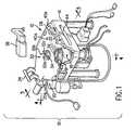
- a semiconductor processing system 10in accordance with one embodiment of the present invention includes an enclosure assembly 12 formed from a process-compatible material, such as aluminum or anodized aluminum.
- Enclosure assembly 12includes a housing 14 , defining a processing chamber 16 with an opening 18 , and a vacuum lid assembly 20 .
- Vacuum lid assembly 20is pivotally coupled to housing 14 via a hinge 22 to selectively cover opening 18 .
- a handle 24is attached to vacuum lid assembly 20 , opposite to hinge 22 . Handle 24 facilitates moving vacuum lid assembly 20 between opened and closed positions. In the opened position, opening 18 is exposed, allowing access to processing chamber 16 . In the closed position, vacuum lid assembly 20 covers opening 18 , forming a fluid-tight seal therewith. In this manner, a vacuum formed in chamber 16 maintains vacuum lid assembly 20 against housing 14 .
- Hinge 22includes a locking ratchet mechanism 28 to prevent vacuum lid assembly 20 from unintentionally moving into the closed position.
- Vacuum lid assembly 20includes a process fluid injection assembly 30 to deliver reactive and carrier fluids into processing chamber 16 , discussed more fully below.
- fluid injection assembly 30includes a plurality of high-flow-velocity valves, 32 a , 32 b and 32 c , a W-seal manifold 34 , a baffle plate 36 and a support 20 a .
- Valves, 32 a , 32 b and 32 c , W-seal manifold 34 , and baffle plate 36are mounted to support 20 a , discussed more fully below.
- a remote plasma source 38attached to support 20 a is a remote plasma source 38 that is placed in fluid communication with processing chamber 16 through radical input port 40 a in support 20 a .
- An intake port 40 bformed in support 20 a , is in fluid communication with remote plasma source 38 .
- Remote plasma sourceis a compact system that includes well-known subsystems. These subsystems include a microwave generator (not shown), in electrical communication with a plasma applicator (not shown), an autotuner (not shown), and an isolator (not shown). Wave-guides, shown for the sake of simplicity as 38 a , are coupled between the aforementioned subsystems.
- An intake conduit 38 bis in fluid communication with intake port 40 b .
- An intake line(not shown) extends through housing 14 and is in fluid communication with intake port 40 b to place a supply of etching fluids (not shown) in fluid communication with remote plasma source 38 .
- An exit port 38 cwhich is in fluid communication with wave-guide 38 a , is selectively placed in fluid communication with input port 40 a via an isolation valve 38 d.
- a slit valve opening 44is present in housing 14 , as well as a vacuum lock door (not shown). Slit valve opening 44 allows transfer of a wafer (not shown) between processing chamber 16 and the exterior of system 10 . Any conventional wafer transfer assembly (not shown) may achieve the aforementioned transfer.
- An example of a conventional robotic wafer transfer assemblyis described in commonly assigned U.S. Pat. No. 4,951,601 to Maydan, the complete disclosure of which is incorporated herein by reference.
- a heater/lift assembly 46that includes a wafer support pedestal 48 connected to a support shaft 48 a .
- Support pedestal 48is positioned between shaft 48 a and vacuum lid assembly 20 , when vacuum lid assembly 20 is in the closed position.
- Support shaft 48 aextends from wafer support pedestal 48 away from vacuum lid assembly 20 through an orifice 51 formed in housing 14 .
- Heater lift assembly 46is adapted to be controllably moved so as to vary the distance between support pedestal 48 and vacuum lid assembly 20 .
- a sensor(not shown) provides information concerning the position of support pedestal 48 within processing chamber 16 .
- An example of a lifting mechanism for support pedestal 48is described in detail in U.S. Pat. No. 5,951,776 to Selyutin et al., entitled “Self-Aligning Lift Mechanism”, which is assigned to the assignee of the present invention and incorporated by reference herein.
- Support pedestal 48may be maintained within a desired process temperature range employing an embedded thermocouple 50 to monitor the temperature thereof in a conventional manner. For example, the measured temperature may be used in a feedback loop to control the electrical current applied to heater element 51 by a heat exchange system 52 .
- support pedestal 48may be heated using radiant heat (not shown).
- Support pedestal 48may be formed from any process-compatible material, including aluminum nitride and aluminum oxide (Al 2 O 3 or alumina) and may also be configured to hold a substrate thereon employing a vacuum, i.e. support pedestal 48 may be a vacuum chuck. To that end, support pedestal 48 may include a plurality of vacuum holes 49 that are placed in fluid communication with a vacuum source, such as pump system 64 via vacuum tube 49 a.
- a liner assemblyis disposed in processing chamber 16 and includes a cylindrical portion 54 and a planar portion 56 .
- Cylindrical portion 54 and a planar portion 56may be formed from any suitable material such as aluminum, ceramic and the like. Cylindrical portion 54 surrounds support pedestal 48 .
- Planar portion 56extends transversely to cylindrical portion 54 and is disposed against a surface 14 a of processing chamber 16 disposed opposite to lid assembly 20 .
- Liner assemblydefines a chamber purge channel 58 between surface housing 14 and both cylindrical portion 54 and planar portion 56 . Specifically, a first portion of purge channel 58 is defined between surface 14 a and planar portion 56 .
- a second portion of purge channel 58is defined between surface 14 b and cylindrical portion 54 , with surface 14 b extending extends transversely to surface 14 a .
- the second portion of chamber purge channel 58places the first portion in fluid communication with a pump channel 60 that extends circumferentially about cylindrical portion 54 of liner assembly.
- Attached to a portion of housing 14 disposed opposite to lid assembly 20is a bellows 55 forming a fluid-tight void 57 , as is well known in the semiconductor processing art.
- void 57is filled with an inert, or purge fluid, such as argon.
- Purge channelis placed in fluid communication with void 57 and, therefore, the purge fluid therein, via a through-bore 61 .
- Through-bore 61extends through a portion of housing 14 , disposed opposite to vacuum lid assembly 20 .
- purge fluid in void 57may flow through purge channel 58 to reduce, if not, prevent accumulation of residue on surfaces 14 a and 14 b .
- Accumulation of residue on support pedestal 48 and on planar portion 56is reduced, if not prevented, by purge fluid flowing into processing chamber 16 through orifice 51 .
- Pump plate 62Disposed between pump channel 60 and lid assembly 20 is a pump plate 62 that includes a plurality of apertures, one of which is shown as 62 a .
- Pump plate 62controls the amount of flow between processing chamber 16 and pump channel 60 .
- the size and number and position of aperturesare established to achieve uniform flow over support pedestal 48 .
- the flow within processing chamber 16is provided by a pump system 64 .
- Pump system 64is in fluid communication with processing chamber 16 via an outlet line 66 and pump channel 60 .
- a plurality of supplies of process fluids, 68 a , 68 b and 68 care in fluid communication with one of valves 32 a , 32 b or 32 c through a sequence of conduits formed in housing 14 , lid assembly 20 , and W-seal manifold 34 , as discussed more fully below.
- a controller 70regulates the operations of the various components of system 10 .
- controller 70includes a processor 72 in data communication with memory, such as random access memory 74 and a hard disk drive 76 and is in signal communication with pump system 64 , heat exchange system 52 , and valves 32 a , 32 b and 32 c.
- system 10deposits electrically conductive or electrically insulative layers employing sequential deposition techniques, e.g., atomic layer deposition and atomic layer nucleation.
- the layersmay be deposited on the material from which a substrate 90 is fabricated, e.g., SiO 2 .
- the layermay be deposited on a layer previously formed on substrate 90 , e.g., titanium, titanium nitride and the like. Assuming that a layer is formed on substrate 90 , the initial surface presents an active ligand to the process region.
- a batch of a first processing fluidresults in a layer of A being deposited on substrate 90 having a surface of ligand a exposed to processing chamber 16 .
- a purge fluidenters processing chamber 16 to purge the fluid Aa x that remains therein.
- Bb ya second batch of processing fluid, is introduced, with y being an integer.
- the ligand present on substrate 90reacts with the b ligand and B atom, releasing molecules ab, Aa and Ab, that move away from substrate 90 and are subsequently pumped from processing chamber 16 .
- a surface comprising a monolayer of B atomsremains upon substrate 90 and is exposed to processing chamber 16 , shown in FIG. 7 .
- the processproceeds cycle after cycle, until the desired thickness for layer B is achieved.
- process fluid Aa xis B 2 H 6 gas and processing fluid Bb y is WF 6 gas
- two purge fluidsare employed: Ar gas and N 2 gas.
- the chamber pressureis in the range of 1-5 Torr, and pedestal 48 is heated in the range of 350° to 400° C.
- Each of the process fluidsis flowed into processing chamber 16 with a carrier fluid, which in this example were one of the purge fluids: WF 6 is introduced with Ar and B 2 H 6 is introduced with N 2 . It should be understood, however, that the purge fluid might differ from the carrier fluid, discussed more fully below.
- One cycle of the sequential deposition technique in accordance with the present inventionincludes flowing the purge fluid, N 2 , into processing chamber 16 during time t 1 , before B 2 H 6 is flowed into processing chamber 16 .
- the process fluid B 2 H 6is flowed into processing chamber 16 along with a carrier fluid, which in this example is N 2 .
- a carrier fluidwhich in this example is N 2 .
- the flow of N 2continues during time t 3 , purging processing chamber 16 of B 2 H 6 .
- processing chamber 16is pumped so as to remove all process fluids.
- the carrier fluid Aris introduced during time t 5 , after which time the process fluid WF 6 is introduced into processing chamber 16 , along with the carrier fluid Ar during time t 6 .
- the flow of Arcontinues during time t 7 .
- processing chamber 16is pumped so as to remove all process fluids therein, during time t 8 , thereby concluding one cycle of the sequential deposition technique in accordance with the present invention. This sequence of cycles is repeated until the layer being formed thereby has desired characteristics, such as thickness, conductivity and the like. It can be seen that the time required during each period t 1 -t 8 greatly affects the throughput of system 10 .
- the lid assembly 20 and injection assembly 30are configured to minimize the time required to inject process fluids into processing chamber 16 and disperse the fluids over the process region proximate to support pedestal 48 .
- lid assembly 20includes a support 20 a , high-flow-velocity valves, 32 a , 32 b and 32 c , W-seal manifold 34 , and baffle plate 36 .
- Valves 32 a , 32 b and 32 care surface mount electronically controlled valves that are available from Fujikin of Japan as part number FR-21-6.35 UGF-APD.
- Each of valves 32 a , 32 b and 32 cinclude an input port 80 and an output port 82 .
- Support 20 aincludes first and second opposed surfaces 20 b and 20 c , with a recessed region 20 d disposed in first surface 20 b .
- Recessed region 20 dincludes a sidewall 20 e that extends from first surface 20 b toward second surface 20 c , terminating in a recessed surface 20 f .
- Each of a plurality of pairs of fluid transfer holes 92 , 94 and 96includes a borehole, 92 a , 94 a and 96 a that extends between recessed surface 20 f and second surface 20 c .
- Also included with each pair of fluid transfer holes 92 , 94 and 96is an inlet passage 92 b , 94 b and 96 b.
- W-seal manifold 34is formed from a more durable material than assembly 12 .
- W-seal manifold 34may be fabricated from stainless steel and includes a plurality of pairs of fluid transfer channels 102 , 104 and 106 extending between opposed surfaces 34 a and 34 b .
- Each of the pairs of fluid transfer channels 102 , 104 and 106includes an injection channel, shown as 102 a , 104 a and 106 a , respectively.
- Also included with each of the pairs of fluid transfer channels 102 , 104 and 106is a reception channel, shown as 102 b , 104 b and 106 b , respectively.
- Baffle plate 36includes first and second opposed sides 36 a and 36 b .
- First side 36 ahas a recessed area 36 c .
- Recessed area 36 cincludes a sidewall 36 d that extends from first side 36 a toward second side 36 c , terminating in a nadir region that includes a throughway 36 e extending between the nadir region and second surface 36 b , defining an annular nadir surface 36 f .
- An annular protrusion 36 gextends from first side 36 a and surrounds recessed area 36 c . Spaced-apart from annular protrusion 36 g are a plurality of bulwarks 36 h that also extend from first side 36 a .
- Each of the plurality of bulwarksincludes a through-bore 36 i adapted to receive a fastener (not shown) to couple baffle plate 36 to support 20 a .
- W-seal manifold 34is coupled to support 20 a via fasteners (not shown) extending through bores (not shown), and valves 32 a , 32 b and 32 c are fastened to W-seal manifold 34 in a similar manner.
- W-seal manifold 34Upon being attached to support 20 a , W-seal manifold 34 is disposed within recessed region 20 d with surface 34 b resting against recessed surface 20 f forming a fluid-tight seal therewith. Fluid transfer channels 102 , 104 and 106 on W-seal manifold 34 are arranged to superimpose fluid transfer holes 92 , 94 and 96 and have a cross-sectional area that is coextensive therewith. In this manner, transfer channels 102 , 104 and 106 are coaxial with fluid transfer holes 92 , 94 and 96 .
- Output port 82 of each of valves 32 a , 32 b and 32 csuperimposes one of injection channels 102 a , 104 a and 106 a and, therefore, one of boreholes, 92 a , 94 a and 96 a .
- Output port 82has a cross-sectional area that is coextensive with the cross-sectional area of valve 32 a , 32 b and 32 c it superimposes.
- Input port 80 of each of valves 32 a , 32 b and 32 csuperimposes one of reception channels 102 a , 104 a and 106 a and, therefore, one of an inlet passage 92 b , 94 b and 96 b .
- Input port 80has a cross-sectional area that is coextensive with the cross-sectional area of valves 32 a , 32 b and 32 c it superimposes.
- Each of injection channels 92 a , 94 a and 96 asuperimposes with annular nadir surface 36 f.
- each of inlet passages 92 b , 94 b and 96 bis in fluid communication with supplies of process fluids 68 a , 68 b and 68 c via a fluid transfer channel that extends through support 20 a , and a fluid feed-through that extends through housing 14 .
- inlet passage 96 bis in fluid communication with fluid transfer channel 110 .
- Fluid transfer channel 110is connected to fluid feed-through 112 .
- fluid feed-through 112is in fluid communication with one of supplies 68 a , 68 b and 68 c through one of supply lines 69 a , 69 b and 69 c , respectively.
- fluid transfer channel 110 , and fluid feed-through 112define a fluid input path.
- each of inlet passages 92 b , 94 b and 96 bare connected to an input path that differs from the input path connected to the remaining inlet passages 92 b , 94 b and 96 b .
- each of supplies of process fluids 68 a , 68 b and 68 cis uniquely associated with one of valves 32 a , 32 b and 32 c , through differing feed-throughs (not shown).
- valve 32 ca flow of process fluids into processing chamber 16 is discussed below with respect to valve 32 c for ease of discussion and should be understood to apply to the two remaining valves 32 a and 32 b .
- Lid assembly 20is configured to minimize the time required to inject process fluids into processing chamber 16 .
- valve 32 cselectively allows fluid to flow between input port 80 and output port 82 .
- the pressure of fluid in input port 80 , before activation of valve 32 cmay be as high as 200 Torr, referred to as an up-stream pressure.
- fluidis transferred to output port 82 at a pressure of 200 Torr and drops rapidly, in a fraction of a second, to a pressure of as low as 2 Torr, referred to as a down-stream pressure.
- the difference in up-stream and down-stream pressuresresults in process fluids travel over path p 1 along a first direction d 1 and exiting borehole 96 a at a great velocity, up to 300 meters/second.
- Annular nadir surface 36 freduces the velocity of the process fluids traveling through processing chamber 16 , before the process fluids reach support pedestal 48 .
- process fluidsimpact with annular nadir surface 36 f , and annular nadir surface 36 f disperses these process fluids to travel in a plane p 2 that extends transversely to direction d 1 .
- the direction that the of process fluids travelis changed and the velocity of the same reduced before reaching support pedestal 48 .
- Changing the velocity and direction of process fluids exiting borehole 96 aovercomes a problem identified with implementation of valves 32 a , 32 b and 32 c . It was found that process fluids exiting borehole 96 a and passing directly through throughway 36 e to impinge upon a substrate (not shown) caused a film formed on there to have non-uniform thickness.
- the area of a film that is superimposed by the borehole 96 awould be thinner than the remaining areas of a film.
- Thisis believed to be, in part, to a thermal gradient that is created on the substrate (not shown).
- the thermal gradientis believed to result in the high velocity flow of process fluids impacting upon localized regions (not shown) of the substrate (note shown). These regions (not shown) have a lower temperature than the remaining regions (not shown) of the substrate (not shown), resulting in a lower deposition in these regions (not shown).
- the process fluidsare dispersed and slowed by annular nadir surface 36 f .
- a pressure differential present between sides 36 a and 36 bcauses the dispersed fluid to flow toward a common region of baffle plate 36 , such as recessed region 36 c . Thereafter, the process fluids once again travel along direction d 1 through throughway 36 e and along path p 3 .
- throughway 36 eAfter exiting throughway 36 e , the process fluids flow away from throughway 36 e and travel substantially parallel while the same impinges upon the entire area of a substrate (not shown) mounted atop of support pedestal 48 .
- throughway 36 eis radially and symmetrically disposed about an axis that is centered with respect to support pedestal 48 , and the area of baffle plate 36 is substantially coextensive with the area of support pedestal 48 .
- Providing recessed region 20 dfacilitates high-speed deposition of process fluids by shortening the distance between output port 82 and baffle plate 36 .
- Mounting of valves 32 a , 32 b and 32 cis achieved by bolting the same to lid assembly 20 .
- one embodiment of the present inventionincludes directly mounting valves 32 a , 32 b and 32 c to support 20 a , this configuration was found to be undesirable.
- Support 20 ais manufactured from aluminum or other lightweight material that is unsuitable for affixing valves 32 a , 32 b and 32 c thereto.
- W-seal manifold 34is provided.
- W-seal manifoldis manufactured from a more durable material, such as stainless steel.
- W-seal manifold 34increased the distance between output port 80 and baffle plate 36 by a magnitude equal, at least, to a length of injection channels 102 a , 104 a and 106 a .
- Recessed region 20 dis formed in support 20 a to compensate for the increased distance.
- W-seal manifold 34fits within recessed region 20 d , which reduces the aforementioned increase in distance between output port 80 and baffle plate 36 that results from the introduction of W-seal manifold 34 .
- baffle plate 136is identical to baffle plate 36 , excepting for the omission of annular protrusion 36 g and bulwarks 36 h . More specifically, surface 136 a is substantially planar so that the entire area thereof rests against support 20 a when coupled thereto. Baffle plate 36 , however, has attendant advantages by the presence of annular protrusion 36 g and bulwarks 36 h . With the configuration of baffle plate 36 , only annular protrusion 36 g and bulwarks 36 h are in contact with support 20 a when coupled thereto.
- the remaining regions of surface 36 aare spaced-apart from support 20 a , which facilitates removal of deposition residue from baffle plate 36 during a plasma clean process employing remote plasma source 38 .
- Thisis due, it is believed, by limiting thermal conduction between baffle plate 36 and support 20 a to annular protrusion 36 g and bulwarks 36 h . In this manner, the temperature of baffle plate 36 is maintained at a sufficiently high magnitude to remove most, if not all, residue therefrom by employing standard remote plasma clean techniques.
- Coolant channels 20 g in lid assembly 20 and a coolant channel 14 c in housing 14shown more clearly in FIG. 4 .
- Coolant channels 20 g and 14 care in fluid communication with a coolant manifold 14 d , which is connected to a supply (not shown) of a suitable coolant.
- an exemplary method of introducing processing fluids into semiconductor processing chamber 16includes injecting a process fluid into said processing chamber 16 over a path p 1 in a first direction d 1 toward support pedestal 48 , defining a flow of fluid at step 200 .
- a dispersed flowis formed from the flow of fluid by dispersing the same to propagate away from the path p 1 and over a plane p 2 that extends transversely to the first direction d 1 .
- the dispersed flowis moved toward a common region, such as throughway 36 d , in processing chamber 16 , disposed proximate to the path p 1 to form an accumulated flow of process fluid.
- the accumulated flowis directed along a second path p 3 , spaced-apart from the first path, along the first direction d 1 .
- the accumulated flowis radiated away from the common region at it travels toward support pedestal 48 , shown by arrows 37 .
- an interface between a user and controller 70may be via a visual display.
- one or more monitors 339 a and 339 bmay be employed.
- One monitor 339 amay be mounted in a clean room wall 340 having one or more systems 310 and 311 .
- the remaining monitor 339 bmay be mounted behind wall 340 for service personnel.
- Monitors 339 a and 339 bmay simultaneously display the same information.
- Communication with controller 70may be achieved with a light pen associated with each of monitors 339 a and 139 b .
- a light pen 341 afacilitates communication with controller 70 through monitor 339 a
- a light pen 341 bfacilitates communication with controller 70 through monitor 339 b .
- a light sensor in the tip of light pens 341 a and 341 bdetects light emitted by CRT display in response to a user pointing the same to an area of the display screen.
- the touched areachanges color, or a new menu or screen is displayed, confirming communication between the light pen and the display screen.
- Other devices, such as a keyboard, mouse, or other pointing or communication devicemay be used instead of or in addition to light pens 341 a and 341 b to allow the user to communicate with controller 70 .
- a computer program having sets of instructionscontrols the various subsystems of system 10 .
- the computer program codemay be written in any conventional computer readable programming language: for example, 68000 assembly language, C, C++, Pascal, Fortran and the like.
- Suitable program codeis entered into a single file or multiple files using a conventional text editor and stored or embodied in a computer-readable medium, such as memory 74 of controller 70 . If the entered code text is a high level language, the code is compiled.
- the resultant compiler codeis then linked with an object code of precompiled Windows® library routines. To execute the linked and compiled object code the system user invokes the object code, causing controller 70 to load the code in memory 74 from, for example, hard disk drive 76 . Controller 70 then reads and executes the code to perform the tasks identified in the program.
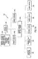
- FIGS. 13 and 14an illustrative block diagram of the hierarchical control structure of the system control software is shown including a computer program 342 that a user may access using a light pen interface.
- a usermay enter a process set number and system number into a process selector subroutine 343 in response to menus or screens displayed one or more of monitors 339 a and 339 b .
- Predefined set numbersidentifies the process sets, which are predetermined sets of process parameters necessary to carry out specified processes.
- Process selector subroutine 343identifies (i) the desired system 310 and 311 , and (ii) the desired set of process parameters needed to operate systems 310 and 311 for performing the desired process.
- Process parameters for performing a specific processrelate to process conditions such as process fluid composition and flow rates, pressure, plasma conditions such as high- and low-frequency RF power levels and the high and low RF frequencies (and in addition, microwave generator power levels for embodiments equipped with remote microwave plasma systems), and cooling fluid pressure.
- Process selector subroutine 343controls what type of process (deposition, substrate cleaning, chamber cleaning, chamber gettering, reflowing) is performed at an appropriate time. In some embodiments, there may be more than one process selector subroutine.
- a process sequencer subroutine 344comprises program code for accepting the identified system 310 and 311 and set of process parameters from chamber selector subroutine 343 , and for controlling operation of systems 310 and 311 .
- Multiple userscan enter process set numbers and system numbers, or a single user can enter multiple process set numbers and system numbers, so sequencer subroutine 344 operates to schedule the selected processes in the desired sequence.
- sequencer subroutine 344includes program code to perform the steps of (i) monitoring the operation of systems 310 and 311 to determine whether systems 310 and 311 are being used, (ii) determining what processes are being carried out in systems 310 and 311 , and (iii) executing the desired process based on availability of a system and the type of process to be carried out.
- sequencer subroutine 344may be designed to take into consideration the present condition of the system 310 and 311 being used in comparison with the desired process conditions for a selected process, or the “age” of each particular user-entered request, or any other relevant factor a system programmer desires to include for determining scheduling priorities.
- sequencer subroutine 344determines which system 310 and 311 and process set combination will be executed next, sequencer subroutine 344 initiates execution of the process set by passing the particular process set parameters to a chamber manager subroutine 345 a-c that controls multiple processing tasks according to the process set determined by sequencer subroutine 344 .
- chamber manager subroutine 345 bcomprises program code for controlling operations in systems 310 and 311 .
- Chamber manager subroutine 345 balso controls execution of various system component subroutines that controls operation of the system components necessary to carry out the selected process set.
- chamber component subroutinesare substrate positioning subroutine 346 , process fluid control subroutine 348 , pressure control subroutine 350 , heater control subroutine 352 , and plasma control subroutine 354 .
- some embodimentsinclude all of the above subroutines, while other embodiments may include only some of the subroutines.
- system control subroutinescan be included depending on what processes are to be performed in systems 310 and 311 .
- chamber manager subroutine 345 bselectively schedules or calls the system component subroutines in accordance with the particular process set being executed.
- Chamber manager subroutine 345 bschedules the system component subroutines much like sequencer subroutine 344 schedules which of systems 310 and 311 and process set is to be executed next.
- chamber manager subroutine 345 bincludes steps of monitoring the various system components, determining which components need to be operated based on the process parameters for the process set to be executed, and initiating execution of a system component subroutine responsive to the monitoring and determining steps.
- substrate positioning subroutine 346comprises program code for controlling system components that are used to load the substrate (not shown) onto support pedestal 48 and, optionally, to lift the substrate (not shown) to a desired height in processing chamber 16 to control the spacing between the substrate (not shown) and baffle plate 36 .
- heater/lift assembly 46is lowered to receive the substrate (not shown) on support pedestal 48 , and then is placed to the desired position.
- substrate positioning subroutine 346controls movement of heater/lift assembly 46 and support pedestal 48 in response to process set parameters related to the support height that are transferred from chamber manager subroutine 345 b.
- Process fluid control subroutine 348has program code for controlling process fluid composition and flow rates.
- Process fluid control subroutine 348controls the open/close position of the safety shut-off valves (not shown), and also ramps up/down the mass flow controllers (not shown) to obtain the desired fluid flow rate.
- Process fluid control subroutine 348is invoked by chamber manager subroutine 345 b , as are all system component subroutines, and receives subroutine process parameters related to the desired fluid flow rates from the chamber manager.
- process fluid control subroutine 348operates by activating valves 32 a , 32 b and 32 c to allow process fluids to traverse fluid supply lines 69 a , 69 b and 69 c , without the need for either (i) reading mass flow controllers, (ii) comparing the readings to the desired flow rates or (iii) adjusting the flow rates of fluid supply lines 69 a , 69 b and 69 c as necessary.
- process fluid control subroutine 348includes steps for monitoring the fluid flow rates for unsafe rates, and activating the safety shut-off valves (not shown) when an unsafe condition is detected.
- Process fluid control subroutine 348also controls the fluid composition and introduction of clean fluids as well as for deposition fluids, depending on the desired process (clean or deposition or other) that is selected.
- Alternative embodimentscould have more than one process fluid control subroutine, each subroutine controlling a specific type of process or specific sets of fluid lines.
- process fluid control subroutine 348is programmed to include steps for flowing the inert fluid into processing chamber 16 for an amount of time necessary to stabilize the pressure in processing chamber 16 , and then the steps described above would be carried out. Additionally, when a process fluid is to be vaporized from a liquid precursor, process fluid control subroutine 348 would be written to include steps for bubbling a delivery fluid, such as helium, through the liquid precursor in a bubbler assembly (not shown), or for introducing a carrier fluid, such as helium, to a liquid injection system.
- a delivery fluidsuch as helium
- process fluid control subroutine 348regulates the flow of the delivery fluid, the pressure in the bubbler (not shown), and the bubbler temperature in order to obtain the desired process fluid flow rates.
- the desired process fluid flow ratesare transferred to process fluid control subroutine 348 as process parameters.
- process fluid control subroutine 348includes steps for obtaining the necessary delivery fluid flow rate, bubbler pressure, and bubbler temperature for the desired process fluid flow rate by accessing a stored table containing the necessary values for a given process fluid flow rate. Once the necessary values are obtained, the delivery fluid flow rate, bubbler pressure and bubbler temperature are monitored, compared to the necessary values and adjusted accordingly.
- Pressure control subroutine 350comprises program code for controlling the pressure in the processing chamber 16 by regulating, inter alia, the aperture size of the throttle valve that is included in pump system 64 .
- the aperture size of the throttle valveis set to control the chamber pressure at a desired level in relation to the total process fluid flow, the size of processing chamber 16 , and the pumping set-point pressure for pump system 64 .
- pressure control subroutine 350is invoked, the desired or target pressure level is received as a parameter from chamber manager subroutine 345 b .
- Pressure control subroutine 350measures the pressure in processing chamber 16 by reading one or more conventional pressure manometers connected to processing chamber 16 , comparing the measure value(s) to the target pressure, obtaining PID (proportional, integral, and differential) values corresponding to the target pressure from a stored pressure table, and adjusting the throttle valve according to the PID values obtained from the pressure table.
- pressure control subroutine 350can be written to open or close the throttle valve (not shown) to a particular aperture size to regulate the pumping capacity in processing chamber 16 to the desired level.
- Heater control subroutine 352comprises program code to control operation of heat exchange system 52 and, therefore, the temperature of heater/lift assembly 46 .
- Plasma control subroutine 354comprises program code to control operation of remote plasma source 38 . Like the previously described system component subroutines, plasma control subroutine 354 is invoked by chamber manager subroutine 345 b.
Landscapes
- Chemical & Material Sciences (AREA)
- Engineering & Computer Science (AREA)
- General Chemical & Material Sciences (AREA)
- Chemical Kinetics & Catalysis (AREA)
- Materials Engineering (AREA)
- Mechanical Engineering (AREA)
- Metallurgy (AREA)
- Organic Chemistry (AREA)
- Physics & Mathematics (AREA)
- Condensed Matter Physics & Semiconductors (AREA)
- General Physics & Mathematics (AREA)
- Manufacturing & Machinery (AREA)
- Computer Hardware Design (AREA)
- Microelectronics & Electronic Packaging (AREA)
- Power Engineering (AREA)
- Chemical Vapour Deposition (AREA)
Abstract
Description
1. Field of the Invention
This invention relates to semiconductor processing. More particularly, this invention relates to a processing system and method of distributing fluid therein to facilitate sequential deposition of films on a substrate.
2. Description of the Related Art
The semiconductor processing industry continues to strive for larger production yields while increasing the uniformity of layers deposited on substrates having increasingly larger surface areas. These same factors in combination with new materials also provide higher integration of circuits per unit area of the substrate. As circuit integration increases, the need for greater uniformity and process control regarding layer thickness rises. As a result, various technologies have been developed to deposit layers on substrates in a cost-effective manner, while maintaining control over the characteristics of the layer. Chemical Vapor Deposition (CVD) is a common deposition processes employed for depositing layers on a substrate. CVD is a flux-dependent deposition technique that requires precise control of the substrate temperature and precursors introduced into the processing chamber in order to produce a desired layer of uniform thickness. These requirements become more critical as substrate size increases, creating a need for more complexity in chamber design and fluid flow technique to maintain adequate uniformity.
A variant of CVD that demonstrates superior step coverage is a sequential deposition technique known as Atomic Layer Deposition (ALD). ALD has steps of chemisorption that deposit monolayers of reactive precursor molecules on a substrate surface. To that end, a pulse of a first reactive precursor is introduced into a processing chamber to deposit a first monolayer of molecules on a substrate disposed in the processing chamber. A pulse of a second reactive precursor is introduced into the processing chamber to form an additional monolayer of molecules adjacent to the first monolayer of molecules. In this manner, a layer is formed on a substrate by alternatingly pulsing an appropriate reactive precursor into a deposition chamber. Each injection of a reactive precursor is separated by an inert fluid purge to provide a new atomic layer additive to previous deposited layers to form a uniform layer on the substrate. The cycle is repeated to form the layer to a desired thickness. A drawback with ALD techniques is that the deposition rate is much lower than typical CVD techniques.
A need exists, therefore, to reduce the time required to deposit films employing sequential deposition techniques.
Provided is a lid for a semiconductor system, an exemplary embodiment of which includes a support having opposed first and second opposed surfaces, with valve coupled to the first surface. A baffle plate is mounted to the second surface. The valve is coupled to the support to direct a flow of fluid along a path in an original direction and at an injection velocity. The baffle plate is disposed in the path to disperse the flow of fluid in a plane extending transversely to the original direction.
FIG. 1 is a simplified plan view of a plasma-based semiconductor processing system in accordance with one embodiment of the present invention;
FIG. 2 is a partial top-down view of a remote plasma source mounted to a support shown above in FIG. 1;
FIG. 3 is a cross-sectional view of the remote plasma source mounted to a support that is shown above in FIG. 2, taken alonglines 3—3;
FIG. 4 is a detailed cut-away perspective view of a processing chamber shown above in FIG. 1, taken alonglines 4—4;
FIG. 5 is a detailed cross-sectional view of a processing chamber, shown above in FIG. 1 taken alonglines 5—5 connected to various subsystems associated with system;
FIG. 6 is a schematic view showing deposition of a first molecule onto a substrate during sequential deposition;
FIG. 7 is a schematic view showing deposition of second molecule onto a substrate during sequential deposition to form a film layer;
FIG. 8 is a graphical representation showing the concentration of gases introduced into the processing chamber shown above in FIGS. 1,4-5, and the relative time in which the gases are present in the processing chamber;
FIG. 9 is an exploded perspective view of a lid assembly discussed above with respect to FIGS. 1-5;
FIG. 10 is a detailed cross-section view of a portion of the lid assembly shown above in FIG. 9;
FIG. 11 is a perspective view of an alternate embodiment of a baffle plate shown above in FIG. 10;
FIG. 12 is a flow diagram showing a method to flow process fluids into the process chamber in accordance with an embodiment of the present invention;
FIG. 13 is a perspective view of a processing environment in which the processing system, shown above in FIGS. 1,4-5, may be employed; and
FIG. 14 is a block diagram showing the hierarchical control structure of system control software employed to control the processing system, discussed above with respect to FIGS. 1,4-5 and13.
Referring to FIG. 1, asemiconductor processing system 10 in accordance with one embodiment of the present invention includes anenclosure assembly 12 formed from a process-compatible material, such as aluminum or anodized aluminum.Enclosure assembly 12 includes ahousing 14, defining aprocessing chamber 16 with anopening 18, and avacuum lid assembly 20.Vacuum lid assembly 20 is pivotally coupled tohousing 14 via ahinge 22 to selectively coveropening 18. Ahandle 24 is attached tovacuum lid assembly 20, opposite to hinge22.Handle 24 facilitates movingvacuum lid assembly 20 between opened and closed positions. In the opened position,opening 18 is exposed, allowing access toprocessing chamber 16. In the closed position,vacuum lid assembly 20 covers opening18, forming a fluid-tight seal therewith. In this manner, a vacuum formed inchamber 16 maintainsvacuum lid assembly 20 againsthousing 14. Hinge22, however, includes alocking ratchet mechanism 28 to preventvacuum lid assembly 20 from unintentionally moving into the closed position.
Referring to FIGS. 1,2 and3, attached to support20ais aremote plasma source 38 that is placed in fluid communication withprocessing chamber 16 throughradical input port 40ainsupport 20a. Anintake port 40b, formed insupport 20a, is in fluid communication withremote plasma source 38. Remote plasma source is a compact system that includes well-known subsystems. These subsystems include a microwave generator (not shown), in electrical communication with a plasma applicator (not shown), an autotuner (not shown), and an isolator (not shown). Wave-guides, shown for the sake of simplicity as38a, are coupled between the aforementioned subsystems. Anintake conduit 38bis in fluid communication withintake port 40b. An intake line (not shown) extends throughhousing 14 and is in fluid communication withintake port 40bto place a supply of etching fluids (not shown) in fluid communication withremote plasma source 38. Anexit port 38c, which is in fluid communication with wave-guide 38a, is selectively placed in fluid communication withinput port 40avia anisolation valve 38d.
To facilitate access toprocessing chamber 16, without compromising the fluid-tight seal betweenvacuum lid assembly 20 andhousing 14, aslit valve opening 44 is present inhousing 14, as well as a vacuum lock door (not shown).Slit valve opening 44 allows transfer of a wafer (not shown) betweenprocessing chamber 16 and the exterior ofsystem 10. Any conventional wafer transfer assembly (not shown) may achieve the aforementioned transfer. An example of a conventional robotic wafer transfer assembly is described in commonly assigned U.S. Pat. No. 4,951,601 to Maydan, the complete disclosure of which is incorporated herein by reference.
Referring to FIGS. 4 and 5, disposed withinprocessing chamber 16 is a heater/lift assembly 46 that includes awafer support pedestal 48 connected to a support shaft48a.Support pedestal 48 is positioned between shaft48aandvacuum lid assembly 20, whenvacuum lid assembly 20 is in the closed position. Support shaft48aextends fromwafer support pedestal 48 away fromvacuum lid assembly 20 through anorifice 51 formed inhousing 14.Heater lift assembly 46 is adapted to be controllably moved so as to vary the distance betweensupport pedestal 48 andvacuum lid assembly 20. A sensor (not shown) provides information concerning the position ofsupport pedestal 48 withinprocessing chamber 16. An example of a lifting mechanism forsupport pedestal 48 is described in detail in U.S. Pat. No. 5,951,776 to Selyutin et al., entitled “Self-Aligning Lift Mechanism”, which is assigned to the assignee of the present invention and incorporated by reference herein.
A liner assembly is disposed in processingchamber 16 and includes acylindrical portion 54 and aplanar portion 56.Cylindrical portion 54 and aplanar portion 56 may be formed from any suitable material such as aluminum, ceramic and the like.Cylindrical portion 54 surroundssupport pedestal 48.Planar portion 56 extends transversely tocylindrical portion 54 and is disposed against asurface 14aofprocessing chamber 16 disposed opposite tolid assembly 20. Liner assembly defines achamber purge channel 58 betweensurface housing 14 and bothcylindrical portion 54 andplanar portion 56. Specifically, a first portion ofpurge channel 58 is defined betweensurface 14aandplanar portion 56. A second portion ofpurge channel 58 is defined betweensurface 14bandcylindrical portion 54, withsurface 14bextending extends transversely to surface14a. The second portion ofchamber purge channel 58 places the first portion in fluid communication with apump channel 60 that extends circumferentially aboutcylindrical portion 54 of liner assembly. Attached to a portion ofhousing 14 disposed opposite tolid assembly 20 is a bellows55 forming a fluid-tight void 57, as is well known in the semiconductor processing art. Typically, void57 is filled with an inert, or purge fluid, such as argon. Purge channel is placed in fluid communication withvoid 57 and, therefore, the purge fluid therein, via a through-bore 61. Through-bore 61 extends through a portion ofhousing 14, disposed opposite to vacuumlid assembly 20. In this manner, purge fluid invoid 57 may flow throughpurge channel 58 to reduce, if not, prevent accumulation of residue onsurfaces support pedestal 48 and onplanar portion 56 is reduced, if not prevented, by purge fluid flowing intoprocessing chamber 16 throughorifice 51.
Disposed betweenpump channel 60 andlid assembly 20 is apump plate 62 that includes a plurality of apertures, one of which is shown as62a.Pump plate 62 controls the amount of flow betweenprocessing chamber 16 andpump channel 60. The size and number and position of apertures are established to achieve uniform flow oversupport pedestal 48. The flow withinprocessing chamber 16 is provided by apump system 64.Pump system 64 is in fluid communication withprocessing chamber 16 via anoutlet line 66 andpump channel 60. A plurality of supplies of process fluids,68a,68band68care in fluid communication with one ofvalves housing 14,lid assembly 20, and W-seal manifold 34, as discussed more fully below. Acontroller 70 regulates the operations of the various components ofsystem 10. To that end,controller 70 includes aprocessor 72 in data communication with memory, such asrandom access memory 74 and ahard disk drive 76 and is in signal communication withpump system 64,heat exchange system 52, andvalves
Referring to FIGS. 1,6, and7, during operation,system 10 deposits electrically conductive or electrically insulative layers employing sequential deposition techniques, e.g., atomic layer deposition and atomic layer nucleation. Depending on the specific stage of processing, the layers may be deposited on the material from which asubstrate 90 is fabricated, e.g., SiO2. Alternatively, the layer may be deposited on a layer previously formed onsubstrate 90, e.g., titanium, titanium nitride and the like. Assuming that a layer is formed onsubstrate 90, the initial surface presents an active ligand to the process region. A batch of a first processing fluid, in this case Aax, where x is an integer, results in a layer of A being deposited onsubstrate 90 having a surface of ligand a exposed to processingchamber 16. Thereafter, a purge fluid enters processingchamber 16 to purge the fluid Aaxthat remains therein. After purging Aaxfrom processingchamber 16, a second batch of processing fluid, Bby, is introduced, with y being an integer. The ligand present onsubstrate 90 reacts with the b ligand and B atom, releasing molecules ab, Aa and Ab, that move away fromsubstrate 90 and are subsequently pumped from processingchamber 16. In this manner, a surface comprising a monolayer of B atoms remains uponsubstrate 90 and is exposed to processingchamber 16, shown in FIG.7. The process proceeds cycle after cycle, until the desired thickness for layer B is achieved.
Referring to both FIGS. 4,6, and8, although any type of process fluid may be employed, an example is discussed in which process fluid Aaxis B2H6gas and processing fluid Bbyis WF6gas, and two purge fluids are employed: Ar gas and N2gas. The chamber pressure is in the range of 1-5 Torr, andpedestal 48 is heated in the range of 350° to 400° C. Each of the process fluids is flowed intoprocessing chamber 16 with a carrier fluid, which in this example were one of the purge fluids: WF6is introduced with Ar and B2H6is introduced with N2. It should be understood, however, that the purge fluid might differ from the carrier fluid, discussed more fully below.
One cycle of the sequential deposition technique in accordance with the present invention includes flowing the purge fluid, N2, intoprocessing chamber 16 during time t1, before B2H6is flowed intoprocessing chamber 16. During time t2, the process fluid B2H6is flowed intoprocessing chamber 16 along with a carrier fluid, which in this example is N2. After the flow of B2H6terminates, the flow of N2continues during time t3, purgingprocessing chamber 16 of B2H6. During time t4, processingchamber 16 is pumped so as to remove all process fluids. After pumping of processingchamber 16, the carrier fluid Ar is introduced during time t5, after which time the process fluid WF6is introduced intoprocessing chamber 16, along with the carrier fluid Ar during time t6. After the flow of WF6intoprocessing chamber 16 terminates, the flow of Ar continues during time t7. Thereafter, processingchamber 16 is pumped so as to remove all process fluids therein, during time t8, thereby concluding one cycle of the sequential deposition technique in accordance with the present invention. This sequence of cycles is repeated until the layer being formed thereby has desired characteristics, such as thickness, conductivity and the like. It can be seen that the time required during each period t1-t8greatly affects the throughput ofsystem 10. To maximize the throughput, thelid assembly 20 andinjection assembly 30 are configured to minimize the time required to inject process fluids intoprocessing chamber 16 and disperse the fluids over the process region proximate to supportpedestal 48.
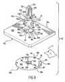
Referring to FIG. 9, as discussed above,lid assembly 20 includes asupport 20a, high-flow-velocity valves,32a,32band32c, W-seal manifold 34, and baffleplate 36.Valves valves input port 80 and anoutput port 82.Support 20aincludes first and secondopposed surfaces region 20ddisposed infirst surface 20b. Recessedregion 20dincludes asidewall 20ethat extends fromfirst surface 20btowardsecond surface 20c, terminating in a recessed surface20f. Each of a plurality of pairs of fluid transfer holes92,94 and96 includes a borehole,92a,94aand96athat extends between recessed surface20fandsecond surface 20c. Also included with each pair of fluid transfer holes92,94 and96 is aninlet passage
W-seal manifold 34 is formed from a more durable material thanassembly 12. For example, W-seal manifold 34 may be fabricated from stainless steel and includes a plurality of pairs offluid transfer channels opposed surfaces fluid transfer channels fluid transfer channels
Upon being attached to support20a, W-seal manifold 34 is disposed within recessedregion 20dwithsurface 34bresting against recessed surface20fforming a fluid-tight seal therewith.Fluid transfer channels seal manifold 34 are arranged to superimpose fluid transfer holes92,94 and96 and have a cross-sectional area that is coextensive therewith. In this manner,transfer channels Output port 82 of each ofvalves injection channels Output port 82 has a cross-sectional area that is coextensive with the cross-sectional area ofvalve Input port 80 of each ofvalves reception channels inlet passage Input port 80 has a cross-sectional area that is coextensive with the cross-sectional area ofvalves injection channels annular nadir surface 36f.
Referring to FIGS. 4,5, and9, each ofinlet passages support 20a, and a fluid feed-through that extends throughhousing 14. As shown,inlet passage 96bis in fluid communication withfluid transfer channel 110.Fluid transfer channel 110 is connected to fluid feed-through112. Although not shown, fluid feed-through112 is in fluid communication with one of supplies68a,68band68cthrough one ofsupply lines fluid transfer channel 110, and fluid feed-through112 define a fluid input path. It should be understood that each ofinlet passages inlet passages valves
Referring to FIGS. 1,9 and10, a flow of process fluids intoprocessing chamber 16 is discussed below with respect tovalve 32cfor ease of discussion and should be understood to apply to the two remainingvalves Lid assembly 20 is configured to minimize the time required to inject process fluids intoprocessing chamber 16. To that end,valve 32cselectively allows fluid to flow betweeninput port 80 andoutput port 82. The pressure of fluid ininput port 80, before activation ofvalve 32cmay be as high as 200 Torr, referred to as an up-stream pressure. After activation ofvalve 32c, fluid is transferred tooutput port 82 at a pressure of 200 Torr and drops rapidly, in a fraction of a second, to a pressure of as low as 2 Torr, referred to as a down-stream pressure. The difference in up-stream and down-stream pressures results in process fluids travel over path p1along a first direction d1and exitingborehole 96aat a great velocity, up to 300 meters/second.Annular nadir surface 36freduces the velocity of the process fluids traveling throughprocessing chamber 16, before the process fluids reachsupport pedestal 48. Specifically, process fluids impact withannular nadir surface 36f, andannular nadir surface 36fdisperses these process fluids to travel in a plane p2that extends transversely to direction d1. In this manner, the direction that the of process fluids travel is changed and the velocity of the same reduced before reachingsupport pedestal 48. Changing the velocity and direction of processfluids exiting borehole 96aovercomes a problem identified with implementation ofvalves fluids exiting borehole 96aand passing directly throughthroughway 36eto impinge upon a substrate (not shown) caused a film formed on there to have non-uniform thickness. Specifically, the area of a film that is superimposed by the borehole96awould be thinner than the remaining areas of a film. This is believed to be, in part, to a thermal gradient that is created on the substrate (not shown). The thermal gradient is believed to result in the high velocity flow of process fluids impacting upon localized regions (not shown) of the substrate (note shown). These regions (not shown) have a lower temperature than the remaining regions (not shown) of the substrate (not shown), resulting in a lower deposition in these regions (not shown). To avoid the aforementioned temperature gradient, and the aforementioned thinning effect, the process fluids are dispersed and slowed byannular nadir surface 36f. Thereafter, a pressure differential present betweensides baffle plate 36, such as recessedregion 36c. Thereafter, the process fluids once again travel along direction d1throughthroughway 36eand along path p3.
After exitingthroughway 36e, the process fluids flow away fromthroughway 36eand travel substantially parallel while the same impinges upon the entire area of a substrate (not shown) mounted atop ofsupport pedestal 48. To that end,throughway 36eis radially and symmetrically disposed about an axis that is centered with respect to supportpedestal 48, and the area ofbaffle plate 36 is substantially coextensive with the area ofsupport pedestal 48.
Providing recessedregion 20dfacilitates high-speed deposition of process fluids by shortening the distance betweenoutput port 82 andbaffle plate 36. Mounting ofvalves lid assembly 20. Although one embodiment of the present invention includes directly mountingvalves Support 20ais manufactured from aluminum or other lightweight material that is unsuitable for affixingvalves seal manifold 34 is provided. W-seal manifold is manufactured from a more durable material, such as stainless steel. It was recognized that the introduction of W-seal manifold 34 increased the distance betweenoutput port 80 andbaffle plate 36 by a magnitude equal, at least, to a length ofinjection channels region 20dis formed insupport 20ato compensate for the increased distance. Specifically, W-seal manifold 34 fits within recessedregion 20d, which reduces the aforementioned increase in distance betweenoutput port 80 andbaffle plate 36 that results from the introduction of W-seal manifold 34.
Referring to FIGS. 4,9, and11, another embodiment ofbaffle plate 36 is shown asbaffle plate 136.Baffle plate 136 is identical to baffleplate 36, excepting for the omission ofannular protrusion 36gandbulwarks 36h. More specifically,surface 136ais substantially planar so that the entire area thereof rests againstsupport 20awhen coupled thereto.Baffle plate 36, however, has attendant advantages by the presence ofannular protrusion 36gandbulwarks 36h. With the configuration ofbaffle plate 36, onlyannular protrusion 36gandbulwarks 36hare in contact withsupport 20awhen coupled thereto. The remaining regions ofsurface 36aare spaced-apart fromsupport 20a, which facilitates removal of deposition residue frombaffle plate 36 during a plasma clean process employingremote plasma source 38. This is due, it is believed, by limiting thermal conduction betweenbaffle plate 36 andsupport 20atoannular protrusion 36gandbulwarks 36h. In this manner, the temperature ofbaffle plate 36 is maintained at a sufficiently high magnitude to remove most, if not all, residue therefrom by employing standard remote plasma clean techniques.
Further temperature control ofsystem 10 may be achieved bycoolant channels 20ginlid assembly 20 and acoolant channel 14cinhousing 14, shown more clearly in FIG.4.Coolant channels coolant manifold 14d, which is connected to a supply (not shown) of a suitable coolant.
Referring to FIGS. 5,10 and12, an exemplary method of introducing processing fluids intosemiconductor processing chamber 16 includes injecting a process fluid into saidprocessing chamber 16 over a path p1in a first direction d1towardsupport pedestal 48, defining a flow of fluid atstep 200. Atstep 202, a dispersed flow is formed from the flow of fluid by dispersing the same to propagate away from the path p1and over a plane p2that extends transversely to the first direction d1. Atstep 204, the dispersed flow is moved toward a common region, such asthroughway 36d, in processingchamber 16, disposed proximate to the path p1to form an accumulated flow of process fluid. Atstep 206, the accumulated flow is directed along a second path p3, spaced-apart from the first path, along the first direction d1. Atstep 208, the accumulated flow is radiated away from the common region at it travels towardsupport pedestal 48, shown by arrows37.
Referring to FIGS. 5 and 13 an interface between a user andcontroller 70 may be via a visual display. To that end, one ormore monitors monitor 339amay be mounted in aclean room wall 340 having one ormore systems monitor 339bmay be mounted behindwall 340 for service personnel.Monitors controller 70 may be achieved with a light pen associated with each ofmonitors 339aand139b. For example, a light pen341 a facilitates communication withcontroller 70 throughmonitor 339a, and alight pen 341bfacilitates communication withcontroller 70 throughmonitor 339b. A light sensor in the tip oflight pens 341aand341bdetects light emitted by CRT display in response to a user pointing the same to an area of the display screen. The touched area changes color, or a new menu or screen is displayed, confirming communication between the light pen and the display screen. Other devices, such as a keyboard, mouse, or other pointing or communication device may be used instead of or in addition tolight pens 341aand341bto allow the user to communicate withcontroller 70.
As discussed above, a computer program having sets of instructions controls the various subsystems ofsystem 10. The computer program code may be written in any conventional computer readable programming language: for example, 68000 assembly language, C, C++, Pascal, Fortran and the like. Suitable program code is entered into a single file or multiple files using a conventional text editor and stored or embodied in a computer-readable medium, such asmemory 74 ofcontroller 70. If the entered code text is a high level language, the code is compiled. The resultant compiler code is then linked with an object code of precompiled Windows® library routines. To execute the linked and compiled object code the system user invokes the object code, causingcontroller 70 to load the code inmemory 74 from, for example,hard disk drive 76.Controller 70 then reads and executes the code to perform the tasks identified in the program.
Referring to both FIGS. 13 and 14 an illustrative block diagram of the hierarchical control structure of the system control software is shown including acomputer program 342 that a user may access using a light pen interface. For example, a user may enter a process set number and system number into aprocess selector subroutine 343 in response to menus or screens displayed one or more ofmonitors Process selector subroutine 343 identifies (i) the desiredsystem systems Process selector subroutine 343 controls what type of process (deposition, substrate cleaning, chamber cleaning, chamber gettering, reflowing) is performed at an appropriate time. In some embodiments, there may be more than one process selector subroutine.
Aprocess sequencer subroutine 344 comprises program code for accepting the identifiedsystem chamber selector subroutine 343, and for controlling operation ofsystems sequencer subroutine 344 operates to schedule the selected processes in the desired sequence. Preferably,sequencer subroutine 344 includes program code to perform the steps of (i) monitoring the operation ofsystems systems systems monitoring systems sequencer subroutine 344 may be designed to take into consideration the present condition of thesystem
Oncesequencer subroutine 344 determines whichsystem sequencer subroutine 344 initiates execution of the process set by passing the particular process set parameters to a chamber manager subroutine345a-cthat controls multiple processing tasks according to the process set determined bysequencer subroutine 344. For example,chamber manager subroutine 345bcomprises program code for controlling operations insystems Chamber manager subroutine 345balso controls execution of various system component subroutines that controls operation of the system components necessary to carry out the selected process set. Examples of chamber component subroutines aresubstrate positioning subroutine 346, processfluid control subroutine 348,pressure control subroutine 350,heater control subroutine 352, andplasma control subroutine 354. Depending on the specific configuration of the system, some embodiments include all of the above subroutines, while other embodiments may include only some of the subroutines. Those having ordinary skill in the art would readily recognize that other system control subroutines can be included depending on what processes are to be performed insystems chamber manager subroutine 345bselectively schedules or calls the system component subroutines in accordance with the particular process set being executed.Chamber manager subroutine 345bschedules the system component subroutines much likesequencer subroutine 344 schedules which ofsystems chamber manager subroutine 345bincludes steps of monitoring the various system components, determining which components need to be operated based on the process parameters for the process set to be executed, and initiating execution of a system component subroutine responsive to the monitoring and determining steps.
Referring to both FIGS. 5 and 14,substrate positioning subroutine 346 comprises program code for controlling system components that are used to load the substrate (not shown) ontosupport pedestal 48 and, optionally, to lift the substrate (not shown) to a desired height in processingchamber 16 to control the spacing between the substrate (not shown) andbaffle plate 36. When a substrate is loaded intoprocessing chamber 16, heater/lift assembly 46 is lowered to receive the substrate (not shown) onsupport pedestal 48, and then is placed to the desired position. In operation,substrate positioning subroutine 346 controls movement of heater/lift assembly 46 andsupport pedestal 48 in response to process set parameters related to the support height that are transferred fromchamber manager subroutine 345b.
Processfluid control subroutine 348 has program code for controlling process fluid composition and flow rates. Processfluid control subroutine 348 controls the open/close position of the safety shut-off valves (not shown), and also ramps up/down the mass flow controllers (not shown) to obtain the desired fluid flow rate. Processfluid control subroutine 348 is invoked bychamber manager subroutine 345b, as are all system component subroutines, and receives subroutine process parameters related to the desired fluid flow rates from the chamber manager. Typically, processfluid control subroutine 348 operates by activatingvalves fluid supply lines fluid supply lines fluid control subroutine 348 includes steps for monitoring the fluid flow rates for unsafe rates, and activating the safety shut-off valves (not shown) when an unsafe condition is detected. Processfluid control subroutine 348 also controls the fluid composition and introduction of clean fluids as well as for deposition fluids, depending on the desired process (clean or deposition or other) that is selected. Alternative embodiments could have more than one process fluid control subroutine, each subroutine controlling a specific type of process or specific sets of fluid lines.
As discussed above, some processes have an inert fluid such as nitrogen, N2, or argon, Ar, is flowed intoprocessing chamber 16 to stabilize the pressure in processingchamber 16 before reactive process fluids are introduced. For these processes, processfluid control subroutine 348 is programmed to include steps for flowing the inert fluid intoprocessing chamber 16 for an amount of time necessary to stabilize the pressure in processingchamber 16, and then the steps described above would be carried out. Additionally, when a process fluid is to be vaporized from a liquid precursor, processfluid control subroutine 348 would be written to include steps for bubbling a delivery fluid, such as helium, through the liquid precursor in a bubbler assembly (not shown), or for introducing a carrier fluid, such as helium, to a liquid injection system. When a bubbler is used for this type of process, processfluid control subroutine 348 regulates the flow of the delivery fluid, the pressure in the bubbler (not shown), and the bubbler temperature in order to obtain the desired process fluid flow rates. As discussed above, the desired process fluid flow rates are transferred to processfluid control subroutine 348 as process parameters. Furthermore, processfluid control subroutine 348 includes steps for obtaining the necessary delivery fluid flow rate, bubbler pressure, and bubbler temperature for the desired process fluid flow rate by accessing a stored table containing the necessary values for a given process fluid flow rate. Once the necessary values are obtained, the delivery fluid flow rate, bubbler pressure and bubbler temperature are monitored, compared to the necessary values and adjusted accordingly.
Although the invention has been described in terms of specific embodiments, one skilled in the art will recognize that various modifications may be made that are within the scope of the present invention. For example, although three valves are shown, any number of valves may be provided, depending upon the number of differing process fluids employed to deposit a film. Therefore, the scope of the invention should not be based upon the foregoing description. Rather, the scope of the invention should be determined based upon the claims recited herein, including the full scope of equivalents thereof.
Claims (28)
1. A lid assembly for a semiconductor processing system, comprising:
a support having first and second opposed surfaces;
a valve coupled to said first surface; and
a baffle plate mounted to said second surface and having a throughway disposed in a recessed area of the baffle plate, with said valve coupled to said support to direct a flow of fluid through a borehole in the support along a path in an original direction and at an injection velocity and said baffle plate being disposed in said path to disperse said flow of fluid in a plane extending at least partially transversely to said original direction.
2. The assembly as recited inclaim 1 wherein the bore hole extends between said first and second opposed surfaces and said baffle plate further includes first and second opposed sides, with said first side having the recessed area, wherein the recessed area extends from said first side and terminates in a nadir region having the throughway formed therein, wherein the throughway extends between said nadir region and said second surface, defining an annular nadir surface, with said borehole superimposing said annular nadir surface.
3. The assembly as recited inclaim 1 wherein said baffle plate further includes first and second opposed sides, an annular protrusion and a plurality of bulwarks spaced apart from said annular protrusion, with said protrusion and said plurality of bulwarks extending from said first side and contacting said support, with the remaining regions of said first side being spaced-apart from the support.
4. The assembly as recited inclaim 1 wherein said support further includes a recessed region disposed in said first surface, said recessed region including a sidewall extending from said first surface, toward said second surface and terminating in a recessed surface with a borehole extending between said recessed surface and said second surface, said baffle plate further including first and second opposed sides, with said first side having the recessed area, wherein the recessed area extends from said first side and terminates in a nadir region having the throughway formed therein, wherein the throughway extends between said nadir region and said second surface, defining an annular nadir surface, with said borehole superimposing said annular nadir surface.
5. The assembly as recited inclaim 4 further including a W-seal manifold disposed within said recessed region, between said valve and said recessed surface, said manifold having an injection channel and a reception channel, with said injection channel being axially aligned and in fluid communication with both said output port and said borehole and having a cross-sectional area coextensive therewith, with said reception channel being in fluid communication with said input port.
6. The assembly as recited inclaim 1 further including a W-seal manifold mounted between said valve and said support, said manifold having an injection channel and a reception channel, with said injection channel being axially aligned and in fluid communication with both said output port and said borehole and having a cross-sectional area coextensive therewith, with said reception channel being in fluid communication with said input port.
7. The assembly as recited inclaim 1 wherein said through-way is disposed radially and symmetrically about an axis, with said support further including a radical through-port extending between said first and second opposed surfaces and spaced apart from said axis.
8. A lid assembly for a semiconductor processing system, comprising:
a support having first and second opposed surfaces with a borehole extending therebetween;
a valve coupled to said first surface and in fluid communication with said borehole; and
a baffle plate mounted to said second surface, said baffle plate including first and second opposed sides, with a recessed area extending from said first side and terminating in a nadir region having a throughway formed therein extending between said nadir region and said second surface, defining an annular nadir surface, with said borehole superimposing said annular nadir surface.
9. The assembly as recited inclaim 8 further including an additional valve, with said valve and said additional valve defining a plurality of valves, and wherein said support further includes an additional borehole, with said borehole and said additional borehole defining a plurality of boreholes, with each of said plurality of valves being in fluid communication with one of said plurality of boreholes.
10. The assembly as recited inclaim 9 further including a W-seal manifold disposed between said plurality of valves and said support, wherein each of said plurality of valves includes an input port and an output port and said W-seal manifold includes a plurality of pairs of fluid transfer channels, with each pair of fluid transfer channels including an injection channel and a reception channel, with each injection channel of said plurality of pairs of fluid transfer channels being axially aligned and in fluid communication with both said output port and one of said plurality of boreholes and having a cross-sectional area coextensive therewith, with said reception channel being in fluid communication with said input port.
11. The assembly as recited inclaim 10 wherein said support further includes a recessed region disposed in said first surface, said recessed region including a sidewall extending from said first surface, toward said second surface and terminating in a recessed surface with said plurality of boreholes extending between said recessed surface and said second surface, with said W-seal manifold being disposed within said recessed region.
12. The assembly as recited inclaim 11 said baffle plate further includes an annular protrusion surrounding said recessed area and a plurality of bulwarks spaced-apart from said annular protrusion, with said protrusion and said plurality of bulwarks extending from said first side and contacting said support, with the remaining regions of said first side being spaced-apart from said support.
13. The assembly as recited inclaim 12 wherein said through-way is disposed radially and symmetrically about an axis, with said support further including a radical through-port extending between said first and second opposed surfaces and spaced apart from said axis.
14. A lid assembly for semiconductor processing system, comprising:
means for forming a first path over which process fluids travel along a first direction, defining a flow of fluid;
means, connected to said means for forming, for dispersing said flow of fluid to propagate over a plane away from said path, with said plane extending transversely to said first direction, defining a dispersed flow; and
means, connected to said means for forming, for creating a second path, disposed spaced apart from said first path to move said dispersed flow along said first direction.
15. The assembly as recited inclaim 14 wherein said means for forming a first path includes a support having first and second opposed surfaces with a plurality of boreholes extending therebetween, and plurality of valves coupled to said first surface, each of which includes an output port in fluid communication with one of said plurality of boreholes.
16. The assembly as recited inclaim 15 wherein said means for forming a first path further includes a W-seal manifold disposed between said plurality of valves and said support, with said W-seal manifold including a plurality of injection channels each of which is axially aligned and in fluid communication with both said output port and one of said plurality of boreholes and having a cross-sectional area coextensive therewith.
17. The assembly as recited inclaim 16 wherein said support further includes a recessed region disposed in said first surface, said recessed region including a sidewall extending from said first surface, toward said second surface and terminating in a recessed surface with said plurality of boreholes extending between said recessed surface and said second surface, with said W-seal manifold being disposed within said recessed region.
18. The assembly as recited inclaim 14 wherein said means for dispersing said flow of fluid includes a baffle plate mounted to said second surface, said baffle plate including first and second opposed sides with said first side being superimposed by said plurality of boreholes.
19. The assembly as recited inclaim 18 wherein said baffle plate further includes first and second opposed sides with a throughway extending therebetween, with said means for creating a second path further including positioning said throughway to lie outside of said path.
20. The assembly as recited inclaim 19 wherein said baffle plate further includes a recessed area extending from said first side and terminating in a nadir region having said throughway formed therein extending between said nadir region and said second surface, defining an annular nadir surface, with said plurality of boreholes superimposing said annular nadir surface.
21. The assembly as recited inclaim 20 wherein said baffle plate further includes an annular protrusion surrounding said recessed area and a plurality of bulwarks spaced-apart from said annular protrusion, with said protrusion and said plurality of bulwarks extending from said first side and contacting said means for forming a first path, with the remaining regions of said first side being spaced-apart from said means for forming a first path.
22. A lid assembly for a semiconductor processing system, comprising:
a support having first and second opposed surfaces and a plurality of holes disposed therethrough;
a plurality of valves coupled to the first surface of the support, wherein each valve of the plurality of valves has an outlet that is connected to one of the plurality of holes;
a baffle plate coupled to the second surface of the support, wherein the baffle plate has one throughway that provides a single outlet into the semiconductor processing system for all of the outlets of the plurality of valves.
23. The lid assembly ofclaim 22 , wherein the throughway in the baffle plate is in a recessed area of the baffle plate.
24. The lid assembly ofclaim 22 , wherein each of the valve outlets superimposes the throughway of the baffle plate.
25. The lid assembly ofclaim 22 , wherein the baffle plate is coupled to the second surface of the support via protrusions on the baffle plate such that the remaining regions of the baffle plate are spaced apart from the second surface of the support.
26. The lid assembly ofclaim 22 , wherein the plurality of holes extend from a recessed region in the first surface of the support to the second surface of the support.
27. The lid assembly ofclaim 26 , wherein a W-seal manifold is disposed in the recessed region.
28. The lid assembly ofclaim 22 , wherein a W-seal manifold is mounted between the plurality of valves and the support.
Priority Applications (2)
| Application Number | Priority Date | Filing Date | Title |
|---|---|---|---|
| US09/798,251US6660126B2 (en) | 2001-03-02 | 2001-03-02 | Lid assembly for a processing system to facilitate sequential deposition techniques |
| PCT/US2002/005647WO2002070779A1 (en) | 2001-03-02 | 2002-02-25 | Apparatus and method for sequential deposition of films |
Applications Claiming Priority (1)
| Application Number | Priority Date | Filing Date | Title |
|---|---|---|---|
| US09/798,251US6660126B2 (en) | 2001-03-02 | 2001-03-02 | Lid assembly for a processing system to facilitate sequential deposition techniques |
Publications (2)
| Publication Number | Publication Date |
|---|---|
| US20020121342A1 US20020121342A1 (en) | 2002-09-05 |
| US6660126B2true US6660126B2 (en) | 2003-12-09 |
Family
ID=25172910
Family Applications (1)
| Application Number | Title | Priority Date | Filing Date |
|---|---|---|---|
| US09/798,251Expired - Fee RelatedUS6660126B2 (en) | 2001-03-02 | 2001-03-02 | Lid assembly for a processing system to facilitate sequential deposition techniques |
Country Status (1)
| Country | Link |
|---|---|
| US (1) | US6660126B2 (en) |
Cited By (67)
| Publication number | Priority date | Publication date | Assignee | Title |
|---|---|---|---|---|
| US20030010451A1 (en)* | 2001-07-16 | 2003-01-16 | Applied Materials, Inc. | Lid assembly for a processing system to facilitate sequential deposition techniques |
| US20030175423A1 (en)* | 2002-02-27 | 2003-09-18 | Annette Saenger | Method and device for depositing thin layers via ALD/CVD processes in combination with rapid thermal processes |
| US20040173308A1 (en)* | 2002-11-04 | 2004-09-09 | Schutte Christopher L. | Semiconductor wafer handler |
| US6831004B2 (en) | 2000-06-27 | 2004-12-14 | Applied Materials, Inc. | Formation of boride barrier layers using chemisorption techniques |
| US6838125B2 (en) | 2002-07-10 | 2005-01-04 | Applied Materials, Inc. | Method of film deposition using activated precursor gases |
| US20050014382A1 (en)* | 2003-07-16 | 2005-01-20 | Samsung Electronics Co., Ltd. | Etching apparatus and method |
| US20050100669A1 (en)* | 2003-11-12 | 2005-05-12 | Veeco Instruments, Inc. | Method and apparatus for fabricating a conformal thin film on a substrate |
| US6916398B2 (en) | 2001-10-26 | 2005-07-12 | Applied Materials, Inc. | Gas delivery apparatus and method for atomic layer deposition |
| US6936538B2 (en) | 2001-07-16 | 2005-08-30 | Applied Materials, Inc. | Method and apparatus for depositing tungsten after surface treatment to improve film characteristics |
| US6972267B2 (en) | 2002-03-04 | 2005-12-06 | Applied Materials, Inc. | Sequential deposition of tantalum nitride using a tantalum-containing precursor and a nitrogen-containing precursor |
| US20060021573A1 (en)* | 2004-06-28 | 2006-02-02 | Cambridge Nanotech Inc. | Vapor deposition systems and methods |
| US7037574B2 (en) | 2001-05-23 | 2006-05-02 | Veeco Instruments, Inc. | Atomic layer deposition for fabricating thin films |
| US7049226B2 (en) | 2001-09-26 | 2006-05-23 | Applied Materials, Inc. | Integration of ALD tantalum nitride for copper metallization |
| US7085616B2 (en) | 2001-07-27 | 2006-08-01 | Applied Materials, Inc. | Atomic layer deposition apparatus |
| US20060196418A1 (en)* | 2005-03-04 | 2006-09-07 | Picosun Oy | Apparatuses and methods for deposition of material on surfaces |
| US20060216548A1 (en)* | 2005-03-22 | 2006-09-28 | Ming Mao | Nanolaminate thin films and method for forming the same using atomic layer deposition |
| US7115499B2 (en) | 2002-02-26 | 2006-10-03 | Applied Materials, Inc. | Cyclical deposition of tungsten nitride for metal oxide gate electrode |
| US7115494B2 (en) | 2000-06-28 | 2006-10-03 | Applied Materials, Inc. | Method and system for controlling the presence of fluorine in refractory metal layers |
| US20060272577A1 (en)* | 2005-06-03 | 2006-12-07 | Ming Mao | Method and apparatus for decreasing deposition time of a thin film |
| US7175713B2 (en) | 2002-01-25 | 2007-02-13 | Applied Materials, Inc. | Apparatus for cyclical deposition of thin films |
| US7204886B2 (en) | 2002-11-14 | 2007-04-17 | Applied Materials, Inc. | Apparatus and method for hybrid chemical processing |
| US7211508B2 (en) | 2003-06-18 | 2007-05-01 | Applied Materials, Inc. | Atomic layer deposition of tantalum based barrier materials |
| US7220673B2 (en) | 2000-06-28 | 2007-05-22 | Applied Materials, Inc. | Method for depositing tungsten-containing layers by vapor deposition techniques |
| US7262133B2 (en) | 2003-01-07 | 2007-08-28 | Applied Materials, Inc. | Enhancement of copper line reliability using thin ALD tan film to cap the copper line |
| US7270709B2 (en) | 2002-07-17 | 2007-09-18 | Applied Materials, Inc. | Method and apparatus of generating PDMAT precursor |
| US7294208B2 (en) | 2002-07-29 | 2007-11-13 | Applied Materials, Inc. | Apparatus for providing gas to a processing chamber |
| US20080044573A1 (en)* | 2003-11-03 | 2008-02-21 | Applied Materials, Inc. | Rate control process for a precursor delivery system |
| US20080050932A1 (en)* | 2006-08-23 | 2008-02-28 | Applied Materials, Inc. | Overall defect reduction for PECVD films |
| US20080051018A1 (en)* | 2004-03-16 | 2008-02-28 | Texas Instruments Incorporated | Semiconductor Wafer Handler |
| US7342984B1 (en) | 2003-04-03 | 2008-03-11 | Zilog, Inc. | Counting clock cycles over the duration of a first character and using a remainder value to determine when to sample a bit of a second character |
| US7352048B2 (en) | 2001-09-26 | 2008-04-01 | Applied Materials, Inc. | Integration of barrier layer and seed layer |
| US7384867B2 (en) | 2001-07-16 | 2008-06-10 | Applied Materials, Inc. | Formation of composite tungsten films |
| US7402534B2 (en) | 2005-08-26 | 2008-07-22 | Applied Materials, Inc. | Pretreatment processes within a batch ALD reactor |
| US7405158B2 (en) | 2000-06-28 | 2008-07-29 | Applied Materials, Inc. | Methods for depositing tungsten layers employing atomic layer deposition techniques |
| US7416979B2 (en) | 2001-07-25 | 2008-08-26 | Applied Materials, Inc. | Deposition methods for barrier and tungsten materials |
| US7422637B2 (en) | 2002-10-09 | 2008-09-09 | Applied Materials, Inc. | Processing chamber configured for uniform gas flow |
| US7429402B2 (en) | 2004-12-10 | 2008-09-30 | Applied Materials, Inc. | Ruthenium as an underlayer for tungsten film deposition |
| US7464917B2 (en) | 2005-10-07 | 2008-12-16 | Appiled Materials, Inc. | Ampoule splash guard apparatus |
| US7470611B2 (en) | 1998-10-01 | 2008-12-30 | Applied Materials, Inc. | In situ deposition of a low K dielectric layer, barrier layer, etch stop, and anti-reflective coating for damascene application |
| US7473638B2 (en) | 2002-01-26 | 2009-01-06 | Applied Materials, Inc. | Plasma-enhanced cyclic layer deposition process for barrier layers |
| US7547952B2 (en) | 2003-04-04 | 2009-06-16 | Applied Materials, Inc. | Method for hafnium nitride deposition |
| US7601648B2 (en) | 2006-07-31 | 2009-10-13 | Applied Materials, Inc. | Method for fabricating an integrated gate dielectric layer for field effect transistors |
| US7611990B2 (en) | 2001-07-25 | 2009-11-03 | Applied Materials, Inc. | Deposition methods for barrier and tungsten materials |
| USD606952S1 (en)* | 2009-01-16 | 2009-12-29 | Asm Genitech Korea Ltd. | Plasma inducing plate for semiconductor deposition apparatus |
| US7682946B2 (en) | 2005-11-04 | 2010-03-23 | Applied Materials, Inc. | Apparatus and process for plasma-enhanced atomic layer deposition |
| US7695563B2 (en) | 2001-07-13 | 2010-04-13 | Applied Materials, Inc. | Pulsed deposition process for tungsten nucleation |
| US7732327B2 (en) | 2000-06-28 | 2010-06-08 | Applied Materials, Inc. | Vapor deposition of tungsten materials |
| US7775508B2 (en) | 2006-10-31 | 2010-08-17 | Applied Materials, Inc. | Ampoule for liquid draw and vapor draw with a continuous level sensor |
| US7780785B2 (en) | 2001-10-26 | 2010-08-24 | Applied Materials, Inc. | Gas delivery apparatus for atomic layer deposition |
| US7794544B2 (en) | 2004-05-12 | 2010-09-14 | Applied Materials, Inc. | Control of gas flow and delivery to suppress the formation of particles in an MOCVD/ALD system |
| US7798096B2 (en) | 2006-05-05 | 2010-09-21 | Applied Materials, Inc. | Plasma, UV and ion/neutral assisted ALD or CVD in a batch tool |
| US7867914B2 (en) | 2002-04-16 | 2011-01-11 | Applied Materials, Inc. | System and method for forming an integrated barrier layer |
| US7871470B2 (en) | 2003-03-12 | 2011-01-18 | Applied Materials, Inc. | Substrate support lift mechanism |
| US20110059259A1 (en)* | 2009-09-08 | 2011-03-10 | Universal Display Corporation | Method and System for High-Throughput Deposition of Patterned Organic Thin Films |
| US7964505B2 (en) | 2005-01-19 | 2011-06-21 | Applied Materials, Inc. | Atomic layer deposition of tungsten materials |
| US8075728B2 (en) | 2008-02-28 | 2011-12-13 | Applied Materials, Inc. | Gas flow equalizer plate suitable for use in a substrate process chamber |
| US8110489B2 (en) | 2001-07-25 | 2012-02-07 | Applied Materials, Inc. | Process for forming cobalt-containing materials |
| US8119210B2 (en) | 2004-05-21 | 2012-02-21 | Applied Materials, Inc. | Formation of a silicon oxynitride layer on a high-k dielectric material |
| US8146896B2 (en) | 2008-10-31 | 2012-04-03 | Applied Materials, Inc. | Chemical precursor ampoule for vapor deposition processes |
| US8187970B2 (en) | 2001-07-25 | 2012-05-29 | Applied Materials, Inc. | Process for forming cobalt and cobalt silicide materials in tungsten contact applications |
| US8323754B2 (en) | 2004-05-21 | 2012-12-04 | Applied Materials, Inc. | Stabilization of high-k dielectric materials |
| TWI383426B (en)* | 2004-04-12 | 2013-01-21 | Ulvac Inc | A method for forming a barrier film and a method for forming an electrode film |
| US8536071B2 (en) | 2009-04-10 | 2013-09-17 | Lam Research Corporation | Gasket with positioning feature for clamped monolithic showerhead electrode |
| US8821637B2 (en) | 2007-01-29 | 2014-09-02 | Applied Materials, Inc. | Temperature controlled lid assembly for tungsten nitride deposition |
| US9051641B2 (en) | 2001-07-25 | 2015-06-09 | Applied Materials, Inc. | Cobalt deposition on barrier surfaces |
| US9911579B2 (en)* | 2014-07-03 | 2018-03-06 | Applied Materials, Inc. | Showerhead having a detachable high resistivity gas distribution plate |
| US10651016B2 (en)* | 2017-03-15 | 2020-05-12 | Hermes-Epitek Corporation | Detachable gas injector used for semiconductor equipment |
Families Citing this family (9)
| Publication number | Priority date | Publication date | Assignee | Title |
|---|---|---|---|---|
| US6849545B2 (en) | 2001-06-20 | 2005-02-01 | Applied Materials, Inc. | System and method to form a composite film stack utilizing sequential deposition techniques |
| TW589684B (en)* | 2001-10-10 | 2004-06-01 | Applied Materials Inc | Method for depositing refractory metal layers employing sequential deposition techniques |
| US6998014B2 (en) | 2002-01-26 | 2006-02-14 | Applied Materials, Inc. | Apparatus and method for plasma assisted deposition |
| KR20080033406A (en)* | 2005-07-29 | 2008-04-16 | 에비자 테크놀로지, 인크. | Deposition apparatus for semiconductor processing |
| KR101046520B1 (en)* | 2007-09-07 | 2011-07-04 | 어플라이드 머티어리얼스, 인코포레이티드 | Source gas flow path control in pecvd system to control a by-product film deposition on inside chamber |
| JP5869899B2 (en)* | 2011-04-01 | 2016-02-24 | 株式会社日立国際電気 | Substrate processing apparatus, semiconductor device manufacturing method, substrate processing method, and susceptor cover |
| US8826857B2 (en)* | 2011-11-21 | 2014-09-09 | Lam Research Corporation | Plasma processing assemblies including hinge assemblies |
| JP5766647B2 (en)* | 2012-03-28 | 2015-08-19 | 東京エレクトロン株式会社 | Heat treatment system, heat treatment method, and program |
| US10435786B2 (en)* | 2014-09-10 | 2019-10-08 | Applied Materials, Inc. | Alignment systems employing actuators providing relative displacement between lid assemblies of process chambers and substrates, and related methods |
Citations (226)
| Publication number | Priority date | Publication date | Assignee | Title |
|---|---|---|---|---|
| US3603284A (en)* | 1970-01-02 | 1971-09-07 | Ibm | Vapor deposition apparatus |
| US4058430A (en) | 1974-11-29 | 1977-11-15 | Tuomo Suntola | Method for producing compound thin films |
| US4389973A (en) | 1980-03-18 | 1983-06-28 | Oy Lohja Ab | Apparatus for performing growth of compound thin films |
| US4413022A (en) | 1979-02-28 | 1983-11-01 | Canon Kabushiki Kaisha | Method for performing growth of compound thin films |
| US4486487A (en) | 1982-05-10 | 1984-12-04 | Oy Lohja Ab | Combination film, in particular for thin film electroluminescent structures |
| JPS6065712A (en) | 1983-09-20 | 1985-04-15 | Toshiba Corp | Method of forming silicon oxide film |
| US4718976A (en)* | 1982-03-31 | 1988-01-12 | Fujitsu Limited | Process and apparatus for plasma treatment |
| US4767494A (en) | 1986-07-04 | 1988-08-30 | Nippon Telegraph & Telephone Corporation | Preparation process of compound semiconductor |
| US4806321A (en) | 1984-07-26 | 1989-02-21 | Research Development Corporation Of Japan | Use of infrared radiation and an ellipsoidal reflection mirror |
| US4813846A (en) | 1987-02-13 | 1989-03-21 | Leybold-Heraeus Gmbh | Inserting device for vacuum apparatus |
| US4829022A (en) | 1985-12-09 | 1989-05-09 | Nippon Telegraph And Telephone Corporation | Method for forming thin films of compound semiconductors by flow rate modulation epitaxy |
| US4834831A (en) | 1986-09-08 | 1989-05-30 | Research Development Corporation Of Japan | Method for growing single crystal thin films of element semiconductor |
| US4838983A (en) | 1986-07-03 | 1989-06-13 | Emcore, Inc. | Gas treatment apparatus and method |
| US4838993A (en) | 1986-12-04 | 1989-06-13 | Seiko Instruments Inc. | Method of fabricating MOS field effect transistor |
| US4840921A (en) | 1987-07-01 | 1989-06-20 | Nec Corporation | Process for the growth of III-V group compound semiconductor crystal on a Si substrate |
| US4845049A (en) | 1987-03-27 | 1989-07-04 | Nec Corporation | Doping III-V compound semiconductor devices with group VI monolayers using ALE |
| FR2626110A1 (en) | 1988-01-19 | 1989-07-21 | Thomson Csf | Process for producing a layer of a superconductive material by epitaxy |
| US4859627A (en) | 1987-07-01 | 1989-08-22 | Nec Corporation | Group VI doping of III-V semiconductors during ALE |
| US4859625A (en) | 1986-11-22 | 1989-08-22 | Research Development Corporation of Japan, Junichi Nishizawa and Oki Electric Industry Co., Ltd. | Method for epitaxial growth of compound semiconductor using MOCVD with molecular layer epitaxy |
| US4861417A (en) | 1987-03-27 | 1989-08-29 | Fujitsu Limited | Method of growing group III-V compound semiconductor epitaxial layer |
| US4876218A (en) | 1987-09-29 | 1989-10-24 | Oy Nokia Ab | Method of growing GaAs films on Si or GaAs substrates using ale |
| EP0344352A1 (en) | 1988-06-03 | 1989-12-06 | International Business Machines Corporation | Method for making artificial layered high-Tc superconductors |
| US4917556A (en) | 1986-04-28 | 1990-04-17 | Varian Associates, Inc. | Modular wafer transport and processing system |
| US4927670A (en) | 1988-06-22 | 1990-05-22 | Georgia Tech Research Corporation | Chemical vapor deposition of mixed metal oxide coatings |
| US4931132A (en) | 1988-10-07 | 1990-06-05 | Bell Communications Research, Inc. | Optical control of deposition of crystal monolayers |
| US4951601A (en) | 1986-12-19 | 1990-08-28 | Applied Materials, Inc. | Multi-chamber integrated process system |
| US4960720A (en) | 1986-08-26 | 1990-10-02 | Masafumi Shimbo | Method of growing compound semiconductor thin film using multichamber smoothing process |
| US4975252A (en) | 1984-07-26 | 1990-12-04 | Junichi Nishizawa | Semiconductor crystal growth apparatus |
| US4977855A (en)* | 1987-01-29 | 1990-12-18 | Tadahiro Ohmi | Apparatus for forming film with surface reaction |
| US4993357A (en) | 1987-12-23 | 1991-02-19 | Cs Halbleiter -Und Solartechnologie Gmbh | Apparatus for atomic layer epitaxial growth |
| US5000113A (en) | 1986-12-19 | 1991-03-19 | Applied Materials, Inc. | Thermal CVD/PECVD reactor and use for thermal chemical vapor deposition of silicon dioxide and in-situ multi-step planarized process |
| US5013683A (en) | 1989-01-23 | 1991-05-07 | The Regents Of The University Of California | Method for growing tilted superlattices |
| EP0429270A2 (en) | 1989-11-20 | 1991-05-29 | Kokusai Electric Co., Ltd. | Continuous etching method and apparatus therefor |
| US5028565A (en) | 1989-08-25 | 1991-07-02 | Applied Materials, Inc. | Process for CVD deposition of tungsten layer on semiconductor wafer |
| WO1991010510A1 (en) | 1990-01-16 | 1991-07-25 | Neste Oy | Process and apparatus for preparing heterogeneous catalysts |
| EP0442490A1 (en) | 1990-02-14 | 1991-08-21 | Sumitomo Electric Industries, Ltd. | Method for producing single crystal boron nitride film |
| US5082798A (en) | 1990-04-18 | 1992-01-21 | Mitsubishi Denki Kabushiki Kaisha | Crystal growth method |
| US5085885A (en) | 1990-09-10 | 1992-02-04 | University Of Delaware | Plasma-induced, in-situ generation, transport and use or collection of reactive precursors |
| US5091320A (en) | 1990-06-15 | 1992-02-25 | Bell Communications Research, Inc. | Ellipsometric control of material growth |
| US5130269A (en) | 1988-04-27 | 1992-07-14 | Fujitsu Limited | Hetero-epitaxially grown compound semiconductor substrate and a method of growing the same |
| US5166092A (en) | 1988-01-28 | 1992-11-24 | Fujitsu Limited | Method of growing compound semiconductor epitaxial layer by atomic layer epitaxy |
| US5173474A (en) | 1990-04-18 | 1992-12-22 | Xerox Corporation | Silicon substrate having an epitaxial superconducting layer thereon and method of making same |
| WO1993002111A1 (en) | 1991-07-16 | 1993-02-04 | Neste Oy | Process for preparing a polymerization catalyst by vapourizing chromium acetylacetonate |
| US5186718A (en) | 1989-05-19 | 1993-02-16 | Applied Materials, Inc. | Staged-vacuum wafer processing system and method |
| US5205077A (en) | 1990-08-31 | 1993-04-27 | Peter Wolters Ag | Apparatus for controlling operation of a lapping, honing or polishing machine |
| US5225366A (en) | 1990-06-22 | 1993-07-06 | The United States Of America As Represented By The Secretary Of The Navy | Apparatus for and a method of growing thin films of elemental semiconductors |
| US5234561A (en) | 1988-08-25 | 1993-08-10 | Hauzer Industries Bv | Physical vapor deposition dual coating process |
| US5246536A (en) | 1986-09-08 | 1993-09-21 | Research Development Corporation Of Japan | Method for growing single crystal thin films of element semiconductor |
| US5250148A (en) | 1985-05-15 | 1993-10-05 | Research Development Corporation | Process for growing GaAs monocrystal film |
| US5254207A (en) | 1991-11-30 | 1993-10-19 | Research Development Corporation Of Japan | Method of epitaxially growing semiconductor crystal using light as a detector |
| US5256244A (en) | 1992-02-10 | 1993-10-26 | General Electric Company | Production of diffuse reflective coatings by atomic layer epitaxy |
| US5259881A (en) | 1991-05-17 | 1993-11-09 | Materials Research Corporation | Wafer processing cluster tool batch preheating and degassing apparatus |
| US5270247A (en) | 1991-07-12 | 1993-12-14 | Fujitsu Limited | Atomic layer epitaxy of compound semiconductor |
| FR2692597A1 (en) | 1992-06-18 | 1993-12-24 | Mikrokemia Oy | Method and apparatus for introducing liquid phase reagents into a chemical reactor, and application of a coating to a substrate for chemical vapor deposition. |
| US5278435A (en) | 1992-06-08 | 1994-01-11 | Apa Optics, Inc. | High responsivity ultraviolet gallium nitride detector |
| US5286296A (en) | 1991-01-10 | 1994-02-15 | Sony Corporation | Multi-chamber wafer process equipment having plural, physically communicating transfer means |
| US5290748A (en) | 1990-01-16 | 1994-03-01 | Neste Oy | Polymerization catalyst for olefines |
| US5294286A (en) | 1984-07-26 | 1994-03-15 | Research Development Corporation Of Japan | Process for forming a thin film of silicon |
| US5296403A (en) | 1990-01-31 | 1994-03-22 | Research Development Corp. Of Japan | Method of manufacturing a static induction field-effect transistor |
| US5311055A (en) | 1991-11-22 | 1994-05-10 | The United States Of America As Represented By The Secretary Of The Navy | Trenched bipolar transistor structures |
| US5316793A (en) | 1992-07-27 | 1994-05-31 | Texas Instruments Incorporated | Directed effusive beam atomic layer epitaxy system and method |
| US5316615A (en) | 1990-03-23 | 1994-05-31 | International Business Machines Corporation | Surfactant-enhanced epitaxy |
| US5330610A (en) | 1993-05-28 | 1994-07-19 | Martin Marietta Energy Systems, Inc. | Method of digital epilaxy by externally controlled closed-loop feedback |
| US5336324A (en) | 1991-12-04 | 1994-08-09 | Emcore Corporation | Apparatus for depositing a coating on a substrate |
| US5338389A (en) | 1990-01-19 | 1994-08-16 | Research Development Corporation Of Japan | Method of epitaxially growing compound crystal and doping method therein |
| US5348911A (en) | 1987-06-30 | 1994-09-20 | Aixtron Gmbh | Material-saving process for fabricating mixed crystals |
| US5374570A (en) | 1989-03-17 | 1994-12-20 | Fujitsu Limited | Method of manufacturing active matrix display device using insulation layer formed by the ale method |
| US5395791A (en) | 1992-05-22 | 1995-03-07 | Minnesota Mining And Manufacturing Company | Growth of II VI laser diodes with quantum wells by atomic layer epitaxy and migration enhanced epitaxy |
| US5438952A (en) | 1993-03-24 | 1995-08-08 | Fujitsu Limited | Method of growing a semiconductor layer and a fabrication method of a semiconductor device using such a semiconductor layer |
| US5441703A (en) | 1987-06-30 | 1995-08-15 | Aixtron Gmbh | Gas inlet for a plurality of reactant gases into reaction vessel |
| US5441568A (en)* | 1994-07-15 | 1995-08-15 | Applied Materials, Inc. | Exhaust baffle for uniform gas flow pattern |
| US5443647A (en) | 1993-04-28 | 1995-08-22 | The United States Of America As Represented By The Secretary Of The Army | Method and apparatus for depositing a refractory thin film by chemical vapor deposition |
| US5455072A (en) | 1992-11-18 | 1995-10-03 | Bension; Rouvain M. | Initiation and bonding of diamond and other thin films |
| US5458084A (en) | 1992-04-16 | 1995-10-17 | Moxtek, Inc. | X-ray wave diffraction optics constructed by atomic layer epitaxy |
| US5469806A (en) | 1992-08-21 | 1995-11-28 | Nec Corporation | Method for epitaxial growth of semiconductor crystal by using halogenide |
| US5480818A (en) | 1992-02-10 | 1996-01-02 | Fujitsu Limited | Method for forming a film and method for manufacturing a thin film transistor |
| US5483919A (en) | 1990-08-31 | 1996-01-16 | Nippon Telegraph And Telephone Corporation | Atomic layer epitaxy method and apparatus |
| US5494522A (en)* | 1993-03-17 | 1996-02-27 | Tokyo Electron Limited | Plasma process system and method |
| US5503875A (en) | 1993-03-18 | 1996-04-02 | Tokyo Electron Limited | Film forming method wherein a partial pressure of a reaction byproduct in a processing container is reduced temporarily |
| EP0709875A1 (en)* | 1994-10-26 | 1996-05-01 | Applied Materials, Inc. | A processing chamber gas distribution manifold |
| US5521126A (en) | 1993-06-25 | 1996-05-28 | Nec Corporation | Method of fabricating semiconductor devices |
| US5527733A (en) | 1989-07-27 | 1996-06-18 | Seiko Instruments Inc. | Impurity doping method with adsorbed diffusion source |
| WO1996018756A1 (en) | 1994-12-16 | 1996-06-20 | Nkt Research Center A/S | A PA-CVD PROCESS FOR DEPOSITION OF A SOLID METAL-CONTAINING FILM ONTO A SUBSTRATE CONTAINING AT LEAST 50 % of Fe or WC |
| US5532511A (en) | 1992-10-23 | 1996-07-02 | Research Development Corp. Of Japan | Semiconductor device comprising a highspeed static induction transistor |
| US5580380A (en) | 1991-12-20 | 1996-12-03 | North Carolina State University | Method for forming a diamond coated field emitter and device produced thereby |
| DE19627017A1 (en) | 1995-07-07 | 1997-01-09 | Toshiba Kawasaki Kk | Process for the selective deposition of a metal film |
| US5601651A (en) | 1992-09-17 | 1997-02-11 | Fujitsu Limited | Flow control valve for use in fabrication of semiconductor devices |
| US5609689A (en) | 1995-06-09 | 1997-03-11 | Tokyo Electron Limited | Vacuum process apparaus |
| US5616181A (en) | 1994-11-24 | 1997-04-01 | Mitsubishi Denki Kabushiki Kaisha | MBE apparatus and gas branch piping apparatus |
| EP0768702A1 (en) | 1995-10-16 | 1997-04-16 | Applied Materials, Inc. | Gas injection slit nozzle for a plasma process reactor |
| US5637530A (en) | 1991-09-09 | 1997-06-10 | U.S. Philips Corporation | II-VI compound semiconductor epitaxial layers having low defects, method for producing and devices utilizing same |
| US5641984A (en) | 1994-08-19 | 1997-06-24 | General Electric Company | Hermetically sealed radiation imager |
| US5644128A (en) | 1994-08-25 | 1997-07-01 | Ionwerks | Fast timing position sensitive detector |
| US5667592A (en) | 1996-04-16 | 1997-09-16 | Gasonics International | Process chamber sleeve with ring seals for isolating individual process modules in a common cluster |
| US5674786A (en) | 1993-01-28 | 1997-10-07 | Applied Materials, Inc. | Method of heating and cooling large area glass substrates |
| EP0799641A2 (en) | 1996-04-03 | 1997-10-08 | Mikrokemia Oy | Functional surfaces for chemical reactions and process for the preparation thereof |
| US5693139A (en) | 1984-07-26 | 1997-12-02 | Research Development Corporation Of Japan | Growth of doped semiconductor monolayers |
| US5695564A (en) | 1994-08-19 | 1997-12-09 | Tokyo Electron Limited | Semiconductor processing system |
| US5705224A (en) | 1991-03-20 | 1998-01-06 | Kokusai Electric Co., Ltd. | Vapor depositing method |
| US5711811A (en) | 1994-11-28 | 1998-01-27 | Mikrokemia Oy | Method and equipment for growing thin films |
| US5730802A (en) | 1994-05-20 | 1998-03-24 | Sharp Kabushiki Kaisha | Vapor growth apparatus and vapor growth method capable of growing good productivity |
| US5730801A (en) | 1994-08-23 | 1998-03-24 | Applied Materials, Inc. | Compartnetalized substrate processing chamber |
| US5747113A (en) | 1996-07-29 | 1998-05-05 | Tsai; Charles Su-Chang | Method of chemical vapor deposition for producing layer variation by planetary susceptor rotation |
| US5749974A (en) | 1994-07-15 | 1998-05-12 | Shin-Etsu Handotai Co., Ltd. | Method of chemical vapor deposition and reactor therefor |
| US5788799A (en) | 1996-06-11 | 1998-08-04 | Applied Materials, Inc. | Apparatus and method for cleaning of semiconductor process chamber surfaces |
| US5788447A (en) | 1995-08-05 | 1998-08-04 | Kokusai Electric Co., Ltd. | Substrate processing apparatus |
| US5796116A (en) | 1994-07-27 | 1998-08-18 | Sharp Kabushiki Kaisha | Thin-film semiconductor device including a semiconductor film with high field-effect mobility |
| US5801634A (en) | 1997-09-08 | 1998-09-01 | Sony Corporation | Signal tower controller |
| US5807792A (en) | 1996-12-18 | 1998-09-15 | Siemens Aktiengesellschaft | Uniform distribution of reactants in a device layer |
| US5830270A (en) | 1996-08-05 | 1998-11-03 | Lockheed Martin Energy Systems, Inc. | CaTiO3 Interfacial template structure on semiconductor-based material and the growth of electroceramic thin-films in the perovskite class |
| US5835677A (en) | 1996-10-03 | 1998-11-10 | Emcore Corporation | Liquid vaporizer system and method |
| US5851849A (en) | 1997-05-22 | 1998-12-22 | Lucent Technologies Inc. | Process for passivating semiconductor laser structures with severe steps in surface topography |
| US5856219A (en) | 1992-12-02 | 1999-01-05 | Matsushita Electric Industrial Co., Ltd. | Method of fabricating a high-density dynamic random-access memory |
| US5855675A (en) | 1997-03-03 | 1999-01-05 | Genus, Inc. | Multipurpose processing chamber for chemical vapor deposition processes |
| US5855680A (en) | 1994-11-28 | 1999-01-05 | Neste Oy | Apparatus for growing thin films |
| US5866213A (en) | 1994-06-03 | 1999-02-02 | Tokyo Electron Limited | Method for producing thin films by low temperature plasma-enhanced chemical vapor deposition using a rotating susceptor reactor |
| US5866795A (en) | 1997-03-17 | 1999-02-02 | Applied Materials, Inc. | Liquid flow rate estimation and verification by direct liquid measurement |
| US5879459A (en) | 1997-08-29 | 1999-03-09 | Genus, Inc. | Vertically-stacked process reactor and cluster tool system for atomic layer deposition |
| US5882413A (en) | 1997-07-11 | 1999-03-16 | Brooks Automation, Inc. | Substrate processing apparatus having a substrate transport with a front end extension and an internal substrate buffer |
| US5882165A (en) | 1986-12-19 | 1999-03-16 | Applied Materials, Inc. | Multiple chamber integrated process system |
| US5904565A (en) | 1997-07-17 | 1999-05-18 | Sharp Microelectronics Technology, Inc. | Low resistance contact between integrated circuit metal levels and method for same |
| WO1999029924A1 (en) | 1997-12-09 | 1999-06-17 | Asm Microchemistry Ltd. | Method for coating inner surfaces of equipment |
| US5916365A (en) | 1996-08-16 | 1999-06-29 | Sherman; Arthur | Sequential chemical vapor deposition |
| DE19820147A1 (en) | 1997-12-31 | 1999-07-01 | Samsung Electronics Co Ltd | Process for forming a conductive layer using an atomic layer deposition process |
| US5923985A (en) | 1987-01-05 | 1999-07-13 | Seiko Instruments Inc. | MOS field effect transistor and its manufacturing method |
| US5923056A (en) | 1996-10-10 | 1999-07-13 | Lucent Technologies Inc. | Electronic components with doped metal oxide dielectric materials and a process for making electronic components with doped metal oxide dielectric materials |
| US5925574A (en) | 1989-12-01 | 1999-07-20 | Seiko Instruments Inc. | Method of producing a bipolar transistor |
| US5928389A (en) | 1996-10-21 | 1999-07-27 | Applied Materials, Inc. | Method and apparatus for priority based scheduling of wafer processing within a multiple chamber semiconductor wafer processing tool |
| US5942040A (en) | 1996-08-27 | 1999-08-24 | Electronics And Telecommunications Research Institute | Multi-target manipulator for pulsed laser deposition apparatus |
| US5947710A (en) | 1995-12-07 | 1999-09-07 | Carrier Corporation | Rotary compressor with reduced lubrication sensitivity |
| US5951776A (en) | 1996-10-25 | 1999-09-14 | Applied Materials, Inc. | Self aligning lift mechanism |
| US5972430A (en) | 1997-11-26 | 1999-10-26 | Advanced Technology Materials, Inc. | Digital chemical vapor deposition (CVD) method for forming a multi-component oxide layer |
| US5976308A (en)* | 1993-08-27 | 1999-11-02 | Applied Materials, Inc. | High density plasma CVD and etching reactor |
| US6015590A (en) | 1994-11-28 | 2000-01-18 | Neste Oy | Method for growing thin films |
| JP2000031387A (en) | 1998-07-14 | 2000-01-28 | Fuji Electric Co Ltd | Method of manufacturing dielectric thin film capacitor |
| US6025627A (en) | 1998-05-29 | 2000-02-15 | Micron Technology, Inc. | Alternate method and structure for improved floating gate tunneling devices |
| JP2000058777A (en) | 1998-08-12 | 2000-02-25 | Samsung Electronics Co Ltd | Capacitor having alumina / aluminum nitride composite dielectric film formed by atomic layer deposition method and method of manufacturing the same |
| JP2000068072A (en) | 1998-08-21 | 2000-03-03 | Planar Syst Inc | Thin-film electroluminescence device and method of manufacturing the same |
| US6036773A (en) | 1996-08-21 | 2000-03-14 | Agency Of Industrial Science & Technology, Ministry Of International Trade & Industry | Method for growing Group III atomic layer |
| WO2000015865A1 (en) | 1998-09-11 | 2000-03-23 | Asm Microchemistry Oy | Method for growing oxide thin films containing barium and strontium |
| JP2000087029A (en) | 1998-06-03 | 2000-03-28 | Planar Syst Inc | Method for growing thin film electroluminescent structures |
| US6041733A (en)* | 1996-10-24 | 2000-03-28 | Samsung Electronics, Co., Ltd. | Plasma processing apparatus protected from discharges in association with secondary potentials |
| US6043177A (en) | 1997-01-21 | 2000-03-28 | University Technology Corporation | Modification of zeolite or molecular sieve membranes using atomic layer controlled chemical vapor deposition |
| US6042652A (en) | 1999-05-01 | 2000-03-28 | P.K. Ltd | Atomic layer deposition apparatus for depositing atomic layer on multiple substrates |
| US6051286A (en) | 1997-02-12 | 2000-04-18 | Applied Materials, Inc. | High temperature, high deposition rate process and apparatus for depositing titanium layers |
| US6062798A (en) | 1996-06-13 | 2000-05-16 | Brooks Automation, Inc. | Multi-level substrate processing apparatus |
| JP2000138094A (en) | 1998-08-14 | 2000-05-16 | Korea Electronics Telecommun | Method of manufacturing PBX (X = S, Se) thin film, electroluminescent device including PBX, and method of manufacturing the same |
| US6071808A (en) | 1999-06-23 | 2000-06-06 | Lucent Technologies Inc. | Method of passivating copper interconnects in a semiconductor |
| US6084302A (en) | 1995-12-26 | 2000-07-04 | Micron Technologies, Inc. | Barrier layer cladding around copper interconnect lines |
| US6086677A (en) | 1998-06-16 | 2000-07-11 | Applied Materials, Inc. | Dual gas faceplate for a showerhead in a semiconductor wafer processing system |
| JP2000218445A (en) | 1999-02-03 | 2000-08-08 | Agency Of Ind Science & Technol | Surface improvement of machine element component |
| US6110556A (en)* | 1997-10-17 | 2000-08-29 | Applied Materials, Inc. | Lid assembly for a process chamber employing asymmetric flow geometries |
| US6113977A (en) | 1996-09-11 | 2000-09-05 | Planar International Oy Ltd. | Method of growing a ZnS:Mn phosphor layer for use in thin-film electroluminescent components |
| US6117244A (en) | 1998-03-24 | 2000-09-12 | Applied Materials, Inc. | Deposition resistant lining for CVD chamber |
| WO2000054320A1 (en) | 1999-03-11 | 2000-09-14 | Genus, Inc. | Radical-assisted sequential cvd |
| US6124158A (en) | 1999-06-08 | 2000-09-26 | Lucent Technologies Inc. | Method of reducing carbon contamination of a thin dielectric film by using gaseous organic precursors, inert gas, and ozone to react with carbon contaminants |
| US6130147A (en) | 1994-04-07 | 2000-10-10 | Sdl, Inc. | Methods for forming group III-V arsenide-nitride semiconductor materials |
| WO2000063957A1 (en) | 1999-04-06 | 2000-10-26 | Genitech, Inc. | Method of forming a thin film |
| US6140237A (en) | 1997-06-16 | 2000-10-31 | Chartered Semiconductor Manufacturing Ltd. | Damascene process for forming coplanar top surface of copper connector isolated by barrier layers in an insulating layer |
| US6139700A (en) | 1997-10-01 | 2000-10-31 | Samsung Electronics Co., Ltd. | Method of and apparatus for forming a metal interconnection in the contact hole of a semiconductor device |
| US6140238A (en) | 1997-09-03 | 2000-10-31 | National Semiconductor Corporation | Self-aligned copper interconnect structure and method of manufacturing same |
| US6144060A (en) | 1997-07-31 | 2000-11-07 | Samsung Electronics Co., Ltd. | Integrated circuit devices having buffer layers therein which contain metal oxide stabilized by heat treatment under low temperature |
| US6143659A (en) | 1997-11-18 | 2000-11-07 | Samsung Electronics, Co., Ltd. | Method for manufacturing aluminum metal interconnection layer by atomic layer deposition method |
| JP2000340883A (en) | 1999-05-27 | 2000-12-08 | Fujitsu Ltd | Multi-wavelength oscillation optical semiconductor device |
| US6158446A (en) | 1994-11-14 | 2000-12-12 | Fsi International | Ultra-low particle semiconductor cleaner |
| JP2000353666A (en) | 1999-06-11 | 2000-12-19 | Matsushita Electric Ind Co Ltd | Semiconductor thin film and method of manufacturing the same |
| WO2000079576A1 (en) | 1999-06-19 | 2000-12-28 | Genitech, Inc. | Chemical deposition reactor and method of forming a thin film using the same |
| WO2000079019A1 (en) | 1999-06-24 | 2000-12-28 | Prasad Narhar Gadgil | Apparatus for atomic layer chemical vapor deposition |
| US6174377B1 (en) | 1997-03-03 | 2001-01-16 | Genus, Inc. | Processing chamber for atomic layer deposition processes |
| US6174809B1 (en) | 1997-12-31 | 2001-01-16 | Samsung Electronics, Co., Ltd. | Method for forming metal layer using atomic layer deposition |
| JP2001020075A (en) | 1999-05-10 | 2001-01-23 | Asm Microchemistry Oy | Thin film manufacturing equipment |
| US6182603B1 (en)* | 1998-07-13 | 2001-02-06 | Applied Komatsu Technology, Inc. | Surface-treated shower head for use in a substrate processing chamber |
| US6183563B1 (en)* | 1998-05-18 | 2001-02-06 | Ips Ltd. | Apparatus for depositing thin films on semiconductor wafers |
| WO2001015220A1 (en) | 1999-08-24 | 2001-03-01 | Asm America, Inc. | Method for bottomless deposition of barrier layers in integrated circuit metallization schemes |
| US6203613B1 (en) | 1999-10-19 | 2001-03-20 | International Business Machines Corporation | Atomic layer deposition with nitrate containing precursors |
| US6206967B1 (en) | 1997-12-02 | 2001-03-27 | Applied Materials, Inc. | Low resistivity W using B2H6 nucleation step |
| US6207302B1 (en) | 1997-03-04 | 2001-03-27 | Denso Corporation | Electroluminescent device and method of producing the same |
| WO2001027347A1 (en) | 1999-10-15 | 2001-04-19 | Asm Microchemistry Oy | Method of depositing transition metal nitride thin films |
| WO2001027346A1 (en) | 1999-10-15 | 2001-04-19 | Asm Microchemistry Oy | Method of modifying source chemicals in an ald process |
| WO2001029280A1 (en) | 1999-10-15 | 2001-04-26 | Asm America, Inc. | Deposition of transition metal carbides |
| WO2001029891A1 (en) | 1999-10-15 | 2001-04-26 | Asm America, Inc. | Conformal lining layers for damascene metallization |
| WO2001029893A1 (en) | 1999-10-15 | 2001-04-26 | Asm America, Inc. | Method for depositing nanolaminate thin films on sensitive surfaces |
| GB2355727A (en) | 1999-10-06 | 2001-05-02 | Samsung Electronics Co Ltd | Atomic layer deposition method |
| US20010000866A1 (en) | 1999-03-11 | 2001-05-10 | Ofer Sneh | Apparatus and concept for minimizing parasitic chemical vapor deposition during atomic layer deposition |
| US6231672B1 (en) | 1998-05-18 | 2001-05-15 | Ips Ltd. | Apparatus for depositing thin films on semiconductor wafer by continuous gas injection |
| WO2001036702A1 (en) | 1999-11-18 | 2001-05-25 | Genitech Co., Ltd. | Method of vaporizing liquid sources and apparatus therefor |
| WO2001040541A1 (en) | 1999-12-03 | 2001-06-07 | Asm Microchemistry Oy | Atomic-layer-chemical-vapor-deposition of films that contain silicon dioxide |
| US6245192B1 (en)* | 1999-06-30 | 2001-06-12 | Lam Research Corporation | Gas distribution apparatus for semiconductor processing |
| JP2001172767A (en) | 1999-10-14 | 2001-06-26 | Asm Microchemistry Oy | Oxide thin film growth method |
| JP2001189312A (en) | 1999-10-25 | 2001-07-10 | Motorola Inc | Method of manufacturing semiconductor structure having metal oxide interface with silicon |
| US6271148B1 (en) | 1997-04-23 | 2001-08-07 | Applied Materials, Inc. | Method for improved remote microwave plasma source for use with substrate processing system |
| US6270572B1 (en) | 1998-08-07 | 2001-08-07 | Samsung Electronics Co., Ltd. | Method for manufacturing thin film using atomic layer deposition |
| JP2001217206A (en) | 1999-12-08 | 2001-08-10 | Samsung Electronics Co Ltd | Metal layer forming method using atomic layer deposition and semiconductor device using the same |
| JP2001220287A (en) | 2000-02-04 | 2001-08-14 | Denso Corp | Method and apparatus for thin film formation by atomic layer growth |
| JP2001220294A (en) | 2000-02-04 | 2001-08-14 | Denso Corp | Method for forming film by atomic layer epitaxial growing method |
| US20010014371A1 (en) | 1999-12-28 | 2001-08-16 | Vaino Kilpi | Apparatus for growing thin films |
| US20010013312A1 (en) | 1999-12-28 | 2001-08-16 | Soininen Pekka T. | Apparatus for growing thin films |
| JP2001240972A (en) | 2000-02-29 | 2001-09-04 | Denso Corp | Glass substrate storage jig for cvd and ale system |
| US6287965B1 (en) | 1997-07-28 | 2001-09-11 | Samsung Electronics Co, Ltd. | Method of forming metal layer using atomic layer deposition and semiconductor device having the metal layer as barrier metal layer or upper or lower electrode of capacitor |
| WO2001066832A2 (en) | 2000-03-07 | 2001-09-13 | Asm America, Inc. | Graded thin films |
| US6291876B1 (en) | 1998-08-20 | 2001-09-18 | The United States Of America As Represented By The Secretary Of The Navy | Electronic devices with composite atomic barrier film and process for making same |
| JP2001254181A (en) | 2000-01-06 | 2001-09-18 | Tokyo Electron Ltd | Film depositing apparatus and film depositing method |
| JP2001284042A (en) | 2000-03-31 | 2001-10-12 | Denso Corp | Organic EL device |
| US20010031562A1 (en) | 2000-02-22 | 2001-10-18 | Ivo Raaijmakers | Method of forming ultrathin oxide layer |
| US6306216B1 (en) | 1999-07-15 | 2001-10-23 | Moohan Co., Ltd. | Apparatus for deposition of thin films on wafers through atomic layer epitaxial process |
| US20010034123A1 (en) | 2000-04-20 | 2001-10-25 | In-Sang Jeon | Method of manufacturing a barrier metal layer using atomic layer deposition |
| US6316098B1 (en) | 1998-03-27 | 2001-11-13 | Yissum Research Development Company Of The Hebrew University Of Jerusalem | Molecular layer epitaxy method and compositions |
| US20010042799A1 (en) | 2000-02-16 | 2001-11-22 | Apex Co. Ltd. | Showerhead apparatus for radical-assisted deposition |
| US20010042523A1 (en) | 2000-04-15 | 2001-11-22 | Janne Kesala | Method and apparatus for feeding gas phase reactant into a reaction chamber |
| JP2001328900A (en) | 2000-05-15 | 2001-11-27 | Denso Corp | Method for forming thin film |
| US20010054377A1 (en) | 2000-04-14 | 2001-12-27 | Sven Lindfors | Method of growing a thin film onto a substrate |
| EP1167569A1 (en) | 2000-06-24 | 2002-01-02 | IPS Limited | Apparatus and method for depositing thin film on wafer using atomic layer deposition |
| US20020000196A1 (en) | 2000-06-24 | 2002-01-03 | Park Young-Hoon | Reactor for depositing thin film on wafer |
| US20020007790A1 (en) | 2000-07-22 | 2002-01-24 | Park Young-Hoon | Atomic layer deposition (ALD) thin film deposition equipment having cleaning apparatus and cleaning method |
| US20020086106A1 (en) | 2000-11-07 | 2002-07-04 | Park Chang-Soo | Apparatus and method for thin film deposition |
| US20020092471A1 (en) | 2001-01-17 | 2002-07-18 | Samsung Electronics Co., Ltd. | Semiconductor deposition apparatus and shower head |
| US20020108570A1 (en) | 2000-04-14 | 2002-08-15 | Sven Lindfors | Method and apparatus of growing a thin film onto a substrate |
| US6436253B1 (en)* | 1998-05-20 | 2002-08-20 | Taiwan Semiconductor Manufacturing Company | Sputter etching chamber with improved uniformity |
| US20020121241A1 (en)* | 2001-03-02 | 2002-09-05 | Nguyen Anh N. | Processing chamber and method of distributing process fluids therein to facilitate sequential deposition of films |
| US20020134307A1 (en) | 1999-12-17 | 2002-09-26 | Choi Won-Sung | Thin film deposition apparatus for semiconductor |
| US6478872B1 (en) | 1999-01-18 | 2002-11-12 | Samsung Electronics Co., Ltd. | Method of delivering gas into reaction chamber and shower head used to deliver gas |
| US6481945B1 (en) | 1998-06-05 | 2002-11-19 | Asm International N.V. | Method and device for transferring wafers |
| US20030004723A1 (en) | 2001-06-26 | 2003-01-02 | Keiichi Chihara | Method of controlling high-speed reading in a text-to-speech conversion system |
| US6511539B1 (en) | 1999-09-08 | 2003-01-28 | Asm America, Inc. | Apparatus and method for growth of a thin film |
| US20030075925A1 (en) | 2001-07-03 | 2003-04-24 | Sven Lindfors | Source chemical container assembly |
| US20030075273A1 (en) | 2001-08-15 | 2003-04-24 | Olli Kilpela | Atomic layer deposition reactor |
- 2001
- 2001-03-02USUS09/798,251patent/US6660126B2/ennot_activeExpired - Fee Related
Patent Citations (249)
| Publication number | Priority date | Publication date | Assignee | Title |
|---|---|---|---|---|
| US3603284A (en)* | 1970-01-02 | 1971-09-07 | Ibm | Vapor deposition apparatus |
| US4058430A (en) | 1974-11-29 | 1977-11-15 | Tuomo Suntola | Method for producing compound thin films |
| US4413022A (en) | 1979-02-28 | 1983-11-01 | Canon Kabushiki Kaisha | Method for performing growth of compound thin films |
| US4389973A (en) | 1980-03-18 | 1983-06-28 | Oy Lohja Ab | Apparatus for performing growth of compound thin films |
| US4718976A (en)* | 1982-03-31 | 1988-01-12 | Fujitsu Limited | Process and apparatus for plasma treatment |
| US4486487A (en) | 1982-05-10 | 1984-12-04 | Oy Lohja Ab | Combination film, in particular for thin film electroluminescent structures |
| JPS6065712A (en) | 1983-09-20 | 1985-04-15 | Toshiba Corp | Method of forming silicon oxide film |
| US4975252A (en) | 1984-07-26 | 1990-12-04 | Junichi Nishizawa | Semiconductor crystal growth apparatus |
| US4806321A (en) | 1984-07-26 | 1989-02-21 | Research Development Corporation Of Japan | Use of infrared radiation and an ellipsoidal reflection mirror |
| US5294286A (en) | 1984-07-26 | 1994-03-15 | Research Development Corporation Of Japan | Process for forming a thin film of silicon |
| US5693139A (en) | 1984-07-26 | 1997-12-02 | Research Development Corporation Of Japan | Growth of doped semiconductor monolayers |
| US5443033A (en) | 1984-07-26 | 1995-08-22 | Research Development Corporation Of Japan | Semiconductor crystal growth method |
| US5250148A (en) | 1985-05-15 | 1993-10-05 | Research Development Corporation | Process for growing GaAs monocrystal film |
| US4829022A (en) | 1985-12-09 | 1989-05-09 | Nippon Telegraph And Telephone Corporation | Method for forming thin films of compound semiconductors by flow rate modulation epitaxy |
| US4917556A (en) | 1986-04-28 | 1990-04-17 | Varian Associates, Inc. | Modular wafer transport and processing system |
| US4838983A (en) | 1986-07-03 | 1989-06-13 | Emcore, Inc. | Gas treatment apparatus and method |
| US4767494A (en) | 1986-07-04 | 1988-08-30 | Nippon Telegraph & Telephone Corporation | Preparation process of compound semiconductor |
| US4960720A (en) | 1986-08-26 | 1990-10-02 | Masafumi Shimbo | Method of growing compound semiconductor thin film using multichamber smoothing process |
| US5246536A (en) | 1986-09-08 | 1993-09-21 | Research Development Corporation Of Japan | Method for growing single crystal thin films of element semiconductor |
| US4834831A (en) | 1986-09-08 | 1989-05-30 | Research Development Corporation Of Japan | Method for growing single crystal thin films of element semiconductor |
| US4859625A (en) | 1986-11-22 | 1989-08-22 | Research Development Corporation of Japan, Junichi Nishizawa and Oki Electric Industry Co., Ltd. | Method for epitaxial growth of compound semiconductor using MOCVD with molecular layer epitaxy |
| US4838993A (en) | 1986-12-04 | 1989-06-13 | Seiko Instruments Inc. | Method of fabricating MOS field effect transistor |
| US5882165A (en) | 1986-12-19 | 1999-03-16 | Applied Materials, Inc. | Multiple chamber integrated process system |
| US5000113A (en) | 1986-12-19 | 1991-03-19 | Applied Materials, Inc. | Thermal CVD/PECVD reactor and use for thermal chemical vapor deposition of silicon dioxide and in-situ multi-step planarized process |
| US4951601A (en) | 1986-12-19 | 1990-08-28 | Applied Materials, Inc. | Multi-chamber integrated process system |
| US5923985A (en) | 1987-01-05 | 1999-07-13 | Seiko Instruments Inc. | MOS field effect transistor and its manufacturing method |
| US4977855A (en)* | 1987-01-29 | 1990-12-18 | Tadahiro Ohmi | Apparatus for forming film with surface reaction |
| US4813846A (en) | 1987-02-13 | 1989-03-21 | Leybold-Heraeus Gmbh | Inserting device for vacuum apparatus |
| US4845049A (en) | 1987-03-27 | 1989-07-04 | Nec Corporation | Doping III-V compound semiconductor devices with group VI monolayers using ALE |
| US4861417A (en) | 1987-03-27 | 1989-08-29 | Fujitsu Limited | Method of growing group III-V compound semiconductor epitaxial layer |
| US5348911A (en) | 1987-06-30 | 1994-09-20 | Aixtron Gmbh | Material-saving process for fabricating mixed crystals |
| US5441703A (en) | 1987-06-30 | 1995-08-15 | Aixtron Gmbh | Gas inlet for a plurality of reactant gases into reaction vessel |
| US4840921A (en) | 1987-07-01 | 1989-06-20 | Nec Corporation | Process for the growth of III-V group compound semiconductor crystal on a Si substrate |
| US4859627A (en) | 1987-07-01 | 1989-08-22 | Nec Corporation | Group VI doping of III-V semiconductors during ALE |
| US4876218A (en) | 1987-09-29 | 1989-10-24 | Oy Nokia Ab | Method of growing GaAs films on Si or GaAs substrates using ale |
| US4993357A (en) | 1987-12-23 | 1991-02-19 | Cs Halbleiter -Und Solartechnologie Gmbh | Apparatus for atomic layer epitaxial growth |
| FR2626110A1 (en) | 1988-01-19 | 1989-07-21 | Thomson Csf | Process for producing a layer of a superconductive material by epitaxy |
| US5166092A (en) | 1988-01-28 | 1992-11-24 | Fujitsu Limited | Method of growing compound semiconductor epitaxial layer by atomic layer epitaxy |
| US5300186A (en) | 1988-04-27 | 1994-04-05 | Fujitsu Limited | Hetero-epitaxially grown compound semiconductor substrate and a method of growing the same |
| US5130269A (en) | 1988-04-27 | 1992-07-14 | Fujitsu Limited | Hetero-epitaxially grown compound semiconductor substrate and a method of growing the same |
| US5484664A (en) | 1988-04-27 | 1996-01-16 | Fujitsu Limited | Hetero-epitaxially grown compound semiconductor substrate |
| EP0344352A1 (en) | 1988-06-03 | 1989-12-06 | International Business Machines Corporation | Method for making artificial layered high-Tc superconductors |
| US5439876A (en) | 1988-06-03 | 1995-08-08 | International Business Machines Corporation | Method of making artificial layered high Tc superconductors |
| US4927670A (en) | 1988-06-22 | 1990-05-22 | Georgia Tech Research Corporation | Chemical vapor deposition of mixed metal oxide coatings |
| US5234561A (en) | 1988-08-25 | 1993-08-10 | Hauzer Industries Bv | Physical vapor deposition dual coating process |
| US4931132A (en) | 1988-10-07 | 1990-06-05 | Bell Communications Research, Inc. | Optical control of deposition of crystal monolayers |
| US5013683A (en) | 1989-01-23 | 1991-05-07 | The Regents Of The University Of California | Method for growing tilted superlattices |
| US5374570A (en) | 1989-03-17 | 1994-12-20 | Fujitsu Limited | Method of manufacturing active matrix display device using insulation layer formed by the ale method |
| US5186718A (en) | 1989-05-19 | 1993-02-16 | Applied Materials, Inc. | Staged-vacuum wafer processing system and method |
| US5527733A (en) | 1989-07-27 | 1996-06-18 | Seiko Instruments Inc. | Impurity doping method with adsorbed diffusion source |
| US5028565A (en) | 1989-08-25 | 1991-07-02 | Applied Materials, Inc. | Process for CVD deposition of tungsten layer on semiconductor wafer |
| EP0429270A2 (en) | 1989-11-20 | 1991-05-29 | Kokusai Electric Co., Ltd. | Continuous etching method and apparatus therefor |
| US5925574A (en) | 1989-12-01 | 1999-07-20 | Seiko Instruments Inc. | Method of producing a bipolar transistor |
| WO1991010510A1 (en) | 1990-01-16 | 1991-07-25 | Neste Oy | Process and apparatus for preparing heterogeneous catalysts |
| US5290748A (en) | 1990-01-16 | 1994-03-01 | Neste Oy | Polymerization catalyst for olefines |
| US5338389A (en) | 1990-01-19 | 1994-08-16 | Research Development Corporation Of Japan | Method of epitaxially growing compound crystal and doping method therein |
| US5296403A (en) | 1990-01-31 | 1994-03-22 | Research Development Corp. Of Japan | Method of manufacturing a static induction field-effect transistor |
| EP0442490A1 (en) | 1990-02-14 | 1991-08-21 | Sumitomo Electric Industries, Ltd. | Method for producing single crystal boron nitride film |
| US5316615A (en) | 1990-03-23 | 1994-05-31 | International Business Machines Corporation | Surfactant-enhanced epitaxy |
| US5082798A (en) | 1990-04-18 | 1992-01-21 | Mitsubishi Denki Kabushiki Kaisha | Crystal growth method |
| US5173474A (en) | 1990-04-18 | 1992-12-22 | Xerox Corporation | Silicon substrate having an epitaxial superconducting layer thereon and method of making same |
| US5091320A (en) | 1990-06-15 | 1992-02-25 | Bell Communications Research, Inc. | Ellipsometric control of material growth |
| US5281274A (en) | 1990-06-22 | 1994-01-25 | The United States Of America As Represented By The Secretary Of The Navy | Atomic layer epitaxy (ALE) apparatus for growing thin films of elemental semiconductors |
| US5225366A (en) | 1990-06-22 | 1993-07-06 | The United States Of America As Represented By The Secretary Of The Navy | Apparatus for and a method of growing thin films of elemental semiconductors |
| US5483919A (en) | 1990-08-31 | 1996-01-16 | Nippon Telegraph And Telephone Corporation | Atomic layer epitaxy method and apparatus |
| US5205077A (en) | 1990-08-31 | 1993-04-27 | Peter Wolters Ag | Apparatus for controlling operation of a lapping, honing or polishing machine |
| US5085885A (en) | 1990-09-10 | 1992-02-04 | University Of Delaware | Plasma-induced, in-situ generation, transport and use or collection of reactive precursors |
| US5286296A (en) | 1991-01-10 | 1994-02-15 | Sony Corporation | Multi-chamber wafer process equipment having plural, physically communicating transfer means |
| US5705224A (en) | 1991-03-20 | 1998-01-06 | Kokusai Electric Co., Ltd. | Vapor depositing method |
| US5259881A (en) | 1991-05-17 | 1993-11-09 | Materials Research Corporation | Wafer processing cluster tool batch preheating and degassing apparatus |
| US5270247A (en) | 1991-07-12 | 1993-12-14 | Fujitsu Limited | Atomic layer epitaxy of compound semiconductor |
| WO1993002111A1 (en) | 1991-07-16 | 1993-02-04 | Neste Oy | Process for preparing a polymerization catalyst by vapourizing chromium acetylacetonate |
| US6001669A (en) | 1991-09-09 | 1999-12-14 | Philips Electronics North America Corporation | Method for producing II-VI compound semiconductor epitaxial layers having low defects |
| US5637530A (en) | 1991-09-09 | 1997-06-10 | U.S. Philips Corporation | II-VI compound semiconductor epitaxial layers having low defects, method for producing and devices utilizing same |
| US5311055A (en) | 1991-11-22 | 1994-05-10 | The United States Of America As Represented By The Secretary Of The Navy | Trenched bipolar transistor structures |
| US5254207A (en) | 1991-11-30 | 1993-10-19 | Research Development Corporation Of Japan | Method of epitaxially growing semiconductor crystal using light as a detector |
| US5336324A (en) | 1991-12-04 | 1994-08-09 | Emcore Corporation | Apparatus for depositing a coating on a substrate |
| US5580380A (en) | 1991-12-20 | 1996-12-03 | North Carolina State University | Method for forming a diamond coated field emitter and device produced thereby |
| US5256244A (en) | 1992-02-10 | 1993-10-26 | General Electric Company | Production of diffuse reflective coatings by atomic layer epitaxy |
| US5480818A (en) | 1992-02-10 | 1996-01-02 | Fujitsu Limited | Method for forming a film and method for manufacturing a thin film transistor |
| US5458084A (en) | 1992-04-16 | 1995-10-17 | Moxtek, Inc. | X-ray wave diffraction optics constructed by atomic layer epitaxy |
| US5395791A (en) | 1992-05-22 | 1995-03-07 | Minnesota Mining And Manufacturing Company | Growth of II VI laser diodes with quantum wells by atomic layer epitaxy and migration enhanced epitaxy |
| US5278435A (en) | 1992-06-08 | 1994-01-11 | Apa Optics, Inc. | High responsivity ultraviolet gallium nitride detector |
| FR2692597A1 (en) | 1992-06-18 | 1993-12-24 | Mikrokemia Oy | Method and apparatus for introducing liquid phase reagents into a chemical reactor, and application of a coating to a substrate for chemical vapor deposition. |
| US5316793A (en) | 1992-07-27 | 1994-05-31 | Texas Instruments Incorporated | Directed effusive beam atomic layer epitaxy system and method |
| US5469806A (en) | 1992-08-21 | 1995-11-28 | Nec Corporation | Method for epitaxial growth of semiconductor crystal by using halogenide |
| US5601651A (en) | 1992-09-17 | 1997-02-11 | Fujitsu Limited | Flow control valve for use in fabrication of semiconductor devices |
| US5532511A (en) | 1992-10-23 | 1996-07-02 | Research Development Corp. Of Japan | Semiconductor device comprising a highspeed static induction transistor |
| US5455072A (en) | 1992-11-18 | 1995-10-03 | Bension; Rouvain M. | Initiation and bonding of diamond and other thin films |
| US5856219A (en) | 1992-12-02 | 1999-01-05 | Matsushita Electric Industrial Co., Ltd. | Method of fabricating a high-density dynamic random-access memory |
| US5674786A (en) | 1993-01-28 | 1997-10-07 | Applied Materials, Inc. | Method of heating and cooling large area glass substrates |
| US5494522A (en)* | 1993-03-17 | 1996-02-27 | Tokyo Electron Limited | Plasma process system and method |
| US5503875A (en) | 1993-03-18 | 1996-04-02 | Tokyo Electron Limited | Film forming method wherein a partial pressure of a reaction byproduct in a processing container is reduced temporarily |
| US5438952A (en) | 1993-03-24 | 1995-08-08 | Fujitsu Limited | Method of growing a semiconductor layer and a fabrication method of a semiconductor device using such a semiconductor layer |
| US5443647A (en) | 1993-04-28 | 1995-08-22 | The United States Of America As Represented By The Secretary Of The Army | Method and apparatus for depositing a refractory thin film by chemical vapor deposition |
| US5330610A (en) | 1993-05-28 | 1994-07-19 | Martin Marietta Energy Systems, Inc. | Method of digital epilaxy by externally controlled closed-loop feedback |
| US5540783A (en) | 1993-05-28 | 1996-07-30 | Martin Marietta Energy Systems, Inc. | Apparatus for externally controlled closed-loop feedback digital epitaxy |
| US5521126A (en) | 1993-06-25 | 1996-05-28 | Nec Corporation | Method of fabricating semiconductor devices |
| US5976308A (en)* | 1993-08-27 | 1999-11-02 | Applied Materials, Inc. | High density plasma CVD and etching reactor |
| US6130147A (en) | 1994-04-07 | 2000-10-10 | Sdl, Inc. | Methods for forming group III-V arsenide-nitride semiconductor materials |
| US5730802A (en) | 1994-05-20 | 1998-03-24 | Sharp Kabushiki Kaisha | Vapor growth apparatus and vapor growth method capable of growing good productivity |
| US5866213A (en) | 1994-06-03 | 1999-02-02 | Tokyo Electron Limited | Method for producing thin films by low temperature plasma-enhanced chemical vapor deposition using a rotating susceptor reactor |
| US5441568A (en)* | 1994-07-15 | 1995-08-15 | Applied Materials, Inc. | Exhaust baffle for uniform gas flow pattern |
| US5749974A (en) | 1994-07-15 | 1998-05-12 | Shin-Etsu Handotai Co., Ltd. | Method of chemical vapor deposition and reactor therefor |
| US5796116A (en) | 1994-07-27 | 1998-08-18 | Sharp Kabushiki Kaisha | Thin-film semiconductor device including a semiconductor film with high field-effect mobility |
| US5695564A (en) | 1994-08-19 | 1997-12-09 | Tokyo Electron Limited | Semiconductor processing system |
| US5707880A (en) | 1994-08-19 | 1998-01-13 | General Electric Company | Hermetically sealed radiation imager |
| US5641984A (en) | 1994-08-19 | 1997-06-24 | General Electric Company | Hermetically sealed radiation imager |
| US5730801A (en) | 1994-08-23 | 1998-03-24 | Applied Materials, Inc. | Compartnetalized substrate processing chamber |
| US5644128A (en) | 1994-08-25 | 1997-07-01 | Ionwerks | Fast timing position sensitive detector |
| EP0709875A1 (en)* | 1994-10-26 | 1996-05-01 | Applied Materials, Inc. | A processing chamber gas distribution manifold |
| US6158446A (en) | 1994-11-14 | 2000-12-12 | Fsi International | Ultra-low particle semiconductor cleaner |
| US5616181A (en) | 1994-11-24 | 1997-04-01 | Mitsubishi Denki Kabushiki Kaisha | MBE apparatus and gas branch piping apparatus |
| US5855680A (en) | 1994-11-28 | 1999-01-05 | Neste Oy | Apparatus for growing thin films |
| US20020041931A1 (en) | 1994-11-28 | 2002-04-11 | Tuomo Suntola | Method for growing thin films |
| US6015590A (en) | 1994-11-28 | 2000-01-18 | Neste Oy | Method for growing thin films |
| US5711811A (en) | 1994-11-28 | 1998-01-27 | Mikrokemia Oy | Method and equipment for growing thin films |
| WO1996018756A1 (en) | 1994-12-16 | 1996-06-20 | Nkt Research Center A/S | A PA-CVD PROCESS FOR DEPOSITION OF A SOLID METAL-CONTAINING FILM ONTO A SUBSTRATE CONTAINING AT LEAST 50 % of Fe or WC |
| US5609689A (en) | 1995-06-09 | 1997-03-11 | Tokyo Electron Limited | Vacuum process apparaus |
| DE19627017A1 (en) | 1995-07-07 | 1997-01-09 | Toshiba Kawasaki Kk | Process for the selective deposition of a metal film |
| US5788447A (en) | 1995-08-05 | 1998-08-04 | Kokusai Electric Co., Ltd. | Substrate processing apparatus |
| EP0768702A1 (en) | 1995-10-16 | 1997-04-16 | Applied Materials, Inc. | Gas injection slit nozzle for a plasma process reactor |
| US5947710A (en) | 1995-12-07 | 1999-09-07 | Carrier Corporation | Rotary compressor with reduced lubrication sensitivity |
| US6084302A (en) | 1995-12-26 | 2000-07-04 | Micron Technologies, Inc. | Barrier layer cladding around copper interconnect lines |
| EP0799641A2 (en) | 1996-04-03 | 1997-10-08 | Mikrokemia Oy | Functional surfaces for chemical reactions and process for the preparation thereof |
| US5667592A (en) | 1996-04-16 | 1997-09-16 | Gasonics International | Process chamber sleeve with ring seals for isolating individual process modules in a common cluster |
| US5788799A (en) | 1996-06-11 | 1998-08-04 | Applied Materials, Inc. | Apparatus and method for cleaning of semiconductor process chamber surfaces |
| US6062798A (en) | 1996-06-13 | 2000-05-16 | Brooks Automation, Inc. | Multi-level substrate processing apparatus |
| US5747113A (en) | 1996-07-29 | 1998-05-05 | Tsai; Charles Su-Chang | Method of chemical vapor deposition for producing layer variation by planetary susceptor rotation |
| US5858102A (en) | 1996-07-29 | 1999-01-12 | Tsai; Charles Su-Chang | Apparatus of chemical vapor for producing layer variation by planetary susceptor rotation |
| US5830270A (en) | 1996-08-05 | 1998-11-03 | Lockheed Martin Energy Systems, Inc. | CaTiO3 Interfacial template structure on semiconductor-based material and the growth of electroceramic thin-films in the perovskite class |
| US5916365A (en) | 1996-08-16 | 1999-06-29 | Sherman; Arthur | Sequential chemical vapor deposition |
| US6036773A (en) | 1996-08-21 | 2000-03-14 | Agency Of Industrial Science & Technology, Ministry Of International Trade & Industry | Method for growing Group III atomic layer |
| US5942040A (en) | 1996-08-27 | 1999-08-24 | Electronics And Telecommunications Research Institute | Multi-target manipulator for pulsed laser deposition apparatus |
| US6113977A (en) | 1996-09-11 | 2000-09-05 | Planar International Oy Ltd. | Method of growing a ZnS:Mn phosphor layer for use in thin-film electroluminescent components |
| US5835677A (en) | 1996-10-03 | 1998-11-10 | Emcore Corporation | Liquid vaporizer system and method |
| US5923056A (en) | 1996-10-10 | 1999-07-13 | Lucent Technologies Inc. | Electronic components with doped metal oxide dielectric materials and a process for making electronic components with doped metal oxide dielectric materials |
| US5928389A (en) | 1996-10-21 | 1999-07-27 | Applied Materials, Inc. | Method and apparatus for priority based scheduling of wafer processing within a multiple chamber semiconductor wafer processing tool |
| US6041733A (en)* | 1996-10-24 | 2000-03-28 | Samsung Electronics, Co., Ltd. | Plasma processing apparatus protected from discharges in association with secondary potentials |
| US5951776A (en) | 1996-10-25 | 1999-09-14 | Applied Materials, Inc. | Self aligning lift mechanism |
| US5807792A (en) | 1996-12-18 | 1998-09-15 | Siemens Aktiengesellschaft | Uniform distribution of reactants in a device layer |
| US6043177A (en) | 1997-01-21 | 2000-03-28 | University Technology Corporation | Modification of zeolite or molecular sieve membranes using atomic layer controlled chemical vapor deposition |
| US6051286A (en) | 1997-02-12 | 2000-04-18 | Applied Materials, Inc. | High temperature, high deposition rate process and apparatus for depositing titanium layers |
| US5855675A (en) | 1997-03-03 | 1999-01-05 | Genus, Inc. | Multipurpose processing chamber for chemical vapor deposition processes |
| US20010011526A1 (en) | 1997-03-03 | 2001-08-09 | Kenneth Doering | Processing chamber for atomic layer deposition processes |
| US6174377B1 (en) | 1997-03-03 | 2001-01-16 | Genus, Inc. | Processing chamber for atomic layer deposition processes |
| US6207302B1 (en) | 1997-03-04 | 2001-03-27 | Denso Corporation | Electroluminescent device and method of producing the same |
| US5866795A (en) | 1997-03-17 | 1999-02-02 | Applied Materials, Inc. | Liquid flow rate estimation and verification by direct liquid measurement |
| US6271148B1 (en) | 1997-04-23 | 2001-08-07 | Applied Materials, Inc. | Method for improved remote microwave plasma source for use with substrate processing system |
| US5851849A (en) | 1997-05-22 | 1998-12-22 | Lucent Technologies Inc. | Process for passivating semiconductor laser structures with severe steps in surface topography |
| US6140237A (en) | 1997-06-16 | 2000-10-31 | Chartered Semiconductor Manufacturing Ltd. | Damascene process for forming coplanar top surface of copper connector isolated by barrier layers in an insulating layer |
| US5882413A (en) | 1997-07-11 | 1999-03-16 | Brooks Automation, Inc. | Substrate processing apparatus having a substrate transport with a front end extension and an internal substrate buffer |
| US5904565A (en) | 1997-07-17 | 1999-05-18 | Sharp Microelectronics Technology, Inc. | Low resistance contact between integrated circuit metal levels and method for same |
| US6287965B1 (en) | 1997-07-28 | 2001-09-11 | Samsung Electronics Co, Ltd. | Method of forming metal layer using atomic layer deposition and semiconductor device having the metal layer as barrier metal layer or upper or lower electrode of capacitor |
| US6144060A (en) | 1997-07-31 | 2000-11-07 | Samsung Electronics Co., Ltd. | Integrated circuit devices having buffer layers therein which contain metal oxide stabilized by heat treatment under low temperature |
| US5879459A (en) | 1997-08-29 | 1999-03-09 | Genus, Inc. | Vertically-stacked process reactor and cluster tool system for atomic layer deposition |
| US6140238A (en) | 1997-09-03 | 2000-10-31 | National Semiconductor Corporation | Self-aligned copper interconnect structure and method of manufacturing same |
| US5801634A (en) | 1997-09-08 | 1998-09-01 | Sony Corporation | Signal tower controller |
| US6139700A (en) | 1997-10-01 | 2000-10-31 | Samsung Electronics Co., Ltd. | Method of and apparatus for forming a metal interconnection in the contact hole of a semiconductor device |
| US6110556A (en)* | 1997-10-17 | 2000-08-29 | Applied Materials, Inc. | Lid assembly for a process chamber employing asymmetric flow geometries |
| US6143659A (en) | 1997-11-18 | 2000-11-07 | Samsung Electronics, Co., Ltd. | Method for manufacturing aluminum metal interconnection layer by atomic layer deposition method |
| US5972430A (en) | 1997-11-26 | 1999-10-26 | Advanced Technology Materials, Inc. | Digital chemical vapor deposition (CVD) method for forming a multi-component oxide layer |
| US6206967B1 (en) | 1997-12-02 | 2001-03-27 | Applied Materials, Inc. | Low resistivity W using B2H6 nucleation step |
| WO1999029924A1 (en) | 1997-12-09 | 1999-06-17 | Asm Microchemistry Ltd. | Method for coating inner surfaces of equipment |
| US6174809B1 (en) | 1997-12-31 | 2001-01-16 | Samsung Electronics, Co., Ltd. | Method for forming metal layer using atomic layer deposition |
| DE19820147A1 (en) | 1997-12-31 | 1999-07-01 | Samsung Electronics Co Ltd | Process for forming a conductive layer using an atomic layer deposition process |
| US6117244A (en) | 1998-03-24 | 2000-09-12 | Applied Materials, Inc. | Deposition resistant lining for CVD chamber |
| US6316098B1 (en) | 1998-03-27 | 2001-11-13 | Yissum Research Development Company Of The Hebrew University Of Jerusalem | Molecular layer epitaxy method and compositions |
| US6183563B1 (en)* | 1998-05-18 | 2001-02-06 | Ips Ltd. | Apparatus for depositing thin films on semiconductor wafers |
| US6231672B1 (en) | 1998-05-18 | 2001-05-15 | Ips Ltd. | Apparatus for depositing thin films on semiconductor wafer by continuous gas injection |
| US6436253B1 (en)* | 1998-05-20 | 2002-08-20 | Taiwan Semiconductor Manufacturing Company | Sputter etching chamber with improved uniformity |
| US6025627A (en) | 1998-05-29 | 2000-02-15 | Micron Technology, Inc. | Alternate method and structure for improved floating gate tunneling devices |
| JP2000087029A (en) | 1998-06-03 | 2000-03-28 | Planar Syst Inc | Method for growing thin film electroluminescent structures |
| US6248605B1 (en) | 1998-06-03 | 2001-06-19 | Planar Systems Inc. | Method of growing thin film electroluminescent structures |
| US6481945B1 (en) | 1998-06-05 | 2002-11-19 | Asm International N.V. | Method and device for transferring wafers |
| US6086677A (en) | 1998-06-16 | 2000-07-11 | Applied Materials, Inc. | Dual gas faceplate for a showerhead in a semiconductor wafer processing system |
| US6182603B1 (en)* | 1998-07-13 | 2001-02-06 | Applied Komatsu Technology, Inc. | Surface-treated shower head for use in a substrate processing chamber |
| JP2000031387A (en) | 1998-07-14 | 2000-01-28 | Fuji Electric Co Ltd | Method of manufacturing dielectric thin film capacitor |
| US6270572B1 (en) | 1998-08-07 | 2001-08-07 | Samsung Electronics Co., Ltd. | Method for manufacturing thin film using atomic layer deposition |
| JP2000058777A (en) | 1998-08-12 | 2000-02-25 | Samsung Electronics Co Ltd | Capacitor having alumina / aluminum nitride composite dielectric film formed by atomic layer deposition method and method of manufacturing the same |
| JP2000138094A (en) | 1998-08-14 | 2000-05-16 | Korea Electronics Telecommun | Method of manufacturing PBX (X = S, Se) thin film, electroluminescent device including PBX, and method of manufacturing the same |
| US6291876B1 (en) | 1998-08-20 | 2001-09-18 | The United States Of America As Represented By The Secretary Of The Navy | Electronic devices with composite atomic barrier film and process for making same |
| JP2000068072A (en) | 1998-08-21 | 2000-03-03 | Planar Syst Inc | Thin-film electroluminescence device and method of manufacturing the same |
| WO2000015865A1 (en) | 1998-09-11 | 2000-03-23 | Asm Microchemistry Oy | Method for growing oxide thin films containing barium and strontium |
| US6478872B1 (en) | 1999-01-18 | 2002-11-12 | Samsung Electronics Co., Ltd. | Method of delivering gas into reaction chamber and shower head used to deliver gas |
| JP2000218445A (en) | 1999-02-03 | 2000-08-08 | Agency Of Ind Science & Technol | Surface improvement of machine element component |
| US20010000866A1 (en) | 1999-03-11 | 2001-05-10 | Ofer Sneh | Apparatus and concept for minimizing parasitic chemical vapor deposition during atomic layer deposition |
| US6200893B1 (en) | 1999-03-11 | 2001-03-13 | Genus, Inc | Radical-assisted sequential CVD |
| US6305314B1 (en) | 1999-03-11 | 2001-10-23 | Genvs, Inc. | Apparatus and concept for minimizing parasitic chemical vapor deposition during atomic layer deposition |
| WO2000054320A1 (en) | 1999-03-11 | 2000-09-14 | Genus, Inc. | Radical-assisted sequential cvd |
| WO2000063957A1 (en) | 1999-04-06 | 2000-10-26 | Genitech, Inc. | Method of forming a thin film |
| JP2000319772A (en) | 1999-05-01 | 2000-11-21 | P K Ltd | Atomic layer vapor deposition device capable of vapor- depositing thin film on plural substrate |
| US6042652A (en) | 1999-05-01 | 2000-03-28 | P.K. Ltd | Atomic layer deposition apparatus for depositing atomic layer on multiple substrates |
| JP2001020075A (en) | 1999-05-10 | 2001-01-23 | Asm Microchemistry Oy | Thin film manufacturing equipment |
| US20010009140A1 (en) | 1999-05-10 | 2001-07-26 | Niklas Bondestam | Apparatus for fabrication of thin films |
| JP2000340883A (en) | 1999-05-27 | 2000-12-08 | Fujitsu Ltd | Multi-wavelength oscillation optical semiconductor device |
| US6124158A (en) | 1999-06-08 | 2000-09-26 | Lucent Technologies Inc. | Method of reducing carbon contamination of a thin dielectric film by using gaseous organic precursors, inert gas, and ozone to react with carbon contaminants |
| JP2000353666A (en) | 1999-06-11 | 2000-12-19 | Matsushita Electric Ind Co Ltd | Semiconductor thin film and method of manufacturing the same |
| WO2000079576A1 (en) | 1999-06-19 | 2000-12-28 | Genitech, Inc. | Chemical deposition reactor and method of forming a thin film using the same |
| US6071808A (en) | 1999-06-23 | 2000-06-06 | Lucent Technologies Inc. | Method of passivating copper interconnects in a semiconductor |
| WO2000079019A1 (en) | 1999-06-24 | 2000-12-28 | Prasad Narhar Gadgil | Apparatus for atomic layer chemical vapor deposition |
| US6245192B1 (en)* | 1999-06-30 | 2001-06-12 | Lam Research Corporation | Gas distribution apparatus for semiconductor processing |
| US6306216B1 (en) | 1999-07-15 | 2001-10-23 | Moohan Co., Ltd. | Apparatus for deposition of thin films on wafers through atomic layer epitaxial process |
| WO2001015220A1 (en) | 1999-08-24 | 2001-03-01 | Asm America, Inc. | Method for bottomless deposition of barrier layers in integrated circuit metallization schemes |
| US6511539B1 (en) | 1999-09-08 | 2003-01-28 | Asm America, Inc. | Apparatus and method for growth of a thin film |
| JP2001152339A (en) | 1999-10-06 | 2001-06-05 | Samsung Electronics Co Ltd | Thin film formation method using atomic layer deposition |
| GB2355727A (en) | 1999-10-06 | 2001-05-02 | Samsung Electronics Co Ltd | Atomic layer deposition method |
| JP2001172767A (en) | 1999-10-14 | 2001-06-26 | Asm Microchemistry Oy | Oxide thin film growth method |
| WO2001029280A1 (en) | 1999-10-15 | 2001-04-26 | Asm America, Inc. | Deposition of transition metal carbides |
| WO2001029891A1 (en) | 1999-10-15 | 2001-04-26 | Asm America, Inc. | Conformal lining layers for damascene metallization |
| WO2001027346A1 (en) | 1999-10-15 | 2001-04-19 | Asm Microchemistry Oy | Method of modifying source chemicals in an ald process |
| WO2001027347A1 (en) | 1999-10-15 | 2001-04-19 | Asm Microchemistry Oy | Method of depositing transition metal nitride thin films |
| WO2001029893A1 (en) | 1999-10-15 | 2001-04-26 | Asm America, Inc. | Method for depositing nanolaminate thin films on sensitive surfaces |
| US6203613B1 (en) | 1999-10-19 | 2001-03-20 | International Business Machines Corporation | Atomic layer deposition with nitrate containing precursors |
| JP2001189312A (en) | 1999-10-25 | 2001-07-10 | Motorola Inc | Method of manufacturing semiconductor structure having metal oxide interface with silicon |
| WO2001036702A1 (en) | 1999-11-18 | 2001-05-25 | Genitech Co., Ltd. | Method of vaporizing liquid sources and apparatus therefor |
| WO2001040541A1 (en) | 1999-12-03 | 2001-06-07 | Asm Microchemistry Oy | Atomic-layer-chemical-vapor-deposition of films that contain silicon dioxide |
| JP2001217206A (en) | 1999-12-08 | 2001-08-10 | Samsung Electronics Co Ltd | Metal layer forming method using atomic layer deposition and semiconductor device using the same |
| US20020134307A1 (en) | 1999-12-17 | 2002-09-26 | Choi Won-Sung | Thin film deposition apparatus for semiconductor |
| US6447607B2 (en) | 1999-12-28 | 2002-09-10 | Asm Microchemistry Oy | Apparatus for growing thin films |
| US20010013312A1 (en) | 1999-12-28 | 2001-08-16 | Soininen Pekka T. | Apparatus for growing thin films |
| US6551406B2 (en) | 1999-12-28 | 2003-04-22 | Asm Microchemistry Oy | Apparatus for growing thin films |
| US20010014371A1 (en) | 1999-12-28 | 2001-08-16 | Vaino Kilpi | Apparatus for growing thin films |
| JP2001254181A (en) | 2000-01-06 | 2001-09-18 | Tokyo Electron Ltd | Film depositing apparatus and film depositing method |
| JP2001220287A (en) | 2000-02-04 | 2001-08-14 | Denso Corp | Method and apparatus for thin film formation by atomic layer growth |
| JP2001220294A (en) | 2000-02-04 | 2001-08-14 | Denso Corp | Method for forming film by atomic layer epitaxial growing method |
| US20010042799A1 (en) | 2000-02-16 | 2001-11-22 | Apex Co. Ltd. | Showerhead apparatus for radical-assisted deposition |
| US20010031562A1 (en) | 2000-02-22 | 2001-10-18 | Ivo Raaijmakers | Method of forming ultrathin oxide layer |
| JP2001240972A (en) | 2000-02-29 | 2001-09-04 | Denso Corp | Glass substrate storage jig for cvd and ale system |
| US20010041250A1 (en) | 2000-03-07 | 2001-11-15 | Werkhoven Christian J. | Graded thin films |
| WO2001066832A2 (en) | 2000-03-07 | 2001-09-13 | Asm America, Inc. | Graded thin films |
| JP2001284042A (en) | 2000-03-31 | 2001-10-12 | Denso Corp | Organic EL device |
| US20020108570A1 (en) | 2000-04-14 | 2002-08-15 | Sven Lindfors | Method and apparatus of growing a thin film onto a substrate |
| US20010054377A1 (en) | 2000-04-14 | 2001-12-27 | Sven Lindfors | Method of growing a thin film onto a substrate |
| US20010042523A1 (en) | 2000-04-15 | 2001-11-22 | Janne Kesala | Method and apparatus for feeding gas phase reactant into a reaction chamber |
| US20010034123A1 (en) | 2000-04-20 | 2001-10-25 | In-Sang Jeon | Method of manufacturing a barrier metal layer using atomic layer deposition |
| JP2001303251A (en) | 2000-04-20 | 2001-10-31 | Samsung Electronics Co Ltd | Method of manufacturing barrier metal film using atomic layer deposition method |
| JP2001328900A (en) | 2000-05-15 | 2001-11-27 | Denso Corp | Method for forming thin film |
| US20020000196A1 (en) | 2000-06-24 | 2002-01-03 | Park Young-Hoon | Reactor for depositing thin film on wafer |
| US20020094689A1 (en) | 2000-06-24 | 2002-07-18 | Park Young-Hoon | Apparatus and method for depositing thin film on wafer using atomic layer deposition |
| EP1167569A1 (en) | 2000-06-24 | 2002-01-02 | IPS Limited | Apparatus and method for depositing thin film on wafer using atomic layer deposition |
| US20020052097A1 (en) | 2000-06-24 | 2002-05-02 | Park Young-Hoon | Apparatus and method for depositing thin film on wafer using atomic layer deposition |
| US20020007790A1 (en) | 2000-07-22 | 2002-01-24 | Park Young-Hoon | Atomic layer deposition (ALD) thin film deposition equipment having cleaning apparatus and cleaning method |
| US20020086106A1 (en) | 2000-11-07 | 2002-07-04 | Park Chang-Soo | Apparatus and method for thin film deposition |
| US20020092471A1 (en) | 2001-01-17 | 2002-07-18 | Samsung Electronics Co., Ltd. | Semiconductor deposition apparatus and shower head |
| US20020121241A1 (en)* | 2001-03-02 | 2002-09-05 | Nguyen Anh N. | Processing chamber and method of distributing process fluids therein to facilitate sequential deposition of films |
| US20030004723A1 (en) | 2001-06-26 | 2003-01-02 | Keiichi Chihara | Method of controlling high-speed reading in a text-to-speech conversion system |
| US20030075925A1 (en) | 2001-07-03 | 2003-04-24 | Sven Lindfors | Source chemical container assembly |
| US20030075273A1 (en) | 2001-08-15 | 2003-04-24 | Olli Kilpela | Atomic layer deposition reactor |
Non-Patent Citations (50)
| Title |
|---|
| "Applications of Integrated processing", Solid State Technology, US, Cowan Pub., vol. 37, No. 12 (Dec. 1, 1994), pp. 45-47. |
| "Cluster Tools for Fabrication of Advanced devices" Jap. J. of Applied Physics, Extended Abstracts, 22<nd >Conference Solid State Devices and Materials (1990), pp. 849-852. |
| "Cluster Tools for Fabrication of Advanced devices" Jap. J. of Applied Physics, Extended Abstracts, 22nd Conference Solid State Devices and Materials (1990), pp. 849-852. |
| Abstracts of articles re atomic layer deposition and atomic layer nucleation. |
| Abstracts of articles re atomic layer deposition and semiconductors and copper. |
| Abstracts of articles re atomic layer deposition. |
| Abstracts of articles-atomic layer deposition. |
| Abstracts of search results re atomic layer deposition, search dated Jan. 24, 2002. |
| Bader, et al., "Integrated Processing Equipment", Solid State Technology, Cowan Pub., vol. 33, No. 5 (May 1, 1990), pp. 149-154. |
| Bedair, "Atomic layer epitaxy deposition processes", J. Vac. Sci. Technol. 12(1) (Jan./Feb. 1994). |
| Choi, C. S. et al., Stability of TiB2 as a Diffusion Barrier on Silicon. J. Electrochem. Soc. vol. 138, No. 10, Oct. 1991, pp. 3062-3067, United States of America. |
| Choi, C.S. et al., The Effect of Annealing on Resistiviy of Low Pressure Chemical Vapor Deposited Titanium Diboride. J. Appl. Phys. 69(11), Jun. 1, 1991. pp. 7853-7861, United States of America. |
| Choi, et al., "Stability of TiB2 as a Diffusion Barrier on Silicon", J. Electrochem. Soc. 138(10). (Oct. 1991), pp. 3062-3067. |
| Choi, et al., "The effect of annealing on resistivity of low pressure chemical vapor depositied titanium diboride", J. Appl. Phys. 69(11) (Jun. 1, 1991), pp. 7853-7861. |
| Elam, et al., "Nucleation and growth during tungsten atomic layer deposition on SiO2 surfaces," Thin Solid Films 386 (2001) pp. 41-52, (Accepted Dec. 14, 2000). |
| Elers, et al., "NbC15 as a precursor in atomic layer epitaxy", Appl. Surf. Sci., vol. 82/83 (1994), pp. 468-474. |
| George, et al., "Atomic layer controlled deposition of SiO2 and Al2O3 using ABAB . . . binary reaction sequence chemistry", Appl. Surf. Sci., vol. 82/83 (1994), pp. 460-467. |
| George, et al., "Surface Chemistry for Atomic Layer Growth", J. Phys. Chem., vol. 100 (1996), pp. 13121-13131. |
| Hultman, et al., "Review of the thermal and mechanical stability of TiN-based thin films", Zeitschrift Fur Metallkunde, 90(10) (Oct. 1999), pp. 803-813. |
| IBM Tech. Disc. Bull. "Multiprocessor and Multitasking Architecture for Tool Control of the Advanced via Inspection Tools" (May 1992), pp. 190-191. |
| IBM Tech. Disc. Bull. Knowledge-Based Dynamic Scheduler in Distributed Computer Control, (Jun. 1990), pp. 80-84. |
| Kitigawa, et al., "Hydrogen-mediated low temperature epitaxy of Si in plasma-enhanced chemical vapor deposition", Applied Surface Science (2000), pp. 30-34. |
| Klaus, et al., "Atomic Layer Deposition of SiO2 Using Catalyzed and Uncatalyzed Self-Limiting Surface Reactions", Surface Review & Letters, 6(3&4) (1999), pp. 435-448. |
| Klaus, et al., "Atomic Layer Deposition of Tungsten using Sequential Surface Chemistry with a Sacrificial Stripping Reaction," Thin Solid Films 360 (2000), pp. 145-153, (Accepted Nov. 16, 1999). |
| Klaus, et al., "Atomically controlled growth of tungsten and tungsten nitride using sequential surface reactions". Appl. Surf. Sci., vol. 162-163 (2000), pp. 479-491. |
| Lee, "The Preparation of Titanium-Based Thin Film by CVD Using Titanium Chlorides as Precursors", Chemical Vapor Deposition, 5(2) (Mar. 1999), pp. 69-73. |
| Martensson, et al., "Atomic Layer Epitaxy of Copper on Tantalum", Chemical Vapor Deposition, 3(1) (Feb. 1, 1997), pp. 45-50. |
| Martensson, et al., "Atomic Layer Epitaxy of Copper, Growth & Selectivity in the Cu (II)-2,2.6,6-Tetramethyl-3, 5-Heptanedion ATE/H2 Process", J. Electrochem. Soc., 145(8) (Aug. 1998), pp. 2926-2931. |
| McGeachin, S., "Synthesis and properties of some beta-diketimines derived from acetylacetone, and their metal complexes", Canadian J. of Chemistry, vol. 46 (1968), pp. 1903-1912. |
| McGeachin, S., "Synthesis and properties of some β-diketimines derived from acetylacetone, and their metal complexes", Canadian J. of Chemistry, vol. 46 (1968), pp. 1903-1912. |
| Min, et al., "Atomic layer deposition of TiN thin films by sequential introduction of Ti precursor and NH/sub3/", Symp.: Advanced Interconnects and Contact Materials and Processes for Future Integrated Circuits (Apr. 13-16, 1998), pp. 337-342. |
| Min, et al., "Chemical Vapor Deposition of Ti-Si-N Films with Alternating Source Supply", Mat. Res. Soc. Symp. Proc., vol. 564 (Apr. 5, 1999), pp. 207-210. |
| Min, et al., "Metal-Organic Atomic-Layer Deposition of Titanium-Silicon-Nitride Films", Applied Physics Letters, American Inst. Of Physics, vol. 75(11) (Sep. 13, 1999). |
| NERAC Search abstract of "Atomic Layer deposition of Ta and Ti for Interconnect Diffusion Barriers", by Rossnagel, et al., J. Vac. Sci. & Tech., 18(4) (Jul. 2000). |
| NERAC Search-Atomic Layer Deposition, search dated Oct. 16, 2001. |
| NERAC.COM Retro Search: Atomic Layer Dedposition/Epitaxy Aluminum Oxide Plasma, dated Oct. 2, 2001. |
| NERAC.COM Retro Search: Atomic Layer Deposition of Copper, dated Oct. 11, 2001. |
| Niinisto, et al., "Synthesis of oxide thin films and overlayers by atomic layer epitaxy for advanced applications", Mat. Sci. & Eng., vol. B41 (1996), pp. 23-29. |
| Ohba, et al., "Thermal Decomposition of Methylhydrazine and Deposition Properties of CVD TiN Thin Films", Conference Proceedings, Advanced Metallization for ULSI Applications in 1993 (1994), pp. 143-149. |
| PCT International Search Report from application No. PCT/US 02/05647 dated Jul. 24, 2002. |
| Ritala, et al. "Atomic Layer Epitaxy Growth of TiN Thin Films", J. Electrochem. Soc., 142(8) (Aug. 1995), pp. 2731-2737. |
| Ritala, et al., "Perfectly conformal TiN and Al2O3 films deposited by atomic layer deposition", Chemical Vapor Deposition, vol. 5(1) (Jan. 1999), pp. 7-9. |
| Scheper, et al., "Low-temperature deposition of titanium nitride films from dialkylhydrazine-based precursors", Materials Science in Semiconductor Processing 2 (1999), pp. 149-157. |
| Solanki, et al., "Atomic Layer deposition of Copper Seed Layers", Electrochemical and Solid State Letters, 3(10) (2000), pp. 479-480. |
| Suzuki, et al., "A 0.2-mum contact filing by 450° C-hydrazine-reduced TiN film with low resistivity", IEDM 92-979, pp. 11.8.1-11.8.3. |
| Suzuki, et al., "A 0.2-μm contact filing by 450° C-hydrazine-reduced TiN film with low resistivity", IEDM 92-979, pp. 11.8.1-11.8.3. |
| Suzuki, et al., "LPCVD-TiN Using Hydrazine and TiCl4", VMIC Conference (Jun. 8-9, 1993), pp. 418-423. |
| Wise, et al., "Diethyldiethoxysilane as a new precursor for SiO2 growth on silicon", Mat. Res. Soc. Symp. Proc., vol. 334 (1994), pp. 37-43. |
| Yamaga, et al., "Atomic layer epitaxy of ZnS by a new gas supplying system in a low-pressure metalorganic vapor phase epitaxy", J. of Crystal Growth 117 (1992), pp. 152-155. |
| Yamaguchi, et al., "Atomic-layer chemical-vapor-deposition of silicon dioxide films with extremely low hydrogen content", Appl. Surf. Sci., vol. 130-132 (1998), pp. 202-207. |
Cited By (128)
| Publication number | Priority date | Publication date | Assignee | Title |
|---|---|---|---|---|
| US7470611B2 (en) | 1998-10-01 | 2008-12-30 | Applied Materials, Inc. | In situ deposition of a low K dielectric layer, barrier layer, etch stop, and anti-reflective coating for damascene application |
| US7670945B2 (en) | 1998-10-01 | 2010-03-02 | Applied Materials, Inc. | In situ deposition of a low κ dielectric layer, barrier layer, etch stop, and anti-reflective coating for damascene application |
| US7501343B2 (en) | 2000-06-27 | 2009-03-10 | Applied Materials, Inc. | Formation of boride barrier layers using chemisorption techniques |
| US7208413B2 (en) | 2000-06-27 | 2007-04-24 | Applied Materials, Inc. | Formation of boride barrier layers using chemisorption techniques |
| US6831004B2 (en) | 2000-06-27 | 2004-12-14 | Applied Materials, Inc. | Formation of boride barrier layers using chemisorption techniques |
| US7501344B2 (en) | 2000-06-27 | 2009-03-10 | Applied Materials, Inc. | Formation of boride barrier layers using chemisorption techniques |
| US7235486B2 (en) | 2000-06-28 | 2007-06-26 | Applied Materials, Inc. | Method for forming tungsten materials during vapor deposition processes |
| US7674715B2 (en) | 2000-06-28 | 2010-03-09 | Applied Materials, Inc. | Method for forming tungsten materials during vapor deposition processes |
| US7846840B2 (en) | 2000-06-28 | 2010-12-07 | Applied Materials, Inc. | Method for forming tungsten materials during vapor deposition processes |
| US7405158B2 (en) | 2000-06-28 | 2008-07-29 | Applied Materials, Inc. | Methods for depositing tungsten layers employing atomic layer deposition techniques |
| US20070218688A1 (en)* | 2000-06-28 | 2007-09-20 | Ming Xi | Method for depositing tungsten-containing layers by vapor deposition techniques |
| US7220673B2 (en) | 2000-06-28 | 2007-05-22 | Applied Materials, Inc. | Method for depositing tungsten-containing layers by vapor deposition techniques |
| US7465665B2 (en) | 2000-06-28 | 2008-12-16 | Applied Materials, Inc. | Method for depositing tungsten-containing layers by vapor deposition techniques |
| US7115494B2 (en) | 2000-06-28 | 2006-10-03 | Applied Materials, Inc. | Method and system for controlling the presence of fluorine in refractory metal layers |
| US7709385B2 (en) | 2000-06-28 | 2010-05-04 | Applied Materials, Inc. | Method for depositing tungsten-containing layers by vapor deposition techniques |
| US7732327B2 (en) | 2000-06-28 | 2010-06-08 | Applied Materials, Inc. | Vapor deposition of tungsten materials |
| US7465666B2 (en) | 2000-06-28 | 2008-12-16 | Applied Materials, Inc. | Method for forming tungsten materials during vapor deposition processes |
| US7745333B2 (en) | 2000-06-28 | 2010-06-29 | Applied Materials, Inc. | Methods for depositing tungsten layers employing atomic layer deposition techniques |
| US9587310B2 (en) | 2001-03-02 | 2017-03-07 | Applied Materials, Inc. | Lid assembly for a processing system to facilitate sequential deposition techniques |
| US7037574B2 (en) | 2001-05-23 | 2006-05-02 | Veeco Instruments, Inc. | Atomic layer deposition for fabricating thin films |
| US7695563B2 (en) | 2001-07-13 | 2010-04-13 | Applied Materials, Inc. | Pulsed deposition process for tungsten nucleation |
| US7238552B2 (en) | 2001-07-16 | 2007-07-03 | Applied Materials, Inc. | Method and apparatus for depositing tungsten after surface treatment to improve film characteristics |
| US6936538B2 (en) | 2001-07-16 | 2005-08-30 | Applied Materials, Inc. | Method and apparatus for depositing tungsten after surface treatment to improve film characteristics |
| US7905959B2 (en)* | 2001-07-16 | 2011-03-15 | Applied Materials, Inc. | Lid assembly for a processing system to facilitate sequential deposition techniques |
| US10280509B2 (en) | 2001-07-16 | 2019-05-07 | Applied Materials, Inc. | Lid assembly for a processing system to facilitate sequential deposition techniques |
| US20030010451A1 (en)* | 2001-07-16 | 2003-01-16 | Applied Materials, Inc. | Lid assembly for a processing system to facilitate sequential deposition techniques |
| US7605083B2 (en) | 2001-07-16 | 2009-10-20 | Applied Materials, Inc. | Formation of composite tungsten films |
| US7384867B2 (en) | 2001-07-16 | 2008-06-10 | Applied Materials, Inc. | Formation of composite tungsten films |
| US6878206B2 (en) | 2001-07-16 | 2005-04-12 | Applied Materials, Inc. | Lid assembly for a processing system to facilitate sequential deposition techniques |
| US7749815B2 (en) | 2001-07-16 | 2010-07-06 | Applied Materials, Inc. | Methods for depositing tungsten after surface treatment |
| US8110489B2 (en) | 2001-07-25 | 2012-02-07 | Applied Materials, Inc. | Process for forming cobalt-containing materials |
| US8563424B2 (en) | 2001-07-25 | 2013-10-22 | Applied Materials, Inc. | Process for forming cobalt and cobalt silicide materials in tungsten contact applications |
| US9051641B2 (en) | 2001-07-25 | 2015-06-09 | Applied Materials, Inc. | Cobalt deposition on barrier surfaces |
| US7416979B2 (en) | 2001-07-25 | 2008-08-26 | Applied Materials, Inc. | Deposition methods for barrier and tungsten materials |
| US8187970B2 (en) | 2001-07-25 | 2012-05-29 | Applied Materials, Inc. | Process for forming cobalt and cobalt silicide materials in tungsten contact applications |
| US7611990B2 (en) | 2001-07-25 | 2009-11-03 | Applied Materials, Inc. | Deposition methods for barrier and tungsten materials |
| US9209074B2 (en) | 2001-07-25 | 2015-12-08 | Applied Materials, Inc. | Cobalt deposition on barrier surfaces |
| US8626330B2 (en) | 2001-07-27 | 2014-01-07 | Applied Materials, Inc. | Atomic layer deposition apparatus |
| US8027746B2 (en) | 2001-07-27 | 2011-09-27 | Applied Materials, Inc. | Atomic layer deposition apparatus |
| US7860597B2 (en) | 2001-07-27 | 2010-12-28 | Applied Materials, Inc. | Atomic layer deposition apparatus |
| US7085616B2 (en) | 2001-07-27 | 2006-08-01 | Applied Materials, Inc. | Atomic layer deposition apparatus |
| US7660644B2 (en) | 2001-07-27 | 2010-02-09 | Applied Materials, Inc. | Atomic layer deposition apparatus |
| US9031685B2 (en) | 2001-07-27 | 2015-05-12 | Applied Materials, Inc. | Atomic layer deposition apparatus |
| US7352048B2 (en) | 2001-09-26 | 2008-04-01 | Applied Materials, Inc. | Integration of barrier layer and seed layer |
| US7049226B2 (en) | 2001-09-26 | 2006-05-23 | Applied Materials, Inc. | Integration of ALD tantalum nitride for copper metallization |
| US7494908B2 (en) | 2001-09-26 | 2009-02-24 | Applied Materials, Inc. | Apparatus for integration of barrier layer and seed layer |
| US7780785B2 (en) | 2001-10-26 | 2010-08-24 | Applied Materials, Inc. | Gas delivery apparatus for atomic layer deposition |
| US6916398B2 (en) | 2001-10-26 | 2005-07-12 | Applied Materials, Inc. | Gas delivery apparatus and method for atomic layer deposition |
| US8668776B2 (en) | 2001-10-26 | 2014-03-11 | Applied Materials, Inc. | Gas delivery apparatus and method for atomic layer deposition |
| US7780788B2 (en) | 2001-10-26 | 2010-08-24 | Applied Materials, Inc. | Gas delivery apparatus for atomic layer deposition |
| US8123860B2 (en) | 2002-01-25 | 2012-02-28 | Applied Materials, Inc. | Apparatus for cyclical depositing of thin films |
| US7175713B2 (en) | 2002-01-25 | 2007-02-13 | Applied Materials, Inc. | Apparatus for cyclical deposition of thin films |
| US7732325B2 (en) | 2002-01-26 | 2010-06-08 | Applied Materials, Inc. | Plasma-enhanced cyclic layer deposition process for barrier layers |
| US7473638B2 (en) | 2002-01-26 | 2009-01-06 | Applied Materials, Inc. | Plasma-enhanced cyclic layer deposition process for barrier layers |
| US7115499B2 (en) | 2002-02-26 | 2006-10-03 | Applied Materials, Inc. | Cyclical deposition of tungsten nitride for metal oxide gate electrode |
| US7745329B2 (en) | 2002-02-26 | 2010-06-29 | Applied Materials, Inc. | Tungsten nitride atomic layer deposition processes |
| US7429516B2 (en) | 2002-02-26 | 2008-09-30 | Applied Materials, Inc. | Tungsten nitride atomic layer deposition processes |
| US6835417B2 (en)* | 2002-02-27 | 2004-12-28 | Infineon Technologies Ag | Method and device for depositing thin layers via ALD/CVD processes in combination with rapid thermal processes |
| US20030175423A1 (en)* | 2002-02-27 | 2003-09-18 | Annette Saenger | Method and device for depositing thin layers via ALD/CVD processes in combination with rapid thermal processes |
| US7514358B2 (en) | 2002-03-04 | 2009-04-07 | Applied Materials, Inc. | Sequential deposition of tantalum nitride using a tantalum-containing precursor and a nitrogen-containing precursor |
| US6972267B2 (en) | 2002-03-04 | 2005-12-06 | Applied Materials, Inc. | Sequential deposition of tantalum nitride using a tantalum-containing precursor and a nitrogen-containing precursor |
| US7867896B2 (en) | 2002-03-04 | 2011-01-11 | Applied Materials, Inc. | Sequential deposition of tantalum nitride using a tantalum-containing precursor and a nitrogen-containing precursor |
| US7867914B2 (en) | 2002-04-16 | 2011-01-11 | Applied Materials, Inc. | System and method for forming an integrated barrier layer |
| US6838125B2 (en) | 2002-07-10 | 2005-01-04 | Applied Materials, Inc. | Method of film deposition using activated precursor gases |
| US7270709B2 (en) | 2002-07-17 | 2007-09-18 | Applied Materials, Inc. | Method and apparatus of generating PDMAT precursor |
| US7597758B2 (en) | 2002-07-17 | 2009-10-06 | Applied Materials, Inc. | Chemical precursor ampoule for vapor deposition processes |
| US7588736B2 (en) | 2002-07-17 | 2009-09-15 | Applied Materials, Inc. | Apparatus and method for generating a chemical precursor |
| US7569191B2 (en) | 2002-07-17 | 2009-08-04 | Applied Materials, Inc. | Method and apparatus for providing precursor gas to a processing chamber |
| US7678194B2 (en) | 2002-07-17 | 2010-03-16 | Applied Materials, Inc. | Method for providing gas to a processing chamber |
| US7429361B2 (en) | 2002-07-17 | 2008-09-30 | Applied Materials, Inc. | Method and apparatus for providing precursor gas to a processing chamber |
| US7294208B2 (en) | 2002-07-29 | 2007-11-13 | Applied Materials, Inc. | Apparatus for providing gas to a processing chamber |
| US7422637B2 (en) | 2002-10-09 | 2008-09-09 | Applied Materials, Inc. | Processing chamber configured for uniform gas flow |
| US20080045017A1 (en)* | 2002-11-04 | 2008-02-21 | Texas Instruments Incorporated | Semiconductor Wafer Handler |
| US8663490B2 (en) | 2002-11-04 | 2014-03-04 | Texas Instruments Incorporated | Semiconductor wafer handler |
| US20110143540A1 (en)* | 2002-11-04 | 2011-06-16 | Texas Instruments Incorporated | Semiconductor Wafer Handler |
| US7914694B2 (en) | 2002-11-04 | 2011-03-29 | Texas Instruments Incorporated | Semiconductor wafer handler |
| US20040173308A1 (en)* | 2002-11-04 | 2004-09-09 | Schutte Christopher L. | Semiconductor wafer handler |
| US7591907B2 (en) | 2002-11-14 | 2009-09-22 | Applied Materials, Inc. | Apparatus for hybrid chemical processing |
| US7402210B2 (en) | 2002-11-14 | 2008-07-22 | Applied Materials, Inc. | Apparatus and method for hybrid chemical processing |
| US7204886B2 (en) | 2002-11-14 | 2007-04-17 | Applied Materials, Inc. | Apparatus and method for hybrid chemical processing |
| US7262133B2 (en) | 2003-01-07 | 2007-08-28 | Applied Materials, Inc. | Enhancement of copper line reliability using thin ALD tan film to cap the copper line |
| US7871470B2 (en) | 2003-03-12 | 2011-01-18 | Applied Materials, Inc. | Substrate support lift mechanism |
| US7342984B1 (en) | 2003-04-03 | 2008-03-11 | Zilog, Inc. | Counting clock cycles over the duration of a first character and using a remainder value to determine when to sample a bit of a second character |
| US7547952B2 (en) | 2003-04-04 | 2009-06-16 | Applied Materials, Inc. | Method for hafnium nitride deposition |
| US7211508B2 (en) | 2003-06-18 | 2007-05-01 | Applied Materials, Inc. | Atomic layer deposition of tantalum based barrier materials |
| US7595263B2 (en) | 2003-06-18 | 2009-09-29 | Applied Materials, Inc. | Atomic layer deposition of barrier materials |
| US20050014382A1 (en)* | 2003-07-16 | 2005-01-20 | Samsung Electronics Co., Ltd. | Etching apparatus and method |
| US20080044573A1 (en)* | 2003-11-03 | 2008-02-21 | Applied Materials, Inc. | Rate control process for a precursor delivery system |
| US7071118B2 (en) | 2003-11-12 | 2006-07-04 | Veeco Instruments, Inc. | Method and apparatus for fabricating a conformal thin film on a substrate |
| US20050100669A1 (en)* | 2003-11-12 | 2005-05-12 | Veeco Instruments, Inc. | Method and apparatus for fabricating a conformal thin film on a substrate |
| US20080051018A1 (en)* | 2004-03-16 | 2008-02-28 | Texas Instruments Incorporated | Semiconductor Wafer Handler |
| TWI383426B (en)* | 2004-04-12 | 2013-01-21 | Ulvac Inc | A method for forming a barrier film and a method for forming an electrode film |
| US8343279B2 (en) | 2004-05-12 | 2013-01-01 | Applied Materials, Inc. | Apparatuses for atomic layer deposition |
| US7794544B2 (en) | 2004-05-12 | 2010-09-14 | Applied Materials, Inc. | Control of gas flow and delivery to suppress the formation of particles in an MOCVD/ALD system |
| US8282992B2 (en) | 2004-05-12 | 2012-10-09 | Applied Materials, Inc. | Methods for atomic layer deposition of hafnium-containing high-K dielectric materials |
| US8323754B2 (en) | 2004-05-21 | 2012-12-04 | Applied Materials, Inc. | Stabilization of high-k dielectric materials |
| US8119210B2 (en) | 2004-05-21 | 2012-02-21 | Applied Materials, Inc. | Formation of a silicon oxynitride layer on a high-k dielectric material |
| US20060021573A1 (en)* | 2004-06-28 | 2006-02-02 | Cambridge Nanotech Inc. | Vapor deposition systems and methods |
| US8202575B2 (en) | 2004-06-28 | 2012-06-19 | Cambridge Nanotech, Inc. | Vapor deposition systems and methods |
| US9556519B2 (en) | 2004-06-28 | 2017-01-31 | Ultratech Inc. | Vapor deposition systems and methods |
| US7429402B2 (en) | 2004-12-10 | 2008-09-30 | Applied Materials, Inc. | Ruthenium as an underlayer for tungsten film deposition |
| US7964505B2 (en) | 2005-01-19 | 2011-06-21 | Applied Materials, Inc. | Atomic layer deposition of tungsten materials |
| US20060196418A1 (en)* | 2005-03-04 | 2006-09-07 | Picosun Oy | Apparatuses and methods for deposition of material on surfaces |
| US8211235B2 (en) | 2005-03-04 | 2012-07-03 | Picosun Oy | Apparatuses and methods for deposition of material on surfaces |
| US20060216548A1 (en)* | 2005-03-22 | 2006-09-28 | Ming Mao | Nanolaminate thin films and method for forming the same using atomic layer deposition |
| US20060272577A1 (en)* | 2005-06-03 | 2006-12-07 | Ming Mao | Method and apparatus for decreasing deposition time of a thin film |
| US7972978B2 (en) | 2005-08-26 | 2011-07-05 | Applied Materials, Inc. | Pretreatment processes within a batch ALD reactor |
| US7402534B2 (en) | 2005-08-26 | 2008-07-22 | Applied Materials, Inc. | Pretreatment processes within a batch ALD reactor |
| US7699295B2 (en) | 2005-10-07 | 2010-04-20 | Applied Materials, Inc. | Ampoule splash guard apparatus |
| US7464917B2 (en) | 2005-10-07 | 2008-12-16 | Appiled Materials, Inc. | Ampoule splash guard apparatus |
| US7682946B2 (en) | 2005-11-04 | 2010-03-23 | Applied Materials, Inc. | Apparatus and process for plasma-enhanced atomic layer deposition |
| US9032906B2 (en) | 2005-11-04 | 2015-05-19 | Applied Materials, Inc. | Apparatus and process for plasma-enhanced atomic layer deposition |
| US7850779B2 (en) | 2005-11-04 | 2010-12-14 | Applied Materisals, Inc. | Apparatus and process for plasma-enhanced atomic layer deposition |
| US7798096B2 (en) | 2006-05-05 | 2010-09-21 | Applied Materials, Inc. | Plasma, UV and ion/neutral assisted ALD or CVD in a batch tool |
| US7601648B2 (en) | 2006-07-31 | 2009-10-13 | Applied Materials, Inc. | Method for fabricating an integrated gate dielectric layer for field effect transistors |
| US20080050932A1 (en)* | 2006-08-23 | 2008-02-28 | Applied Materials, Inc. | Overall defect reduction for PECVD films |
| US7775508B2 (en) | 2006-10-31 | 2010-08-17 | Applied Materials, Inc. | Ampoule for liquid draw and vapor draw with a continuous level sensor |
| US8821637B2 (en) | 2007-01-29 | 2014-09-02 | Applied Materials, Inc. | Temperature controlled lid assembly for tungsten nitride deposition |
| US8075728B2 (en) | 2008-02-28 | 2011-12-13 | Applied Materials, Inc. | Gas flow equalizer plate suitable for use in a substrate process chamber |
| US8146896B2 (en) | 2008-10-31 | 2012-04-03 | Applied Materials, Inc. | Chemical precursor ampoule for vapor deposition processes |
| USD606952S1 (en)* | 2009-01-16 | 2009-12-29 | Asm Genitech Korea Ltd. | Plasma inducing plate for semiconductor deposition apparatus |
| US8536071B2 (en) | 2009-04-10 | 2013-09-17 | Lam Research Corporation | Gasket with positioning feature for clamped monolithic showerhead electrode |
| US20110059259A1 (en)* | 2009-09-08 | 2011-03-10 | Universal Display Corporation | Method and System for High-Throughput Deposition of Patterned Organic Thin Films |
| US8801856B2 (en)* | 2009-09-08 | 2014-08-12 | Universal Display Corporation | Method and system for high-throughput deposition of patterned organic thin films |
| US9911579B2 (en)* | 2014-07-03 | 2018-03-06 | Applied Materials, Inc. | Showerhead having a detachable high resistivity gas distribution plate |
| US10607816B2 (en) | 2014-07-03 | 2020-03-31 | Applied Materials, Inc. | Showerhead having a detachable high resistivity gas distribution plate |
| US10790120B2 (en) | 2014-07-03 | 2020-09-29 | Applied Materials, Inc. | Showerhead having a detachable high resistivity gas distribution plate |
| US10651016B2 (en)* | 2017-03-15 | 2020-05-12 | Hermes-Epitek Corporation | Detachable gas injector used for semiconductor equipment |
Also Published As
| Publication number | Publication date |
|---|---|
| US20020121342A1 (en) | 2002-09-05 |
Similar Documents
| Publication | Publication Date | Title |
|---|---|---|
| US6660126B2 (en) | Lid assembly for a processing system to facilitate sequential deposition techniques | |
| US20020121241A1 (en) | Processing chamber and method of distributing process fluids therein to facilitate sequential deposition of films | |
| US5990000A (en) | Method and apparatus for improving gap-fill capability using chemical and physical etchbacks | |
| US6190233B1 (en) | Method and apparatus for improving gap-fill capability using chemical and physical etchbacks | |
| US7087497B2 (en) | Low-thermal-budget gapfill process | |
| US9587310B2 (en) | Lid assembly for a processing system to facilitate sequential deposition techniques | |
| US6449521B1 (en) | Decontamination of a plasma reactor using a plasma after a chamber clean | |
| KR100801377B1 (en) | Dilute remote plasma clean | |
| US20060005856A1 (en) | Reduction of reactive gas attack on substrate heater | |
| US20030213560A1 (en) | Tandem wafer processing system and process | |
| KR100298486B1 (en) | Low Dielectric Constant Silicon Dioxide Sandwich Layer and Forming Method | |
| US6830624B2 (en) | Blocker plate by-pass for remote plasma clean | |
| US20010000476A1 (en) | Dielectric film deposition employing a bistertiarybutylaminesilane precursor | |
| US20070009658A1 (en) | Pulse nucleation enhanced nucleation technique for improved step coverage and better gap fill for WCVD process | |
| US20030023338A1 (en) | Atomic layer deposition apparatus | |
| US20030172872A1 (en) | Apparatus for cyclical deposition of thin films | |
| US20080257864A1 (en) | Methods and devices to reduce defects in dielectric stack structures | |
| US20030198754A1 (en) | Aluminum oxide chamber and process | |
| KR20110022036A (en) | Substrate Processing Method | |
| EP1097473A1 (en) | Plasma process to deposit silicon nitride with high film quality and low hydrogen content | |
| WO1999028527A1 (en) | Method and apparatus for forming a metal layer | |
| WO1999012196A1 (en) | Control of semiconductor device isolation properties through incorporation of fluorine in peteos films | |
| EP1156511A1 (en) | Remote plasma CVD apparatus | |
| US6204174B1 (en) | Method for high rate deposition of tungsten | |
| US6524969B2 (en) | High density plasma chemical vapor deposition (HDP-CVD) processing of gallium arsenide wafers |
Legal Events
| Date | Code | Title | Description |
|---|---|---|---|
| AS | Assignment | Owner name:APPLIED MATERIALS, INC., CALIFORNIA Free format text:ASSIGNMENT OF ASSIGNORS INTEREST;ASSIGNORS:NGUYEN, ANH N.;YANG, MICHAEL;XI, MING;AND OTHERS;REEL/FRAME:011870/0574;SIGNING DATES FROM 20010507 TO 20010518 | |
| FPAY | Fee payment | Year of fee payment:4 | |
| FPAY | Fee payment | Year of fee payment:8 | |
| REMI | Maintenance fee reminder mailed | ||
| LAPS | Lapse for failure to pay maintenance fees | ||
| STCH | Information on status: patent discontinuation | Free format text:PATENT EXPIRED DUE TO NONPAYMENT OF MAINTENANCE FEES UNDER 37 CFR 1.362 | |
| FP | Expired due to failure to pay maintenance fee | Effective date:20151209 |