US6659512B1 - Integrated circuit package employing flip-chip technology and method of assembly - Google Patents
Integrated circuit package employing flip-chip technology and method of assemblyDownload PDFInfo
- Publication number
- US6659512B1 US6659512B1US10/199,441US19944102AUS6659512B1US 6659512 B1US6659512 B1US 6659512B1US 19944102 AUS19944102 AUS 19944102AUS 6659512 B1US6659512 B1US 6659512B1
- Authority
- US
- United States
- Prior art keywords
- integrated circuit
- die
- package
- array
- package substrate
- Prior art date
- Legal status (The legal status is an assumption and is not a legal conclusion. Google has not performed a legal analysis and makes no representation as to the accuracy of the status listed.)
- Expired - Lifetime
Links
Images


Classifications
- H—ELECTRICITY
- H01—ELECTRIC ELEMENTS
- H01L—SEMICONDUCTOR DEVICES NOT COVERED BY CLASS H10
- H01L25/00—Assemblies consisting of a plurality of semiconductor or other solid state devices
- H01L25/03—Assemblies consisting of a plurality of semiconductor or other solid state devices all the devices being of a type provided for in a single subclass of subclasses H10B, H10D, H10F, H10H, H10K or H10N, e.g. assemblies of rectifier diodes
- H01L25/04—Assemblies consisting of a plurality of semiconductor or other solid state devices all the devices being of a type provided for in a single subclass of subclasses H10B, H10D, H10F, H10H, H10K or H10N, e.g. assemblies of rectifier diodes the devices not having separate containers
- H01L25/065—Assemblies consisting of a plurality of semiconductor or other solid state devices all the devices being of a type provided for in a single subclass of subclasses H10B, H10D, H10F, H10H, H10K or H10N, e.g. assemblies of rectifier diodes the devices not having separate containers the devices being of a type provided for in group H10D89/00
- H01L25/0657—Stacked arrangements of devices
- H—ELECTRICITY
- H01—ELECTRIC ELEMENTS
- H01L—SEMICONDUCTOR DEVICES NOT COVERED BY CLASS H10
- H01L25/00—Assemblies consisting of a plurality of semiconductor or other solid state devices
- H01L25/18—Assemblies consisting of a plurality of semiconductor or other solid state devices the devices being of the types provided for in two or more different main groups of the same subclass of H10B, H10D, H10F, H10H, H10K or H10N
- H—ELECTRICITY
- H01—ELECTRIC ELEMENTS
- H01L—SEMICONDUCTOR DEVICES NOT COVERED BY CLASS H10
- H01L2224/00—Indexing scheme for arrangements for connecting or disconnecting semiconductor or solid-state bodies and methods related thereto as covered by H01L24/00
- H01L2224/01—Means for bonding being attached to, or being formed on, the surface to be connected, e.g. chip-to-package, die-attach, "first-level" interconnects; Manufacturing methods related thereto
- H01L2224/02—Bonding areas; Manufacturing methods related thereto
- H01L2224/04—Structure, shape, material or disposition of the bonding areas prior to the connecting process
- H01L2224/05—Structure, shape, material or disposition of the bonding areas prior to the connecting process of an individual bonding area
- H01L2224/0554—External layer
- H01L2224/0556—Disposition
- H01L2224/05568—Disposition the whole external layer protruding from the surface
- H—ELECTRICITY
- H01—ELECTRIC ELEMENTS
- H01L—SEMICONDUCTOR DEVICES NOT COVERED BY CLASS H10
- H01L2224/00—Indexing scheme for arrangements for connecting or disconnecting semiconductor or solid-state bodies and methods related thereto as covered by H01L24/00
- H01L2224/01—Means for bonding being attached to, or being formed on, the surface to be connected, e.g. chip-to-package, die-attach, "first-level" interconnects; Manufacturing methods related thereto
- H01L2224/02—Bonding areas; Manufacturing methods related thereto
- H01L2224/04—Structure, shape, material or disposition of the bonding areas prior to the connecting process
- H01L2224/05—Structure, shape, material or disposition of the bonding areas prior to the connecting process of an individual bonding area
- H01L2224/0554—External layer
- H01L2224/05573—Single external layer
- H—ELECTRICITY
- H01—ELECTRIC ELEMENTS
- H01L—SEMICONDUCTOR DEVICES NOT COVERED BY CLASS H10
- H01L2224/00—Indexing scheme for arrangements for connecting or disconnecting semiconductor or solid-state bodies and methods related thereto as covered by H01L24/00
- H01L2224/01—Means for bonding being attached to, or being formed on, the surface to be connected, e.g. chip-to-package, die-attach, "first-level" interconnects; Manufacturing methods related thereto
- H01L2224/02—Bonding areas; Manufacturing methods related thereto
- H01L2224/04—Structure, shape, material or disposition of the bonding areas prior to the connecting process
- H01L2224/06—Structure, shape, material or disposition of the bonding areas prior to the connecting process of a plurality of bonding areas
- H01L2224/061—Disposition
- H01L2224/0612—Layout
- H01L2224/0613—Square or rectangular array
- H01L2224/06131—Square or rectangular array being uniform, i.e. having a uniform pitch across the array
- H—ELECTRICITY
- H01—ELECTRIC ELEMENTS
- H01L—SEMICONDUCTOR DEVICES NOT COVERED BY CLASS H10
- H01L2224/00—Indexing scheme for arrangements for connecting or disconnecting semiconductor or solid-state bodies and methods related thereto as covered by H01L24/00
- H01L2224/01—Means for bonding being attached to, or being formed on, the surface to be connected, e.g. chip-to-package, die-attach, "first-level" interconnects; Manufacturing methods related thereto
- H01L2224/10—Bump connectors; Manufacturing methods related thereto
- H01L2224/12—Structure, shape, material or disposition of the bump connectors prior to the connecting process
- H01L2224/14—Structure, shape, material or disposition of the bump connectors prior to the connecting process of a plurality of bump connectors
- H01L2224/141—Disposition
- H01L2224/1418—Disposition being disposed on at least two different sides of the body, e.g. dual array
- H01L2224/14181—On opposite sides of the body
- H—ELECTRICITY
- H01—ELECTRIC ELEMENTS
- H01L—SEMICONDUCTOR DEVICES NOT COVERED BY CLASS H10
- H01L2224/00—Indexing scheme for arrangements for connecting or disconnecting semiconductor or solid-state bodies and methods related thereto as covered by H01L24/00
- H01L2224/01—Means for bonding being attached to, or being formed on, the surface to be connected, e.g. chip-to-package, die-attach, "first-level" interconnects; Manufacturing methods related thereto
- H01L2224/10—Bump connectors; Manufacturing methods related thereto
- H01L2224/15—Structure, shape, material or disposition of the bump connectors after the connecting process
- H01L2224/16—Structure, shape, material or disposition of the bump connectors after the connecting process of an individual bump connector
- H01L2224/161—Disposition
- H01L2224/16135—Disposition the bump connector connecting between different semiconductor or solid-state bodies, i.e. chip-to-chip
- H01L2224/16145—Disposition the bump connector connecting between different semiconductor or solid-state bodies, i.e. chip-to-chip the bodies being stacked
- H—ELECTRICITY
- H01—ELECTRIC ELEMENTS
- H01L—SEMICONDUCTOR DEVICES NOT COVERED BY CLASS H10
- H01L2224/00—Indexing scheme for arrangements for connecting or disconnecting semiconductor or solid-state bodies and methods related thereto as covered by H01L24/00
- H01L2224/01—Means for bonding being attached to, or being formed on, the surface to be connected, e.g. chip-to-package, die-attach, "first-level" interconnects; Manufacturing methods related thereto
- H01L2224/10—Bump connectors; Manufacturing methods related thereto
- H01L2224/15—Structure, shape, material or disposition of the bump connectors after the connecting process
- H01L2224/16—Structure, shape, material or disposition of the bump connectors after the connecting process of an individual bump connector
- H01L2224/161—Disposition
- H01L2224/16151—Disposition the bump connector connecting between a semiconductor or solid-state body and an item not being a semiconductor or solid-state body, e.g. chip-to-substrate, chip-to-passive
- H01L2224/16221—Disposition the bump connector connecting between a semiconductor or solid-state body and an item not being a semiconductor or solid-state body, e.g. chip-to-substrate, chip-to-passive the body and the item being stacked
- H01L2224/16225—Disposition the bump connector connecting between a semiconductor or solid-state body and an item not being a semiconductor or solid-state body, e.g. chip-to-substrate, chip-to-passive the body and the item being stacked the item being non-metallic, e.g. insulating substrate with or without metallisation
- H—ELECTRICITY
- H01—ELECTRIC ELEMENTS
- H01L—SEMICONDUCTOR DEVICES NOT COVERED BY CLASS H10
- H01L2224/00—Indexing scheme for arrangements for connecting or disconnecting semiconductor or solid-state bodies and methods related thereto as covered by H01L24/00
- H01L2224/01—Means for bonding being attached to, or being formed on, the surface to be connected, e.g. chip-to-package, die-attach, "first-level" interconnects; Manufacturing methods related thereto
- H01L2224/10—Bump connectors; Manufacturing methods related thereto
- H01L2224/15—Structure, shape, material or disposition of the bump connectors after the connecting process
- H01L2224/17—Structure, shape, material or disposition of the bump connectors after the connecting process of a plurality of bump connectors
- H01L2224/171—Disposition
- H01L2224/1718—Disposition being disposed on at least two different sides of the body, e.g. dual array
- H01L2224/17181—On opposite sides of the body
- H—ELECTRICITY
- H01—ELECTRIC ELEMENTS
- H01L—SEMICONDUCTOR DEVICES NOT COVERED BY CLASS H10
- H01L2224/00—Indexing scheme for arrangements for connecting or disconnecting semiconductor or solid-state bodies and methods related thereto as covered by H01L24/00
- H01L2224/01—Means for bonding being attached to, or being formed on, the surface to be connected, e.g. chip-to-package, die-attach, "first-level" interconnects; Manufacturing methods related thereto
- H01L2224/26—Layer connectors, e.g. plate connectors, solder or adhesive layers; Manufacturing methods related thereto
- H01L2224/31—Structure, shape, material or disposition of the layer connectors after the connecting process
- H01L2224/32—Structure, shape, material or disposition of the layer connectors after the connecting process of an individual layer connector
- H01L2224/321—Disposition
- H01L2224/32151—Disposition the layer connector connecting between a semiconductor or solid-state body and an item not being a semiconductor or solid-state body, e.g. chip-to-substrate, chip-to-passive
- H01L2224/32221—Disposition the layer connector connecting between a semiconductor or solid-state body and an item not being a semiconductor or solid-state body, e.g. chip-to-substrate, chip-to-passive the body and the item being stacked
- H01L2224/32225—Disposition the layer connector connecting between a semiconductor or solid-state body and an item not being a semiconductor or solid-state body, e.g. chip-to-substrate, chip-to-passive the body and the item being stacked the item being non-metallic, e.g. insulating substrate with or without metallisation
- H—ELECTRICITY
- H01—ELECTRIC ELEMENTS
- H01L—SEMICONDUCTOR DEVICES NOT COVERED BY CLASS H10
- H01L2224/00—Indexing scheme for arrangements for connecting or disconnecting semiconductor or solid-state bodies and methods related thereto as covered by H01L24/00
- H01L2224/73—Means for bonding being of different types provided for in two or more of groups H01L2224/10, H01L2224/18, H01L2224/26, H01L2224/34, H01L2224/42, H01L2224/50, H01L2224/63, H01L2224/71
- H01L2224/732—Location after the connecting process
- H01L2224/73201—Location after the connecting process on the same surface
- H01L2224/73203—Bump and layer connectors
- H01L2224/73204—Bump and layer connectors the bump connector being embedded into the layer connector
- H—ELECTRICITY
- H01—ELECTRIC ELEMENTS
- H01L—SEMICONDUCTOR DEVICES NOT COVERED BY CLASS H10
- H01L2225/00—Details relating to assemblies covered by the group H01L25/00 but not provided for in its subgroups
- H01L2225/03—All the devices being of a type provided for in the same main group of the same subclass of class H10, e.g. assemblies of rectifier diodes
- H01L2225/04—All the devices being of a type provided for in the same main group of the same subclass of class H10, e.g. assemblies of rectifier diodes the devices not having separate containers
- H01L2225/065—All the devices being of a type provided for in the same main group of the same subclass of class H10
- H01L2225/06503—Stacked arrangements of devices
- H01L2225/06513—Bump or bump-like direct electrical connections between devices, e.g. flip-chip connection, solder bumps
- H—ELECTRICITY
- H01—ELECTRIC ELEMENTS
- H01L—SEMICONDUCTOR DEVICES NOT COVERED BY CLASS H10
- H01L2225/00—Details relating to assemblies covered by the group H01L25/00 but not provided for in its subgroups
- H01L2225/03—All the devices being of a type provided for in the same main group of the same subclass of class H10, e.g. assemblies of rectifier diodes
- H01L2225/04—All the devices being of a type provided for in the same main group of the same subclass of class H10, e.g. assemblies of rectifier diodes the devices not having separate containers
- H01L2225/065—All the devices being of a type provided for in the same main group of the same subclass of class H10
- H01L2225/06503—Stacked arrangements of devices
- H01L2225/06517—Bump or bump-like direct electrical connections from device to substrate
- H—ELECTRICITY
- H01—ELECTRIC ELEMENTS
- H01L—SEMICONDUCTOR DEVICES NOT COVERED BY CLASS H10
- H01L2225/00—Details relating to assemblies covered by the group H01L25/00 but not provided for in its subgroups
- H01L2225/03—All the devices being of a type provided for in the same main group of the same subclass of class H10, e.g. assemblies of rectifier diodes
- H01L2225/04—All the devices being of a type provided for in the same main group of the same subclass of class H10, e.g. assemblies of rectifier diodes the devices not having separate containers
- H01L2225/065—All the devices being of a type provided for in the same main group of the same subclass of class H10
- H01L2225/06503—Stacked arrangements of devices
- H01L2225/06555—Geometry of the stack, e.g. form of the devices, geometry to facilitate stacking
- H—ELECTRICITY
- H01—ELECTRIC ELEMENTS
- H01L—SEMICONDUCTOR DEVICES NOT COVERED BY CLASS H10
- H01L2225/00—Details relating to assemblies covered by the group H01L25/00 but not provided for in its subgroups
- H01L2225/03—All the devices being of a type provided for in the same main group of the same subclass of class H10, e.g. assemblies of rectifier diodes
- H01L2225/04—All the devices being of a type provided for in the same main group of the same subclass of class H10, e.g. assemblies of rectifier diodes the devices not having separate containers
- H01L2225/065—All the devices being of a type provided for in the same main group of the same subclass of class H10
- H01L2225/06503—Stacked arrangements of devices
- H01L2225/06589—Thermal management, e.g. cooling
- H—ELECTRICITY
- H01—ELECTRIC ELEMENTS
- H01L—SEMICONDUCTOR DEVICES NOT COVERED BY CLASS H10
- H01L2924/00—Indexing scheme for arrangements or methods for connecting or disconnecting semiconductor or solid-state bodies as covered by H01L24/00
- H01L2924/0001—Technical content checked by a classifier
- H01L2924/00014—Technical content checked by a classifier the subject-matter covered by the group, the symbol of which is combined with the symbol of this group, being disclosed without further technical details
- H—ELECTRICITY
- H01—ELECTRIC ELEMENTS
- H01L—SEMICONDUCTOR DEVICES NOT COVERED BY CLASS H10
- H01L2924/00—Indexing scheme for arrangements or methods for connecting or disconnecting semiconductor or solid-state bodies as covered by H01L24/00
- H01L2924/15—Details of package parts other than the semiconductor or other solid state devices to be connected
- H01L2924/151—Die mounting substrate
- H01L2924/1515—Shape
- H01L2924/15151—Shape the die mounting substrate comprising an aperture, e.g. for underfilling, outgassing, window type wire connections
- H—ELECTRICITY
- H01—ELECTRIC ELEMENTS
- H01L—SEMICONDUCTOR DEVICES NOT COVERED BY CLASS H10
- H01L2924/00—Indexing scheme for arrangements or methods for connecting or disconnecting semiconductor or solid-state bodies as covered by H01L24/00
- H01L2924/15—Details of package parts other than the semiconductor or other solid state devices to be connected
- H01L2924/151—Die mounting substrate
- H01L2924/1515—Shape
- H01L2924/15153—Shape the die mounting substrate comprising a recess for hosting the device
- H—ELECTRICITY
- H01—ELECTRIC ELEMENTS
- H01L—SEMICONDUCTOR DEVICES NOT COVERED BY CLASS H10
- H01L2924/00—Indexing scheme for arrangements or methods for connecting or disconnecting semiconductor or solid-state bodies as covered by H01L24/00
- H01L2924/15—Details of package parts other than the semiconductor or other solid state devices to be connected
- H01L2924/151—Die mounting substrate
- H01L2924/15165—Monolayer substrate
- H—ELECTRICITY
- H05—ELECTRIC TECHNIQUES NOT OTHERWISE PROVIDED FOR
- H05K—PRINTED CIRCUITS; CASINGS OR CONSTRUCTIONAL DETAILS OF ELECTRIC APPARATUS; MANUFACTURE OF ASSEMBLAGES OF ELECTRICAL COMPONENTS
- H05K1/00—Printed circuits
- H05K1/18—Printed circuits structurally associated with non-printed electric components
- H05K1/182—Printed circuits structurally associated with non-printed electric components associated with components mounted in the printed circuit board, e.g. insert mounted components [IMC]
- H05K1/183—Components mounted in and supported by recessed areas of the printed circuit board
Definitions
- This inventionrelates to a flip-chip integrated circuit assembly, and processes for assembling the integrated circuit assembly using flip-chip techniques.
- wire bondingis the most common technique for electrically connecting an IC chip to a substrate. This is due to that fact that this technique provides the maximum number of chip connections with the lowest cost per connection.
- a disadvantage of wire bondingis that inductance present in the wires used in connecting the IC chip to the substrate degrades the electrical performance of the assembled IC package.
- wire bonding electrical interconnectsrequire a relatively large surface area of the substrate.
- wire bondingrequires each connection between the IC chip and the substrate to be made one at a time, the process of electrically interconnecting an IC chip to a substrate using the wire bonding technique is somewhat time consuming.
- TAB bondingpermits a higher density of electrical interconnects when compared to wire bonding.
- TAB bondingis more expensive than wire bonding because TAB bonding requires special tooling for each different IC chip design.
- TAB bondingrequires perimeter connections and therefore a relatively large surface area of the substrate to accomplish the IC chip and substrate electrical interconnect.
- undesirable inductance as a result of TAB bondingdegrades the electrical performance of the IC chip circuitry.
- Flip-chip bondingis achieved by providing an IC chip with an area array of solder wettable contact pads which comprise the signal terminals on the chip. A matching footprint of solder wettable contact pads are provided on the substrate. Before assembly onto the substrate, solder bumps are deposited on the metal pads of the chip and/or the substrate. The chip is then placed upside down on the upper surface of the substrate such that the metal pads (solder bumps) of the chip are in alignment with the metal pads (solder bumps) of the substrate. All connections between the chip and the substrate are then made simultaneously by heating the solder bumps to a reflow temperature at which the solder flows and an electrically conductive joint is formed between the contact pads of the IC chip and the substrate.
- flip-chip bonding of an IC chip to a substrateprovides the advantage of requiring less surface area on the substrate, and thereby facilitates high-density interconnections commonly required in IC assemblies. Since the interconnections between the substrate and the IC chip in flip-chip bonding are short, well controlled electrical characteristics are provided, and undesirable inductance that can degrade the electrical performance of the IC chip circuitry is minimized. In other words, high speed signals are thus propagated in and through the packaged integrated circuits with minimum delay and distortion.
- One embodiment of the present inventionis an integrated circuit package that includes a package substrate having a first surface including a first array of interconnection sites and a second array of interconnection sites.
- a first integrated circuit diehas a first surface including an array of interconnection sites electrically connected to the second array of interconnection sites of the package substrate.
- a second integrated circuit diehas a first surface including an array of interconnection sites electrically connected to the first array of interconnection sites of the package substrate. The first integrated circuit die is positioned amid the package substrate and the second integrated circuit die.
- FIG. 1is a top elevational view of an integrated circuit package in accordance with one embodiment of the present invention.
- FIG. 2is a sectional view taken along line 2 — 2 in FIG. 1 .
- FIG. 3is a top elevational view of a package substrate of the integrated circuit package shown in FIGS. 1 and 2.
- FIG. 4is a sectional view taken along line 4 — 4 in FIG. 3 .
- FIGS. 5A-5Eillustrate a method of assembling the integrated circuit package of FIGS. 1 and 2 in accordance with one embodiment of the present invention.
- FIG. 6is sectional view similar to FIG. 5B illustrating one embodiment of the present invention in which both contact pads to be connected have a solder bump.
- FIGS. 7A-7Fillustrate an alternative method of assembling the integrated circuit package of FIGS. 1 and 2.
- FIG. 8is a top elevational view of an integrated circuit package in accordance with one alternative embodiment of the present invention.
- FIG. 9is a sectional view taken along line 9 — 9 in FIG. 8 .
- FIG. 10is a top elevational view of a package substrate of the integrated circuit package shown in FIGS. 8 and 9.
- FIG. 11is a sectional view taken along line 11 — 11 in FIG. 10 .
- FIGS. 12A-12Eillustrate a method of assembling the one alternative embodiment integrated circuit package of FIGS. 8 and 9.
- FIG. 13is sectional view similar to FIG. 12B illustrating one embodiment of the one alternative embodiment of the integrated circuit package in which both contact pads to be connected have a solder bump.
- FIGS. 14A-14Fillustrate an alternative method of assembling the integrated circuit package of FIGS. 8 and 9.
- FIG. 15is a sectional view of an integrated circuit package in accordance with one further embodiment of the present invention.
- FIGS. 16A-16Eillustrate a method of assembling the one further embodiment of the integrated circuit package of FIG. 15 .
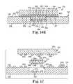
- FIG. 17is sectional view similar to FIG. 16B illustrating one further embodiment of the integrated circuit package in which both contact pads to be connected have a solder bump.
- FIGS. 18A-18Fillustrate an alternative method of assembling the integrated circuit package of FIG. 15 .
- FIGS. 1 and 2depict an integrated circuit package 10 in accordance with one preferred embodiment of the present invention.
- the integrated circuit package 10includes a package substrate 12 , a first integrated circuit (IC) die 14 , such as an IC memory die, and a second IC die 16 , such as a processor die.
- the package substrate 12includes an upper or first surface 18 and an opposite lower or second surface 20 .
- the first surface 18 of the package substrate 12defines a through opening 22 of the package substrate 12 .
- the through opening 22 of the package substrate 12is sized to accommodate the first IC die 14 .
- the length, width and depth dimensions of the recessed area 22are sized to fully accommodate the length, width and height dimensions of the first IC die 14 .
- the first surface 18 of the package substrate surrounding the through opening 22 of the package substrate 12includes a first land grid array of interconnection sites or first contact pads 26 .
- the first surface 18 of the package substrate 12also includes a second land grid array of interconnection sites or second contact pads 28 concentrically surrounding the first contact pads 26 .
- the dashed line 30 in FIG. 3depicts the dividing line between the first and second contacts pads 26 , 28 on the first surface 18 of the package substrate 12 .
- the first IC die 14includes a first surface 32 and an opposite second surface 34 .
- the second surface 34 of the first IC die 14includes a land grid array of interconnection sites or contact pads 38 .
- the second IC die 16includes a lower or first surface 42 and an opposite upper or second surface 44 .
- the first surface 42 of the second IC die 16includes a first land grid array of interconnection sites or first contact pads 46 .
- the first surface 42 of the second IC die 16further includes a second land grid array of interconnection sites or second contact pads 48 concentrically surrounded by the first contact pads 46 .
- Dashed lines 50 in FIG. 2depict the dividing line between the first and second contacts pads 46 , 48 on the first surface 42 of the second IC die 16 .
- the first contact pads 46 of the second IC die 16are electrically connected to the first contact pads 26 of the package substrate 12 by way of reflowed solder joints 52 .
- the second contact pads 48 of the second IC die 16are electrically connected to the contact pads 38 on the second surface 34 of the first IC die 14 by way of reflowed solder joints 54 .
- the first IC die 14is positioned amid (i.e., between) the package substrate 12 and the second IC die 16 .
- the first IC die 14is positioned within the through opening 22 of the package substrate 12 .
- the second contact pads 28 of the package substrate 12are provided for the electrical connection of further components (not shown).
- the second contact pads 28can take the form of traces that are connectable to other electronic components.
- the IC package 10could be in essence the main printed circuit board of an electronic component.
- the contact pads 26 , 28 , 38 , 46 , 48have been described as land grid arrays, the contact pads can take other forms, such as ball grid arrays.
- FIGS. 5A-5EAssembly of the integrated circuit package 10 (shown in FIGS. 1 and 2) in accordance with one preferred embodiment of the present invention is illustrated in FIGS. 5A-5E.
- FIG. 5Aillustrates the package substrate 12 , the first IC die 14 and the second IC die 16 of the integrated circuit package 10 at the start of the assembly process.
- solder bumps 58 and 60have been deposited in a known manner on the first and second contact pads 46 , 48 , respectively, on the first surface 42 of the second IC die 16 .
- FIG. 5Aillustrates the package substrate 12 , the first IC die 14 and the second IC die 16 of the integrated
- the first IC die 14has been positioned (i.e., engaged) with the second IC die 16 such that the contact pads 38 of the first IC die 14 are substantially aligned with the second contact pads 48 (i.e., solder bumps 60 ) of the second IC die 16 .
- the inherent tackiness of flux associated with the solder bumps 60tends to hold the first IC die 14 on the second IC die 16 .
- the second IC die 16is positioned (i.e., engaged) atop the package substrate 12 with the first IC die 14 positioned amid the package substrate 12 and the second IC die 16 .
- the first IC die 14is positioned within the through opening 22 of the package substrate 12 .
- the first contact pads 46i.e., solder bumps 58
- the second IC die 16are substantially aligned with the first contact pads 26 of the package substrate 12 .
- sufficient heatis applied to the IC package 10 (in a known manner) to simultaneously reflow the solder bumps 58 , 60 to simultaneously create the reflowed solder joints 52 , 54 thereby simultaneously electrically connecting together the package substrate 12 , the second IC die 16 and the first IC die 14 and completing assembly of the IC package 10 .
- epoxy 62may be used to just underfill gaps between the second IC die 16 and the package substrate 12 at the first contact pads 46 of the second IC die 16 and the first contact pads 26 of the package substrate 12 ; or epoxies 62 and 63 can be used to underfill gaps between the second IC die 16 and the package substrate 12 at the first contact pads 46 of the second IC die 16 and the first contact pads 26 of the package substrate 12 ; and gaps between the first IC die 14 and the second IC die 16 at the contact pads 38 of the first IC die 14 and the second contact pads 48 of the second IC die 16 .
- solder bumps 58 , 60are only deposited on the first and second contact pads 46 , 48 of the second IC die 16 , it is to be understood that alternatively the solder bumps could only be deposited on the first contact pads 26 of the package substrate 12 , and on the contact pads 38 of the first IC die 14 . As illustrated in FIG. 6, as a further alternative, solder bumps 64 can be applied to all of the contact pads 26 , 28 , 38 , 46 , 48 . Moreover, as even a further alternative to solder bumps and flux, a solder paste can be employed.
- FIGS. 7A-7FAssembly of the integrated circuit package 10 (shown in FIGS. 1 and 2) in accordance with one alternative embodiment of the present invention is illustrated in FIGS. 7A-7F.
- the steps depicted in FIGS. 7A and 7Bare identical to the steps previously described in connection with FIGS. 5A and 5B.
- FIG. 7Cthe first IC die 14 has been positioned (i.e., engaged) with the second IC die 16 such that the contact pads 38 of the first IC die 14 are substantially aligned with the second contact pads 48 (i.e., solder bumps 60 ) of the second IC die 16 .
- the second contact pads 48i.e., solder bumps 60
- the physical integrity of the IC package 10 assembled with this alternative methodcan, if desired, be optimized by underfilling one or all gaps in the IC package with a suitable epoxy as previously discussed with regards to FIG. 5 E.
- the particular contact pads that have solder bumps deposited thereoncan be varied as previously described above.
- FIGS. 8 and 9depict one alternative integrated circuit package 10 a .
- the integrated circuit package 10 aincludes the package substrate 12 a , the first integrated circuit (IC) die 14 a , and the second IC die 16 a .
- the first surface 18 a of the package substrate 12 adefines a recessed area 70 (instead of the through opening 22 ).
- the recessed area 70 of the package substrate 12 ais sized to accommodate: the first IC die 14 a . In particular, the length, width and depth dimensions of the.
- the recessed area 70are sized to fully accommodate the length, width and height dimensions of the first IC die 14 a .
- the first surface 18 a in the recessed area 70 of the package substrate 12 aincludes a further land grid array of interconnection sites or further contact pads 24 .
- the first contact pads 26 aconcentrically surround the recessed area 70 and the further contact pads 24 therein.
- the first surface 32 aincludes a land grid array of interconnection sites or additional contact pads 36 .
- the first IC die 14 ais positioned within the recessed area 70 of the package substrate 12 a , with the additional contact pads 36 of the first IC die 14 a electrically connected to the further contact pads 24 of the package substrate 12 a by way of reflowed solder joints 40 .
- the reflowed solder joints 52 aconnect the first contact pads 26 a of the package substrate 12 a to the first contact pads 46 a of the second IC die 16 a .
- the contact pads 38 and 48 and the reflowed solder joints 54 of the embodiment of FIGS. 1-7Fhave been eliminated and the first IC die 14 a is electrically connected to the second IC die 16 a through the package substrate 12 a.
- FIGS. 12A-12EAssembly of the one alternative embodiment integrated circuit package 10 a (shown in FIGS. 8 and 9) in accordance with one embodiment of the present invention is illustrated in FIGS. 12A-12E.
- FIG. 12Aillustrates the package substrate 12 a , the first IC die 14 a and the second IC die 16 a of the integrated circuit package 10 a at the start of the assembly process.
- solder bumps 56have been deposited on the additional contact pads 36 on the first surface 32 a of the first IC die 14 a
- the solder bumps 58 ahave been deposited on the contact pads 46 a on the first surface 42 a of the second IC die 16 a .
- FIG. 12Aillustrates the package substrate 12 a , the first IC die 14 a and the second IC die 16 a of the integrated circuit package 10 a at the start of the assembly process.
- solder bumps 56have been deposited on the additional contact pads 36 on the first surface 32 a of the first IC die 14
- the first IC die 14 ahas been positioned (i.e., engaged) in the recessed area 70 of the package substrate 12 a such that the first contact pads 36 (i.e., solder bumps 56 ) of the first IC die 14 are substantially aligned with the first contact pads 24 of the package substrate 12 a .
- the second IC die 16 ahas been positioned (i.e., engaged) atop the package substrate 12 a with the first IC die 14 a positioned between the package substrate 12 a and the second IC die 16 a and in the recessed area 70 .
- the first contact pads 46 ai.e., solder bumps 58 a
- the second IC die 16 aare substantially aligned with the first contact pads 26 a of the package substrate 12 a .
- sufficient heatis applied to the IC package 10 to simultaneously reflow the solder bumps 56 , 58 a to simultaneously create the reflowed solder joints 40 , 52 a thereby simultaneously electrically connecting together the package substrate 12 a , the first IC die 14 a and the second IC die 16 a and completing assembly of the IC package 10 .
- solder bumps 64 acan be applied to all of the contact pads 24 , 26 , 28 , 36 , 46 .
- FIGS. 14A-14FAssembly of the one alternative integrated circuit package 10 a (shown in FIGS. 8 and 9) in accordance with one alternative embodiment of the present invention is illustrated in FIGS. 14A-14F.
- the steps depicted in FIGS. 14A and 14Bare identical to the steps previously described in connection with FIGS. 12A and 12B.
- FIG. 14Cthe first IC die 14 a has been positioned (i.e., engaged) in the recessed area 70 of the package substrate 12 a such that the additional contact pads 36 (i.e., solder bumps 56 ) of the first IC die 14 a are substantially aligned with the further contact pads 24 of the package substrate 12 a .
- FIG. 14Cthe additional contact pads 36 (i.e., solder bumps 56 ) of the first IC die 14 a are substantially aligned with the further contact pads 24 of the package substrate 12 a .
- FIG. 14Ethe second IC die 16 a has been positioned (i.e., engaged) atop the package substrate 12 a with the first IC die 14 a positioned between the package substrate 12 a and the second IC die 16 a and in the recessed area 70 .
- the first contact pads 46 ai.e., solder bumps 58 a
- the second IC die 16 aare substantially aligned with the second contact pads 26 a of the package substrate 12 a .
- FIG. 15depicts one further embodiment integrated circuit package 10 b .
- the integrated circuit package 10 bis a combination of integrated circuit package 10 (FIGS. 1-7F) and integrated circuit package 10 a (FIGS. 8 - 14 F). As such like parts are labeled with like numerals except for the inclusion of “b”.
- the integrated circuit package 10 bincludes the package substrate 12 b , the first integrated circuit (IC) die 14 b , and the second IC die 16 b .
- the first surface 18 b of the package substrate 12 bincludes the recessed area 70 b sized to accommodate the first IC die 14 b.
- the first surface 18 b in the recessed area 70 bincludes the further contact pads 24 b .
- the first surface 18 b of the package substrate 12 balso includes the first contact pads 26 b and the second contact pads 28 b .
- the first surface 32 b of the first IC die 14 bincludes the additional contact pads 36 b
- the second surface 34 b of the first IC die 14 bincludes the contact pads 38 b .
- the first surface 42 b of the second IC die 16 bincludes the first and second contact pads 46 b , 48 b .
- the first IC die 14 bis positioned within the recessed area 70 b of the package substrate 12 b , with the additional contact pads 36 b of the first IC die 14 b electrically connected to the further contact pads 24 b of the package substrate 12 b by way of the reflowed solder joints 40 b .
- the first contact pads 46 bare electrically connected to the first contact pads 26 b of the package substrate 12 b by way of the reflowed solder joints 52 b .
- the second contact pads 48 bare electrically connected to the contact pads 38 b of the first IC die 14 b by way of reflowed solder joints 54 b.
- FIGS. 16A-16EAssembly of the integrated circuit package 10 b (shown in FIG. 15) in accordance with one embodiment is illustrated in FIGS. 16A-16E.
- FIG. 16Aillustrates the package substrate 12 b , the first IC die 14 b and the second IC die 16 b of the integrated circuit package 10 b at the start of the assembly process.
- solder bumps 56 bhave been deposited on the additional contact pads 36 b on the first surface 32 b of the first IC die 14 b
- solder bumps 58 b and 60 bhave been deposited on the first and second contact pads 46 b , 48 b , respectively, on the first surface 42 b of the second IC die 16 b .
- FIG. 16Aillustrates the package substrate 12 b , the first IC die 14 b and the second IC die 16 b of the integrated circuit package 10 b at the start of the assembly process.
- solder bumps 56 bhave been deposited on the additional contact pads 36 b on the
- the first IC die 14 bhas been positioned (i.e., engaged) in the recessed area 70 b of the package substrate 12 b such that the additional contact pads 36 b (i.e., solder bumps 56 b ) of the first IC die 14 b are substantially aligned with the further contact pads 24 b of the package substrate 12 b .
- the second IC die 16 bis positioned (i.e., engaged) atop the package substrate 12 b with the first IC die 14 b positioned between the package substrate 12 b and the second IC die 16 b and in the recessed area 70 b .
- the first contact pads 46 bi.e., solder bumps 58 b
- the second contact pads 48 bi.e., solder bumps 60 b
- the contact pads 38 b on the second surface 34 b of the first IC die 14 bare substantially aligned with the contact pads 38 b on the second surface 34 b of the first IC die 14 b .
- solder bumps 64 bcan be applied to all of the contact pads 24 b , 26 b , 28 b , 36 b , 38 b , 46 b , 48 b.
- FIGS. 18A-18FAssembly of the integrated circuit package 10 b (shown in FIG. 15) in accordance with one alternative embodiment of the present invention is illustrated in FIGS. 18A-18F.
- the steps of FIGS. 18A and 18Bare identical to FIGS. 16A and 16B.
- FIG. 18Cthe first IC die 14 b has been positioned (i.e., engaged) in the recessed area 70 b of the package substrate 12 b such that the additional contact pads 36 b (i.e., solder bumps 56 b ) are substantially aligned, with the further contact pads 24 b .
- the additional contact pads 36 bi.e., solder bumps 56 b
- the first contact pads 46 bi.e., solder bumps 58 b
- the second contact pads 48 bi.e., solder bumps 60 b
- the contact pads 38 b on the second surface 34 b of the first IC die 14 bare substantially aligned with the contact pads 38 b on the second surface 34 b of the first IC die 14 b .
- This integrated circuit package 10 , 10 a , 10 b assembled using flip-chip bonding techniqueshas low interconnect capacitance, thereby improving signal speed and substantially eliminating the need for off chip driver cells between the first and second IC dies. Moreover the assembly process of the integrated circuit package 10 , 10 a , 10 b is amenable to high volume low defect manufacturing.
Landscapes
- Engineering & Computer Science (AREA)
- Microelectronics & Electronic Packaging (AREA)
- Power Engineering (AREA)
- Physics & Mathematics (AREA)
- Condensed Matter Physics & Semiconductors (AREA)
- General Physics & Mathematics (AREA)
- Computer Hardware Design (AREA)
- Wire Bonding (AREA)
Abstract
Description
Claims (11)
Priority Applications (3)
| Application Number | Priority Date | Filing Date | Title |
|---|---|---|---|
| US10/199,441US6659512B1 (en) | 2002-07-18 | 2002-07-18 | Integrated circuit package employing flip-chip technology and method of assembly |
| US10/636,993US7002254B2 (en) | 2002-07-18 | 2003-08-06 | Integrated circuit package employing flip-chip technology and method of assembly |
| US10/677,078US20040036152A1 (en) | 2002-07-18 | 2003-09-30 | Integrated circuit package employing flip-chip technology and method of assembly |
Applications Claiming Priority (1)
| Application Number | Priority Date | Filing Date | Title |
|---|---|---|---|
| US10/199,441US6659512B1 (en) | 2002-07-18 | 2002-07-18 | Integrated circuit package employing flip-chip technology and method of assembly |
Related Child Applications (2)
| Application Number | Title | Priority Date | Filing Date |
|---|---|---|---|
| US10/636,993DivisionUS7002254B2 (en) | 2002-07-18 | 2003-08-06 | Integrated circuit package employing flip-chip technology and method of assembly |
| US10/677,078DivisionUS20040036152A1 (en) | 2002-07-18 | 2003-09-30 | Integrated circuit package employing flip-chip technology and method of assembly |
Publications (1)
| Publication Number | Publication Date |
|---|---|
| US6659512B1true US6659512B1 (en) | 2003-12-09 |
Family
ID=29711467
Family Applications (3)
| Application Number | Title | Priority Date | Filing Date |
|---|---|---|---|
| US10/199,441Expired - LifetimeUS6659512B1 (en) | 2002-07-18 | 2002-07-18 | Integrated circuit package employing flip-chip technology and method of assembly |
| US10/636,993Expired - Fee RelatedUS7002254B2 (en) | 2002-07-18 | 2003-08-06 | Integrated circuit package employing flip-chip technology and method of assembly |
| US10/677,078AbandonedUS20040036152A1 (en) | 2002-07-18 | 2003-09-30 | Integrated circuit package employing flip-chip technology and method of assembly |
Family Applications After (2)
| Application Number | Title | Priority Date | Filing Date |
|---|---|---|---|
| US10/636,993Expired - Fee RelatedUS7002254B2 (en) | 2002-07-18 | 2003-08-06 | Integrated circuit package employing flip-chip technology and method of assembly |
| US10/677,078AbandonedUS20040036152A1 (en) | 2002-07-18 | 2003-09-30 | Integrated circuit package employing flip-chip technology and method of assembly |
Country Status (1)
| Country | Link |
|---|---|
| US (3) | US6659512B1 (en) |
Cited By (72)
| Publication number | Priority date | Publication date | Assignee | Title |
|---|---|---|---|---|
| US20040012094A1 (en)* | 2002-07-18 | 2004-01-22 | Harper Timothy V. | Flip-chip integrated circuit package and method of assembly |
| US20040067605A1 (en)* | 2002-10-02 | 2004-04-08 | Shinko Electric Industries, Co., Ltd. | Semiconductor device having additional functional element and method of manufacturing thereof |
| US20040130017A1 (en)* | 2002-12-20 | 2004-07-08 | Renesas Technology Corp. | Stacked layer type semiconductor device and its manufacturing method |
| US20040195699A1 (en)* | 2003-04-04 | 2004-10-07 | Massingill Thomas Joel | Semiconductor package with recess for die |
| US20040212067A1 (en)* | 2003-04-25 | 2004-10-28 | Advanced Semiconductor Engineering, Inc. | Multi-chips stacked package |
| US20040225761A1 (en)* | 2003-03-13 | 2004-11-11 | Carsten Mitter | Communication device having asynchronous data tranmission via symmetrical serial interface |
| US20040262774A1 (en)* | 2003-06-27 | 2004-12-30 | In-Ku Kang | Multi-chip packages having a plurality of flip chips and methods of manufacturing the same |
| US20050285254A1 (en)* | 2004-06-23 | 2005-12-29 | Buot Joan R V | Semiconducting device having stacked dice |
| US20060220239A1 (en)* | 2005-03-11 | 2006-10-05 | Tyco Electronics Corporation | LGA socket with emi protection |
| US20060283627A1 (en)* | 2005-06-17 | 2006-12-21 | Advanced Seminconductor Engineering, Inc. | Substrate structure of integrated embedded passive components and method for fabricating the same |
| US20070008704A1 (en)* | 1998-08-18 | 2007-01-11 | Oki Electric Industry Co., Ltd. | Package structure for a semiconductor device |
| US20070069371A1 (en)* | 2005-09-29 | 2007-03-29 | United Test And Assembly Center Ltd. | Cavity chip package |
| US20090321959A1 (en)* | 2008-06-27 | 2009-12-31 | Harry Hedler | Chip Arrangement and Method of Manufacturing a Chip Arrangement |
| US20100020585A1 (en)* | 2005-09-02 | 2010-01-28 | Rajan Suresh N | Methods and apparatus of stacking drams |
| US20100065948A1 (en)* | 2008-09-12 | 2010-03-18 | Stats Chippac, Ltd. | Semiconductor Device and Method of Forming a Fan-In Package-on-Package Structure Using Through-Silicon Vias |
| US20100281280A1 (en)* | 2006-07-31 | 2010-11-04 | Google Inc. | Interface Circuit System And Method For Performing Power Management Operations In Conjunction With Only A Portion Of A Memory Circuit |
| US20110068459A1 (en)* | 2009-09-23 | 2011-03-24 | Stats Chippac, Ltd. | Semiconductor Device and Method of Forming Interposer with Opening to Contain Semiconductor Die |
| US20110215451A1 (en)* | 2010-03-02 | 2011-09-08 | Samsung Electronics Co., Ltd. | Stacked Semiconductor Packages |
| US8041881B2 (en) | 2006-07-31 | 2011-10-18 | Google Inc. | Memory device with emulated characteristics |
| US8055833B2 (en) | 2006-10-05 | 2011-11-08 | Google Inc. | System and method for increasing capacity, performance, and flexibility of flash storage |
| US8060774B2 (en) | 2005-06-24 | 2011-11-15 | Google Inc. | Memory systems and memory modules |
| US8080874B1 (en)* | 2007-09-14 | 2011-12-20 | Google Inc. | Providing additional space between an integrated circuit and a circuit board for positioning a component therebetween |
| US8089795B2 (en) | 2006-02-09 | 2012-01-03 | Google Inc. | Memory module with memory stack and interface with enhanced capabilities |
| US8090897B2 (en) | 2006-07-31 | 2012-01-03 | Google Inc. | System and method for simulating an aspect of a memory circuit |
| US8111566B1 (en) | 2007-11-16 | 2012-02-07 | Google, Inc. | Optimal channel design for memory devices for providing a high-speed memory interface |
| US8122207B2 (en) | 2006-07-31 | 2012-02-21 | Google Inc. | Apparatus and method for power management of memory circuits by a system or component thereof |
| US8130560B1 (en) | 2006-11-13 | 2012-03-06 | Google Inc. | Multi-rank partial width memory modules |
| US8154935B2 (en) | 2006-07-31 | 2012-04-10 | Google Inc. | Delaying a signal communicated from a system to at least one of a plurality of memory circuits |
| US8169233B2 (en) | 2009-06-09 | 2012-05-01 | Google Inc. | Programming of DIMM termination resistance values |
| US20120147571A1 (en)* | 2010-12-14 | 2012-06-14 | Just Andrew B | Printed circuit board radio-frequency shielding structures |
| US8244971B2 (en) | 2006-07-31 | 2012-08-14 | Google Inc. | Memory circuit system and method |
| US8280714B2 (en) | 2006-07-31 | 2012-10-02 | Google Inc. | Memory circuit simulation system and method with refresh capabilities |
| US8327104B2 (en) | 2006-07-31 | 2012-12-04 | Google Inc. | Adjusting the timing of signals associated with a memory system |
| US8335894B1 (en) | 2008-07-25 | 2012-12-18 | Google Inc. | Configurable memory system with interface circuit |
| US20130017724A1 (en)* | 2011-07-13 | 2013-01-17 | Gang Liu | Emi-preventing socket and manufacturing method thereof |
| US8386722B1 (en) | 2008-06-23 | 2013-02-26 | Google Inc. | Stacked DIMM memory interface |
| US8438328B2 (en) | 2008-02-21 | 2013-05-07 | Google Inc. | Emulation of abstracted DIMMs using abstracted DRAMs |
| US8566516B2 (en) | 2006-07-31 | 2013-10-22 | Google Inc. | Refresh management of memory modules |
| RU2498452C2 (en)* | 2009-06-24 | 2013-11-10 | Интел Корпорейшн | Polychip-dip and method for presentation of crystals interconnection in it |
| US8598695B2 (en) | 2010-07-23 | 2013-12-03 | Tessera, Inc. | Active chip on carrier or laminated chip having microelectronic element embedded therein |
| US8654537B2 (en) | 2010-12-01 | 2014-02-18 | Apple Inc. | Printed circuit board with integral radio-frequency shields |
| US20140070380A1 (en)* | 2012-09-11 | 2014-03-13 | Chia-Pin Chiu | Bridge interconnect with air gap in package assembly |
| US8705240B1 (en) | 2007-12-18 | 2014-04-22 | Google Inc. | Embossed heat spreader |
| US8773937B2 (en) | 2005-06-24 | 2014-07-08 | Google Inc. | Memory refresh apparatus and method |
| US8796830B1 (en) | 2006-09-01 | 2014-08-05 | Google Inc. | Stackable low-profile lead frame package |
| US20140246773A1 (en)* | 2013-03-04 | 2014-09-04 | Dialog Semiconductor Gmbh | Chip on Chip Attach (Passive IPD and PMIC) Flip Chip BGA Using New Cavity BGA Substrate |
| US8949519B2 (en) | 2005-06-24 | 2015-02-03 | Google Inc. | Simulating a memory circuit |
| US8977806B1 (en) | 2006-10-05 | 2015-03-10 | Google Inc. | Hybrid memory module |
| US9048306B2 (en) | 2009-09-23 | 2015-06-02 | Stats Chippac, Ltd. | Semiconductor device and method of forming open cavity in TSV interposer to contain semiconductor die in WLCSMP |
| US20150249065A1 (en)* | 2010-09-07 | 2015-09-03 | Stats Chippac, Ltd. | Semiconductor Device and Method of Forming WLP With Semiconductor Die Embedded Within Penetrable Encapsulant Between TSV Interposers |
| US9171585B2 (en) | 2005-06-24 | 2015-10-27 | Google Inc. | Configurable memory circuit system and method |
| US9179538B2 (en) | 2011-06-09 | 2015-11-03 | Apple Inc. | Electromagnetic shielding structures for selectively shielding components on a substrate |
| US20160240457A1 (en)* | 2015-02-18 | 2016-08-18 | Altera Corporation | Integrated circuit packages with dual-sided stacking structure |
| US9507739B2 (en) | 2005-06-24 | 2016-11-29 | Google Inc. | Configurable memory circuit system and method |
| US9515052B1 (en)* | 2015-06-26 | 2016-12-06 | SK Hynix Inc. | Semiconductor package including a step type substrate |
| US9542352B2 (en) | 2006-02-09 | 2017-01-10 | Google Inc. | System and method for reducing command scheduling constraints of memory circuits |
| US9576942B1 (en)* | 2015-12-18 | 2017-02-21 | Intel Corporation | Integrated circuit assembly that includes stacked dice |
| US9632929B2 (en) | 2006-02-09 | 2017-04-25 | Google Inc. | Translating an address associated with a command communicated between a system and memory circuits |
| US20170287879A1 (en)* | 2014-03-28 | 2017-10-05 | SK Hynix Inc. | Thin stack packages |
| US9806061B2 (en)* | 2016-03-31 | 2017-10-31 | Altera Corporation | Bumpless wafer level fan-out package |
| JP2018093007A (en)* | 2016-12-01 | 2018-06-14 | 富士通株式会社 | Optical module and manufacturing method thereof |
| US10013371B2 (en) | 2005-06-24 | 2018-07-03 | Google Llc | Configurable memory circuit system and method |
| US20180286833A1 (en)* | 2017-03-29 | 2018-10-04 | Intel Corporation | Microelectronics Package Providing Increased Memory Component Density |
| US10121768B2 (en) | 2015-05-27 | 2018-11-06 | Bridge Semiconductor Corporation | Thermally enhanced face-to-face semiconductor assembly with built-in heat spreader and method of making the same |
| US10163772B2 (en)* | 2015-09-17 | 2018-12-25 | Semiconductor Components Industries, Llc | Stacked semiconductor device structure and method |
| CN110024108A (en)* | 2016-12-31 | 2019-07-16 | 英特尔公司 | Electronic package assembly with stiffener |
| US10354984B2 (en) | 2015-05-27 | 2019-07-16 | Bridge Semiconductor Corporation | Semiconductor assembly with electromagnetic shielding and thermally enhanced characteristics and method of making the same |
| US10438894B1 (en)* | 2018-05-30 | 2019-10-08 | Globalfoundries Inc. | Chip-to-chip and chip-to-substrate interconnections in multi-chip semiconductor devices |
| US20200373289A1 (en)* | 2016-12-07 | 2020-11-26 | STATS ChipPAC Pte. Ltd. | Semiconductor Device and Method of Forming a 3D Interposer System-in-Package Module |
| US20210375845A1 (en)* | 2020-05-27 | 2021-12-02 | Qualcomm Incorporated | Package cavity for enhanced device performance with an integrated passive device |
| US11291146B2 (en) | 2014-03-07 | 2022-03-29 | Bridge Semiconductor Corp. | Leadframe substrate having modulator and crack inhibiting structure and flip chip assembly using the same |
| CN116953862A (en)* | 2022-04-19 | 2023-10-27 | 武汉光迅科技股份有限公司 | A 3D packaged optical transceiver component and its use method |
Families Citing this family (42)
| Publication number | Priority date | Publication date | Assignee | Title |
|---|---|---|---|---|
| TWI313507B (en)* | 2002-10-25 | 2009-08-11 | Megica Corporatio | Method for assembling chips |
| JP4198566B2 (en)* | 2003-09-29 | 2008-12-17 | 新光電気工業株式会社 | Manufacturing method of electronic component built-in substrate |
| US8129841B2 (en) | 2006-12-14 | 2012-03-06 | Stats Chippac, Ltd. | Solder joint flip chip interconnection |
| TWI378516B (en) | 2003-11-10 | 2012-12-01 | Chippac Inc | Bump-on-lead flip chip interconnection |
| US9029196B2 (en) | 2003-11-10 | 2015-05-12 | Stats Chippac, Ltd. | Semiconductor device and method of self-confinement of conductive bump material during reflow without solder mask |
| USRE47600E1 (en) | 2003-11-10 | 2019-09-10 | STATS ChipPAC Pte. Ltd. | Semiconductor device and method of forming electrical interconnect with stress relief void |
| US8574959B2 (en) | 2003-11-10 | 2013-11-05 | Stats Chippac, Ltd. | Semiconductor device and method of forming bump-on-lead interconnection |
| US8216930B2 (en) | 2006-12-14 | 2012-07-10 | Stats Chippac, Ltd. | Solder joint flip chip interconnection having relief structure |
| US8026128B2 (en) | 2004-11-10 | 2011-09-27 | Stats Chippac, Ltd. | Semiconductor device and method of self-confinement of conductive bump material during reflow without solder mask |
| GB2416917A (en)* | 2004-07-30 | 2006-02-08 | Univ Kent Canterbury | Multiple chip semiconductor device |
| JP4808729B2 (en)* | 2004-11-12 | 2011-11-02 | アナログ デバイシーズ インク | Spacing butted component structure |
| KR20070107154A (en) | 2005-03-25 | 2007-11-06 | 스태츠 칩팩, 엘티디. | Flip chip interconnects with narrow interconnect sites on the substrate |
| US8841779B2 (en) | 2005-03-25 | 2014-09-23 | Stats Chippac, Ltd. | Semiconductor device and method of forming high routing density BOL BONL and BONP interconnect sites on substrate |
| US8476591B2 (en) | 2005-09-21 | 2013-07-02 | Analog Devices, Inc. | Radiation sensor device and method |
| JP5013973B2 (en)* | 2007-05-31 | 2012-08-29 | 株式会社メイコー | Printed wiring board and method for manufacturing the same, electronic component housing board using the printed wiring board, and method for manufacturing the same |
| US8247267B2 (en) | 2008-03-11 | 2012-08-21 | Taiwan Semiconductor Manufacturing Company, Ltd. | Wafer level IC assembly method |
| US8836115B1 (en)* | 2008-07-31 | 2014-09-16 | Amkor Technology, Inc. | Stacked inverted flip chip package and fabrication method |
| US8390083B2 (en) | 2009-09-04 | 2013-03-05 | Analog Devices, Inc. | System with recessed sensing or processing elements |
| WO2012051340A1 (en) | 2010-10-12 | 2012-04-19 | Analog Devices, Inc. | Microphone package with embedded asic |
| US9799627B2 (en)* | 2012-01-19 | 2017-10-24 | Semiconductor Components Industries, Llc | Semiconductor package structure and method |
| US8866308B2 (en) | 2012-12-20 | 2014-10-21 | Intel Corporation | High density interconnect device and method |
| US9847462B2 (en) | 2013-10-29 | 2017-12-19 | Point Engineering Co., Ltd. | Array substrate for mounting chip and method for manufacturing the same |
| US10217790B2 (en)* | 2015-01-15 | 2019-02-26 | Koninklijke Philips N.V. | Imaging detector module assembly |
| US9666558B2 (en) | 2015-06-29 | 2017-05-30 | Point Engineering Co., Ltd. | Substrate for mounting a chip and chip package using the substrate |
| US10665579B2 (en)* | 2016-02-16 | 2020-05-26 | Xilinx, Inc. | Chip package assembly with power management integrated circuit and integrated circuit die |
| CN108091629B (en)* | 2017-12-08 | 2020-01-10 | 华进半导体封装先导技术研发中心有限公司 | Photoelectric chip integrated structure |
| US11348897B2 (en) | 2017-12-29 | 2022-05-31 | Intel Corporation | Microelectronic assemblies |
| WO2019132970A1 (en) | 2017-12-29 | 2019-07-04 | Intel Corporation | Microelectronic assemblies |
| US11342320B2 (en) | 2017-12-29 | 2022-05-24 | Intel Corporation | Microelectronic assemblies |
| WO2019132967A1 (en) | 2017-12-29 | 2019-07-04 | Intel Corporation | Microelectronic assemblies |
| US11494682B2 (en) | 2017-12-29 | 2022-11-08 | Intel Corporation | Quantum computing assemblies |
| US11469206B2 (en) | 2018-06-14 | 2022-10-11 | Intel Corporation | Microelectronic assemblies |
| US11581287B2 (en)* | 2018-06-29 | 2023-02-14 | Intel Corporation | Chip scale thin 3D die stacked package |
| US11145624B2 (en) | 2019-07-26 | 2021-10-12 | Advanced Semiconductor Engineering, Inc. | Semiconductor device package and method for manufacturing the same |
| US12272650B2 (en) | 2020-02-28 | 2025-04-08 | Intel Corporation | Microelectronic package with substrate cavity for bridge-attach |
| CN113766731A (en)* | 2020-06-02 | 2021-12-07 | 苏州旭创科技有限公司 | Assembling method of circuit board assembly |
| US11373972B2 (en) | 2020-06-16 | 2022-06-28 | Intel Corporation | Microelectronic structures including bridges |
| US11923307B2 (en) | 2020-06-16 | 2024-03-05 | Intel Corporation | Microelectronic structures including bridges |
| US11887962B2 (en) | 2020-06-16 | 2024-01-30 | Intel Corporation | Microelectronic structures including bridges |
| US11791274B2 (en) | 2020-06-16 | 2023-10-17 | Intel Corporation | Multichip semiconductor package including a bridge die disposed in a cavity having non-planar interconnects |
| US11804441B2 (en)* | 2020-06-16 | 2023-10-31 | Intel Corporation | Microelectronic structures including bridges |
| US12412868B2 (en) | 2021-12-21 | 2025-09-09 | Intel Corporation | Microelectronic assemblies including interconnects with different solder materials |
Citations (25)
| Publication number | Priority date | Publication date | Assignee | Title |
|---|---|---|---|---|
| US5564617A (en) | 1992-09-03 | 1996-10-15 | Lucent Technologies Inc. | Method and apparatus for assembling multichip modules |
| US5671530A (en) | 1995-10-30 | 1997-09-30 | Delco Electronics Corporation | Flip-chip mounting assembly and method with vertical wafer feeder |
| US5723369A (en) | 1996-03-14 | 1998-03-03 | Lsi Logic Corporation | Method of flip chip assembly |
| US5760478A (en)* | 1996-08-20 | 1998-06-02 | International Business Machines Corporation | Clock skew minimization system and method for integrated circuits |
| US5790384A (en)* | 1997-06-26 | 1998-08-04 | International Business Machines Corporation | Bare die multiple dies for direct attach |
| US5798567A (en)* | 1997-08-21 | 1998-08-25 | Hewlett-Packard Company | Ball grid array integrated circuit package which employs a flip chip integrated circuit and decoupling capacitors |
| US5801072A (en) | 1996-03-14 | 1998-09-01 | Lsi Logic Corporation | Method of packaging integrated circuits |
| US5804882A (en)* | 1995-05-22 | 1998-09-08 | Hitachi Chemical Company, Ltd. | Semiconductor device having a semiconductor chip electrically connected to a wiring substrate |
| US6084308A (en)* | 1998-06-30 | 2000-07-04 | National Semiconductor Corporation | Chip-on-chip integrated circuit package and method for making the same |
| US6098278A (en) | 1994-06-23 | 2000-08-08 | Cubic Memory, Inc. | Method for forming conductive epoxy flip-chip on chip |
| US6150724A (en)* | 1998-03-02 | 2000-11-21 | Motorola, Inc. | Multi-chip semiconductor device and method for making the device by using multiple flip chip interfaces |
| US6189208B1 (en) | 1998-09-11 | 2001-02-20 | Polymer Flip Chip Corp. | Flip chip mounting technique |
| US6190940B1 (en) | 1999-01-21 | 2001-02-20 | Lucent Technologies Inc. | Flip chip assembly of semiconductor IC chips |
| US6201301B1 (en) | 1998-01-21 | 2001-03-13 | Lsi Logic Corporation | Low cost thermally enhanced flip chip BGA |
| US6225699B1 (en)* | 1998-06-26 | 2001-05-01 | International Business Machines Corporation | Chip-on-chip interconnections of varied characteristics |
| US6271598B1 (en) | 1997-07-29 | 2001-08-07 | Cubic Memory, Inc. | Conductive epoxy flip-chip on chip |
| US6291267B1 (en)* | 1999-06-09 | 2001-09-18 | International Business Machines Corporation | Process for underfilling chip-under-chip semiconductor modules |
| US6292368B1 (en)* | 1999-03-09 | 2001-09-18 | Sagem Sa | Electrical power component mounted by brazing on a support and corresponding mounting process |
| US6294406B1 (en)* | 1998-06-26 | 2001-09-25 | International Business Machines Corporation | Highly integrated chip-on-chip packaging |
| US6365963B1 (en)* | 1999-09-02 | 2002-04-02 | Nec Corporation | Stacked-chip semiconductor device |
| US6369448B1 (en)* | 2000-01-21 | 2002-04-09 | Lsi Logic Corporation | Vertically integrated flip chip semiconductor package |
| US6489686B2 (en)* | 1999-12-21 | 2002-12-03 | International Business Machines Corporation | Multi-cavity substrate structure for discrete devices |
| US6489669B2 (en)* | 2000-09-11 | 2002-12-03 | Rohm Co., Ltd. | Integrated circuit device |
| US6492726B1 (en)* | 2000-09-22 | 2002-12-10 | Chartered Semiconductor Manufacturing Ltd. | Chip scale packaging with multi-layer flip chip arrangement and ball grid array interconnection |
| US6521984B2 (en)* | 2000-11-07 | 2003-02-18 | Mitsubishi Denki Kabushiki Kaisha | Semiconductor module with semiconductor devices attached to upper and lower surface of a semiconductor substrate |
Family Cites Families (3)
| Publication number | Priority date | Publication date | Assignee | Title |
|---|---|---|---|---|
| JPS6080232A (en)* | 1983-10-11 | 1985-05-08 | Nippon Telegr & Teleph Corp <Ntt> | Lsi chip mounting card |
| EP0637509B1 (en)* | 1993-08-03 | 2002-10-23 | Nitta Moore Company | A tube for fuel transportation |
| US5567654A (en)* | 1994-09-28 | 1996-10-22 | International Business Machines Corporation | Method and workpiece for connecting a thin layer to a monolithic electronic module's surface and associated module packaging |
- 2002
- 2002-07-18USUS10/199,441patent/US6659512B1/ennot_activeExpired - Lifetime
- 2003
- 2003-08-06USUS10/636,993patent/US7002254B2/ennot_activeExpired - Fee Related
- 2003-09-30USUS10/677,078patent/US20040036152A1/ennot_activeAbandoned
Patent Citations (25)
| Publication number | Priority date | Publication date | Assignee | Title |
|---|---|---|---|---|
| US5564617A (en) | 1992-09-03 | 1996-10-15 | Lucent Technologies Inc. | Method and apparatus for assembling multichip modules |
| US6098278A (en) | 1994-06-23 | 2000-08-08 | Cubic Memory, Inc. | Method for forming conductive epoxy flip-chip on chip |
| US5804882A (en)* | 1995-05-22 | 1998-09-08 | Hitachi Chemical Company, Ltd. | Semiconductor device having a semiconductor chip electrically connected to a wiring substrate |
| US5671530A (en) | 1995-10-30 | 1997-09-30 | Delco Electronics Corporation | Flip-chip mounting assembly and method with vertical wafer feeder |
| US5723369A (en) | 1996-03-14 | 1998-03-03 | Lsi Logic Corporation | Method of flip chip assembly |
| US5801072A (en) | 1996-03-14 | 1998-09-01 | Lsi Logic Corporation | Method of packaging integrated circuits |
| US5760478A (en)* | 1996-08-20 | 1998-06-02 | International Business Machines Corporation | Clock skew minimization system and method for integrated circuits |
| US5790384A (en)* | 1997-06-26 | 1998-08-04 | International Business Machines Corporation | Bare die multiple dies for direct attach |
| US6271598B1 (en) | 1997-07-29 | 2001-08-07 | Cubic Memory, Inc. | Conductive epoxy flip-chip on chip |
| US5798567A (en)* | 1997-08-21 | 1998-08-25 | Hewlett-Packard Company | Ball grid array integrated circuit package which employs a flip chip integrated circuit and decoupling capacitors |
| US6201301B1 (en) | 1998-01-21 | 2001-03-13 | Lsi Logic Corporation | Low cost thermally enhanced flip chip BGA |
| US6150724A (en)* | 1998-03-02 | 2000-11-21 | Motorola, Inc. | Multi-chip semiconductor device and method for making the device by using multiple flip chip interfaces |
| US6294406B1 (en)* | 1998-06-26 | 2001-09-25 | International Business Machines Corporation | Highly integrated chip-on-chip packaging |
| US6225699B1 (en)* | 1998-06-26 | 2001-05-01 | International Business Machines Corporation | Chip-on-chip interconnections of varied characteristics |
| US6084308A (en)* | 1998-06-30 | 2000-07-04 | National Semiconductor Corporation | Chip-on-chip integrated circuit package and method for making the same |
| US6189208B1 (en) | 1998-09-11 | 2001-02-20 | Polymer Flip Chip Corp. | Flip chip mounting technique |
| US6190940B1 (en) | 1999-01-21 | 2001-02-20 | Lucent Technologies Inc. | Flip chip assembly of semiconductor IC chips |
| US6292368B1 (en)* | 1999-03-09 | 2001-09-18 | Sagem Sa | Electrical power component mounted by brazing on a support and corresponding mounting process |
| US6291267B1 (en)* | 1999-06-09 | 2001-09-18 | International Business Machines Corporation | Process for underfilling chip-under-chip semiconductor modules |
| US6365963B1 (en)* | 1999-09-02 | 2002-04-02 | Nec Corporation | Stacked-chip semiconductor device |
| US6489686B2 (en)* | 1999-12-21 | 2002-12-03 | International Business Machines Corporation | Multi-cavity substrate structure for discrete devices |
| US6369448B1 (en)* | 2000-01-21 | 2002-04-09 | Lsi Logic Corporation | Vertically integrated flip chip semiconductor package |
| US6489669B2 (en)* | 2000-09-11 | 2002-12-03 | Rohm Co., Ltd. | Integrated circuit device |
| US6492726B1 (en)* | 2000-09-22 | 2002-12-10 | Chartered Semiconductor Manufacturing Ltd. | Chip scale packaging with multi-layer flip chip arrangement and ball grid array interconnection |
| US6521984B2 (en)* | 2000-11-07 | 2003-02-18 | Mitsubishi Denki Kabushiki Kaisha | Semiconductor module with semiconductor devices attached to upper and lower surface of a semiconductor substrate |
Cited By (141)
| Publication number | Priority date | Publication date | Assignee | Title |
|---|---|---|---|---|
| US20070008704A1 (en)* | 1998-08-18 | 2007-01-11 | Oki Electric Industry Co., Ltd. | Package structure for a semiconductor device |
| US7514768B2 (en)* | 1998-08-18 | 2009-04-07 | Oki Electric Industry Co., Ltd. | Package structure for a semiconductor device incorporating enhanced solder bump structure |
| US20040012094A1 (en)* | 2002-07-18 | 2004-01-22 | Harper Timothy V. | Flip-chip integrated circuit package and method of assembly |
| US20040067605A1 (en)* | 2002-10-02 | 2004-04-08 | Shinko Electric Industries, Co., Ltd. | Semiconductor device having additional functional element and method of manufacturing thereof |
| US7005747B2 (en)* | 2002-10-02 | 2006-02-28 | Shinko Electric Industries Co., Ltd. | Semiconductor device having additional functional element and method of manufacturing thereof |
| US20040130017A1 (en)* | 2002-12-20 | 2004-07-08 | Renesas Technology Corp. | Stacked layer type semiconductor device and its manufacturing method |
| US20040225761A1 (en)* | 2003-03-13 | 2004-11-11 | Carsten Mitter | Communication device having asynchronous data tranmission via symmetrical serial interface |
| US7188207B2 (en)* | 2003-03-13 | 2007-03-06 | Robert Bosch Gmbh | Communication device having asynchronous data transmission via symmetrical serial interface |
| US20040195699A1 (en)* | 2003-04-04 | 2004-10-07 | Massingill Thomas Joel | Semiconductor package with recess for die |
| US7239024B2 (en)* | 2003-04-04 | 2007-07-03 | Thomas Joel Massingill | Semiconductor package with recess for die |
| US20040212067A1 (en)* | 2003-04-25 | 2004-10-28 | Advanced Semiconductor Engineering, Inc. | Multi-chips stacked package |
| US20040262774A1 (en)* | 2003-06-27 | 2004-12-30 | In-Ku Kang | Multi-chip packages having a plurality of flip chips and methods of manufacturing the same |
| US20050285254A1 (en)* | 2004-06-23 | 2005-12-29 | Buot Joan R V | Semiconducting device having stacked dice |
| US7170169B2 (en)* | 2005-03-11 | 2007-01-30 | Tyco Electronics Corporation | LGA socket with EMI protection |
| US20060220239A1 (en)* | 2005-03-11 | 2006-10-05 | Tyco Electronics Corporation | LGA socket with emi protection |
| US20060283627A1 (en)* | 2005-06-17 | 2006-12-21 | Advanced Seminconductor Engineering, Inc. | Substrate structure of integrated embedded passive components and method for fabricating the same |
| US10013371B2 (en) | 2005-06-24 | 2018-07-03 | Google Llc | Configurable memory circuit system and method |
| US9171585B2 (en) | 2005-06-24 | 2015-10-27 | Google Inc. | Configurable memory circuit system and method |
| US8386833B2 (en) | 2005-06-24 | 2013-02-26 | Google Inc. | Memory systems and memory modules |
| US8359187B2 (en) | 2005-06-24 | 2013-01-22 | Google Inc. | Simulating a different number of memory circuit devices |
| US8949519B2 (en) | 2005-06-24 | 2015-02-03 | Google Inc. | Simulating a memory circuit |
| US8615679B2 (en) | 2005-06-24 | 2013-12-24 | Google Inc. | Memory modules with reliability and serviceability functions |
| US8060774B2 (en) | 2005-06-24 | 2011-11-15 | Google Inc. | Memory systems and memory modules |
| US8773937B2 (en) | 2005-06-24 | 2014-07-08 | Google Inc. | Memory refresh apparatus and method |
| US9507739B2 (en) | 2005-06-24 | 2016-11-29 | Google Inc. | Configurable memory circuit system and method |
| US8811065B2 (en) | 2005-09-02 | 2014-08-19 | Google Inc. | Performing error detection on DRAMs |
| US8619452B2 (en) | 2005-09-02 | 2013-12-31 | Google Inc. | Methods and apparatus of stacking DRAMs |
| US20100020585A1 (en)* | 2005-09-02 | 2010-01-28 | Rajan Suresh N | Methods and apparatus of stacking drams |
| US8213205B2 (en) | 2005-09-02 | 2012-07-03 | Google Inc. | Memory system including multiple memory stacks |
| US8582339B2 (en) | 2005-09-02 | 2013-11-12 | Google Inc. | System including memory stacks |
| US7339278B2 (en)* | 2005-09-29 | 2008-03-04 | United Test And Assembly Center Ltd. | Cavity chip package |
| US20070069371A1 (en)* | 2005-09-29 | 2007-03-29 | United Test And Assembly Center Ltd. | Cavity chip package |
| US9632929B2 (en) | 2006-02-09 | 2017-04-25 | Google Inc. | Translating an address associated with a command communicated between a system and memory circuits |
| US8566556B2 (en) | 2006-02-09 | 2013-10-22 | Google Inc. | Memory module with memory stack and interface with enhanced capabilities |
| US8797779B2 (en) | 2006-02-09 | 2014-08-05 | Google Inc. | Memory module with memory stack and interface with enhanced capabilites |
| US8089795B2 (en) | 2006-02-09 | 2012-01-03 | Google Inc. | Memory module with memory stack and interface with enhanced capabilities |
| US9542352B2 (en) | 2006-02-09 | 2017-01-10 | Google Inc. | System and method for reducing command scheduling constraints of memory circuits |
| US9727458B2 (en) | 2006-02-09 | 2017-08-08 | Google Inc. | Translating an address associated with a command communicated between a system and memory circuits |
| US8154935B2 (en) | 2006-07-31 | 2012-04-10 | Google Inc. | Delaying a signal communicated from a system to at least one of a plurality of memory circuits |
| US8112266B2 (en) | 2006-07-31 | 2012-02-07 | Google Inc. | Apparatus for simulating an aspect of a memory circuit |
| US8244971B2 (en) | 2006-07-31 | 2012-08-14 | Google Inc. | Memory circuit system and method |
| US8280714B2 (en) | 2006-07-31 | 2012-10-02 | Google Inc. | Memory circuit simulation system and method with refresh capabilities |
| US20100281280A1 (en)* | 2006-07-31 | 2010-11-04 | Google Inc. | Interface Circuit System And Method For Performing Power Management Operations In Conjunction With Only A Portion Of A Memory Circuit |
| US8327104B2 (en) | 2006-07-31 | 2012-12-04 | Google Inc. | Adjusting the timing of signals associated with a memory system |
| US8972673B2 (en) | 2006-07-31 | 2015-03-03 | Google Inc. | Power management of memory circuits by virtual memory simulation |
| US8340953B2 (en) | 2006-07-31 | 2012-12-25 | Google, Inc. | Memory circuit simulation with power saving capabilities |
| US8181048B2 (en) | 2006-07-31 | 2012-05-15 | Google Inc. | Performing power management operations |
| US8745321B2 (en) | 2006-07-31 | 2014-06-03 | Google Inc. | Simulating a memory standard |
| US8671244B2 (en) | 2006-07-31 | 2014-03-11 | Google Inc. | Simulating a memory standard |
| US8667312B2 (en) | 2006-07-31 | 2014-03-04 | Google Inc. | Performing power management operations |
| US8868829B2 (en) | 2006-07-31 | 2014-10-21 | Google Inc. | Memory circuit system and method |
| US8407412B2 (en) | 2006-07-31 | 2013-03-26 | Google Inc. | Power management of memory circuits by virtual memory simulation |
| US8122207B2 (en) | 2006-07-31 | 2012-02-21 | Google Inc. | Apparatus and method for power management of memory circuits by a system or component thereof |
| US8631220B2 (en) | 2006-07-31 | 2014-01-14 | Google Inc. | Adjusting the timing of signals associated with a memory system |
| US8566516B2 (en) | 2006-07-31 | 2013-10-22 | Google Inc. | Refresh management of memory modules |
| US9047976B2 (en) | 2006-07-31 | 2015-06-02 | Google Inc. | Combined signal delay and power saving for use with a plurality of memory circuits |
| US8041881B2 (en) | 2006-07-31 | 2011-10-18 | Google Inc. | Memory device with emulated characteristics |
| US8601204B2 (en) | 2006-07-31 | 2013-12-03 | Google Inc. | Simulating a refresh operation latency |
| US8595419B2 (en) | 2006-07-31 | 2013-11-26 | Google Inc. | Memory apparatus operable to perform a power-saving operation |
| US8090897B2 (en) | 2006-07-31 | 2012-01-03 | Google Inc. | System and method for simulating an aspect of a memory circuit |
| US8796830B1 (en) | 2006-09-01 | 2014-08-05 | Google Inc. | Stackable low-profile lead frame package |
| US8055833B2 (en) | 2006-10-05 | 2011-11-08 | Google Inc. | System and method for increasing capacity, performance, and flexibility of flash storage |
| US8370566B2 (en) | 2006-10-05 | 2013-02-05 | Google Inc. | System and method for increasing capacity, performance, and flexibility of flash storage |
| US8751732B2 (en) | 2006-10-05 | 2014-06-10 | Google Inc. | System and method for increasing capacity, performance, and flexibility of flash storage |
| US8977806B1 (en) | 2006-10-05 | 2015-03-10 | Google Inc. | Hybrid memory module |
| US8446781B1 (en) | 2006-11-13 | 2013-05-21 | Google Inc. | Multi-rank partial width memory modules |
| US8760936B1 (en) | 2006-11-13 | 2014-06-24 | Google Inc. | Multi-rank partial width memory modules |
| US8130560B1 (en) | 2006-11-13 | 2012-03-06 | Google Inc. | Multi-rank partial width memory modules |
| US8080874B1 (en)* | 2007-09-14 | 2011-12-20 | Google Inc. | Providing additional space between an integrated circuit and a circuit board for positioning a component therebetween |
| US8111566B1 (en) | 2007-11-16 | 2012-02-07 | Google, Inc. | Optimal channel design for memory devices for providing a high-speed memory interface |
| US8675429B1 (en) | 2007-11-16 | 2014-03-18 | Google Inc. | Optimal channel design for memory devices for providing a high-speed memory interface |
| US8705240B1 (en) | 2007-12-18 | 2014-04-22 | Google Inc. | Embossed heat spreader |
| US8631193B2 (en) | 2008-02-21 | 2014-01-14 | Google Inc. | Emulation of abstracted DIMMS using abstracted DRAMS |
| US8438328B2 (en) | 2008-02-21 | 2013-05-07 | Google Inc. | Emulation of abstracted DIMMs using abstracted DRAMs |
| US8762675B2 (en) | 2008-06-23 | 2014-06-24 | Google Inc. | Memory system for synchronous data transmission |
| US8386722B1 (en) | 2008-06-23 | 2013-02-26 | Google Inc. | Stacked DIMM memory interface |
| US7960843B2 (en)* | 2008-06-27 | 2011-06-14 | Qimonda Ag | Chip arrangement and method of manufacturing a chip arrangement |
| US20090321959A1 (en)* | 2008-06-27 | 2009-12-31 | Harry Hedler | Chip Arrangement and Method of Manufacturing a Chip Arrangement |
| US8335894B1 (en) | 2008-07-25 | 2012-12-18 | Google Inc. | Configurable memory system with interface circuit |
| US8819356B2 (en) | 2008-07-25 | 2014-08-26 | Google Inc. | Configurable multirank memory system with interface circuit |
| US20100065948A1 (en)* | 2008-09-12 | 2010-03-18 | Stats Chippac, Ltd. | Semiconductor Device and Method of Forming a Fan-In Package-on-Package Structure Using Through-Silicon Vias |
| US9559046B2 (en)* | 2008-09-12 | 2017-01-31 | STATS ChipPAC Pte. Ltd. | Semiconductor device and method of forming a fan-in package-on-package structure using through silicon vias |
| US8710862B2 (en) | 2009-06-09 | 2014-04-29 | Google Inc. | Programming of DIMM termination resistance values |
| US8169233B2 (en) | 2009-06-09 | 2012-05-01 | Google Inc. | Programming of DIMM termination resistance values |
| US10923429B2 (en) | 2009-06-24 | 2021-02-16 | Intel Corporation | Multi-chip package and method of providing die-to-die interconnects in same |
| US10510669B2 (en) | 2009-06-24 | 2019-12-17 | Intel Corporation | Multi-chip package and method of providing die-to-die interconnects in same |
| US11824008B2 (en) | 2009-06-24 | 2023-11-21 | Intel Corporation | Multi-chip package and method of providing die-to-die interconnects in same |
| RU2498452C2 (en)* | 2009-06-24 | 2013-11-10 | Интел Корпорейшн | Polychip-dip and method for presentation of crystals interconnection in it |
| US10763216B2 (en) | 2009-06-24 | 2020-09-01 | Intel Corporation | Multi-chip package and method of providing die-to-die interconnects in same |
| US11876053B2 (en) | 2009-06-24 | 2024-01-16 | Intel Corporation | Multi-chip package and method of providing die-to-die interconnects in same |
| US12113026B2 (en) | 2009-06-24 | 2024-10-08 | Intel Corporation | Multi-chip package and method of providing die-to-die interconnects in same |
| US9263332B2 (en) | 2009-09-23 | 2016-02-16 | Stats Chippac, Ltd. | Semiconductor device and method of forming open cavity in TSV interposer to contain semiconductor die in WLCSMP |
| US9048306B2 (en) | 2009-09-23 | 2015-06-02 | Stats Chippac, Ltd. | Semiconductor device and method of forming open cavity in TSV interposer to contain semiconductor die in WLCSMP |
| US20110068459A1 (en)* | 2009-09-23 | 2011-03-24 | Stats Chippac, Ltd. | Semiconductor Device and Method of Forming Interposer with Opening to Contain Semiconductor Die |
| US11688612B2 (en) | 2009-09-23 | 2023-06-27 | STATS ChipPAC Pte Ltd. | Semiconductor device and method of forming interposer with opening to contain semiconductor die |
| US9875911B2 (en)* | 2009-09-23 | 2018-01-23 | STATS ChipPAC Pte. Ltd. | Semiconductor device and method of forming interposer with opening to contain semiconductor die |
| US9190401B2 (en) | 2010-03-02 | 2015-11-17 | Samsung Electronics Co., Ltd. | Stacked semiconductor packages |
| US8759959B2 (en)* | 2010-03-02 | 2014-06-24 | Samsung Electronics Co., Ltd. | Stacked semiconductor packages |
| US20110215451A1 (en)* | 2010-03-02 | 2011-09-08 | Samsung Electronics Co., Ltd. | Stacked Semiconductor Packages |
| US10262947B2 (en) | 2010-07-23 | 2019-04-16 | Tessera, Inc. | Active chip on carrier or laminated chip having microelectronic element embedded therein |
| US8598695B2 (en) | 2010-07-23 | 2013-12-03 | Tessera, Inc. | Active chip on carrier or laminated chip having microelectronic element embedded therein |
| US9355959B2 (en) | 2010-07-23 | 2016-05-31 | Tessera, Inc. | Active chip on carrier or laminated chip having microelectronic element embedded therein |
| US9859220B2 (en) | 2010-07-23 | 2018-01-02 | Tessera, Inc. | Laminated chip having microelectronic element embedded therein |
| US20150249065A1 (en)* | 2010-09-07 | 2015-09-03 | Stats Chippac, Ltd. | Semiconductor Device and Method of Forming WLP With Semiconductor Die Embedded Within Penetrable Encapsulant Between TSV Interposers |
| US9418962B2 (en)* | 2010-09-07 | 2016-08-16 | STATS ChipPAC Pte. Ltd. | Semiconductor device and method of forming WLP with semiconductor die embedded within penetrable encapsulant between TSV interposers |
| US8654537B2 (en) | 2010-12-01 | 2014-02-18 | Apple Inc. | Printed circuit board with integral radio-frequency shields |
| US9226435B2 (en) | 2010-12-01 | 2015-12-29 | Apple Inc. | Printed circuit board with integral radio-frequency shields |
| US20120147571A1 (en)* | 2010-12-14 | 2012-06-14 | Just Andrew B | Printed circuit board radio-frequency shielding structures |
| US8279625B2 (en)* | 2010-12-14 | 2012-10-02 | Apple Inc. | Printed circuit board radio-frequency shielding structures |
| US8969737B2 (en) | 2010-12-14 | 2015-03-03 | Apple Inc. | Printed circuit board radio-frequency shielding structures |
| US9179538B2 (en) | 2011-06-09 | 2015-11-03 | Apple Inc. | Electromagnetic shielding structures for selectively shielding components on a substrate |
| US20130017724A1 (en)* | 2011-07-13 | 2013-01-17 | Gang Liu | Emi-preventing socket and manufacturing method thereof |
| US8997345B2 (en)* | 2011-07-13 | 2015-04-07 | Delta Electronics (Shanghai) Co., Ltd. | EMI-preventing socket and manufacturing method thereof |
| US9589866B2 (en) | 2012-09-11 | 2017-03-07 | Intel Corporation | Bridge interconnect with air gap in package assembly |
| US20140070380A1 (en)* | 2012-09-11 | 2014-03-13 | Chia-Pin Chiu | Bridge interconnect with air gap in package assembly |
| US10008451B2 (en) | 2012-09-11 | 2018-06-26 | Intel Corporation | Bridge interconnect with air gap in package assembly |
| US8872349B2 (en)* | 2012-09-11 | 2014-10-28 | Intel Corporation | Bridge interconnect with air gap in package assembly |
| US20140246773A1 (en)* | 2013-03-04 | 2014-09-04 | Dialog Semiconductor Gmbh | Chip on Chip Attach (Passive IPD and PMIC) Flip Chip BGA Using New Cavity BGA Substrate |
| US9929130B2 (en)* | 2013-03-04 | 2018-03-27 | Dialog Semiconductor Gmbh | Chip on chip attach (passive IPD and PMIC) flip chip BGA using new cavity BGA substrate |
| US11291146B2 (en) | 2014-03-07 | 2022-03-29 | Bridge Semiconductor Corp. | Leadframe substrate having modulator and crack inhibiting structure and flip chip assembly using the same |
| US20170287879A1 (en)* | 2014-03-28 | 2017-10-05 | SK Hynix Inc. | Thin stack packages |
| US9985002B2 (en)* | 2014-03-28 | 2018-05-29 | SK Hynix Inc. | Thin stack packages |
| US20160240457A1 (en)* | 2015-02-18 | 2016-08-18 | Altera Corporation | Integrated circuit packages with dual-sided stacking structure |
| US10121768B2 (en) | 2015-05-27 | 2018-11-06 | Bridge Semiconductor Corporation | Thermally enhanced face-to-face semiconductor assembly with built-in heat spreader and method of making the same |
| US10134711B2 (en) | 2015-05-27 | 2018-11-20 | Bridge Semiconductor Corporation | Thermally enhanced semiconductor assembly with three dimensional integration and method of making the same |
| US10354984B2 (en) | 2015-05-27 | 2019-07-16 | Bridge Semiconductor Corporation | Semiconductor assembly with electromagnetic shielding and thermally enhanced characteristics and method of making the same |
| US9515052B1 (en)* | 2015-06-26 | 2016-12-06 | SK Hynix Inc. | Semiconductor package including a step type substrate |
| US10741484B2 (en) | 2015-09-17 | 2020-08-11 | Semiconductor Components Industries, Llc | Stacked semiconductor device structure and method |
| US10163772B2 (en)* | 2015-09-17 | 2018-12-25 | Semiconductor Components Industries, Llc | Stacked semiconductor device structure and method |
| US9576942B1 (en)* | 2015-12-18 | 2017-02-21 | Intel Corporation | Integrated circuit assembly that includes stacked dice |
| US9991243B2 (en) | 2015-12-18 | 2018-06-05 | Intel Corporation | Integrated circuit assembly that includes stacked dice |
| US9806061B2 (en)* | 2016-03-31 | 2017-10-31 | Altera Corporation | Bumpless wafer level fan-out package |
| JP2018093007A (en)* | 2016-12-01 | 2018-06-14 | 富士通株式会社 | Optical module and manufacturing method thereof |
| US20200373289A1 (en)* | 2016-12-07 | 2020-11-26 | STATS ChipPAC Pte. Ltd. | Semiconductor Device and Method of Forming a 3D Interposer System-in-Package Module |
| US11842991B2 (en)* | 2016-12-07 | 2023-12-12 | STATS ChipPAC Pte. Ltd. | Semiconductor device and method of forming a 3D interposer system-in-package module |
| CN110024108A (en)* | 2016-12-31 | 2019-07-16 | 英特尔公司 | Electronic package assembly with stiffener |
| US10475766B2 (en)* | 2017-03-29 | 2019-11-12 | Intel Corporation | Microelectronics package providing increased memory component density |
| US20180286833A1 (en)* | 2017-03-29 | 2018-10-04 | Intel Corporation | Microelectronics Package Providing Increased Memory Component Density |
| US10438894B1 (en)* | 2018-05-30 | 2019-10-08 | Globalfoundries Inc. | Chip-to-chip and chip-to-substrate interconnections in multi-chip semiconductor devices |
| US20210375845A1 (en)* | 2020-05-27 | 2021-12-02 | Qualcomm Incorporated | Package cavity for enhanced device performance with an integrated passive device |
| CN116953862A (en)* | 2022-04-19 | 2023-10-27 | 武汉光迅科技股份有限公司 | A 3D packaged optical transceiver component and its use method |
Also Published As
| Publication number | Publication date |
|---|---|
| US20040046263A1 (en) | 2004-03-11 |
| US7002254B2 (en) | 2006-02-21 |
| US20040036152A1 (en) | 2004-02-26 |
Similar Documents
| Publication | Publication Date | Title |
|---|---|---|
| US6659512B1 (en) | Integrated circuit package employing flip-chip technology and method of assembly | |
| US6137062A (en) | Ball grid array with recessed solder balls | |
| US6037665A (en) | Mounting assembly of integrated circuit device and method for production thereof | |
| US6828174B2 (en) | Semiconductor device and a method of manufacturing the same | |
| US8318537B2 (en) | Flip chip interconnection having narrow interconnection sites on the substrate | |
| US6414849B1 (en) | Low stress and low profile cavity down flip chip and wire bond BGA package | |
| US5859474A (en) | Reflow ball grid array assembly | |
| US6255143B1 (en) | Flip chip thermally enhanced ball grid array | |
| JP2570499B2 (en) | Back ground of flip chip integrated circuit | |
| US6734540B2 (en) | Semiconductor package with stress inhibiting intermediate mounting substrate | |
| US6994243B2 (en) | Low temperature solder chip attach structure and process to produce a high temperature interconnection | |
| JPH07202378A (en) | Packaged electron hardware unit | |
| US6787395B2 (en) | Method of manufacturing a multi-chip module | |
| US5808875A (en) | Integrated circuit solder-rack interconnect module | |
| US9773685B2 (en) | Solder joint flip chip interconnection having relief structure | |
| USRE44761E1 (en) | Solder joint flip chip interconnection having relief structure | |
| US20020061665A1 (en) | Method and apparatus for vertically stacking and interconnecting ball grid array (BGA) electronic circuit devices | |
| US20020066948A1 (en) | Circuit board having interconnection ball lands and ball grid array (BGA) package using the circuit board | |
| JPH07170098A (en) | Mounting structure of electronic parts and mounting method | |
| US6229207B1 (en) | Organic pin grid array flip chip carrier package | |
| US7923825B2 (en) | Integrated circuit package | |
| US6437436B2 (en) | Integrated circuit chip package with test points | |
| JP2006295183A (en) | A multi-package module comprising a stacked package comprising a die and a mold body arranged asymmetrically. | |
| US6757968B2 (en) | Chip scale packaging on CTE matched printed wiring boards | |
| US20030075811A1 (en) | Spacer-connector stud for stacked surface laminated multi-chip modules and methods of manufacture |
Legal Events
| Date | Code | Title | Description |
|---|---|---|---|
| AS | Assignment | Owner name:HEWLETT-PACKARD DEVELOPMENT COMPANY, L.P., TEXAS Free format text:ASSIGNMENT OF ASSIGNORS INTEREST;ASSIGNORS:HARPER, TIMOTHY V.;ALLEN, GREG L.;REEL/FRAME:014549/0800 Effective date:20030925 | |
| STCF | Information on status: patent grant | Free format text:PATENTED CASE | |
| AS | Assignment | Owner name:AGILENT TECHNOLOGIES, INC., CALIFORNIA Free format text:ASSIGNMENT OF ASSIGNORS INTEREST;ASSIGNOR:HEWLETT-PACKARD COMPANY;REEL/FRAME:015232/0278 Effective date:20041008 | |
| AS | Assignment | Owner name:HEWLETT-PACKARD COMPANY, CALIFORNIA Free format text:CLARIFICATION TO PATENT AND PATENT APPLICATION ASSIGNMENT;ASSIGNORS:HEWLETT-PACKARD COMPANY;AGILENT TECHNOLOGIES INC.;HEWLETT-PACKARD DEVELOPMENT COMPANY, L.P.;REEL/FRAME:015980/0930;SIGNING DATES FROM 20040205 TO 20050203 Owner name:HEWLETT-PACKARD DEVELOPMENT COMPANY, L.P., TEXAS Free format text:CLARIFICATION TO PATENT AND PATENT APPLICATION ASSIGNMENT;ASSIGNORS:HEWLETT-PACKARD COMPANY;AGILENT TECHNOLOGIES INC.;HEWLETT-PACKARD DEVELOPMENT COMPANY, L.P.;REEL/FRAME:015980/0930;SIGNING DATES FROM 20040205 TO 20050203 Owner name:AGILENT TECHNOLOGIES, INC., CALIFORNIA Free format text:CLARIFICATION TO PATENT AND PATENT APPLICATION ASSIGNMENT;ASSIGNORS:HEWLETT-PACKARD COMPANY;AGILENT TECHNOLOGIES INC.;HEWLETT-PACKARD DEVELOPMENT COMPANY, L.P.;REEL/FRAME:015980/0930;SIGNING DATES FROM 20040205 TO 20050203 | |
| AS | Assignment | Owner name:AVAGO TECHNOLOGIES GENERAL IP PTE. LTD., SINGAPORE Free format text:ASSIGNMENT OF ASSIGNORS INTEREST;ASSIGNOR:AGILENT TECHNOLOGIES, INC.;REEL/FRAME:017207/0020 Effective date:20051201 | |
| FPAY | Fee payment | Year of fee payment:4 | |
| FPAY | Fee payment | Year of fee payment:8 | |
| AS | Assignment | Owner name:DEUTSCHE BANK AG NEW YORK BRANCH, AS COLLATERAL AGENT, NEW YORK Free format text:PATENT SECURITY AGREEMENT;ASSIGNOR:AVAGO TECHNOLOGIES GENERAL IP (SINGAPORE) PTE. LTD.;REEL/FRAME:032851/0001 Effective date:20140506 Owner name:DEUTSCHE BANK AG NEW YORK BRANCH, AS COLLATERAL AG Free format text:PATENT SECURITY AGREEMENT;ASSIGNOR:AVAGO TECHNOLOGIES GENERAL IP (SINGAPORE) PTE. LTD.;REEL/FRAME:032851/0001 Effective date:20140506 | |
| FPAY | Fee payment | Year of fee payment:12 | |
| AS | Assignment | Owner name:AVAGO TECHNOLOGIES GENERAL IP (SINGAPORE) PTE. LTD., SINGAPORE Free format text:TERMINATION AND RELEASE OF SECURITY INTEREST IN PATENT RIGHTS (RELEASES RF 032851-0001);ASSIGNOR:DEUTSCHE BANK AG NEW YORK BRANCH, AS COLLATERAL AGENT;REEL/FRAME:037689/0001 Effective date:20160201 Owner name:AVAGO TECHNOLOGIES GENERAL IP (SINGAPORE) PTE. LTD Free format text:TERMINATION AND RELEASE OF SECURITY INTEREST IN PATENT RIGHTS (RELEASES RF 032851-0001);ASSIGNOR:DEUTSCHE BANK AG NEW YORK BRANCH, AS COLLATERAL AGENT;REEL/FRAME:037689/0001 Effective date:20160201 | |
| AS | Assignment | Owner name:BANK OF AMERICA, N.A., AS COLLATERAL AGENT, NORTH CAROLINA Free format text:PATENT SECURITY AGREEMENT;ASSIGNOR:AVAGO TECHNOLOGIES GENERAL IP (SINGAPORE) PTE. LTD.;REEL/FRAME:037808/0001 Effective date:20160201 Owner name:BANK OF AMERICA, N.A., AS COLLATERAL AGENT, NORTH Free format text:PATENT SECURITY AGREEMENT;ASSIGNOR:AVAGO TECHNOLOGIES GENERAL IP (SINGAPORE) PTE. LTD.;REEL/FRAME:037808/0001 Effective date:20160201 | |
| AS | Assignment | Owner name:AVAGO TECHNOLOGIES GENERAL IP (SINGAPORE) PTE. LTD Free format text:CORRECTIVE ASSIGNMENT TO CORRECT THE NAME OF THE ASSIGNEE PREVIOUSLY RECORDED ON REEL 017207 FRAME 0020. ASSIGNOR(S) HEREBY CONFIRMS THE ASSIGNMENT;ASSIGNOR:AGILENT TECHNOLOGIES, INC.;REEL/FRAME:038633/0001 Effective date:20051201 | |
| AS | Assignment | Owner name:AVAGO TECHNOLOGIES GENERAL IP (SINGAPORE) PTE. LTD., SINGAPORE Free format text:TERMINATION AND RELEASE OF SECURITY INTEREST IN PATENTS;ASSIGNOR:BANK OF AMERICA, N.A., AS COLLATERAL AGENT;REEL/FRAME:041710/0001 Effective date:20170119 Owner name:AVAGO TECHNOLOGIES GENERAL IP (SINGAPORE) PTE. LTD Free format text:TERMINATION AND RELEASE OF SECURITY INTEREST IN PATENTS;ASSIGNOR:BANK OF AMERICA, N.A., AS COLLATERAL AGENT;REEL/FRAME:041710/0001 Effective date:20170119 | |
| AS | Assignment | Owner name:AVAGO TECHNOLOGIES INTERNATIONAL SALES PTE. LIMITE Free format text:MERGER;ASSIGNOR:AVAGO TECHNOLOGIES GENERAL IP (SINGAPORE) PTE. LTD.;REEL/FRAME:047195/0026 Effective date:20180509 | |
| AS | Assignment | Owner name:AVAGO TECHNOLOGIES INTERNATIONAL SALES PTE. LIMITE Free format text:CORRECTIVE ASSIGNMENT TO CORRECT THE EFFECTIVE DATE OF MERGER PREVIOUSLY RECORDED ON REEL 047195 FRAME 0026. ASSIGNOR(S) HEREBY CONFIRMS THE MERGER;ASSIGNOR:AVAGO TECHNOLOGIES GENERAL IP (SINGAPORE) PTE. LTD.;REEL/FRAME:047477/0423 Effective date:20180905 | |
| AS | Assignment | Owner name:BROADCOM INTERNATIONAL PTE. LTD., SINGAPORE Free format text:ASSIGNMENT OF ASSIGNORS INTEREST;ASSIGNOR:AVAGO TECHNOLOGIES INTERNATIONAL SALES PTE. LIMITED;REEL/FRAME:053771/0901 Effective date:20200826 |