US6658933B2 - Fill-level indicator for a liquefied-petroleum-gas tank - Google Patents
Fill-level indicator for a liquefied-petroleum-gas tankDownload PDFInfo
- Publication number
- US6658933B2 US6658933B2US09/888,038US88803801AUS6658933B2US 6658933 B2US6658933 B2US 6658933B2US 88803801 AUS88803801 AUS 88803801AUS 6658933 B2US6658933 B2US 6658933B2
- Authority
- US
- United States
- Prior art keywords
- fill
- detectors
- level indicator
- tank
- mount
- Prior art date
- Legal status (The legal status is an assumption and is not a legal conclusion. Google has not performed a legal analysis and makes no representation as to the accuracy of the status listed.)
- Expired - Fee Related
Links
- 239000003915liquefied petroleum gasSubstances0.000titleclaimsdescription18
- 229940099349liquefied petroleum gasDrugs0.000titledescription17
- 229920005989resinPolymers0.000claimsabstractdescription30
- 239000011347resinSubstances0.000claimsabstractdescription30
- 238000012545processingMethods0.000claimsabstractdescription18
- 230000003287optical effectEffects0.000claimsabstractdescription12
- 229920003002synthetic resinPolymers0.000claimsabstractdescription4
- 239000000057synthetic resinSubstances0.000claimsabstractdescription4
- 239000007789gasSubstances0.000claimsdescription16
- 238000005259measurementMethods0.000claimsdescription12
- 239000000945fillerSubstances0.000claimsdescription6
- 230000008859changeEffects0.000claimsdescription5
- 238000001514detection methodMethods0.000claimsdescription5
- 239000003822epoxy resinSubstances0.000claimsdescription5
- 238000009499grossingMethods0.000claimsdescription5
- 229910052751metalInorganic materials0.000claimsdescription5
- 239000002184metalSubstances0.000claimsdescription5
- 229920000647polyepoxidePolymers0.000claimsdescription5
- 238000001914filtrationMethods0.000claimsdescription3
- 239000000463materialSubstances0.000claimsdescription3
- 229920000515polycarbonatePolymers0.000claimsdescription3
- 239000004417polycarbonateSubstances0.000claimsdescription3
- 238000012360testing methodMethods0.000claimsdescription2
- 230000010354integrationEffects0.000claims1
- 230000000737periodic effectEffects0.000claims1
- 239000007788liquidSubstances0.000description19
- 239000000523sampleSubstances0.000description7
- 238000013461designMethods0.000description5
- 239000000446fuelSubstances0.000description5
- 239000007792gaseous phaseSubstances0.000description4
- 230000033001locomotionEffects0.000description4
- 239000012530fluidSubstances0.000description3
- 239000003502gasolineSubstances0.000description3
- 239000007791liquid phaseSubstances0.000description3
- 239000000126substanceSubstances0.000description3
- 238000013459approachMethods0.000description2
- 230000005540biological transmissionEffects0.000description2
- 238000010292electrical insulationMethods0.000description2
- 238000002347injectionMethods0.000description2
- 239000007924injectionSubstances0.000description2
- 230000007257malfunctionEffects0.000description2
- 238000000034methodMethods0.000description2
- 239000003921oilSubstances0.000description2
- 230000008569processEffects0.000description2
- 239000007787solidSubstances0.000description2
- 229920002994synthetic fiberPolymers0.000description2
- 239000004593EpoxySubstances0.000description1
- GYHNNYVSQQEPJS-UHFFFAOYSA-NGalliumChemical compound[Ga]GYHNNYVSQQEPJS-UHFFFAOYSA-N0.000description1
- XUIMIQQOPSSXEZ-UHFFFAOYSA-NSiliconChemical compound[Si]XUIMIQQOPSSXEZ-UHFFFAOYSA-N0.000description1
- 229910052785arsenicInorganic materials0.000description1
- RQNWIZPPADIBDY-UHFFFAOYSA-Narsenic atomChemical compound[As]RQNWIZPPADIBDY-UHFFFAOYSA-N0.000description1
- 230000008901benefitEffects0.000description1
- 230000007423decreaseEffects0.000description1
- 230000008030eliminationEffects0.000description1
- 238000003379elimination reactionMethods0.000description1
- 238000005538encapsulationMethods0.000description1
- 239000002828fuel tankSubstances0.000description1
- 229910052733galliumInorganic materials0.000description1
- 230000006872improvementEffects0.000description1
- 238000009434installationMethods0.000description1
- 230000001788irregularEffects0.000description1
- 238000004519manufacturing processMethods0.000description1
- 238000006116polymerization reactionMethods0.000description1
- 230000002265preventionEffects0.000description1
- 238000007789sealingMethods0.000description1
- 230000035945sensitivityEffects0.000description1
- 229910052710siliconInorganic materials0.000description1
- 239000010703siliconSubstances0.000description1
- 239000007858starting materialSubstances0.000description1
Images


Classifications
- G—PHYSICS
- G01—MEASURING; TESTING
- G01F—MEASURING VOLUME, VOLUME FLOW, MASS FLOW OR LIQUID LEVEL; METERING BY VOLUME
- G01F23/00—Indicating or measuring liquid level or level of fluent solid material, e.g. indicating in terms of volume or indicating by means of an alarm
- G01F23/22—Indicating or measuring liquid level or level of fluent solid material, e.g. indicating in terms of volume or indicating by means of an alarm by measuring physical variables, other than linear dimensions, pressure or weight, dependent on the level to be measured, e.g. by difference of heat transfer of steam or water
- G01F23/28—Indicating or measuring liquid level or level of fluent solid material, e.g. indicating in terms of volume or indicating by means of an alarm by measuring physical variables, other than linear dimensions, pressure or weight, dependent on the level to be measured, e.g. by difference of heat transfer of steam or water by measuring the variations of parameters of electromagnetic or acoustic waves applied directly to the liquid or fluent solid material
- G01F23/284—Electromagnetic waves
- G01F23/292—Light, e.g. infrared or ultraviolet
- G01F23/2921—Light, e.g. infrared or ultraviolet for discrete levels
- G01F23/2922—Light, e.g. infrared or ultraviolet for discrete levels with light-conducting sensing elements, e.g. prisms
- G01F23/2925—Light, e.g. infrared or ultraviolet for discrete levels with light-conducting sensing elements, e.g. prisms using electrical detecting means
- G01F23/2927—Light, e.g. infrared or ultraviolet for discrete levels with light-conducting sensing elements, e.g. prisms using electrical detecting means for several discrete levels, e.g. with more than one light-conducting sensing element
- Y—GENERAL TAGGING OF NEW TECHNOLOGICAL DEVELOPMENTS; GENERAL TAGGING OF CROSS-SECTIONAL TECHNOLOGIES SPANNING OVER SEVERAL SECTIONS OF THE IPC; TECHNICAL SUBJECTS COVERED BY FORMER USPC CROSS-REFERENCE ART COLLECTIONS [XRACs] AND DIGESTS
- Y10—TECHNICAL SUBJECTS COVERED BY FORMER USPC
- Y10S—TECHNICAL SUBJECTS COVERED BY FORMER USPC CROSS-REFERENCE ART COLLECTIONS [XRACs] AND DIGESTS
- Y10S250/00—Radiant energy
- Y10S250/90—Optical liquid level sensors
- Y10S250/901—Optical liquid level sensors with gap between light guide elements, includes open light path preset
- Y10S250/902—Optical liquid level sensors with gap between light guide elements, includes open light path preset with closed light path preset
Definitions
- This inventionrelates to a fill level indicator for use in a liquefied-petroleum-gas tank.
- the deviceis particularly suitable for indicating the fill level of an automobile fuel tank.
- the gauges that have been employed to dateare based on a mechanical float system which has numerous drawbacks including in particular imprecise measurements due to mechanical slack, the risk of malfunction of the mechanical elements due to seizing or wear as they age, random measurement variations due to vehicle movements, the difficulty of compartmentalizing a liquefied gas tank for limiting the movement of the fluid as in the case of a gasoline tank, their bulk in the tank, and the lack of safety.
- the U.S. Pat. No. 4,286,464describes such a fill-level indicator in a tank and especially in an oil reservoir.
- the fill-level indicator described in that documentincorporates an array of vertically staggered optical detectors.
- Each detectorincludes a light source such as a gallium and arsenic P-N LED, a receiver such as a flat P-N-P silicon phototransistor, as well as light-beam transmitting elements. These elements transmit the beam from the light source to the receiver when the detector is out of the liquid while the beam is refracted when the detector is immersed in the liquid.
- Electronic circuitrypermits the transmission of the signals received by the detectors to an oil-level display gauge.
- the deviceis designed to employ optical detectors whose detection principle is based on the difference in the refractive index between liquid and gaseous substances.
- An array of optical detectors on a mountvertically spaced apart from one another inside the tank and distributed over the height of the tank, with each detector encompassing a light source and a receiver, and
- Meanswhich power the light sources of the various detectors, process the information received from the different detectors and transmit it to a liquefied-gas fill-level display gauge.
- the mount and the detectors on itare enclosed in a synthetic resin that is highly transparent to the light beams emitted by the light sources while the surface of the resin facing the detectors is such that a light beam emitted by the corresponding light source is reflected toward the associated receiver.
- This design conceptpermits the use of optical detectors in a liquefied petroleum gas (LPG) tank in which the ambient conditions are particularly severe. With the resin it is possible to seal the sensor assembly into one solid, single block, providing excellent electrical insulation of these components from the LPG.
- LPGliquefied petroleum gas
- the level of the gas inside the tankis measured by processing the signals that have reached the different receivers, based on the fact that each of the receivers positioned in the gaseous phase receives a light beam emitted by the corresponding light source, whereas the other receivers, i.e. those immersed in liquid gas, do not receive such signals.
- each light sourceconsists of a diode which emits a light beam in the visible or infrared wavelength range and each receiver is constituted of a photoelectric cell or a photothyristor.
- the resin usedmay for instance be an epoxy, given that it has a refractive index close to that of the LPG in the liquid phase.
- the emitted light beamis reflected toward the corresponding receiver since the index of the gas, at close to 1, is optically well below the index of the resin.
- the beam emitted by the light sourceis essentially diffused in the liquid since the refractive indices of the liquid and of the resin are similar at about 1.3 to 1.4. A small part of the light beam may still be reflected toward the receiver, but the sensitivity of the latter is not such as to register light of this weak a magnitude.
- the section of the resin layer covering the detectorsis not contour-matched since it is important that the light path of the beam reflected by the inner wall surface of the resin be directed from the light source toward the detector.
- the mountis located in a casing that serves as an outer enclosure for the resin and is highly transparent to the beams emitted by the light sources.
- This casingmay consist for instance of polycarbonate.
- the refractive index of the material constituting the casingmust be as close as possible to the index of the resin and of the LPG in the liquid phase.
- the casingis preferably U-shaped.
- Each leg of the Uis provided, for instance on its inner surface, with a longitudinal groove and the two grooves serve to accept the detector mount in such fashion that it extends parallel to the base of the casing.
- the detector mountis thus perfectly aligned in the casing, providing good parallelism between the base plane of the casing and the plane of the detector mount.
- surfaces other than these planar surfacescan be utilized for the base and the mount, but the planar configuration offers the advantage of being the easiest to implement.
- the mount, the resin and possibly the casingare enclosed in a retaining head that is attached to the tank.
- This retaining headmay for instance be a metal head equipped with an annular flange and bolted to the tank. This allows the heed to be mounted in the location usually occupied by a traditional float-type mechanical gauge, fastened to the tank with four screws.
- an insulated wire conduitis suitably installed in the retaining head.
- the mount supporting the detectorsconsists of a printed circuit board.
- the means for supplying electric power to the light sources and for processing the signalsinclude a microprocessor or microcontroller.
- the fill-level indicatoronly provides discrete i.e. discontinuous measurements, it will be desirable to prevent the needle of the gauge from dropping upon every change of the state of a detector. This is accomplished in that the signal processing means perform a smoothing function on the value of the gauge shift between the corresponding measurements of two neighboring detectors, simulating intermediate measurements between two actual measuring points by the interpolation of a mean gas consumption value during an average time period.
- the signal processing elementsinclude a change-of-state filtering provision for the detectors which establishes a time period during which no variation in the detection is to be registered. This time period can be relatively short, with a duration on the order of a few seconds, depending on the desired sensitity level.
- the signal processing meansare connected at one end to the electric distribution panel of the vehicle engine and at the other end to a solenoid valve installed on the tank filler inlet, enabling the solenoid valve to open up only when the engine is stopped and when the fluid is below a specific level, the maximum fill level being 80% of the tank capacity which corresponds to the position of the uppermost detector.
- the device per this inventionthus incorporates important safety functions. It should be noted that in conventional systems the overfill prevention is implemented by mechanical means employing a float, which again has the same shortcomings as those mentioned above in connection with the gauge.
- the signal processing meansinclude for instance a test function for all optical detectors and for the various electronic components which may be subject to possible malfunction.
- the signal processing meanswhich include a microcontroller or a microprocessor may also be designed in a way as to reduce electric power consumption when idle, i.e. when the vehicle is stopped, or to conserve the power for retaining control of the solenoid valve in the fill position. It is possible to provide these signal processing elements with an interface to the electronic fuel injection system for the purpose of enhanced performance and safety of the vehicle.
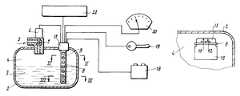
- FIG. 1shows the liquefied-petroleum-gas tank of a vehicle, equipped with a device per this invention together with its connections to various functional components of the vehicle;
- FIGS. 2 and 3represent two cross-sectional views of an optical detector respectively outside and inside the liquefied petroleum gas along lines II—II and III—III in FIG. 1;
- FIGS. 4 and 5respectively represent an exploded and an assembled view of the fill-level indicator according to this invention.
- FIG. 6is an exploded perspective view of a device per this invention and a corresponding retaining head
- FIG. 7shows a cross-section through a detector
- FIG. 8is an exploded perspective view, on an enlarged scale, of the free end of the device per FIG. 6 .
- FIG. 1illustrates a liquefied-petroleum-gas tank 2 designed for use in an automobile. Above the liquid gas 3 contained in the tank is a gaseous volume 4 .
- the tankis equipped with an essentially conventional filler unit 5 , mounted on which is a solenoid valve 6 that operates a flap 7 which depending on its position permits or blocks the filling of the tank
- the fill-level indicatorincorporates a bar 8 which, in the implementation shown in the drawing, extends vertically inside the tank.
- This barholds an array of detectors 9 each of which includes a light source 10 consisting for instance of a visible- or infrared-range light-emitting diode, and a receiver 12 consisting of a photoelectric cell or a photothyristor.
- the bar 8may be in the form for instance of a printed circuit board.
- the various detectors 9are attached to the bar 8 which serves as a mount and is encased in a synthetic resin 13 whose refractive index is close to the refractive index of the liquid gas.
- the optical axes of the light source 10 and the corresponding receiver 12are parallel.
- the light source 10 and the receiverare close together and the surface of the resin 13 facing the detector 9 extends parallel to the mount 8 constituted of the flat printed circuit board.
- the light beam emanating from the source 10is reflected and directed toward the receiver 12 .
- the result as shown in FIG. 2will be a nearly total reflection of the light beam toward the receiver 12 , with the refractive index of the gas 4 being well below the index of the resin.
- a detectoris immersed in liquid gas, most of the light beam emitted by the source 10 is diffracted within the liquid gas 3 , with the refractive indices of the liquid and of the resin 13 being very similar.
- the analysis of the signals emitted by the different receivers 12 of the detectors 9permits the determination of which detectors are immersed and which are not, and thus a measurement of the fill-level of the liquid.
- one approach to implementing a fill-level indicatoris to insert a bar 8 with detectors 9 in a casing 16 in the form of a U-shaped trough.
- the casing 16is then filled with a synthetic material that is transparent to the light beam while perfectly insulating the detectors 9 as well as their power-supply and signal-acquisition elements from the liquid and gaseous fluids in the tank 2 .
- An example of such synthetic materialis epoxy resin.
- the casing 16is a channel with a U-shaped cross section. It thus has two legs 23 and a base 24 . Each leg 23 is provided on its inside with a groove 25 that extends longitudinally over the entire length of the casing 16 .
- the two grooves 25are so designed that the printed circuit board mount 8 can slide and be guided in them and can be positioned parallel to the base 24 of the casing.
- the lattermay be produced for instance of polycarbonate.
- the printed circuit board 8is inserted in the casing 16 in such fashion that the detectors 9 face the base of the casing and are perfectly parallel to it.
- the casingis inserted in flush fashion in a retaining head 26 .
- This retaining headmade of metal, is attached to the tank with four screws via an annular flange, not shown, in the location usually serving to accept a conventional mechanical float-based gauge.
- the metal head 26absorbs the pressure exerted by the LPG in the tank 2 .
- a cavity 27 matching the shape of the casingis provided in the retaining head 26 in such fashion that the head is translationally locked in place as the gas pressure bears on it.
- a fastening hole 32serves to secure the casing 16 on the retaining head 26 .
- An insulated wire conduit 28 through which extend metal pins 29is mounted in the retaining head 26 , serving as the terminal pin connection.
- the male pin connectorsthus protrude from the head 26 to the outside of the tank. They connect to an electronics box 17 which will be described further below. This link to the electronics box 17 is established for instance by means of female connectors, not shown, or by wires soldered to the male pin connectors, and is then potted in epoxy resin, sealing the assembly.
- the probeis laid sideways for encapsulation in epoxy resin which is applied by simple gravitational flow.
- the resinis carefully selected for its transparency to the emitted light beam and its compatibility with the LPG while at the same time ensuring good mechanical qualities in terms of hardness, electrical insulation and thermal resistance after polymerization.
- the end of the casing 16 opposite the retaining head 26is covered with a lid 30 which tightly closes off the end of the casing. A space is left between the mount 8 and the lid 30 to allow the epoxy resin to flow on both sides of the mount 8 .
- the resinseals the assembly into a single solid block, galvanically insulating the electric currents from the LPG.
- the resinensures perfect tightness of the casing and of the wire conduit in the head of the probe.
- the horizontal pouring processpermits substantial elimination of microbubbles within the resin, bubbles which could interfere with the optical path of the light beam emitted by a light source 10 of the detector 9 .
- the base 24 of the casing 16Since the light sources 10 are very close to the receivers 12 , the base 24 of the casing 16 must be flat. The distance between the detectors 9 and the base 24 of the casing, i.e. the thickness of the resin layer 13 covering the detectors 9 , must be kept minimal so as to minimize any deviation of the light path on the flat surface.
- the casingcould conceivably be removed to leave only a block of resin 13 surrounding the mount 8 and the detectors 9 .
- the casingeven if the refractive indices of the resin and of the material constituting the casing are very close (about 1.5 to 1.6), the presence of a diopter between the resin and the casing causes a deviation of the light beam. Therefore, any such diopter should preferably be avoided.
- FIG. 7which is a cross-sectional view of a probe without a casing. The result is a mount 8 with detectors 9 , as shown in FIGS. 2 and 3, encapsulated in a block of resin 13 .
- the bar 8connects to an electronics box 17 .
- This boxon its part is connected to the battery 18 of the vehicle, to the distribution panel 19 permitting electric current to be fed to the engine, to the fuel fill-level display gauge 20 on the vehicle dashboard, and to the electronic engine fuel injection system 22 .
- the electronics box 17possibly comprising a microprocessor or microcontroller, feeds power from the battery 18 to the diodes 10 which constitute the light sources.
- This box 17performs various signal processing functions aimed both at providing a readout of the liquid gas level in the tank and at assuring a safe installation.
- the probedelivers only discontinuous measurements.
- a smoothing functionis provided which permits a gradual decline of the needle by simulating intermediate measurements between two actual measuring points, with an interpolation of a mean gas consumption value over an average length of time.
- the smoothing functionis reset for the change of state of each detector.
- the box 17also ensures a filtering of sudden changes of state of the detectors by integrating a time delay during which detection variations will not register.
- the bottom-most detectorwhen immersed in the liquid, sends to the electronics box 17 a signal permitting it, for example, to initiate the automatic switchover to gasoline for fueling the engine.
- the tankFor safety reasons and especially in order to allow for an increased pressure of the gaseous phase in higher temperature conditions, the tank must not be filled more than 80% of its total capacity. It is therefore possible to install a maximum-level detector which, when activated by a high level of liquid, sends a signal to the electronics box on the basis of which the latter can instruct the solenoid valve 6 to ensure the closure of the filler unit.
- the electronics box 17is also connected to the distribution panel 19 for the purpose of preventing the filling of the tank while the engine of the vehicle is running.
- the detectors 9are mounted at space intervals carefully chosen in consideration of the shape of the tank. Accordingly, they are closer together in the bottom part of the tank to assure greater measurement accuracy as the liquid level approaches the fuel “reserve”. This irregular placement of the detectors permits employing the same signal processing electronics regardless of the type of tank.
- the optical probe itself(the detectors encapsulated in resin) is specifically adapted to each type of tank while the signal processing module (measurement interpretation, smoothing, actuator control, message to the dashboard gauge, etc.) remains the same for all models, thus considerably reducing manufacturing costs.
- the electronics box 17ultimately ensures automatic control of the detectors by sending a signal in the event one of the detectors is malfunctioning. If the maximum-fill-level detector fails, its functions are immediately transferred to the next lower detector. As an alternative, the microcontroller or microprocessor can interdict any refilling while that detector is failing by keeping the solenoid valve closed.
- this inventionconstitutes a major improvement on the state of the art by providing a fill-level indicator for liquefied petroleum gas tanks that is compact, has no moving parts, is not affected by normal pressure or temperature fluctuations in the range respectively from 0 to 30 bars and minus 20° C. to plus 65° C., while offering excellent accuracy and outstanding reliability.
Landscapes
- Physics & Mathematics (AREA)
- Electromagnetism (AREA)
- Thermal Sciences (AREA)
- Fluid Mechanics (AREA)
- General Physics & Mathematics (AREA)
- Measurement Of Levels Of Liquids Or Fluent Solid Materials (AREA)
Abstract
Description
This invention relates to a fill level indicator for use in a liquefied-petroleum-gas tank. The device is particularly suitable for indicating the fill level of an automobile fuel tank.
In the case of a liquefied-petroleum-gas tank it is important to precisely monitor fill-level changes. In fact, because of fuel expansion, safety considerations dictate that the tank not be filled more than 80% of its total capacity. At the low level a tank must also provide information that allows for instance a switchover to gasoline for fueling the engine.
The gauges that have been employed to date are based on a mechanical float system which has numerous drawbacks including in particular imprecise measurements due to mechanical slack, the risk of malfunction of the mechanical elements due to seizing or wear as they age, random measurement variations due to vehicle movements, the difficulty of compartmentalizing a liquefied gas tank for limiting the movement of the fluid as in the case of a gasoline tank, their bulk in the tank, and the lack of safety.
There exist gauges which incorporate optical detection devices whose operation is based on measuring the difference in the refractive index between liquid and gaseous substances. The U.S. Pat. No. 4,286,464 describes such a fill-level indicator in a tank and especially in an oil reservoir. The fill-level indicator described in that document incorporates an array of vertically staggered optical detectors. Each detector includes a light source such as a gallium and arsenic P-N LED, a receiver such as a flat P-N-P silicon phototransistor, as well as light-beam transmitting elements. These elements transmit the beam from the light source to the receiver when the detector is out of the liquid while the beam is refracted when the detector is immersed in the liquid. Electronic circuitry permits the transmission of the signals received by the detectors to an oil-level display gauge.
It is the objective of this invention to provide a fill-level indicator for liquefied petroleum gas tanks which indicator is compact, has no moving parts, is highly reliable and can be coupled to additional safety provisions such as a fill lock which is enabled when a certain level is reached or when the engine of the vehicle is running.
The device is designed to employ optical detectors whose detection principle is based on the difference in the refractive index between liquid and gaseous substances.
Accordingly, the indicator presented incorporates the following:
An array of optical detectors on a mount, vertically spaced apart from one another inside the tank and distributed over the height of the tank, with each detector encompassing a light source and a receiver, and
Means which power the light sources of the various detectors, process the information received from the different detectors and transmit it to a liquefied-gas fill-level display gauge.
According to the invention, the mount and the detectors on it are enclosed in a synthetic resin that is highly transparent to the light beams emitted by the light sources while the surface of the resin facing the detectors is such that a light beam emitted by the corresponding light source is reflected toward the associated receiver.
This design concept permits the use of optical detectors in a liquefied petroleum gas (LPG) tank in which the ambient conditions are particularly severe. With the resin it is possible to seal the sensor assembly into one solid, single block, providing excellent electrical insulation of these components from the LPG.
The level of the gas inside the tank is measured by processing the signals that have reached the different receivers, based on the fact that each of the receivers positioned in the gaseous phase receives a light beam emitted by the corresponding light source, whereas the other receivers, i.e. those immersed in liquid gas, do not receive such signals.
In one design implementation of this device, each light source consists of a diode which emits a light beam in the visible or infrared wavelength range and each receiver is constituted of a photoelectric cell or a photothyristor.
The resin used may for instance be an epoxy, given that it has a refractive index close to that of the LPG in the liquid phase.
When a detector is positioned in the gaseous phase, the emitted light beam is reflected toward the corresponding receiver since the index of the gas, at close to 1, is optically well below the index of the resin.
When the detector is positioned in the liquid phase, the beam emitted by the light source is essentially diffused in the liquid since the refractive indices of the liquid and of the resin are similar at about 1.3 to 1.4. A small part of the light beam may still be reflected toward the receiver, but the sensitivity of the latter is not such as to register light of this weak a magnitude.
The section of the resin layer covering the detectors is not contour-matched since it is important that the light path of the beam reflected by the inner wall surface of the resin be directed from the light source toward the detector. However, it is desirable to place the light source and the receiver of a given detector quite close together and to have the surface of the resin in front of the detector assembly, composed of light source and sensor, extend parallel to the detector and its mount.
In a design variation, the mount is located in a casing that serves as an outer enclosure for the resin and is highly transparent to the beams emitted by the light sources. This casing may consist for instance of polycarbonate. The refractive index of the material constituting the casing must be as close as possible to the index of the resin and of the LPG in the liquid phase.
The casing is preferably U-shaped. Each leg of the U is provided, for instance on its inner surface, with a longitudinal groove and the two grooves serve to accept the detector mount in such fashion that it extends parallel to the base of the casing. The detector mount is thus perfectly aligned in the casing, providing good parallelism between the base plane of the casing and the plane of the detector mount. Of course, surfaces other than these planar surfaces can be utilized for the base and the mount, but the planar configuration offers the advantage of being the easiest to implement.
For fitting the probe in the tank containing the LPG, the mount, the resin and possibly the casing are enclosed in a retaining head that is attached to the tank. This retaining head may for instance be a metal head equipped with an annular flange and bolted to the tank. This allows the heed to be mounted in the location usually occupied by a traditional float-type mechanical gauge, fastened to the tank with four screws.
To ensure proper electrical connection between the detectors of the probe and the outside of the tank, an insulated wire conduit is suitably installed in the retaining head.
According to one advantageous embodiment of the indicator per this invention, the mount supporting the detectors consists of a printed circuit board.
In a preferred design implementation the means for supplying electric power to the light sources and for processing the signals include a microprocessor or microcontroller.
Since the fill-level indicator only provides discrete i.e. discontinuous measurements, it will be desirable to prevent the needle of the gauge from dropping upon every change of the state of a detector. This is accomplished in that the signal processing means perform a smoothing function on the value of the gauge shift between the corresponding measurements of two neighboring detectors, simulating intermediate measurements between two actual measuring points by the interpolation of a mean gas consumption value during an average time period.
To avoid registering every interference-induced change in the state of the detectors which does not reflect the actual level of the liquid, caused by the splashing of droplets, a wave motion due to movements of the vehicle or a leaning of the vehicle, the signal processing elements include a change-of-state filtering provision for the detectors which establishes a time period during which no variation in the detection is to be registered. This time period can be relatively short, with a duration on the order of a few seconds, depending on the desired sensitity level.
As an advantageous feature of this invention when applied to an automobile tank, the signal processing means are connected at one end to the electric distribution panel of the vehicle engine and at the other end to a solenoid valve installed on the tank filler inlet, enabling the solenoid valve to open up only when the engine is stopped and when the fluid is below a specific level, the maximum fill level being 80% of the tank capacity which corresponds to the position of the uppermost detector.
The device per this invention thus incorporates important safety functions. It should be noted that in conventional systems the overfill prevention is implemented by mechanical means employing a float, which again has the same shortcomings as those mentioned above in connection with the gauge.
To ensure highly safe operation of the device, the signal processing means include for instance a test function for all optical detectors and for the various electronic components which may be subject to possible malfunction.
For safety reasons, if the maximum-fill detector were to fail, its functions are automatically transferred to the next lower detector, or the filler solenoid valve remains closed.
The signal processing means which include a microcontroller or a microprocessor may also be designed in a way as to reduce electric power consumption when idle, i.e. when the vehicle is stopped, or to conserve the power for retaining control of the solenoid valve in the fill position. It is possible to provide these signal processing elements with an interface to the electronic fuel injection system for the purpose of enhanced performance and safety of the vehicle.
This invention will be better understood with the aid of the following description with reference to the attached drawings, illustrating non-limiting examples of several forms of implementation of this device.
FIG. 1 shows the liquefied-petroleum-gas tank of a vehicle, equipped with a device per this invention together with its connections to various functional components of the vehicle;
FIGS. 2 and 3 represent two cross-sectional views of an optical detector respectively outside and inside the liquefied petroleum gas along lines II—II and III—III in FIG. 1;
FIGS. 4 and 5 respectively represent an exploded and an assembled view of the fill-level indicator according to this invention;
FIG. 6 is an exploded perspective view of a device per this invention and a corresponding retaining head;
FIG. 7 shows a cross-section through a detector; and
FIG. 8 is an exploded perspective view, on an enlarged scale, of the free end of the device per FIG.6.
FIG. 1 illustrates a liquefied-petroleum-gas tank 2 designed for use in an automobile. Above theliquid gas 3 contained in the tank is agaseous volume 4. The tank is equipped with an essentiallyconventional filler unit 5, mounted on which is asolenoid valve 6 that operates a flap7 which depending on its position permits or blocks the filling of the tank
The fill-level indicator incorporates abar 8 which, in the implementation shown in the drawing, extends vertically inside the tank. This bar holds an array ofdetectors 9 each of which includes alight source 10 consisting for instance of a visible- or infrared-range light-emitting diode, and areceiver 12 consisting of a photoelectric cell or a photothyristor. Thebar 8 may be in the form for instance of a printed circuit board. Thevarious detectors 9 are attached to thebar 8 which serves as a mount and is encased in asynthetic resin 13 whose refractive index is close to the refractive index of the liquid gas. In the implementation per FIGS. 2 and 3 the optical axes of thelight source 10 and the correspondingreceiver 12 are parallel. Thelight source 10 and the receiver are close together and the surface of theresin 13 facing thedetector 9 extends parallel to themount 8 constituted of the flat printed circuit board. Correspondingly, the light beam emanating from thesource 10 is reflected and directed toward thereceiver 12. When the detector is positioned in thegaseous phase 4, the result as shown in FIG. 2 will be a nearly total reflection of the light beam toward thereceiver 12, with the refractive index of thegas 4 being well below the index of the resin. By contrast, when, as shown in FIG.3 and represented by the intersecting line III—III in FIG. 1, a detector is immersed in liquid gas, most of the light beam emitted by thesource 10 is diffracted within theliquid gas 3, with the refractive indices of the liquid and of theresin 13 being very similar.
The analysis of the signals emitted by thedifferent receivers 12 of thedetectors 9 permits the determination of which detectors are immersed and which are not, and thus a measurement of the fill-level of the liquid.
As shown in FIGS. 4 to8, one approach to implementing a fill-level indicator is to insert abar 8 withdetectors 9 in acasing 16 in the form of a U-shaped trough. Thecasing 16 is then filled with a synthetic material that is transparent to the light beam while perfectly insulating thedetectors 9 as well as their power-supply and signal-acquisition elements from the liquid and gaseous fluids in thetank 2. An example of such synthetic material is epoxy resin.
Thecasing 16 is a channel with a U-shaped cross section. It thus has twolegs 23 and abase 24. Eachleg 23 is provided on its inside with agroove 25 that extends longitudinally over the entire length of thecasing 16. The twogrooves 25 are so designed that the printedcircuit board mount 8 can slide and be guided in them and can be positioned parallel to thebase 24 of the casing. The latter may be produced for instance of polycarbonate. The printedcircuit board 8 is inserted in thecasing 16 in such fashion that thedetectors 9 face the base of the casing and are perfectly parallel to it.
Thus assembled, the casing is inserted in flush fashion in a retaininghead 26. This retaining head, made of metal, is attached to the tank with four screws via an annular flange, not shown, in the location usually serving to accept a conventional mechanical float-based gauge. Themetal head 26 absorbs the pressure exerted by the LPG in thetank 2. Acavity 27 matching the shape of the casing is provided in the retaininghead 26 in such fashion that the head is translationally locked in place as the gas pressure bears on it. Afastening hole 32 serves to secure thecasing 16 on the retaininghead 26.
Aninsulated wire conduit 28 through which extendmetal pins 29 is mounted in the retaininghead 26, serving as the terminal pin connection. The male pin connectors thus protrude from thehead 26 to the outside of the tank. They connect to anelectronics box 17 which will be described further below. This link to theelectronics box 17 is established for instance by means of female connectors, not shown, or by wires soldered to the male pin connectors, and is then potted in epoxy resin, sealing the assembly.
After all these components are assembled, the probe is laid sideways for encapsulation in epoxy resin which is applied by simple gravitational flow. The resin is carefully selected for its transparency to the emitted light beam and its compatibility with the LPG while at the same time ensuring good mechanical qualities in terms of hardness, electrical insulation and thermal resistance after polymerization. As shown in FIG. 8, for pouring the resin the end of thecasing 16 opposite the retaininghead 26 is covered with alid 30 which tightly closes off the end of the casing. A space is left between themount 8 and thelid 30 to allow the epoxy resin to flow on both sides of themount 8.
The resulting trough is completely filled horizontally. When polymerized, the resin seals the assembly into a single solid block, galvanically insulating the electric currents from the LPG. In addition, the resin ensures perfect tightness of the casing and of the wire conduit in the head of the probe.
The horizontal pouring process permits substantial elimination of microbubbles within the resin, bubbles which could interfere with the optical path of the light beam emitted by alight source 10 of thedetector 9.
Since thelight sources 10 are very close to thereceivers 12, thebase 24 of thecasing 16 must be flat. The distance between thedetectors 9 and thebase 24 of the casing, i.e. the thickness of theresin layer 13 covering thedetectors 9, must be kept minimal so as to minimize any deviation of the light path on the flat surface.
To reduce possible interference with the transmission of the light beam to a minimum, the casing could conceivably be removed to leave only a block ofresin 13 surrounding themount 8 and thedetectors 9. In fact, with the casing, even if the refractive indices of the resin and of the material constituting the casing are very close (about 1.5 to 1.6), the presence of a diopter between the resin and the casing causes a deviation of the light beam. Therefore, any such diopter should preferably be avoided. This leads to an implementation as shown in FIG. 7 which is a cross-sectional view of a probe without a casing. The result is amount 8 withdetectors 9, as shown in FIGS. 2 and 3, encapsulated in a block ofresin 13.
As indicated in FIG. 1, thebar 8 connects to anelectronics box 17. This box on its part is connected to thebattery 18 of the vehicle, to thedistribution panel 19 permitting electric current to be fed to the engine, to the fuel fill-level display gauge 20 on the vehicle dashboard, and to the electronic enginefuel injection system 22. Theelectronics box 17, possibly comprising a microprocessor or microcontroller, feeds power from thebattery 18 to thediodes 10 which constitute the light sources. Thisbox 17 performs various signal processing functions aimed both at providing a readout of the liquid gas level in the tank and at assuring a safe installation.
Note that the probe delivers only discontinuous measurements. To avoid having the needle of thegauge 20 drop every time there is a change in state of a detector, a smoothing function is provided which permits a gradual decline of the needle by simulating intermediate measurements between two actual measuring points, with an interpolation of a mean gas consumption value over an average length of time. The smoothing function is reset for the change of state of each detector.
Thebox 17 also ensures a filtering of sudden changes of state of the detectors by integrating a time delay during which detection variations will not register.
The bottom-most detector, when immersed in the liquid, sends to the electronics box17 a signal permitting it, for example, to initiate the automatic switchover to gasoline for fueling the engine.
For safety reasons and especially in order to allow for an increased pressure of the gaseous phase in higher temperature conditions, the tank must not be filled more than 80% of its total capacity. It is therefore possible to install a maximum-level detector which, when activated by a high level of liquid, sends a signal to the electronics box on the basis of which the latter can instruct thesolenoid valve 6 to ensure the closure of the filler unit. Theelectronics box 17 is also connected to thedistribution panel 19 for the purpose of preventing the filling of the tank while the engine of the vehicle is running.
Thedetectors 9 are mounted at space intervals carefully chosen in consideration of the shape of the tank. Accordingly, they are closer together in the bottom part of the tank to assure greater measurement accuracy as the liquid level approaches the fuel “reserve”. This irregular placement of the detectors permits employing the same signal processing electronics regardless of the type of tank. The optical probe itself (the detectors encapsulated in resin) is specifically adapted to each type of tank while the signal processing module (measurement interpretation, smoothing, actuator control, message to the dashboard gauge, etc.) remains the same for all models, thus considerably reducing manufacturing costs.
Theelectronics box 17 ultimately ensures automatic control of the detectors by sending a signal in the event one of the detectors is malfunctioning. If the maximum-fill-level detector fails, its functions are immediately transferred to the next lower detector. As an alternative, the microcontroller or microprocessor can interdict any refilling while that detector is failing by keeping the solenoid valve closed.
Turning off the engine triggers the opening of the solenoid valve on the filler unit for a duration τ. If during that time period τ the 80% maximum-fill-level detector or the engine starter are not used, a delay device causes the solenoid valve to close.
As will be evident from the above, this invention constitutes a major improvement on the state of the art by providing a fill-level indicator for liquefied petroleum gas tanks that is compact, has no moving parts, is not affected by normal pressure or temperature fluctuations in the range respectively from 0 to 30 bars and minus 20° C. to plus 65° C., while offering excellent accuracy and outstanding reliability.
It goes without saying that this invention is not limited to the design implementations described above by way of examples but, on the contrary, it embraces all possible variations. Specifically, the number of detectors may differ, their placement in the tank may differ, and the shape of the casing associated with the detectors may differ, without departing from the substance of this invention.
Claims (14)
1. Fill-level indicator for use in a liquefied petroleum gas tank, comprising:
an array of optical detectors attached to a mount, vertically spaced apart from one another and distributed inside the tank over a height of the tank, each detector including a light source and a receiver, and
means for feeding power to the light sources of the various detectors, for processing signals arriving at the various receivers and for transmitting signals to a gauge displaying a fill-level of the liquefied gas,
wherein the mount and the detectors placed thereon are positioned in a casing which is highly transparent to light beams emitted by the light sources and wherein a synthetic resin which is highly transparent to the light beams emitted by the light sources is disposed between one surface of the casing and the detectors for encapsulating the mount and the detectors such that a surface of the resin facing the detectors reflects a light beam emitted by the corresponding light source toward the associated receiver, and
wherein the casing comprises a material having a refractive index very close to that of the resin.
2. Fill-level indicator as inclaim 1 , wherein when used in an automobile tank, the means for feeding power and for processing the signals is connected at one end to a distribution panel for feeding electric current to an engine of a vehicle and at the other end to a solenoid valve mounted on a filler unit of the tank, for permitting the opening of the solenoid valve only when the engine is stopped and the fill level is below a specific point, and wherein about 80% of a maximum capacity of the tank is represented by the detector in an uppermost position.
3. Fill-level indicator as inclaim 1 , wherein the resin is an epoxy resin.
4. Fill-level indicator as inclaim 1 , wherein the casing comprises polycarbonate.
5. Fill-level indicator as inclaim 1 , wherein the casing is in the form of a U-shaped profile, legs of the U each including on an inside thereof a longitudinal groove, whereby the grooves accept the mount with the detectors such that the mount extends parallel to a base of the casing.
6. Fill-level indicator as inclaim 1 , wherein the mount, the resin and the casing are flush-mounted in a retaining head designed to be attached to the tank.
7. Fill-level indicator as inclaim 6 , wherein the retaining head is a metal head equipped with an annular flange and attached to the tank.
8. Fill-level indicator as inclaim 6 , wherein an insulated wire conduit is installed in the retaining head.
9. Fill-level indicator as inclaim 1 , wherein the mount comprises a printed circuit board.
10. Fill-level indicator as inclaim 1 , wherein the means for feeding power to the light sources and for processing the signals include a microprocessor or a microcontroller.
11. Fill-level indicator as inclaim 1 , wherein the means for feeding power and for processing the signals performs a smoothing of a shift value of the gauge between measurements of two neighboring detectors by simulating intermediate measurements between two actual measuring points, interpolating a mean gas consumption during an average time period.
12. Fill-level indicator as in claims1, wherein the means for feeding power and for processing the signals includes a filtering of the change of state of the detectors by integration of a time lag during which no detection variation is to be registered.
13. Fill-level indicator as inclaim 1 , wherein the means for feeding power and for processing the signals performs a detector test function within a specific periodic cycle.
14. Fill-level indicator as inclaim 13 , wherein in the event of a failure of a maximum-fill-level detector functions of the maximum fill-level detector are automatically transferred to a next lower detector, or filling of the tank is rendered impossible by keeping a solenoid valve closed.
Priority Applications (1)
| Application Number | Priority Date | Filing Date | Title |
|---|---|---|---|
| US09/888,038US6658933B2 (en) | 2001-06-22 | 2001-06-22 | Fill-level indicator for a liquefied-petroleum-gas tank |
Applications Claiming Priority (1)
| Application Number | Priority Date | Filing Date | Title |
|---|---|---|---|
| US09/888,038US6658933B2 (en) | 2001-06-22 | 2001-06-22 | Fill-level indicator for a liquefied-petroleum-gas tank |
Publications (2)
| Publication Number | Publication Date |
|---|---|
| US20020194911A1 US20020194911A1 (en) | 2002-12-26 |
| US6658933B2true US6658933B2 (en) | 2003-12-09 |
Family
ID=25392398
Family Applications (1)
| Application Number | Title | Priority Date | Filing Date |
|---|---|---|---|
| US09/888,038Expired - Fee RelatedUS6658933B2 (en) | 2001-06-22 | 2001-06-22 | Fill-level indicator for a liquefied-petroleum-gas tank |
Country Status (1)
| Country | Link |
|---|---|
| US (1) | US6658933B2 (en) |
Cited By (238)
| Publication number | Priority date | Publication date | Assignee | Title |
|---|---|---|---|---|
| US6968739B1 (en)* | 2004-06-04 | 2005-11-29 | Joseph Baron | Gauge and method for indicating a level of a liquid in a tank |
| US20050263186A1 (en)* | 2003-09-30 | 2005-12-01 | C.R.F. Societa Consortile Per Azioni | System for controlling filling of a motor-vehicle tank with LPG, and a servo valve used therein |
| US20060191826A1 (en)* | 2005-02-04 | 2006-08-31 | Davco Technology, L.L.C. | Apparatus and method for determining a fluid level within an enclosed container |
| US20060231138A1 (en)* | 2005-03-29 | 2006-10-19 | Stant Manufacturing Inc. | Electronic fuel tank fill limit control |
| US20110221803A1 (en)* | 2009-01-09 | 2011-09-15 | Mimaki Engineering Co., Ltd. | Ink supply apparatus |
| US20120138824A1 (en)* | 2010-12-03 | 2012-06-07 | Fang Wen | Continuous liquid level sensor having multiple light sources and light receiving devices |
| US20130030677A1 (en)* | 2010-03-09 | 2013-01-31 | Wacker Neuson Produktion GmbH & Co. KG | Drive system with an apparatus for interrupting the operation in the case of an imminent lack of operating medium |
| US20160123779A1 (en)* | 2014-10-29 | 2016-05-05 | Siemens Schweiz Ag | Cover For A Duct Sensor |
| US11274369B2 (en) | 2018-09-11 | 2022-03-15 | Asm Ip Holding B.V. | Thin film deposition method |
| US11286558B2 (en) | 2019-08-23 | 2022-03-29 | Asm Ip Holding B.V. | Methods for depositing a molybdenum nitride film on a surface of a substrate by a cyclical deposition process and related semiconductor device structures including a molybdenum nitride film |
| USD947913S1 (en) | 2019-05-17 | 2022-04-05 | Asm Ip Holding B.V. | Susceptor shaft |
| US11296189B2 (en) | 2018-06-21 | 2022-04-05 | Asm Ip Holding B.V. | Method for depositing a phosphorus doped silicon arsenide film and related semiconductor device structures |
| US11295980B2 (en) | 2017-08-30 | 2022-04-05 | Asm Ip Holding B.V. | Methods for depositing a molybdenum metal film over a dielectric surface of a substrate by a cyclical deposition process and related semiconductor device structures |
| US11306395B2 (en) | 2017-06-28 | 2022-04-19 | Asm Ip Holding B.V. | Methods for depositing a transition metal nitride film on a substrate by atomic layer deposition and related deposition apparatus |
| US11315794B2 (en) | 2019-10-21 | 2022-04-26 | Asm Ip Holding B.V. | Apparatus and methods for selectively etching films |
| US11342216B2 (en) | 2019-02-20 | 2022-05-24 | Asm Ip Holding B.V. | Cyclical deposition method and apparatus for filling a recess formed within a substrate surface |
| US11339476B2 (en) | 2019-10-08 | 2022-05-24 | Asm Ip Holding B.V. | Substrate processing device having connection plates, substrate processing method |
| US11345999B2 (en) | 2019-06-06 | 2022-05-31 | Asm Ip Holding B.V. | Method of using a gas-phase reactor system including analyzing exhausted gas |
| US11355338B2 (en) | 2019-05-10 | 2022-06-07 | Asm Ip Holding B.V. | Method of depositing material onto a surface and structure formed according to the method |
| US11361990B2 (en) | 2018-05-28 | 2022-06-14 | Asm Ip Holding B.V. | Substrate processing method and device manufactured by using the same |
| US11378337B2 (en) | 2019-03-28 | 2022-07-05 | Asm Ip Holding B.V. | Door opener and substrate processing apparatus provided therewith |
| US11387106B2 (en) | 2018-02-14 | 2022-07-12 | Asm Ip Holding B.V. | Method for depositing a ruthenium-containing film on a substrate by a cyclical deposition process |
| US11387120B2 (en) | 2017-09-28 | 2022-07-12 | Asm Ip Holding B.V. | Chemical dispensing apparatus and methods for dispensing a chemical to a reaction chamber |
| US11390950B2 (en) | 2017-01-10 | 2022-07-19 | Asm Ip Holding B.V. | Reactor system and method to reduce residue buildup during a film deposition process |
| US11390946B2 (en) | 2019-01-17 | 2022-07-19 | Asm Ip Holding B.V. | Methods of forming a transition metal containing film on a substrate by a cyclical deposition process |
| US11393690B2 (en) | 2018-01-19 | 2022-07-19 | Asm Ip Holding B.V. | Deposition method |
| US11390945B2 (en) | 2019-07-03 | 2022-07-19 | Asm Ip Holding B.V. | Temperature control assembly for substrate processing apparatus and method of using same |
| US11396702B2 (en) | 2016-11-15 | 2022-07-26 | Asm Ip Holding B.V. | Gas supply unit and substrate processing apparatus including the gas supply unit |
| US11398382B2 (en) | 2018-03-27 | 2022-07-26 | Asm Ip Holding B.V. | Method of forming an electrode on a substrate and a semiconductor device structure including an electrode |
| US11401605B2 (en) | 2019-11-26 | 2022-08-02 | Asm Ip Holding B.V. | Substrate processing apparatus |
| US11411088B2 (en) | 2018-11-16 | 2022-08-09 | Asm Ip Holding B.V. | Methods for forming a metal silicate film on a substrate in a reaction chamber and related semiconductor device structures |
| US11410851B2 (en) | 2017-02-15 | 2022-08-09 | Asm Ip Holding B.V. | Methods for forming a metallic film on a substrate by cyclical deposition and related semiconductor device structures |
| US11414760B2 (en) | 2018-10-08 | 2022-08-16 | Asm Ip Holding B.V. | Substrate support unit, thin film deposition apparatus including the same, and substrate processing apparatus including the same |
| US11417545B2 (en) | 2017-08-08 | 2022-08-16 | Asm Ip Holding B.V. | Radiation shield |
| US11424119B2 (en) | 2019-03-08 | 2022-08-23 | Asm Ip Holding B.V. | Method for selective deposition of silicon nitride layer and structure including selectively-deposited silicon nitride layer |
| US11430674B2 (en) | 2018-08-22 | 2022-08-30 | Asm Ip Holding B.V. | Sensor array, apparatus for dispensing a vapor phase reactant to a reaction chamber and related methods |
| US11430640B2 (en) | 2019-07-30 | 2022-08-30 | Asm Ip Holding B.V. | Substrate processing apparatus |
| US11437241B2 (en) | 2020-04-08 | 2022-09-06 | Asm Ip Holding B.V. | Apparatus and methods for selectively etching silicon oxide films |
| US11443926B2 (en) | 2019-07-30 | 2022-09-13 | Asm Ip Holding B.V. | Substrate processing apparatus |
| US11447864B2 (en) | 2019-04-19 | 2022-09-20 | Asm Ip Holding B.V. | Layer forming method and apparatus |
| US11450529B2 (en) | 2019-11-26 | 2022-09-20 | Asm Ip Holding B.V. | Methods for selectively forming a target film on a substrate comprising a first dielectric surface and a second metallic surface |
| US11447861B2 (en) | 2016-12-15 | 2022-09-20 | Asm Ip Holding B.V. | Sequential infiltration synthesis apparatus and a method of forming a patterned structure |
| US11453943B2 (en) | 2016-05-25 | 2022-09-27 | Asm Ip Holding B.V. | Method for forming carbon-containing silicon/metal oxide or nitride film by ALD using silicon precursor and hydrocarbon precursor |
| USD965044S1 (en) | 2019-08-19 | 2022-09-27 | Asm Ip Holding B.V. | Susceptor shaft |
| USD965524S1 (en) | 2019-08-19 | 2022-10-04 | Asm Ip Holding B.V. | Susceptor support |
| US11476109B2 (en) | 2019-06-11 | 2022-10-18 | Asm Ip Holding B.V. | Method of forming an electronic structure using reforming gas, system for performing the method, and structure formed using the method |
| US11473195B2 (en) | 2018-03-01 | 2022-10-18 | Asm Ip Holding B.V. | Semiconductor processing apparatus and a method for processing a substrate |
| US11482412B2 (en) | 2018-01-19 | 2022-10-25 | Asm Ip Holding B.V. | Method for depositing a gap-fill layer by plasma-assisted deposition |
| US11482533B2 (en) | 2019-02-20 | 2022-10-25 | Asm Ip Holding B.V. | Apparatus and methods for plug fill deposition in 3-D NAND applications |
| US11482418B2 (en) | 2018-02-20 | 2022-10-25 | Asm Ip Holding B.V. | Substrate processing method and apparatus |
| US11488854B2 (en) | 2020-03-11 | 2022-11-01 | Asm Ip Holding B.V. | Substrate handling device with adjustable joints |
| US11488819B2 (en) | 2018-12-04 | 2022-11-01 | Asm Ip Holding B.V. | Method of cleaning substrate processing apparatus |
| US11492703B2 (en) | 2018-06-27 | 2022-11-08 | Asm Ip Holding B.V. | Cyclic deposition methods for forming metal-containing material and films and structures including the metal-containing material |
| US11495459B2 (en) | 2019-09-04 | 2022-11-08 | Asm Ip Holding B.V. | Methods for selective deposition using a sacrificial capping layer |
| US11499226B2 (en) | 2018-11-02 | 2022-11-15 | Asm Ip Holding B.V. | Substrate supporting unit and a substrate processing device including the same |
| US11501973B2 (en) | 2018-01-16 | 2022-11-15 | Asm Ip Holding B.V. | Method for depositing a material film on a substrate within a reaction chamber by a cyclical deposition process and related device structures |
| US11501968B2 (en) | 2019-11-15 | 2022-11-15 | Asm Ip Holding B.V. | Method for providing a semiconductor device with silicon filled gaps |
| US11499222B2 (en) | 2018-06-27 | 2022-11-15 | Asm Ip Holding B.V. | Cyclic deposition methods for forming metal-containing material and films and structures including the metal-containing material |
| US11515188B2 (en) | 2019-05-16 | 2022-11-29 | Asm Ip Holding B.V. | Wafer boat handling device, vertical batch furnace and method |
| US11515187B2 (en) | 2020-05-01 | 2022-11-29 | Asm Ip Holding B.V. | Fast FOUP swapping with a FOUP handler |
| US11521851B2 (en) | 2020-02-03 | 2022-12-06 | Asm Ip Holding B.V. | Method of forming structures including a vanadium or indium layer |
| US11527403B2 (en) | 2019-12-19 | 2022-12-13 | Asm Ip Holding B.V. | Methods for filling a gap feature on a substrate surface and related semiconductor structures |
| US11530876B2 (en) | 2020-04-24 | 2022-12-20 | Asm Ip Holding B.V. | Vertical batch furnace assembly comprising a cooling gas supply |
| US11532757B2 (en) | 2016-10-27 | 2022-12-20 | Asm Ip Holding B.V. | Deposition of charge trapping layers |
| US11530483B2 (en) | 2018-06-21 | 2022-12-20 | Asm Ip Holding B.V. | Substrate processing system |
| US11551912B2 (en) | 2020-01-20 | 2023-01-10 | Asm Ip Holding B.V. | Method of forming thin film and method of modifying surface of thin film |
| US11551925B2 (en) | 2019-04-01 | 2023-01-10 | Asm Ip Holding B.V. | Method for manufacturing a semiconductor device |
| USD975665S1 (en) | 2019-05-17 | 2023-01-17 | Asm Ip Holding B.V. | Susceptor shaft |
| US11557474B2 (en) | 2019-07-29 | 2023-01-17 | Asm Ip Holding B.V. | Methods for selective deposition utilizing n-type dopants and/or alternative dopants to achieve high dopant incorporation |
| US11562901B2 (en) | 2019-09-25 | 2023-01-24 | Asm Ip Holding B.V. | Substrate processing method |
| US11572620B2 (en) | 2018-11-06 | 2023-02-07 | Asm Ip Holding B.V. | Methods for selectively depositing an amorphous silicon film on a substrate |
| US11581186B2 (en) | 2016-12-15 | 2023-02-14 | Asm Ip Holding B.V. | Sequential infiltration synthesis apparatus |
| US11587815B2 (en) | 2019-07-31 | 2023-02-21 | Asm Ip Holding B.V. | Vertical batch furnace assembly |
| US11587821B2 (en) | 2017-08-08 | 2023-02-21 | Asm Ip Holding B.V. | Substrate lift mechanism and reactor including same |
| US11587814B2 (en) | 2019-07-31 | 2023-02-21 | Asm Ip Holding B.V. | Vertical batch furnace assembly |
| USD979506S1 (en) | 2019-08-22 | 2023-02-28 | Asm Ip Holding B.V. | Insulator |
| US11594450B2 (en) | 2019-08-22 | 2023-02-28 | Asm Ip Holding B.V. | Method for forming a structure with a hole |
| US11594600B2 (en) | 2019-11-05 | 2023-02-28 | Asm Ip Holding B.V. | Structures with doped semiconductor layers and methods and systems for forming same |
| US11605528B2 (en) | 2019-07-09 | 2023-03-14 | Asm Ip Holding B.V. | Plasma device using coaxial waveguide, and substrate treatment method |
| USD980814S1 (en) | 2021-05-11 | 2023-03-14 | Asm Ip Holding B.V. | Gas distributor for substrate processing apparatus |
| USD980813S1 (en) | 2021-05-11 | 2023-03-14 | Asm Ip Holding B.V. | Gas flow control plate for substrate processing apparatus |
| US20230080843A1 (en)* | 2021-09-15 | 2023-03-16 | Asm Ip Holding B.V. | Method and apparatus for controlling a liquid |
| US11610775B2 (en) | 2016-07-28 | 2023-03-21 | Asm Ip Holding B.V. | Method and apparatus for filling a gap |
| US11610774B2 (en) | 2019-10-02 | 2023-03-21 | Asm Ip Holding B.V. | Methods for forming a topographically selective silicon oxide film by a cyclical plasma-enhanced deposition process |
| USD981973S1 (en) | 2021-05-11 | 2023-03-28 | Asm Ip Holding B.V. | Reactor wall for substrate processing apparatus |
| US11615970B2 (en) | 2019-07-17 | 2023-03-28 | Asm Ip Holding B.V. | Radical assist ignition plasma system and method |
| US11615980B2 (en) | 2019-02-20 | 2023-03-28 | Asm Ip Holding B.V. | Method and apparatus for filling a recess formed within a substrate surface |
| US11626308B2 (en) | 2020-05-13 | 2023-04-11 | Asm Ip Holding B.V. | Laser alignment fixture for a reactor system |
| US11626316B2 (en) | 2019-11-20 | 2023-04-11 | Asm Ip Holding B.V. | Method of depositing carbon-containing material on a surface of a substrate, structure formed using the method, and system for forming the structure |
| US11629407B2 (en) | 2019-02-22 | 2023-04-18 | Asm Ip Holding B.V. | Substrate processing apparatus and method for processing substrates |
| US11637014B2 (en) | 2019-10-17 | 2023-04-25 | Asm Ip Holding B.V. | Methods for selective deposition of doped semiconductor material |
| US11637011B2 (en) | 2019-10-16 | 2023-04-25 | Asm Ip Holding B.V. | Method of topology-selective film formation of silicon oxide |
| US11639548B2 (en) | 2019-08-21 | 2023-05-02 | Asm Ip Holding B.V. | Film-forming material mixed-gas forming device and film forming device |
| US11639811B2 (en) | 2017-11-27 | 2023-05-02 | Asm Ip Holding B.V. | Apparatus including a clean mini environment |
| US11646204B2 (en) | 2020-06-24 | 2023-05-09 | Asm Ip Holding B.V. | Method for forming a layer provided with silicon |
| US11644758B2 (en) | 2020-07-17 | 2023-05-09 | Asm Ip Holding B.V. | Structures and methods for use in photolithography |
| US11646197B2 (en) | 2018-07-03 | 2023-05-09 | Asm Ip Holding B.V. | Method for depositing silicon-free carbon-containing film as gap-fill layer by pulse plasma-assisted deposition |
| US11646184B2 (en) | 2019-11-29 | 2023-05-09 | Asm Ip Holding B.V. | Substrate processing apparatus |
| US11646205B2 (en) | 2019-10-29 | 2023-05-09 | Asm Ip Holding B.V. | Methods of selectively forming n-type doped material on a surface, systems for selectively forming n-type doped material, and structures formed using same |
| US11643724B2 (en) | 2019-07-18 | 2023-05-09 | Asm Ip Holding B.V. | Method of forming structures using a neutral beam |
| US11649546B2 (en) | 2016-07-08 | 2023-05-16 | Asm Ip Holding B.V. | Organic reactants for atomic layer deposition |
| US11658029B2 (en) | 2018-12-14 | 2023-05-23 | Asm Ip Holding B.V. | Method of forming a device structure using selective deposition of gallium nitride and system for same |
| US11658035B2 (en) | 2020-06-30 | 2023-05-23 | Asm Ip Holding B.V. | Substrate processing method |
| US11664245B2 (en) | 2019-07-16 | 2023-05-30 | Asm Ip Holding B.V. | Substrate processing device |
| US11664199B2 (en) | 2018-10-19 | 2023-05-30 | Asm Ip Holding B.V. | Substrate processing apparatus and substrate processing method |
| US11664267B2 (en) | 2019-07-10 | 2023-05-30 | Asm Ip Holding B.V. | Substrate support assembly and substrate processing device including the same |
| US11674220B2 (en) | 2020-07-20 | 2023-06-13 | Asm Ip Holding B.V. | Method for depositing molybdenum layers using an underlayer |
| US11676812B2 (en) | 2016-02-19 | 2023-06-13 | Asm Ip Holding B.V. | Method for forming silicon nitride film selectively on top/bottom portions |
| US11682572B2 (en) | 2017-11-27 | 2023-06-20 | Asm Ip Holdings B.V. | Storage device for storing wafer cassettes for use with a batch furnace |
| US11680839B2 (en)* | 2019-08-05 | 2023-06-20 | Asm Ip Holding B.V. | Liquid level sensor for a chemical source vessel |
| USD990534S1 (en) | 2020-09-11 | 2023-06-27 | Asm Ip Holding B.V. | Weighted lift pin |
| US11688603B2 (en) | 2019-07-17 | 2023-06-27 | Asm Ip Holding B.V. | Methods of forming silicon germanium structures |
| US11685991B2 (en) | 2018-02-14 | 2023-06-27 | Asm Ip Holding B.V. | Method for depositing a ruthenium-containing film on a substrate by a cyclical deposition process |
| USD990441S1 (en) | 2021-09-07 | 2023-06-27 | Asm Ip Holding B.V. | Gas flow control plate |
| US11694892B2 (en) | 2016-07-28 | 2023-07-04 | Asm Ip Holding B.V. | Method and apparatus for filling a gap |
| US11695054B2 (en) | 2017-07-18 | 2023-07-04 | Asm Ip Holding B.V. | Methods for forming a semiconductor device structure and related semiconductor device structures |
| US11705333B2 (en) | 2020-05-21 | 2023-07-18 | Asm Ip Holding B.V. | Structures including multiple carbon layers and methods of forming and using same |
| US11718913B2 (en) | 2018-06-04 | 2023-08-08 | Asm Ip Holding B.V. | Gas distribution system and reactor system including same |
| US11725277B2 (en) | 2011-07-20 | 2023-08-15 | Asm Ip Holding B.V. | Pressure transmitter for a semiconductor processing environment |
| US11725280B2 (en) | 2020-08-26 | 2023-08-15 | Asm Ip Holding B.V. | Method for forming metal silicon oxide and metal silicon oxynitride layers |
| US11735422B2 (en) | 2019-10-10 | 2023-08-22 | Asm Ip Holding B.V. | Method of forming a photoresist underlayer and structure including same |
| US11735445B2 (en) | 2018-10-31 | 2023-08-22 | Asm Ip Holding B.V. | Substrate processing apparatus for processing substrates |
| US11735414B2 (en) | 2018-02-06 | 2023-08-22 | Asm Ip Holding B.V. | Method of post-deposition treatment for silicon oxide film |
| US11742189B2 (en) | 2015-03-12 | 2023-08-29 | Asm Ip Holding B.V. | Multi-zone reactor, system including the reactor, and method of using the same |
| US11742198B2 (en) | 2019-03-08 | 2023-08-29 | Asm Ip Holding B.V. | Structure including SiOCN layer and method of forming same |
| US11749562B2 (en) | 2016-07-08 | 2023-09-05 | Asm Ip Holding B.V. | Selective deposition method to form air gaps |
| US11767589B2 (en) | 2020-05-29 | 2023-09-26 | Asm Ip Holding B.V. | Substrate processing device |
| US11769670B2 (en) | 2018-12-13 | 2023-09-26 | Asm Ip Holding B.V. | Methods for forming a rhenium-containing film on a substrate by a cyclical deposition process and related semiconductor device structures |
| US11769682B2 (en) | 2017-08-09 | 2023-09-26 | Asm Ip Holding B.V. | Storage apparatus for storing cassettes for substrates and processing apparatus equipped therewith |
| US11776846B2 (en) | 2020-02-07 | 2023-10-03 | Asm Ip Holding B.V. | Methods for depositing gap filling fluids and related systems and devices |
| US11781221B2 (en) | 2019-05-07 | 2023-10-10 | Asm Ip Holding B.V. | Chemical source vessel with dip tube |
| US11781243B2 (en) | 2020-02-17 | 2023-10-10 | Asm Ip Holding B.V. | Method for depositing low temperature phosphorous-doped silicon |
| RU220978U1 (en)* | 2023-07-26 | 2023-10-12 | Общество с ограниченной ответственностью "Компания "ТехноСистемы" (ООО "Компания "ТехноСистемы") | Optical sensor for overfill prevention control for tank cars and semi-trailers |
| US11795545B2 (en) | 2014-10-07 | 2023-10-24 | Asm Ip Holding B.V. | Multiple temperature range susceptor, assembly, reactor and system including the susceptor, and methods of using the same |
| US11802338B2 (en) | 2017-07-26 | 2023-10-31 | Asm Ip Holding B.V. | Chemical treatment, deposition and/or infiltration apparatus and method for using the same |
| US11804388B2 (en) | 2018-09-11 | 2023-10-31 | Asm Ip Holding B.V. | Substrate processing apparatus and method |
| US11804364B2 (en) | 2020-05-19 | 2023-10-31 | Asm Ip Holding B.V. | Substrate processing apparatus |
| US11810788B2 (en) | 2016-11-01 | 2023-11-07 | Asm Ip Holding B.V. | Methods for forming a transition metal niobium nitride film on a substrate by atomic layer deposition and related semiconductor device structures |
| US11814747B2 (en) | 2019-04-24 | 2023-11-14 | Asm Ip Holding B.V. | Gas-phase reactor system-with a reaction chamber, a solid precursor source vessel, a gas distribution system, and a flange assembly |
| US11821078B2 (en) | 2020-04-15 | 2023-11-21 | Asm Ip Holding B.V. | Method for forming precoat film and method for forming silicon-containing film |
| US11823876B2 (en) | 2019-09-05 | 2023-11-21 | Asm Ip Holding B.V. | Substrate processing apparatus |
| US11823866B2 (en) | 2020-04-02 | 2023-11-21 | Asm Ip Holding B.V. | Thin film forming method |
| US11830738B2 (en) | 2020-04-03 | 2023-11-28 | Asm Ip Holding B.V. | Method for forming barrier layer and method for manufacturing semiconductor device |
| US11828707B2 (en) | 2020-02-04 | 2023-11-28 | Asm Ip Holding B.V. | Method and apparatus for transmittance measurements of large articles |
| US11830730B2 (en) | 2017-08-29 | 2023-11-28 | Asm Ip Holding B.V. | Layer forming method and apparatus |
| US11827981B2 (en) | 2020-10-14 | 2023-11-28 | Asm Ip Holding B.V. | Method of depositing material on stepped structure |
| US11840761B2 (en) | 2019-12-04 | 2023-12-12 | Asm Ip Holding B.V. | Substrate processing apparatus |
| US11848200B2 (en) | 2017-05-08 | 2023-12-19 | Asm Ip Holding B.V. | Methods for selectively forming a silicon nitride film on a substrate and related semiconductor device structures |
| US11873557B2 (en) | 2020-10-22 | 2024-01-16 | Asm Ip Holding B.V. | Method of depositing vanadium metal |
| US11876356B2 (en) | 2020-03-11 | 2024-01-16 | Asm Ip Holding B.V. | Lockout tagout assembly and system and method of using same |
| US11876008B2 (en) | 2019-07-31 | 2024-01-16 | Asm Ip Holding B.V. | Vertical batch furnace assembly |
| US11885023B2 (en) | 2018-10-01 | 2024-01-30 | Asm Ip Holding B.V. | Substrate retaining apparatus, system including the apparatus, and method of using same |
| USD1012873S1 (en) | 2020-09-24 | 2024-01-30 | Asm Ip Holding B.V. | Electrode for semiconductor processing apparatus |
| US11887857B2 (en) | 2020-04-24 | 2024-01-30 | Asm Ip Holding B.V. | Methods and systems for depositing a layer comprising vanadium, nitrogen, and a further element |
| US11885020B2 (en) | 2020-12-22 | 2024-01-30 | Asm Ip Holding B.V. | Transition metal deposition method |
| US11885013B2 (en) | 2019-12-17 | 2024-01-30 | Asm Ip Holding B.V. | Method of forming vanadium nitride layer and structure including the vanadium nitride layer |
| US11891696B2 (en) | 2020-11-30 | 2024-02-06 | Asm Ip Holding B.V. | Injector configured for arrangement within a reaction chamber of a substrate processing apparatus |
| US11901179B2 (en) | 2020-10-28 | 2024-02-13 | Asm Ip Holding B.V. | Method and device for depositing silicon onto substrates |
| US11898243B2 (en) | 2020-04-24 | 2024-02-13 | Asm Ip Holding B.V. | Method of forming vanadium nitride-containing layer |
| US11923190B2 (en) | 2018-07-03 | 2024-03-05 | Asm Ip Holding B.V. | Method for depositing silicon-free carbon-containing film as gap-fill layer by pulse plasma-assisted deposition |
| US11923181B2 (en) | 2019-11-29 | 2024-03-05 | Asm Ip Holding B.V. | Substrate processing apparatus for minimizing the effect of a filling gas during substrate processing |
| US11929251B2 (en) | 2019-12-02 | 2024-03-12 | Asm Ip Holding B.V. | Substrate processing apparatus having electrostatic chuck and substrate processing method |
| US11939673B2 (en) | 2018-02-23 | 2024-03-26 | Asm Ip Holding B.V. | Apparatus for detecting or monitoring for a chemical precursor in a high temperature environment |
| US11946137B2 (en) | 2020-12-16 | 2024-04-02 | Asm Ip Holding B.V. | Runout and wobble measurement fixtures |
| US11956977B2 (en) | 2015-12-29 | 2024-04-09 | Asm Ip Holding B.V. | Atomic layer deposition of III-V compounds to form V-NAND devices |
| US11959168B2 (en) | 2020-04-29 | 2024-04-16 | Asm Ip Holding B.V. | Solid source precursor vessel |
| US11961741B2 (en) | 2020-03-12 | 2024-04-16 | Asm Ip Holding B.V. | Method for fabricating layer structure having target topological profile |
| US11967488B2 (en) | 2013-02-01 | 2024-04-23 | Asm Ip Holding B.V. | Method for treatment of deposition reactor |
| USD1023959S1 (en) | 2021-05-11 | 2024-04-23 | Asm Ip Holding B.V. | Electrode for substrate processing apparatus |
| US11976359B2 (en) | 2020-01-06 | 2024-05-07 | Asm Ip Holding B.V. | Gas supply assembly, components thereof, and reactor system including same |
| US11987881B2 (en) | 2020-05-22 | 2024-05-21 | Asm Ip Holding B.V. | Apparatus for depositing thin films using hydrogen peroxide |
| US11986868B2 (en) | 2020-02-28 | 2024-05-21 | Asm Ip Holding B.V. | System dedicated for parts cleaning |
| US11996292B2 (en) | 2019-10-25 | 2024-05-28 | Asm Ip Holding B.V. | Methods for filling a gap feature on a substrate surface and related semiconductor structures |
| US11993847B2 (en) | 2020-01-08 | 2024-05-28 | Asm Ip Holding B.V. | Injector |
| US11996289B2 (en) | 2020-04-16 | 2024-05-28 | Asm Ip Holding B.V. | Methods of forming structures including silicon germanium and silicon layers, devices formed using the methods, and systems for performing the methods |
| US11996309B2 (en) | 2019-05-16 | 2024-05-28 | Asm Ip Holding B.V. | Wafer boat handling device, vertical batch furnace and method |
| US12006572B2 (en) | 2019-10-08 | 2024-06-11 | Asm Ip Holding B.V. | Reactor system including a gas distribution assembly for use with activated species and method of using same |
| US12009241B2 (en) | 2019-10-14 | 2024-06-11 | Asm Ip Holding B.V. | Vertical batch furnace assembly with detector to detect cassette |
| US12009224B2 (en) | 2020-09-29 | 2024-06-11 | Asm Ip Holding B.V. | Apparatus and method for etching metal nitrides |
| US12020934B2 (en) | 2020-07-08 | 2024-06-25 | Asm Ip Holding B.V. | Substrate processing method |
| US12027365B2 (en) | 2020-11-24 | 2024-07-02 | Asm Ip Holding B.V. | Methods for filling a gap and related systems and devices |
| US12025484B2 (en) | 2018-05-08 | 2024-07-02 | Asm Ip Holding B.V. | Thin film forming method |
| US12033885B2 (en) | 2020-01-06 | 2024-07-09 | Asm Ip Holding B.V. | Channeled lift pin |
| US12033861B2 (en) | 2017-10-05 | 2024-07-09 | Asm Ip Holding B.V. | Method for selectively depositing a metallic film on a substrate |
| US12033849B2 (en) | 2019-08-23 | 2024-07-09 | Asm Ip Holding B.V. | Method for depositing silicon oxide film having improved quality by PEALD using bis(diethylamino)silane |
| US12040199B2 (en) | 2018-11-28 | 2024-07-16 | Asm Ip Holding B.V. | Substrate processing apparatus for processing substrates |
| US12040200B2 (en) | 2017-06-20 | 2024-07-16 | Asm Ip Holding B.V. | Semiconductor processing apparatus and methods for calibrating a semiconductor processing apparatus |
| US12040177B2 (en) | 2020-08-18 | 2024-07-16 | Asm Ip Holding B.V. | Methods for forming a laminate film by cyclical plasma-enhanced deposition processes |
| US12040184B2 (en) | 2017-10-30 | 2024-07-16 | Asm Ip Holding B.V. | Methods for forming a semiconductor structure and related semiconductor structures |
| US12051567B2 (en) | 2020-10-07 | 2024-07-30 | Asm Ip Holding B.V. | Gas supply unit and substrate processing apparatus including gas supply unit |
| US12051602B2 (en) | 2020-05-04 | 2024-07-30 | Asm Ip Holding B.V. | Substrate processing system for processing substrates with an electronics module located behind a door in a front wall of the substrate processing system |
| US12057314B2 (en) | 2020-05-15 | 2024-08-06 | Asm Ip Holding B.V. | Methods for silicon germanium uniformity control using multiple precursors |
| US12068154B2 (en) | 2020-04-13 | 2024-08-20 | Asm Ip Holding B.V. | Method of forming a nitrogen-containing carbon film and system for performing the method |
| US12074022B2 (en) | 2020-08-27 | 2024-08-27 | Asm Ip Holding B.V. | Method and system for forming patterned structures using multiple patterning process |
| US12087586B2 (en) | 2020-04-15 | 2024-09-10 | Asm Ip Holding B.V. | Method of forming chromium nitride layer and structure including the chromium nitride layer |
| US12106944B2 (en) | 2020-06-02 | 2024-10-01 | Asm Ip Holding B.V. | Rotating substrate support |
| US12107005B2 (en) | 2020-10-06 | 2024-10-01 | Asm Ip Holding B.V. | Deposition method and an apparatus for depositing a silicon-containing material |
| US12112940B2 (en) | 2019-07-19 | 2024-10-08 | Asm Ip Holding B.V. | Method of forming topology-controlled amorphous carbon polymer film |
| US12125700B2 (en) | 2020-01-16 | 2024-10-22 | Asm Ip Holding B.V. | Method of forming high aspect ratio features |
| US12131885B2 (en) | 2020-12-22 | 2024-10-29 | Asm Ip Holding B.V. | Plasma treatment device having matching box |
| US12129545B2 (en) | 2020-12-22 | 2024-10-29 | Asm Ip Holding B.V. | Precursor capsule, a vessel and a method |
| US12148609B2 (en) | 2020-09-16 | 2024-11-19 | Asm Ip Holding B.V. | Silicon oxide deposition method |
| US12154824B2 (en) | 2020-08-14 | 2024-11-26 | Asm Ip Holding B.V. | Substrate processing method |
| US12159788B2 (en) | 2020-12-14 | 2024-12-03 | Asm Ip Holding B.V. | Method of forming structures for threshold voltage control |
| US12169361B2 (en) | 2019-07-30 | 2024-12-17 | Asm Ip Holding B.V. | Substrate processing apparatus and method |
| US20240418554A1 (en)* | 2023-06-19 | 2024-12-19 | LIT Solutions Worldwide LLC | Material Indicating Gauge |
| US12173402B2 (en) | 2018-02-15 | 2024-12-24 | Asm Ip Holding B.V. | Method of forming a transition metal containing film on a substrate by a cyclical deposition process, a method for supplying a transition metal halide compound to a reaction chamber, and related vapor deposition apparatus |
| US12173404B2 (en) | 2020-03-17 | 2024-12-24 | Asm Ip Holding B.V. | Method of depositing epitaxial material, structure formed using the method, and system for performing the method |
| US12195852B2 (en) | 2020-11-23 | 2025-01-14 | Asm Ip Holding B.V. | Substrate processing apparatus with an injector |
| US12203166B2 (en) | 2020-05-07 | 2025-01-21 | Asm Ip Holding B.V. | Apparatus and methods for performing an in-situ etch of reaction chambers with fluorine-based radicals |
| US12209308B2 (en) | 2020-11-12 | 2025-01-28 | Asm Ip Holding B.V. | Reactor and related methods |
| US12217946B2 (en) | 2020-10-15 | 2025-02-04 | Asm Ip Holding B.V. | Method of manufacturing semiconductor device, and substrate treatment apparatus using ether-CAT |
| US12218000B2 (en) | 2020-09-25 | 2025-02-04 | Asm Ip Holding B.V. | Semiconductor processing method |
| US12217954B2 (en) | 2020-08-25 | 2025-02-04 | Asm Ip Holding B.V. | Method of cleaning a surface |
| USD1060598S1 (en) | 2021-12-03 | 2025-02-04 | Asm Ip Holding B.V. | Split showerhead cover |
| US12218269B2 (en) | 2020-02-13 | 2025-02-04 | Asm Ip Holding B.V. | Substrate processing apparatus including light receiving device and calibration method of light receiving device |
| US12221357B2 (en) | 2020-04-24 | 2025-02-11 | Asm Ip Holding B.V. | Methods and apparatus for stabilizing vanadium compounds |
| US12230531B2 (en) | 2018-04-09 | 2025-02-18 | Asm Ip Holding B.V. | Substrate supporting apparatus, substrate processing apparatus including the same, and substrate processing method |
| US12241158B2 (en) | 2020-07-20 | 2025-03-04 | Asm Ip Holding B.V. | Method for forming structures including transition metal layers |
| US12243747B2 (en) | 2020-04-24 | 2025-03-04 | Asm Ip Holding B.V. | Methods of forming structures including vanadium boride and vanadium phosphide layers |
| US12243757B2 (en) | 2020-05-21 | 2025-03-04 | Asm Ip Holding B.V. | Flange and apparatus for processing substrates |
| US12240760B2 (en) | 2016-03-18 | 2025-03-04 | Asm Ip Holding B.V. | Aligned carbon nanotubes |
| US12243742B2 (en) | 2020-04-21 | 2025-03-04 | Asm Ip Holding B.V. | Method for processing a substrate |
| US12247286B2 (en) | 2019-08-09 | 2025-03-11 | Asm Ip Holding B.V. | Heater assembly including cooling apparatus and method of using same |
| US12252785B2 (en) | 2019-06-10 | 2025-03-18 | Asm Ip Holding B.V. | Method for cleaning quartz epitaxial chambers |
| US12255053B2 (en) | 2020-12-10 | 2025-03-18 | Asm Ip Holding B.V. | Methods and systems for depositing a layer |
| US12266524B2 (en) | 2020-06-16 | 2025-04-01 | Asm Ip Holding B.V. | Method for depositing boron containing silicon germanium layers |
| US12272527B2 (en) | 2018-05-09 | 2025-04-08 | Asm Ip Holding B.V. | Apparatus for use with hydrogen radicals and method of using same |
| US12276023B2 (en) | 2017-08-04 | 2025-04-15 | Asm Ip Holding B.V. | Showerhead assembly for distributing a gas within a reaction chamber |
| US12278129B2 (en) | 2020-03-04 | 2025-04-15 | Asm Ip Holding B.V. | Alignment fixture for a reactor system |
| US12288710B2 (en) | 2020-12-18 | 2025-04-29 | Asm Ip Holding B.V. | Wafer processing apparatus with a rotatable table |
| US12322591B2 (en) | 2020-07-27 | 2025-06-03 | Asm Ip Holding B.V. | Thin film deposition process |
| US12363960B2 (en) | 2017-07-19 | 2025-07-15 | Asm Ip Holding B.V. | Method for depositing a Group IV semiconductor and related semiconductor device structures |
| US12378665B2 (en) | 2018-10-26 | 2025-08-05 | Asm Ip Holding B.V. | High temperature coatings for a preclean and etch apparatus and related methods |
| US12406846B2 (en) | 2020-05-26 | 2025-09-02 | Asm Ip Holding B.V. | Method for depositing boron and gallium containing silicon germanium layers |
| US12410515B2 (en) | 2020-01-29 | 2025-09-09 | Asm Ip Holding B.V. | Contaminant trap system for a reactor system |
| US12428726B2 (en) | 2019-10-08 | 2025-09-30 | Asm Ip Holding B.V. | Gas injection system and reactor system including same |
| US12431334B2 (en) | 2020-02-13 | 2025-09-30 | Asm Ip Holding B.V. | Gas distribution assembly |
Families Citing this family (13)
| Publication number | Priority date | Publication date | Assignee | Title |
|---|---|---|---|---|
| DE102006048550A1 (en)* | 2006-10-13 | 2008-04-17 | Andreas Stihl Ag & Co. Kg | Container of a hand-held implement |
| CN102095470B (en)* | 2010-12-26 | 2012-06-13 | 河海大学常州校区 | Reflective photoelectric liquidometer |
| US8384405B2 (en)* | 2011-04-20 | 2013-02-26 | Tdk Corporation | Method for performing burn-in test |
| US20130016755A1 (en)* | 2011-07-15 | 2013-01-17 | Tien-Tsai Tseng | Examiner for boiling point of brake oil |
| WO2014051471A1 (en)* | 2012-09-25 | 2014-04-03 | Volvo Construction Equipment Ab | An arrangement, a method and a computer program for controlling filling of a tank |
| US20150323369A1 (en)* | 2014-05-09 | 2015-11-12 | Marqmetrix, Inc. | Constant Fluid Level and Equipment Monitor |
| EP2962887A1 (en)* | 2014-07-02 | 2016-01-06 | Inergy Automotive Systems Research (Société Anonyme) | Method for controlling a filling operation of a vehicular liquid storage system |
| US9797317B2 (en)* | 2014-11-10 | 2017-10-24 | Hyundai Motor Company | Method for controlling fuel switching in bi-fuel vehicle |
| KR20160057693A (en)* | 2014-11-14 | 2016-05-24 | 현대자동차주식회사 | Method and system for improving changing fuel in bi-fuel car |
| US10739182B2 (en) | 2016-11-11 | 2020-08-11 | Trico Corp. | Apparatuses, systems, and methods for determining fluid levels in objects |
| DE102020102998A1 (en)* | 2020-02-06 | 2021-08-12 | Bayerische Motoren Werke Aktiengesellschaft | Method for displaying a fill level of a pressure vessel and pressure vessel arrangement |
| IT202000011863A1 (en)* | 2020-05-21 | 2021-11-21 | Adgenera S R L | ELECTRONIC DEVICE FOR MEASURING THE FILLING LEVEL OF A CONTAINER, PARTICULARLY FOR PUBLIC DUMPSTERS AND PUBLIC WASTE BINS |
| CN112212943A (en)* | 2020-10-13 | 2021-01-12 | 中冶北方(大连)工程技术有限公司 | Material level detection device for ore bin |
Citations (13)
| Publication number | Priority date | Publication date | Assignee | Title |
|---|---|---|---|---|
| GB888941A (en) | 1959-06-22 | 1962-02-07 | Dehavilland Aircraft | Improvements in liquid level indicators |
| US3844171A (en) | 1971-12-29 | 1974-10-29 | E Rodger | Light guide liquid level indicator |
| US4002062A (en)* | 1974-10-05 | 1977-01-11 | Nippon Soken, Inc. | Average fuel consumption rate measuring system |
| US4051726A (en) | 1976-04-06 | 1977-10-04 | Hastbacka Albin A | Electro-optical liquid level indicator |
| US4118634A (en)* | 1977-01-03 | 1978-10-03 | Pitney-Bowes, Inc. | Developer solution level detector |
| GB2029005A (en) | 1978-08-03 | 1980-03-12 | Marconi Co Ltd | Fluid level indicators |
| US4286464A (en) | 1980-01-14 | 1981-09-01 | Technical Development Company | Optical fluid level monitor |
| US4494487A (en)* | 1979-09-24 | 1985-01-22 | John Nixon | Engine efficiency unit |
| US4961069A (en)* | 1988-12-07 | 1990-10-02 | Aeroquip Corporation | Dual optical level monitor |
| EP0447728A2 (en) | 1989-11-29 | 1991-09-25 | Jaeger | Optical device for liquid level measurement in a reservoir, using a reflective prism |
| US5381022A (en)* | 1993-12-10 | 1995-01-10 | Imo Industries, Inc. | Combined optical waveguide and prismatic liquid-level sensor |
| EP0795740A1 (en) | 1996-03-13 | 1997-09-17 | Simmonds Precision Products Inc. | Self testing optical liquid level sensor |
| US6427533B1 (en)* | 1998-01-30 | 2002-08-06 | Honda Giken Kogyo Kabushiki Kaisha | Vehicle liquid level gauge |
- 2001
- 2001-06-22USUS09/888,038patent/US6658933B2/ennot_activeExpired - Fee Related
Patent Citations (13)
| Publication number | Priority date | Publication date | Assignee | Title |
|---|---|---|---|---|
| GB888941A (en) | 1959-06-22 | 1962-02-07 | Dehavilland Aircraft | Improvements in liquid level indicators |
| US3844171A (en) | 1971-12-29 | 1974-10-29 | E Rodger | Light guide liquid level indicator |
| US4002062A (en)* | 1974-10-05 | 1977-01-11 | Nippon Soken, Inc. | Average fuel consumption rate measuring system |
| US4051726A (en) | 1976-04-06 | 1977-10-04 | Hastbacka Albin A | Electro-optical liquid level indicator |
| US4118634A (en)* | 1977-01-03 | 1978-10-03 | Pitney-Bowes, Inc. | Developer solution level detector |
| GB2029005A (en) | 1978-08-03 | 1980-03-12 | Marconi Co Ltd | Fluid level indicators |
| US4494487A (en)* | 1979-09-24 | 1985-01-22 | John Nixon | Engine efficiency unit |
| US4286464A (en) | 1980-01-14 | 1981-09-01 | Technical Development Company | Optical fluid level monitor |
| US4961069A (en)* | 1988-12-07 | 1990-10-02 | Aeroquip Corporation | Dual optical level monitor |
| EP0447728A2 (en) | 1989-11-29 | 1991-09-25 | Jaeger | Optical device for liquid level measurement in a reservoir, using a reflective prism |
| US5381022A (en)* | 1993-12-10 | 1995-01-10 | Imo Industries, Inc. | Combined optical waveguide and prismatic liquid-level sensor |
| EP0795740A1 (en) | 1996-03-13 | 1997-09-17 | Simmonds Precision Products Inc. | Self testing optical liquid level sensor |
| US6427533B1 (en)* | 1998-01-30 | 2002-08-06 | Honda Giken Kogyo Kabushiki Kaisha | Vehicle liquid level gauge |
Cited By (281)
| Publication number | Priority date | Publication date | Assignee | Title |
|---|---|---|---|---|
| US20050263186A1 (en)* | 2003-09-30 | 2005-12-01 | C.R.F. Societa Consortile Per Azioni | System for controlling filling of a motor-vehicle tank with LPG, and a servo valve used therein |
| US6968739B1 (en)* | 2004-06-04 | 2005-11-29 | Joseph Baron | Gauge and method for indicating a level of a liquid in a tank |
| US7508312B2 (en)* | 2005-02-04 | 2009-03-24 | Davco Technology, L.L.C. | Apparatus and method for determining a fluid level within an enclosed container |
| US20060191826A1 (en)* | 2005-02-04 | 2006-08-31 | Davco Technology, L.L.C. | Apparatus and method for determining a fluid level within an enclosed container |
| US20060231138A1 (en)* | 2005-03-29 | 2006-10-19 | Stant Manufacturing Inc. | Electronic fuel tank fill limit control |
| US7568494B2 (en)* | 2005-03-29 | 2009-08-04 | Stant Manufacturing Inc. | Electronic fuel tank fill limit control |
| US20110221803A1 (en)* | 2009-01-09 | 2011-09-15 | Mimaki Engineering Co., Ltd. | Ink supply apparatus |
| US20130030677A1 (en)* | 2010-03-09 | 2013-01-31 | Wacker Neuson Produktion GmbH & Co. KG | Drive system with an apparatus for interrupting the operation in the case of an imminent lack of operating medium |
| US20120138824A1 (en)* | 2010-12-03 | 2012-06-07 | Fang Wen | Continuous liquid level sensor having multiple light sources and light receiving devices |
| US11725277B2 (en) | 2011-07-20 | 2023-08-15 | Asm Ip Holding B.V. | Pressure transmitter for a semiconductor processing environment |
| US11967488B2 (en) | 2013-02-01 | 2024-04-23 | Asm Ip Holding B.V. | Method for treatment of deposition reactor |
| US11795545B2 (en) | 2014-10-07 | 2023-10-24 | Asm Ip Holding B.V. | Multiple temperature range susceptor, assembly, reactor and system including the susceptor, and methods of using the same |
| US20160123779A1 (en)* | 2014-10-29 | 2016-05-05 | Siemens Schweiz Ag | Cover For A Duct Sensor |
| US9689719B2 (en)* | 2014-10-29 | 2017-06-27 | Siemens Aktiengesellschaft | Cover for a duct sensor |
| US11742189B2 (en) | 2015-03-12 | 2023-08-29 | Asm Ip Holding B.V. | Multi-zone reactor, system including the reactor, and method of using the same |
| US11956977B2 (en) | 2015-12-29 | 2024-04-09 | Asm Ip Holding B.V. | Atomic layer deposition of III-V compounds to form V-NAND devices |
| US11676812B2 (en) | 2016-02-19 | 2023-06-13 | Asm Ip Holding B.V. | Method for forming silicon nitride film selectively on top/bottom portions |
| US12240760B2 (en) | 2016-03-18 | 2025-03-04 | Asm Ip Holding B.V. | Aligned carbon nanotubes |
| US11453943B2 (en) | 2016-05-25 | 2022-09-27 | Asm Ip Holding B.V. | Method for forming carbon-containing silicon/metal oxide or nitride film by ALD using silicon precursor and hydrocarbon precursor |
| US11649546B2 (en) | 2016-07-08 | 2023-05-16 | Asm Ip Holding B.V. | Organic reactants for atomic layer deposition |
| US11749562B2 (en) | 2016-07-08 | 2023-09-05 | Asm Ip Holding B.V. | Selective deposition method to form air gaps |
| US11610775B2 (en) | 2016-07-28 | 2023-03-21 | Asm Ip Holding B.V. | Method and apparatus for filling a gap |
| US11694892B2 (en) | 2016-07-28 | 2023-07-04 | Asm Ip Holding B.V. | Method and apparatus for filling a gap |
| US11532757B2 (en) | 2016-10-27 | 2022-12-20 | Asm Ip Holding B.V. | Deposition of charge trapping layers |
| US11810788B2 (en) | 2016-11-01 | 2023-11-07 | Asm Ip Holding B.V. | Methods for forming a transition metal niobium nitride film on a substrate by atomic layer deposition and related semiconductor device structures |
| US11396702B2 (en) | 2016-11-15 | 2022-07-26 | Asm Ip Holding B.V. | Gas supply unit and substrate processing apparatus including the gas supply unit |
| US11851755B2 (en) | 2016-12-15 | 2023-12-26 | Asm Ip Holding B.V. | Sequential infiltration synthesis apparatus and a method of forming a patterned structure |
| US12000042B2 (en) | 2016-12-15 | 2024-06-04 | Asm Ip Holding B.V. | Sequential infiltration synthesis apparatus and a method of forming a patterned structure |
| US11970766B2 (en) | 2016-12-15 | 2024-04-30 | Asm Ip Holding B.V. | Sequential infiltration synthesis apparatus |
| US11447861B2 (en) | 2016-12-15 | 2022-09-20 | Asm Ip Holding B.V. | Sequential infiltration synthesis apparatus and a method of forming a patterned structure |
| US11581186B2 (en) | 2016-12-15 | 2023-02-14 | Asm Ip Holding B.V. | Sequential infiltration synthesis apparatus |
| US11390950B2 (en) | 2017-01-10 | 2022-07-19 | Asm Ip Holding B.V. | Reactor system and method to reduce residue buildup during a film deposition process |
| US12043899B2 (en) | 2017-01-10 | 2024-07-23 | Asm Ip Holding B.V. | Reactor system and method to reduce residue buildup during a film deposition process |
| US11410851B2 (en) | 2017-02-15 | 2022-08-09 | Asm Ip Holding B.V. | Methods for forming a metallic film on a substrate by cyclical deposition and related semiconductor device structures |
| US12106965B2 (en) | 2017-02-15 | 2024-10-01 | Asm Ip Holding B.V. | Methods for forming a metallic film on a substrate by cyclical deposition and related semiconductor device structures |
| US11848200B2 (en) | 2017-05-08 | 2023-12-19 | Asm Ip Holding B.V. | Methods for selectively forming a silicon nitride film on a substrate and related semiconductor device structures |
| US12040200B2 (en) | 2017-06-20 | 2024-07-16 | Asm Ip Holding B.V. | Semiconductor processing apparatus and methods for calibrating a semiconductor processing apparatus |
| US11306395B2 (en) | 2017-06-28 | 2022-04-19 | Asm Ip Holding B.V. | Methods for depositing a transition metal nitride film on a substrate by atomic layer deposition and related deposition apparatus |
| US11976361B2 (en) | 2017-06-28 | 2024-05-07 | Asm Ip Holding B.V. | Methods for depositing a transition metal nitride film on a substrate by atomic layer deposition and related deposition apparatus |
| US11695054B2 (en) | 2017-07-18 | 2023-07-04 | Asm Ip Holding B.V. | Methods for forming a semiconductor device structure and related semiconductor device structures |
| US12363960B2 (en) | 2017-07-19 | 2025-07-15 | Asm Ip Holding B.V. | Method for depositing a Group IV semiconductor and related semiconductor device structures |
| US11802338B2 (en) | 2017-07-26 | 2023-10-31 | Asm Ip Holding B.V. | Chemical treatment, deposition and/or infiltration apparatus and method for using the same |
| US12276023B2 (en) | 2017-08-04 | 2025-04-15 | Asm Ip Holding B.V. | Showerhead assembly for distributing a gas within a reaction chamber |
| US11587821B2 (en) | 2017-08-08 | 2023-02-21 | Asm Ip Holding B.V. | Substrate lift mechanism and reactor including same |
| US11417545B2 (en) | 2017-08-08 | 2022-08-16 | Asm Ip Holding B.V. | Radiation shield |
| US11769682B2 (en) | 2017-08-09 | 2023-09-26 | Asm Ip Holding B.V. | Storage apparatus for storing cassettes for substrates and processing apparatus equipped therewith |
| US11830730B2 (en) | 2017-08-29 | 2023-11-28 | Asm Ip Holding B.V. | Layer forming method and apparatus |
| US11295980B2 (en) | 2017-08-30 | 2022-04-05 | Asm Ip Holding B.V. | Methods for depositing a molybdenum metal film over a dielectric surface of a substrate by a cyclical deposition process and related semiconductor device structures |
| US11581220B2 (en) | 2017-08-30 | 2023-02-14 | Asm Ip Holding B.V. | Methods for depositing a molybdenum metal film over a dielectric surface of a substrate by a cyclical deposition process and related semiconductor device structures |
| US11387120B2 (en) | 2017-09-28 | 2022-07-12 | Asm Ip Holding B.V. | Chemical dispensing apparatus and methods for dispensing a chemical to a reaction chamber |
| US12033861B2 (en) | 2017-10-05 | 2024-07-09 | Asm Ip Holding B.V. | Method for selectively depositing a metallic film on a substrate |
| US12040184B2 (en) | 2017-10-30 | 2024-07-16 | Asm Ip Holding B.V. | Methods for forming a semiconductor structure and related semiconductor structures |
| US11682572B2 (en) | 2017-11-27 | 2023-06-20 | Asm Ip Holdings B.V. | Storage device for storing wafer cassettes for use with a batch furnace |
| US11639811B2 (en) | 2017-11-27 | 2023-05-02 | Asm Ip Holding B.V. | Apparatus including a clean mini environment |
| US11501973B2 (en) | 2018-01-16 | 2022-11-15 | Asm Ip Holding B.V. | Method for depositing a material film on a substrate within a reaction chamber by a cyclical deposition process and related device structures |
| US11972944B2 (en) | 2018-01-19 | 2024-04-30 | Asm Ip Holding B.V. | Method for depositing a gap-fill layer by plasma-assisted deposition |
| US11482412B2 (en) | 2018-01-19 | 2022-10-25 | Asm Ip Holding B.V. | Method for depositing a gap-fill layer by plasma-assisted deposition |
| US12119228B2 (en) | 2018-01-19 | 2024-10-15 | Asm Ip Holding B.V. | Deposition method |
| US11393690B2 (en) | 2018-01-19 | 2022-07-19 | Asm Ip Holding B.V. | Deposition method |
| US11735414B2 (en) | 2018-02-06 | 2023-08-22 | Asm Ip Holding B.V. | Method of post-deposition treatment for silicon oxide film |
| US11387106B2 (en) | 2018-02-14 | 2022-07-12 | Asm Ip Holding B.V. | Method for depositing a ruthenium-containing film on a substrate by a cyclical deposition process |
| US11685991B2 (en) | 2018-02-14 | 2023-06-27 | Asm Ip Holding B.V. | Method for depositing a ruthenium-containing film on a substrate by a cyclical deposition process |
| US12173402B2 (en) | 2018-02-15 | 2024-12-24 | Asm Ip Holding B.V. | Method of forming a transition metal containing film on a substrate by a cyclical deposition process, a method for supplying a transition metal halide compound to a reaction chamber, and related vapor deposition apparatus |
| US11482418B2 (en) | 2018-02-20 | 2022-10-25 | Asm Ip Holding B.V. | Substrate processing method and apparatus |
| US11939673B2 (en) | 2018-02-23 | 2024-03-26 | Asm Ip Holding B.V. | Apparatus for detecting or monitoring for a chemical precursor in a high temperature environment |
| US11473195B2 (en) | 2018-03-01 | 2022-10-18 | Asm Ip Holding B.V. | Semiconductor processing apparatus and a method for processing a substrate |
| US12020938B2 (en) | 2018-03-27 | 2024-06-25 | Asm Ip Holding B.V. | Method of forming an electrode on a substrate and a semiconductor device structure including an electrode |
| US11398382B2 (en) | 2018-03-27 | 2022-07-26 | Asm Ip Holding B.V. | Method of forming an electrode on a substrate and a semiconductor device structure including an electrode |
| US12230531B2 (en) | 2018-04-09 | 2025-02-18 | Asm Ip Holding B.V. | Substrate supporting apparatus, substrate processing apparatus including the same, and substrate processing method |
| US12025484B2 (en) | 2018-05-08 | 2024-07-02 | Asm Ip Holding B.V. | Thin film forming method |
| US12272527B2 (en) | 2018-05-09 | 2025-04-08 | Asm Ip Holding B.V. | Apparatus for use with hydrogen radicals and method of using same |
| US11361990B2 (en) | 2018-05-28 | 2022-06-14 | Asm Ip Holding B.V. | Substrate processing method and device manufactured by using the same |
| US11908733B2 (en) | 2018-05-28 | 2024-02-20 | Asm Ip Holding B.V. | Substrate processing method and device manufactured by using the same |
| US11718913B2 (en) | 2018-06-04 | 2023-08-08 | Asm Ip Holding B.V. | Gas distribution system and reactor system including same |
| US11530483B2 (en) | 2018-06-21 | 2022-12-20 | Asm Ip Holding B.V. | Substrate processing system |
| US11296189B2 (en) | 2018-06-21 | 2022-04-05 | Asm Ip Holding B.V. | Method for depositing a phosphorus doped silicon arsenide film and related semiconductor device structures |
| US11814715B2 (en) | 2018-06-27 | 2023-11-14 | Asm Ip Holding B.V. | Cyclic deposition methods for forming metal-containing material and films and structures including the metal-containing material |
| US11492703B2 (en) | 2018-06-27 | 2022-11-08 | Asm Ip Holding B.V. | Cyclic deposition methods for forming metal-containing material and films and structures including the metal-containing material |
| US11952658B2 (en) | 2018-06-27 | 2024-04-09 | Asm Ip Holding B.V. | Cyclic deposition methods for forming metal-containing material and films and structures including the metal-containing material |
| US11499222B2 (en) | 2018-06-27 | 2022-11-15 | Asm Ip Holding B.V. | Cyclic deposition methods for forming metal-containing material and films and structures including the metal-containing material |
| US11646197B2 (en) | 2018-07-03 | 2023-05-09 | Asm Ip Holding B.V. | Method for depositing silicon-free carbon-containing film as gap-fill layer by pulse plasma-assisted deposition |
| US11923190B2 (en) | 2018-07-03 | 2024-03-05 | Asm Ip Holding B.V. | Method for depositing silicon-free carbon-containing film as gap-fill layer by pulse plasma-assisted deposition |
| US11430674B2 (en) | 2018-08-22 | 2022-08-30 | Asm Ip Holding B.V. | Sensor array, apparatus for dispensing a vapor phase reactant to a reaction chamber and related methods |
| US11804388B2 (en) | 2018-09-11 | 2023-10-31 | Asm Ip Holding B.V. | Substrate processing apparatus and method |
| US11274369B2 (en) | 2018-09-11 | 2022-03-15 | Asm Ip Holding B.V. | Thin film deposition method |
| US11885023B2 (en) | 2018-10-01 | 2024-01-30 | Asm Ip Holding B.V. | Substrate retaining apparatus, system including the apparatus, and method of using same |
| US11414760B2 (en) | 2018-10-08 | 2022-08-16 | Asm Ip Holding B.V. | Substrate support unit, thin film deposition apparatus including the same, and substrate processing apparatus including the same |
| US11664199B2 (en) | 2018-10-19 | 2023-05-30 | Asm Ip Holding B.V. | Substrate processing apparatus and substrate processing method |
| US12378665B2 (en) | 2018-10-26 | 2025-08-05 | Asm Ip Holding B.V. | High temperature coatings for a preclean and etch apparatus and related methods |
| US11735445B2 (en) | 2018-10-31 | 2023-08-22 | Asm Ip Holding B.V. | Substrate processing apparatus for processing substrates |
| US11866823B2 (en) | 2018-11-02 | 2024-01-09 | Asm Ip Holding B.V. | Substrate supporting unit and a substrate processing device including the same |
| US11499226B2 (en) | 2018-11-02 | 2022-11-15 | Asm Ip Holding B.V. | Substrate supporting unit and a substrate processing device including the same |
| US11572620B2 (en) | 2018-11-06 | 2023-02-07 | Asm Ip Holding B.V. | Methods for selectively depositing an amorphous silicon film on a substrate |
| US11798999B2 (en) | 2018-11-16 | 2023-10-24 | Asm Ip Holding B.V. | Methods for forming a metal silicate film on a substrate in a reaction chamber and related semiconductor device structures |
| US11411088B2 (en) | 2018-11-16 | 2022-08-09 | Asm Ip Holding B.V. | Methods for forming a metal silicate film on a substrate in a reaction chamber and related semiconductor device structures |
| US12040199B2 (en) | 2018-11-28 | 2024-07-16 | Asm Ip Holding B.V. | Substrate processing apparatus for processing substrates |
| US11488819B2 (en) | 2018-12-04 | 2022-11-01 | Asm Ip Holding B.V. | Method of cleaning substrate processing apparatus |
| US11769670B2 (en) | 2018-12-13 | 2023-09-26 | Asm Ip Holding B.V. | Methods for forming a rhenium-containing film on a substrate by a cyclical deposition process and related semiconductor device structures |
| US11658029B2 (en) | 2018-12-14 | 2023-05-23 | Asm Ip Holding B.V. | Method of forming a device structure using selective deposition of gallium nitride and system for same |
| US11959171B2 (en) | 2019-01-17 | 2024-04-16 | Asm Ip Holding B.V. | Methods of forming a transition metal containing film on a substrate by a cyclical deposition process |
| US11390946B2 (en) | 2019-01-17 | 2022-07-19 | Asm Ip Holding B.V. | Methods of forming a transition metal containing film on a substrate by a cyclical deposition process |
| US12176243B2 (en) | 2019-02-20 | 2024-12-24 | Asm Ip Holding B.V. | Method and apparatus for filling a recess formed within a substrate surface |
| US11798834B2 (en) | 2019-02-20 | 2023-10-24 | Asm Ip Holding B.V. | Cyclical deposition method and apparatus for filling a recess formed within a substrate surface |
| US11342216B2 (en) | 2019-02-20 | 2022-05-24 | Asm Ip Holding B.V. | Cyclical deposition method and apparatus for filling a recess formed within a substrate surface |
| US11482533B2 (en) | 2019-02-20 | 2022-10-25 | Asm Ip Holding B.V. | Apparatus and methods for plug fill deposition in 3-D NAND applications |
| US11615980B2 (en) | 2019-02-20 | 2023-03-28 | Asm Ip Holding B.V. | Method and apparatus for filling a recess formed within a substrate surface |
| US12410522B2 (en) | 2019-02-22 | 2025-09-09 | Asm Ip Holding B.V. | Substrate processing apparatus and method for processing substrates |
| US11629407B2 (en) | 2019-02-22 | 2023-04-18 | Asm Ip Holding B.V. | Substrate processing apparatus and method for processing substrates |
| US11742198B2 (en) | 2019-03-08 | 2023-08-29 | Asm Ip Holding B.V. | Structure including SiOCN layer and method of forming same |
| US11424119B2 (en) | 2019-03-08 | 2022-08-23 | Asm Ip Holding B.V. | Method for selective deposition of silicon nitride layer and structure including selectively-deposited silicon nitride layer |
| US11901175B2 (en) | 2019-03-08 | 2024-02-13 | Asm Ip Holding B.V. | Method for selective deposition of silicon nitride layer and structure including selectively-deposited silicon nitride layer |
| US11378337B2 (en) | 2019-03-28 | 2022-07-05 | Asm Ip Holding B.V. | Door opener and substrate processing apparatus provided therewith |
| US11551925B2 (en) | 2019-04-01 | 2023-01-10 | Asm Ip Holding B.V. | Method for manufacturing a semiconductor device |
| US11447864B2 (en) | 2019-04-19 | 2022-09-20 | Asm Ip Holding B.V. | Layer forming method and apparatus |
| US11814747B2 (en) | 2019-04-24 | 2023-11-14 | Asm Ip Holding B.V. | Gas-phase reactor system-with a reaction chamber, a solid precursor source vessel, a gas distribution system, and a flange assembly |
| US11781221B2 (en) | 2019-05-07 | 2023-10-10 | Asm Ip Holding B.V. | Chemical source vessel with dip tube |
| US11355338B2 (en) | 2019-05-10 | 2022-06-07 | Asm Ip Holding B.V. | Method of depositing material onto a surface and structure formed according to the method |
| US11996309B2 (en) | 2019-05-16 | 2024-05-28 | Asm Ip Holding B.V. | Wafer boat handling device, vertical batch furnace and method |
| US11515188B2 (en) | 2019-05-16 | 2022-11-29 | Asm Ip Holding B.V. | Wafer boat handling device, vertical batch furnace and method |
| USD975665S1 (en) | 2019-05-17 | 2023-01-17 | Asm Ip Holding B.V. | Susceptor shaft |
| USD947913S1 (en) | 2019-05-17 | 2022-04-05 | Asm Ip Holding B.V. | Susceptor shaft |
| US12195855B2 (en) | 2019-06-06 | 2025-01-14 | Asm Ip Holding B.V. | Gas-phase reactor system including a gas detector |
| US11345999B2 (en) | 2019-06-06 | 2022-05-31 | Asm Ip Holding B.V. | Method of using a gas-phase reactor system including analyzing exhausted gas |
| US11453946B2 (en) | 2019-06-06 | 2022-09-27 | Asm Ip Holding B.V. | Gas-phase reactor system including a gas detector |
| US12252785B2 (en) | 2019-06-10 | 2025-03-18 | Asm Ip Holding B.V. | Method for cleaning quartz epitaxial chambers |
| US11476109B2 (en) | 2019-06-11 | 2022-10-18 | Asm Ip Holding B.V. | Method of forming an electronic structure using reforming gas, system for performing the method, and structure formed using the method |
| US11908684B2 (en) | 2019-06-11 | 2024-02-20 | Asm Ip Holding B.V. | Method of forming an electronic structure using reforming gas, system for performing the method, and structure formed using the method |
| US11746414B2 (en) | 2019-07-03 | 2023-09-05 | Asm Ip Holding B.V. | Temperature control assembly for substrate processing apparatus and method of using same |
| US11390945B2 (en) | 2019-07-03 | 2022-07-19 | Asm Ip Holding B.V. | Temperature control assembly for substrate processing apparatus and method of using same |
| US11605528B2 (en) | 2019-07-09 | 2023-03-14 | Asm Ip Holding B.V. | Plasma device using coaxial waveguide, and substrate treatment method |
| US11664267B2 (en) | 2019-07-10 | 2023-05-30 | Asm Ip Holding B.V. | Substrate support assembly and substrate processing device including the same |
| US12107000B2 (en) | 2019-07-10 | 2024-10-01 | Asm Ip Holding B.V. | Substrate support assembly and substrate processing device including the same |
| US11664245B2 (en) | 2019-07-16 | 2023-05-30 | Asm Ip Holding B.V. | Substrate processing device |
| US11996304B2 (en) | 2019-07-16 | 2024-05-28 | Asm Ip Holding B.V. | Substrate processing device |
| US11615970B2 (en) | 2019-07-17 | 2023-03-28 | Asm Ip Holding B.V. | Radical assist ignition plasma system and method |
| US11688603B2 (en) | 2019-07-17 | 2023-06-27 | Asm Ip Holding B.V. | Methods of forming silicon germanium structures |
| US11643724B2 (en) | 2019-07-18 | 2023-05-09 | Asm Ip Holding B.V. | Method of forming structures using a neutral beam |
| US12129548B2 (en) | 2019-07-18 | 2024-10-29 | Asm Ip Holding B.V. | Method of forming structures using a neutral beam |
| US12112940B2 (en) | 2019-07-19 | 2024-10-08 | Asm Ip Holding B.V. | Method of forming topology-controlled amorphous carbon polymer film |
| US11557474B2 (en) | 2019-07-29 | 2023-01-17 | Asm Ip Holding B.V. | Methods for selective deposition utilizing n-type dopants and/or alternative dopants to achieve high dopant incorporation |
| US11430640B2 (en) | 2019-07-30 | 2022-08-30 | Asm Ip Holding B.V. | Substrate processing apparatus |
| US12169361B2 (en) | 2019-07-30 | 2024-12-17 | Asm Ip Holding B.V. | Substrate processing apparatus and method |
| US11443926B2 (en) | 2019-07-30 | 2022-09-13 | Asm Ip Holding B.V. | Substrate processing apparatus |
| US11587814B2 (en) | 2019-07-31 | 2023-02-21 | Asm Ip Holding B.V. | Vertical batch furnace assembly |
| US11587815B2 (en) | 2019-07-31 | 2023-02-21 | Asm Ip Holding B.V. | Vertical batch furnace assembly |
| US11876008B2 (en) | 2019-07-31 | 2024-01-16 | Asm Ip Holding B.V. | Vertical batch furnace assembly |
| US11680839B2 (en)* | 2019-08-05 | 2023-06-20 | Asm Ip Holding B.V. | Liquid level sensor for a chemical source vessel |
| US12247286B2 (en) | 2019-08-09 | 2025-03-11 | Asm Ip Holding B.V. | Heater assembly including cooling apparatus and method of using same |
| USD965044S1 (en) | 2019-08-19 | 2022-09-27 | Asm Ip Holding B.V. | Susceptor shaft |
| USD965524S1 (en) | 2019-08-19 | 2022-10-04 | Asm Ip Holding B.V. | Susceptor support |
| US11639548B2 (en) | 2019-08-21 | 2023-05-02 | Asm Ip Holding B.V. | Film-forming material mixed-gas forming device and film forming device |
| US11594450B2 (en) | 2019-08-22 | 2023-02-28 | Asm Ip Holding B.V. | Method for forming a structure with a hole |
| US12040229B2 (en) | 2019-08-22 | 2024-07-16 | Asm Ip Holding B.V. | Method for forming a structure with a hole |
| USD979506S1 (en) | 2019-08-22 | 2023-02-28 | Asm Ip Holding B.V. | Insulator |
| US11898242B2 (en) | 2019-08-23 | 2024-02-13 | Asm Ip Holding B.V. | Methods for forming a polycrystalline molybdenum film over a surface of a substrate and related structures including a polycrystalline molybdenum film |
| US12033849B2 (en) | 2019-08-23 | 2024-07-09 | Asm Ip Holding B.V. | Method for depositing silicon oxide film having improved quality by PEALD using bis(diethylamino)silane |
| US11827978B2 (en) | 2019-08-23 | 2023-11-28 | Asm Ip Holding B.V. | Methods for depositing a molybdenum nitride film on a surface of a substrate by a cyclical deposition process and related semiconductor device structures including a molybdenum nitride film |
| US11286558B2 (en) | 2019-08-23 | 2022-03-29 | Asm Ip Holding B.V. | Methods for depositing a molybdenum nitride film on a surface of a substrate by a cyclical deposition process and related semiconductor device structures including a molybdenum nitride film |
| US11495459B2 (en) | 2019-09-04 | 2022-11-08 | Asm Ip Holding B.V. | Methods for selective deposition using a sacrificial capping layer |
| US11823876B2 (en) | 2019-09-05 | 2023-11-21 | Asm Ip Holding B.V. | Substrate processing apparatus |
| US11562901B2 (en) | 2019-09-25 | 2023-01-24 | Asm Ip Holding B.V. | Substrate processing method |
| US11610774B2 (en) | 2019-10-02 | 2023-03-21 | Asm Ip Holding B.V. | Methods for forming a topographically selective silicon oxide film by a cyclical plasma-enhanced deposition process |
| US12230497B2 (en) | 2019-10-02 | 2025-02-18 | Asm Ip Holding B.V. | Methods for forming a topographically selective silicon oxide film by a cyclical plasma-enhanced deposition process |
| US12006572B2 (en) | 2019-10-08 | 2024-06-11 | Asm Ip Holding B.V. | Reactor system including a gas distribution assembly for use with activated species and method of using same |
| US12428726B2 (en) | 2019-10-08 | 2025-09-30 | Asm Ip Holding B.V. | Gas injection system and reactor system including same |
| US11339476B2 (en) | 2019-10-08 | 2022-05-24 | Asm Ip Holding B.V. | Substrate processing device having connection plates, substrate processing method |
| US11735422B2 (en) | 2019-10-10 | 2023-08-22 | Asm Ip Holding B.V. | Method of forming a photoresist underlayer and structure including same |
| US12009241B2 (en) | 2019-10-14 | 2024-06-11 | Asm Ip Holding B.V. | Vertical batch furnace assembly with detector to detect cassette |
| US11637011B2 (en) | 2019-10-16 | 2023-04-25 | Asm Ip Holding B.V. | Method of topology-selective film formation of silicon oxide |
| US11637014B2 (en) | 2019-10-17 | 2023-04-25 | Asm Ip Holding B.V. | Methods for selective deposition of doped semiconductor material |
| US11315794B2 (en) | 2019-10-21 | 2022-04-26 | Asm Ip Holding B.V. | Apparatus and methods for selectively etching films |
| US11996292B2 (en) | 2019-10-25 | 2024-05-28 | Asm Ip Holding B.V. | Methods for filling a gap feature on a substrate surface and related semiconductor structures |
| US11646205B2 (en) | 2019-10-29 | 2023-05-09 | Asm Ip Holding B.V. | Methods of selectively forming n-type doped material on a surface, systems for selectively forming n-type doped material, and structures formed using same |
| US12266695B2 (en) | 2019-11-05 | 2025-04-01 | Asm Ip Holding B.V. | Structures with doped semiconductor layers and methods and systems for forming same |
| US11594600B2 (en) | 2019-11-05 | 2023-02-28 | Asm Ip Holding B.V. | Structures with doped semiconductor layers and methods and systems for forming same |
| US11501968B2 (en) | 2019-11-15 | 2022-11-15 | Asm Ip Holding B.V. | Method for providing a semiconductor device with silicon filled gaps |
| US11626316B2 (en) | 2019-11-20 | 2023-04-11 | Asm Ip Holding B.V. | Method of depositing carbon-containing material on a surface of a substrate, structure formed using the method, and system for forming the structure |
| US11450529B2 (en) | 2019-11-26 | 2022-09-20 | Asm Ip Holding B.V. | Methods for selectively forming a target film on a substrate comprising a first dielectric surface and a second metallic surface |
| US11915929B2 (en) | 2019-11-26 | 2024-02-27 | Asm Ip Holding B.V. | Methods for selectively forming a target film on a substrate comprising a first dielectric surface and a second metallic surface |
| US11401605B2 (en) | 2019-11-26 | 2022-08-02 | Asm Ip Holding B.V. | Substrate processing apparatus |
| US11923181B2 (en) | 2019-11-29 | 2024-03-05 | Asm Ip Holding B.V. | Substrate processing apparatus for minimizing the effect of a filling gas during substrate processing |
| US11646184B2 (en) | 2019-11-29 | 2023-05-09 | Asm Ip Holding B.V. | Substrate processing apparatus |
| US11929251B2 (en) | 2019-12-02 | 2024-03-12 | Asm Ip Holding B.V. | Substrate processing apparatus having electrostatic chuck and substrate processing method |
| US11840761B2 (en) | 2019-12-04 | 2023-12-12 | Asm Ip Holding B.V. | Substrate processing apparatus |
| US11885013B2 (en) | 2019-12-17 | 2024-01-30 | Asm Ip Holding B.V. | Method of forming vanadium nitride layer and structure including the vanadium nitride layer |
| US11527403B2 (en) | 2019-12-19 | 2022-12-13 | Asm Ip Holding B.V. | Methods for filling a gap feature on a substrate surface and related semiconductor structures |
| US12119220B2 (en) | 2019-12-19 | 2024-10-15 | Asm Ip Holding B.V. | Methods for filling a gap feature on a substrate surface and related semiconductor structures |
| US12033885B2 (en) | 2020-01-06 | 2024-07-09 | Asm Ip Holding B.V. | Channeled lift pin |
| US11976359B2 (en) | 2020-01-06 | 2024-05-07 | Asm Ip Holding B.V. | Gas supply assembly, components thereof, and reactor system including same |
| US11993847B2 (en) | 2020-01-08 | 2024-05-28 | Asm Ip Holding B.V. | Injector |
| US12125700B2 (en) | 2020-01-16 | 2024-10-22 | Asm Ip Holding B.V. | Method of forming high aspect ratio features |
| US11551912B2 (en) | 2020-01-20 | 2023-01-10 | Asm Ip Holding B.V. | Method of forming thin film and method of modifying surface of thin film |
| US12410515B2 (en) | 2020-01-29 | 2025-09-09 | Asm Ip Holding B.V. | Contaminant trap system for a reactor system |
| US11521851B2 (en) | 2020-02-03 | 2022-12-06 | Asm Ip Holding B.V. | Method of forming structures including a vanadium or indium layer |
| US11828707B2 (en) | 2020-02-04 | 2023-11-28 | Asm Ip Holding B.V. | Method and apparatus for transmittance measurements of large articles |
| US11776846B2 (en) | 2020-02-07 | 2023-10-03 | Asm Ip Holding B.V. | Methods for depositing gap filling fluids and related systems and devices |
| US12431334B2 (en) | 2020-02-13 | 2025-09-30 | Asm Ip Holding B.V. | Gas distribution assembly |
| US12218269B2 (en) | 2020-02-13 | 2025-02-04 | Asm Ip Holding B.V. | Substrate processing apparatus including light receiving device and calibration method of light receiving device |
| US11781243B2 (en) | 2020-02-17 | 2023-10-10 | Asm Ip Holding B.V. | Method for depositing low temperature phosphorous-doped silicon |
| US11986868B2 (en) | 2020-02-28 | 2024-05-21 | Asm Ip Holding B.V. | System dedicated for parts cleaning |
| US12278129B2 (en) | 2020-03-04 | 2025-04-15 | Asm Ip Holding B.V. | Alignment fixture for a reactor system |
| US11837494B2 (en) | 2020-03-11 | 2023-12-05 | Asm Ip Holding B.V. | Substrate handling device with adjustable joints |
| US11876356B2 (en) | 2020-03-11 | 2024-01-16 | Asm Ip Holding B.V. | Lockout tagout assembly and system and method of using same |
| US11488854B2 (en) | 2020-03-11 | 2022-11-01 | Asm Ip Holding B.V. | Substrate handling device with adjustable joints |
| US11961741B2 (en) | 2020-03-12 | 2024-04-16 | Asm Ip Holding B.V. | Method for fabricating layer structure having target topological profile |
| US12173404B2 (en) | 2020-03-17 | 2024-12-24 | Asm Ip Holding B.V. | Method of depositing epitaxial material, structure formed using the method, and system for performing the method |
| US11823866B2 (en) | 2020-04-02 | 2023-11-21 | Asm Ip Holding B.V. | Thin film forming method |
| US11830738B2 (en) | 2020-04-03 | 2023-11-28 | Asm Ip Holding B.V. | Method for forming barrier layer and method for manufacturing semiconductor device |
| US11437241B2 (en) | 2020-04-08 | 2022-09-06 | Asm Ip Holding B.V. | Apparatus and methods for selectively etching silicon oxide films |
| US12068154B2 (en) | 2020-04-13 | 2024-08-20 | Asm Ip Holding B.V. | Method of forming a nitrogen-containing carbon film and system for performing the method |
| US11821078B2 (en) | 2020-04-15 | 2023-11-21 | Asm Ip Holding B.V. | Method for forming precoat film and method for forming silicon-containing film |
| US12087586B2 (en) | 2020-04-15 | 2024-09-10 | Asm Ip Holding B.V. | Method of forming chromium nitride layer and structure including the chromium nitride layer |
| US11996289B2 (en) | 2020-04-16 | 2024-05-28 | Asm Ip Holding B.V. | Methods of forming structures including silicon germanium and silicon layers, devices formed using the methods, and systems for performing the methods |
| US12243742B2 (en) | 2020-04-21 | 2025-03-04 | Asm Ip Holding B.V. | Method for processing a substrate |
| US11898243B2 (en) | 2020-04-24 | 2024-02-13 | Asm Ip Holding B.V. | Method of forming vanadium nitride-containing layer |
| US11887857B2 (en) | 2020-04-24 | 2024-01-30 | Asm Ip Holding B.V. | Methods and systems for depositing a layer comprising vanadium, nitrogen, and a further element |
| US12130084B2 (en) | 2020-04-24 | 2024-10-29 | Asm Ip Holding B.V. | Vertical batch furnace assembly comprising a cooling gas supply |
| US11530876B2 (en) | 2020-04-24 | 2022-12-20 | Asm Ip Holding B.V. | Vertical batch furnace assembly comprising a cooling gas supply |
| US12243747B2 (en) | 2020-04-24 | 2025-03-04 | Asm Ip Holding B.V. | Methods of forming structures including vanadium boride and vanadium phosphide layers |
| US12221357B2 (en) | 2020-04-24 | 2025-02-11 | Asm Ip Holding B.V. | Methods and apparatus for stabilizing vanadium compounds |
| US11959168B2 (en) | 2020-04-29 | 2024-04-16 | Asm Ip Holding B.V. | Solid source precursor vessel |
| US11798830B2 (en) | 2020-05-01 | 2023-10-24 | Asm Ip Holding B.V. | Fast FOUP swapping with a FOUP handler |
| US11515187B2 (en) | 2020-05-01 | 2022-11-29 | Asm Ip Holding B.V. | Fast FOUP swapping with a FOUP handler |
| US12051602B2 (en) | 2020-05-04 | 2024-07-30 | Asm Ip Holding B.V. | Substrate processing system for processing substrates with an electronics module located behind a door in a front wall of the substrate processing system |
| US12203166B2 (en) | 2020-05-07 | 2025-01-21 | Asm Ip Holding B.V. | Apparatus and methods for performing an in-situ etch of reaction chambers with fluorine-based radicals |
| US11626308B2 (en) | 2020-05-13 | 2023-04-11 | Asm Ip Holding B.V. | Laser alignment fixture for a reactor system |
| US12057314B2 (en) | 2020-05-15 | 2024-08-06 | Asm Ip Holding B.V. | Methods for silicon germanium uniformity control using multiple precursors |
| US11804364B2 (en) | 2020-05-19 | 2023-10-31 | Asm Ip Holding B.V. | Substrate processing apparatus |
| US12243757B2 (en) | 2020-05-21 | 2025-03-04 | Asm Ip Holding B.V. | Flange and apparatus for processing substrates |
| US11705333B2 (en) | 2020-05-21 | 2023-07-18 | Asm Ip Holding B.V. | Structures including multiple carbon layers and methods of forming and using same |
| US11987881B2 (en) | 2020-05-22 | 2024-05-21 | Asm Ip Holding B.V. | Apparatus for depositing thin films using hydrogen peroxide |
| US12406846B2 (en) | 2020-05-26 | 2025-09-02 | Asm Ip Holding B.V. | Method for depositing boron and gallium containing silicon germanium layers |
| US11767589B2 (en) | 2020-05-29 | 2023-09-26 | Asm Ip Holding B.V. | Substrate processing device |
| US12106944B2 (en) | 2020-06-02 | 2024-10-01 | Asm Ip Holding B.V. | Rotating substrate support |
| US12266524B2 (en) | 2020-06-16 | 2025-04-01 | Asm Ip Holding B.V. | Method for depositing boron containing silicon germanium layers |
| US11646204B2 (en) | 2020-06-24 | 2023-05-09 | Asm Ip Holding B.V. | Method for forming a layer provided with silicon |
| US11658035B2 (en) | 2020-06-30 | 2023-05-23 | Asm Ip Holding B.V. | Substrate processing method |
| US12020934B2 (en) | 2020-07-08 | 2024-06-25 | Asm Ip Holding B.V. | Substrate processing method |
| US11644758B2 (en) | 2020-07-17 | 2023-05-09 | Asm Ip Holding B.V. | Structures and methods for use in photolithography |
| US12055863B2 (en) | 2020-07-17 | 2024-08-06 | Asm Ip Holding B.V. | Structures and methods for use in photolithography |
| US12241158B2 (en) | 2020-07-20 | 2025-03-04 | Asm Ip Holding B.V. | Method for forming structures including transition metal layers |
| US11674220B2 (en) | 2020-07-20 | 2023-06-13 | Asm Ip Holding B.V. | Method for depositing molybdenum layers using an underlayer |
| US12322591B2 (en) | 2020-07-27 | 2025-06-03 | Asm Ip Holding B.V. | Thin film deposition process |
| US12154824B2 (en) | 2020-08-14 | 2024-11-26 | Asm Ip Holding B.V. | Substrate processing method |
| US12040177B2 (en) | 2020-08-18 | 2024-07-16 | Asm Ip Holding B.V. | Methods for forming a laminate film by cyclical plasma-enhanced deposition processes |
| US12217954B2 (en) | 2020-08-25 | 2025-02-04 | Asm Ip Holding B.V. | Method of cleaning a surface |
| US11725280B2 (en) | 2020-08-26 | 2023-08-15 | Asm Ip Holding B.V. | Method for forming metal silicon oxide and metal silicon oxynitride layers |
| US12074022B2 (en) | 2020-08-27 | 2024-08-27 | Asm Ip Holding B.V. | Method and system for forming patterned structures using multiple patterning process |
| USD990534S1 (en) | 2020-09-11 | 2023-06-27 | Asm Ip Holding B.V. | Weighted lift pin |
| US12148609B2 (en) | 2020-09-16 | 2024-11-19 | Asm Ip Holding B.V. | Silicon oxide deposition method |
| USD1012873S1 (en) | 2020-09-24 | 2024-01-30 | Asm Ip Holding B.V. | Electrode for semiconductor processing apparatus |
| US12218000B2 (en) | 2020-09-25 | 2025-02-04 | Asm Ip Holding B.V. | Semiconductor processing method |
| US12009224B2 (en) | 2020-09-29 | 2024-06-11 | Asm Ip Holding B.V. | Apparatus and method for etching metal nitrides |
| US12107005B2 (en) | 2020-10-06 | 2024-10-01 | Asm Ip Holding B.V. | Deposition method and an apparatus for depositing a silicon-containing material |
| US12051567B2 (en) | 2020-10-07 | 2024-07-30 | Asm Ip Holding B.V. | Gas supply unit and substrate processing apparatus including gas supply unit |
| US11827981B2 (en) | 2020-10-14 | 2023-11-28 | Asm Ip Holding B.V. | Method of depositing material on stepped structure |
| US12217946B2 (en) | 2020-10-15 | 2025-02-04 | Asm Ip Holding B.V. | Method of manufacturing semiconductor device, and substrate treatment apparatus using ether-CAT |
| US11873557B2 (en) | 2020-10-22 | 2024-01-16 | Asm Ip Holding B.V. | Method of depositing vanadium metal |
| US11901179B2 (en) | 2020-10-28 | 2024-02-13 | Asm Ip Holding B.V. | Method and device for depositing silicon onto substrates |
| US12209308B2 (en) | 2020-11-12 | 2025-01-28 | Asm Ip Holding B.V. | Reactor and related methods |
| US12195852B2 (en) | 2020-11-23 | 2025-01-14 | Asm Ip Holding B.V. | Substrate processing apparatus with an injector |
| US12027365B2 (en) | 2020-11-24 | 2024-07-02 | Asm Ip Holding B.V. | Methods for filling a gap and related systems and devices |
| US11891696B2 (en) | 2020-11-30 | 2024-02-06 | Asm Ip Holding B.V. | Injector configured for arrangement within a reaction chamber of a substrate processing apparatus |
| US12255053B2 (en) | 2020-12-10 | 2025-03-18 | Asm Ip Holding B.V. | Methods and systems for depositing a layer |
| US12159788B2 (en) | 2020-12-14 | 2024-12-03 | Asm Ip Holding B.V. | Method of forming structures for threshold voltage control |
| US11946137B2 (en) | 2020-12-16 | 2024-04-02 | Asm Ip Holding B.V. | Runout and wobble measurement fixtures |
| US12288710B2 (en) | 2020-12-18 | 2025-04-29 | Asm Ip Holding B.V. | Wafer processing apparatus with a rotatable table |
| US11885020B2 (en) | 2020-12-22 | 2024-01-30 | Asm Ip Holding B.V. | Transition metal deposition method |
| US12129545B2 (en) | 2020-12-22 | 2024-10-29 | Asm Ip Holding B.V. | Precursor capsule, a vessel and a method |
| US12131885B2 (en) | 2020-12-22 | 2024-10-29 | Asm Ip Holding B.V. | Plasma treatment device having matching box |
| US12442082B2 (en) | 2021-05-04 | 2025-10-14 | Asm Ip Holding B.V. | Reactor system comprising a tuning circuit |
| USD980814S1 (en) | 2021-05-11 | 2023-03-14 | Asm Ip Holding B.V. | Gas distributor for substrate processing apparatus |
| USD1023959S1 (en) | 2021-05-11 | 2024-04-23 | Asm Ip Holding B.V. | Electrode for substrate processing apparatus |
| USD980813S1 (en) | 2021-05-11 | 2023-03-14 | Asm Ip Holding B.V. | Gas flow control plate for substrate processing apparatus |
| USD981973S1 (en) | 2021-05-11 | 2023-03-28 | Asm Ip Holding B.V. | Reactor wall for substrate processing apparatus |
| USD990441S1 (en) | 2021-09-07 | 2023-06-27 | Asm Ip Holding B.V. | Gas flow control plate |
| US20230080843A1 (en)* | 2021-09-15 | 2023-03-16 | Asm Ip Holding B.V. | Method and apparatus for controlling a liquid |
| USD1060598S1 (en) | 2021-12-03 | 2025-02-04 | Asm Ip Holding B.V. | Split showerhead cover |
| US12444599B2 (en) | 2021-12-08 | 2025-10-14 | Asm Ip Holding B.V. | Method for forming an ultraviolet radiation responsive metal oxide-containing film |
| US20240418554A1 (en)* | 2023-06-19 | 2024-12-19 | LIT Solutions Worldwide LLC | Material Indicating Gauge |
| RU220978U1 (en)* | 2023-07-26 | 2023-10-12 | Общество с ограниченной ответственностью "Компания "ТехноСистемы" (ООО "Компания "ТехноСистемы") | Optical sensor for overfill prevention control for tank cars and semi-trailers |
Also Published As
| Publication number | Publication date |
|---|---|
| US20020194911A1 (en) | 2002-12-26 |
Similar Documents
| Publication | Publication Date | Title |
|---|---|---|
| US6658933B2 (en) | Fill-level indicator for a liquefied-petroleum-gas tank | |
| US4840137A (en) | Liquid level gauging apparatus | |
| US4440022A (en) | Liquid-level detection | |
| US4286464A (en) | Optical fluid level monitor | |
| US4835522A (en) | Tank inventory and leak detection system | |
| EP2289729B1 (en) | Fuel level sensing device | |
| CN101506088A (en) | Power supply equipment for fuel dispensing nozzle | |
| US6988406B1 (en) | System and method of liquid level detection | |
| US6429447B1 (en) | Fluid level indicator | |
| US20050236591A1 (en) | Optical transducer for detecting liquid level | |
| US20130118252A1 (en) | Measurement device | |
| US4981039A (en) | Liquid level gauge | |
| US5224379A (en) | Float activated gauge | |
| US5088324A (en) | Combined liquid-level and conductivity sensor | |
| WO2005106382A2 (en) | Optical transducer for detecting liquid level and electronic circuit therefor | |
| US8844681B2 (en) | Device for oil or fluid grease lubrication | |
| US4353252A (en) | Liquid level sensor | |
| CA2433615A1 (en) | Level meter | |
| NL1014583C2 (en) | Device for indicating the level in an LPG tank. | |
| EP1034421B1 (en) | Liquid level gauge | |
| KR900000788B1 (en) | Liquid delivery nozzle | |
| DK2455727T3 (en) | Separator for volatile substances | |
| JP3548745B2 (en) | Liquid level sensor | |
| CN219532189U (en) | Liquid level meter | |
| CN219015417U (en) | Antitheft oil quantity sensor |
Legal Events
| Date | Code | Title | Description |
|---|---|---|---|
| AS | Assignment | Owner name:CLESSE INDUSTRIES, FRANCE Free format text:ASSIGNMENT OF ASSIGNORS INTEREST;ASSIGNORS:ALLEGRE, XAVIER;BOUVIER, DANIER;SPIESSER, GILBERT;REEL/FRAME:012477/0821;SIGNING DATES FROM 20010926 TO 20011002 | |
| REMI | Maintenance fee reminder mailed | ||
| LAPS | Lapse for failure to pay maintenance fees | ||
| STCH | Information on status: patent discontinuation | Free format text:PATENT EXPIRED DUE TO NONPAYMENT OF MAINTENANCE FEES UNDER 37 CFR 1.362 | |
| FP | Lapsed due to failure to pay maintenance fee | Effective date:20071209 |