US6658502B1 - Multi-channel and multi-modal direct memory access controller for optimizing performance of host bus - Google Patents
Multi-channel and multi-modal direct memory access controller for optimizing performance of host busDownload PDFInfo
- Publication number
- US6658502B1 US6658502B1US09/593,448US59344800AUS6658502B1US 6658502 B1US6658502 B1US 6658502B1US 59344800 AUS59344800 AUS 59344800AUS 6658502 B1US6658502 B1US 6658502B1
- Authority
- US
- United States
- Prior art keywords
- bus
- dma controller
- host bus
- mode
- host
- Prior art date
- Legal status (The legal status is an assumption and is not a legal conclusion. Google has not performed a legal analysis and makes no representation as to the accuracy of the status listed.)
- Expired - Lifetime, expires
Links
Images


Classifications
- G—PHYSICS
- G06—COMPUTING OR CALCULATING; COUNTING
- G06F—ELECTRIC DIGITAL DATA PROCESSING
- G06F13/00—Interconnection of, or transfer of information or other signals between, memories, input/output devices or central processing units
- G06F13/14—Handling requests for interconnection or transfer
- G06F13/36—Handling requests for interconnection or transfer for access to common bus or bus system
- G06F13/362—Handling requests for interconnection or transfer for access to common bus or bus system with centralised access control
- G06F13/364—Handling requests for interconnection or transfer for access to common bus or bus system with centralised access control using independent requests or grants, e.g. using separated request and grant lines
- G—PHYSICS
- G06—COMPUTING OR CALCULATING; COUNTING
- G06F—ELECTRIC DIGITAL DATA PROCESSING
- G06F13/00—Interconnection of, or transfer of information or other signals between, memories, input/output devices or central processing units
- G06F13/14—Handling requests for interconnection or transfer
- G06F13/20—Handling requests for interconnection or transfer for access to input/output bus
- G06F13/28—Handling requests for interconnection or transfer for access to input/output bus using burst mode transfer, e.g. direct memory access DMA, cycle steal
- Y—GENERAL TAGGING OF NEW TECHNOLOGICAL DEVELOPMENTS; GENERAL TAGGING OF CROSS-SECTIONAL TECHNOLOGIES SPANNING OVER SEVERAL SECTIONS OF THE IPC; TECHNICAL SUBJECTS COVERED BY FORMER USPC CROSS-REFERENCE ART COLLECTIONS [XRACs] AND DIGESTS
- Y02—TECHNOLOGIES OR APPLICATIONS FOR MITIGATION OR ADAPTATION AGAINST CLIMATE CHANGE
- Y02D—CLIMATE CHANGE MITIGATION TECHNOLOGIES IN INFORMATION AND COMMUNICATION TECHNOLOGIES [ICT], I.E. INFORMATION AND COMMUNICATION TECHNOLOGIES AIMING AT THE REDUCTION OF THEIR OWN ENERGY USE
- Y02D10/00—Energy efficient computing, e.g. low power processors, power management or thermal management
Definitions
- the present inventionpertains to the general technology field of embedded computer systems. More specifically, the present invention pertains to the field of bus architecture for embedded computer systems.
- a bus architecture of a computer systemconveys much of the information and signals involved in the computer system's operation.
- a host busis used for connecting a central processing unit (CPU) to a memory and another bus is used for connecting the CPU to other elements such as input/output units.
- CPUcentral processing unit
- another busis used for connecting the CPU to other elements such as input/output units.
- the expansion busis generally used as a method of adding functional components to the computer system.
- the functional componentsare physically coupled to the expansion bus, and use the expansion bus to communicate and exchange information.
- Dedicated bus-based designstypically embody the functional components.
- the PCI (Peripheral Component Interconnect) busis an industry standardized, widely known, and widely supported example of an expansion bus architecture.
- FIG. 1shows a typical implementation of an embedded controller system 100 .
- Embedded controller system 100includes a microprocessor 110 that shares the host bus 120 with two other bus mastering devices 130 a - 130 b and two other slave devices 140 a - 140 b .
- Bus mastering device 130 aalso includes a custom interface 135 for interfacing to another device.
- Embedded controller system 100further includes a bus arbiter 150 for arbitrating bus access requests.
- the bus mastering devices 130 a - 130 bmay significantly affect the load on the host bus 120 .
- Increased loading on the host bus 120implies that the capacitance on the bus 120 is higher.
- the more devices are added to the host bus 120the slower the processor.
- the number of loads on the host busmust be as minimal as possible.
- the throughput of the entire embedded processor system 100is reduced.
- what is neededis a method and system for adding more devices on the host bus without affecting the throughput of the embedded processor system.
- Another drawback associated with the embedded processor system 100is that a large number of I/O pins may be required for the custom interface 135 .
- the custom interface 135needs to access all of this available memory, then the custom interface also has to provide 32-bit addresses, thus increasing the number of I/O pins required.
- the number of I/O pins available on a chipis limited, there exists a need for a method and system for providing an interface to multiple off-chip devices without significantly increasing the number of I/Os.
- Yet another drawback of the implementation of system 100is that, while the host 120 bus is being utilized by one master (e.g., bus mastering device 130 a ), another master (e.g., bus mastering device 130 b ) requesting access to the bus 120 has to monitor the bus activity all the time. Sometimes, bus activity monitoring is needed even if the master does not require access to the bus at all. From a power management standpoint, the implementation of system 100 is not very effective. Consequently, what is needed is an interface that consumes very little power.
- the present inventionprovides a multi-modal and multi-channel direct memory access (DMA) controller that supports both fly-by mode and flow-through modes of operation.
- the DMA controlleris a bus mastering device that supports the following modes of operation: (1) fly-by mode, (2) flow through mode, and/or (3) dual cycle mode.
- the DMA controlleroperates in the “fly-by” mode for devices that require low access latency.
- the DMA controlleroperates in the “dual-cycle” mode for devices that have a relatively low performance in comparison to the host bus.
- the DMA controlleroperates in the “flow-through” mode for devices that have a high performance but do not require low access latency.
- the DMA controller of the present embodimentsupports a parametrizable number of channels, each of the channels providing support for one of the prior-noted modes of operation.
- the DMA controller of the present embodimentserves as bus master on the host bus and has the ability to interface with all the devices on the system.
- the DMA controller of the present embodimentis also optimized for zero wait state sequential transfers on the host bus.
- the DMA controller of the present embodimentalso houses an internal arbiter with programmable priority to arbitrate between the different channels, should more than one master that interface to the DMA controller request access to the host bus.
- the DMA controllerhas address-generation logic which provides access to the entire addressable range of the host bus. What is necessary from the bus mastering device point of view is the ability to access the address registers, the terminal count registers and the data registers of the DMA controller. In the present embodiment, device firmware would be responsible for writing the appropriate host address range into the address and count registers. Using shared busses on the device side of the DMA controller and addressing only the DMA registers reduce the number of I/O (input/output) required in the chip.
- Embodiments of the present inventioninclude the above and further include a multi-modal direct memory access (DMA) controller that has a front-end interface for communicating control signals and data with a host bus of a data processing system; a first back-end interface for communicating first control signals with a first bus-mastering device, and a second back-end interface for communicating second control signals and data with a second bus-mastering device.
- the first control signalsare operable to cause the DMA controller to enter a fly-by mode whereby data are directly communicated between the first bus-mastering device and the host bus.
- the second control signalsare operable to cause the DMA controller to enter a flow-through mode whereby data are communicated between the second bus-mastering device and the host bus via the DMA controller.
- FIG. 1illustrates a typical implementation of an embedded processor system.
- FIG. 2illustrates an exemplary implementation of an embedded controller system having a multi-modal and multi-channel direct memory access (DMA) controller in accordance with an embodiment of the present invention.
- DMAdirect memory access
- FIG. 3illustrates an exemplary timing diagram for the embedded controller system of FIG. 2 operating in a fly-by mode in accordance with one embodiment of the present invention.
- FIG. 4illustrates an exemplary timing diagram for the embedded controller system of FIG. 2 operating in a flow-through mode in accordance with one embodiment of the present invention.
- FIG. 5illustrates an exemplary timing diagram for the embedded controller system of FIG. 2 operating in a dual-cycle mode in accordance with one embodiment of the present invention.
- the present inventionprovides a novel and sophisticated direct memory access (DMA) controller that can operate in either “fly-by” mode, “dual-cycle” mode, or “flow-through” mode.
- the DMA controller of the present embodimentsupports a parametrizable number of channels, each of the channels providing support for one of the prior-noted modes of operation.
- the DMA controller of the present embodimentserves as bus master on the host bus and has the ability to interface with all the devices on the system.
- One advantage of the present inventionis that bus mastering devices can be connected to the back-end of the multi-channel DMA controller, thus effectively decreasing the loading on the host bus. When the loading on the host bus is decreased, the host bus can be run at much higher speeds. Hence, a significant increase in system throughput can be achieved.
- Off-loading most bus mastering devices from the host buscan also result in a significant saving in power consumption.
- Another advantage of the present inventionis that, by reducing the number of loads on the host bus, timing analysis and layout can be performed more easily. Further, the DMA controller can be configured to support devices within a wide range of performance requirements. Another advantage is that the present invention provides an easy means for adding more devices to the system.
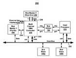
- embedded controller system 200includes a microprocessor 210 that shares the host bus 220 with a multi-channel multi-modal direct memory access (DMA) controller 230 and two slave devices 140 a - 140 b (e.g., random access memory “RAM” units or read-only memory “ROM” units).
- Multi-channel multi-modal DMA controller 230is coupled to the host bus 220 via a front-end interface 232 .
- Embedded controller system 200also includes a bus arbiter 150 , a “fly-by” bus mastering device 240 and a “flow-through” bus mastering device 250 .
- DMA controller 230may also include a back-end interface 238 for interfacing to an external device.
- “fly-by” bus mastering device 240is coupled to the host bus 220 directly for communicating data. Control signals of the “fly-by” bus mastering device 240 , however, are not communicated directly to the host bus 220 . Rather, control signals of the “fly-by” bus mastering device 240 are communicated to a back-end interface 234 interface of DMA controller 230 . “Flow-through” bus mastering device 250 is coupled to the host bus 220 indirectly via the DMA controller 230 through another back-end interface 236 .
- DMA controller 230is a bus mastering device that supports the following modes of operation: (1) fly-by; (2) flow-through; and (3) dual-cycle mode.
- FIG. 3is a timing diagram 300 illustrating an exemplary fly-by mode of operation of the embedded controller system 200 .
- the “fly-by” bus mastering device 240programs the start address and terminal count in the registers (not shown) of the DMA controller 230 , and asserts a DREQI signal 310 .
- DMA controller 230then acknowledges the request by asserting a DACK 1 signal 320 , and also asserts the BRQ 1 signal 340 to the bus arbiter 150 .
- the DMA controller 230acquires the host bus 220 (BGT 1 signal 350 is asserted by bus arbiter 150 ), the DMA controller 230 asserts valid device control signals 234 . As soon as the “fly-by” bus mastering device 240 receives the valid device control signals 234 , it may start driving the data (write cycle) or sampling the data (read cycle) directly on the host bus 220 .
- a memory write operationis performed. That is, as soon as the BGT 1 signal 350 is asserted, DMA controller 230 establishes a DMA channel directly between the “fly-by” bus mastering device 240 and the memory by communicating a DREAD 1 signal 330 to the “fly-by” bus mastering device 240 , and by communicating bus control signals 360 (“ControlA”) and address signals 370 (“AddressA”) to the host bus 220 . Then, data signals 380 (“DataA”) are communicated from the bus mastering device 240 to the host bus 220 .
- fly-by mode of operationthe bus mastering device 240 still acts as a load on the host bus 220 , the loading effect is only on less critical signals, namely the data bus. All other controls are handled by the DMA controller 230 . Because of the latency-intolerance of such devices, no wait states are inserted on the bus 220 . Hence, most of the signals are driven combinatorially from the host bus 220 . Further, according to one embodiment of the present invention, the fly-by mode of operation is recommended only for devices that have significant performance requirement, since the fly-by mode of operation causes an added load on the data bus.
- FIG. 4is a timing diagram 400 illustrating an exemplary flow-through mode of operation of the embedded system 200 in accordance with the present invention.
- “flow-through” bus mastering device 250asserts a signal DREQ 2 410 to the DMA controller 230 .
- DMA controller 230asserts a DACK 2 signal 420 to acknowledge the request, and asserts a DREAD 2 signal 430 to transfer the data (via data signals 440 “DDATA”) from the device 250 into the DMA controller 230 to be stored within its FIFOs (not shown).
- the DMA controller 230then asserts a BRQ 2 450 signal to request control of the host bus 220 .
- the DMA controller 230communicates bus control signals 470 (“ControlB”) and address signals 480 (“AddressB”) to the host bus 220 .
- data signals 490 (“DataB”)are communicated from the DMA controller 230 to the host bus 220 .
- the host bus 220is idling, and if the DMA controller 230 and bus mastering device 250 are synchronous, the latency involved is only 1 clock cycle.
- a FIFO threshold of oneis implemented.
- the exemplary implementation as shown in FIG. 4also attempts to reduce the flow-thru latency by anticipating the availability of the data from the device, and by requesting the host system bus simultaneously with acknowledging the device.
- USBUniversal Serial Bus
- Such devicescan be off loaded from the host bus by using the dual cycle mode of the present invention. Such devices do not need to be a bus master on the host bus. Instead, the devices can reside on a non-bus mastering peripheral-only bus (other than the host bus) that is accessible by the host processor.
- FIG. 5is a timing diagram 500 illustrating an exemplary dual-cycle operation mode for embedded system 200 in accordance with the present invention.
- the host processor 210establishes a DMA channel by programming a start address and a terminal count in the registers of the DMA controller 230 .
- the devicerequests a transfer by asserting DREQ 510 .
- the DMA controller 230then acknowledges the request by asserting DACK 520 , and requests control of the host bus 220 by asserting the BRQ signal 530 .
- the DMA controller 230When the request is granted (bus arbiter 150 asserting the BGT signal 540 ), the DMA controller 230 reads data 570 from the non-bus mastering device by communicating appropriate control signals 550 (“Control”) and address signals 560 (“Address”) to the host bus 230 . The DMA controller then writes the data 570 to the memory by communicating appropriate control signals 550 and address signals 560 to the host bus 220 . After the data is transferred, DMA controller 230 de-asserts DACK 520 indicating that the transfer is complete. The DMA controller 230 may also read data from the memory and transfer it to the non-bus mastering device using the same mechanisms.
- the DMA controllersupports a parametrizable number of channels, each of the channels providing support for either/or mode of operation.
- the DMA controller of the present embodimentserves as bus master on the host bus and has the ability to interface with all the devices on the system.
- the DMA controllermay also be optimized for zero wait state sequential transfers on the host bus.
- the DMA controllermay also house an internal arbiter with programmable priority to choose arbitrate between the different channels, should more than one master that interface to the DMA controller request access to the host bus.
- the DMA controllerhas address-generation logic which provides access to the entire addressable range of the host bus. What is necessary from the bus mastering device point of view is the ability to access the address registers, the terminal count registers and the data registers of the DMA controller. For example, for a 32-bit data bus and an internal FIFO that is 10-word deep, only 4 address pins will suffice to address any location in the 4 GB space. Device firmware would then be responsible for writing the appropriate host address range into the address and count registers. This technique can be particularly useful when the bus mastering interface is an external interface, such as external interface 238 of FIG. 2 .
- Yet another advantage of the present inventionis lower power consumption. If all the bus mastering devices are on the host bus itself, most protocols that support bus mastering require that the bus masters monitor the bus. For example, if there are no bus agents requesting the bus, the arbiter can park the bus on a default bus master. In such cases, the “parked” master will have to drive the bus. But this may fail if the bus mastering devices are shutdown in order to save power, or some other means have to be implemented to “wake up” the bus master before being parked.
- any device connected to a channelcan be turned off at any time of operation, without having to worry about being parked on the host bus.
- the DMA controllerwill drive the necessary signals when the bus is parked on the DMA controller. Additionally, off-loading most bus mastering devices from the host bus can result in a significant power savings due to reduced capacitive loading on the host bus.
- the present inventiona multi-channel multi-modal DMA controller for optimizing the performance of a host bus, has thus been disclosed.
- the present inventiondecreases the loading on the host bus, and thus the host bus can be run at much higher speeds. As a result, a significant increase in throughput can be achieved. Additionally, using shared buses on the DMA side and addressing only the DMA registers reduces the number of I/Os required in the chip. Significant cost savings can also be achieved when the number if I/Os required is reduced. Furthermore, reducing the number of loads on the host bus makes timing analysis and layout much easier. It should be appreciated that, while the present invention has been described in particular embodiments, the present invention should not be construed as limited by such embodiments, but rather construed according to the below
Landscapes
- Engineering & Computer Science (AREA)
- Theoretical Computer Science (AREA)
- Physics & Mathematics (AREA)
- General Engineering & Computer Science (AREA)
- General Physics & Mathematics (AREA)
- Bus Control (AREA)
Abstract
Description
Claims (15)
Priority Applications (5)
| Application Number | Priority Date | Filing Date | Title |
|---|---|---|---|
| US09/593,448US6658502B1 (en) | 2000-06-13 | 2000-06-13 | Multi-channel and multi-modal direct memory access controller for optimizing performance of host bus |
| JP2002511182AJP2004503871A (en) | 2000-06-13 | 2001-06-11 | Direct memory access controller and method |
| PCT/US2001/018761WO2001097046A2 (en) | 2000-06-13 | 2001-06-11 | Multi-mode direct memory access controller and method |
| DE60120700TDE60120700T2 (en) | 2000-06-13 | 2001-06-11 | MULTIMODE DIRECT MEMORY ACCESS CONTROL AND METHOD |
| EP01944419AEP1295210B1 (en) | 2000-06-13 | 2001-06-11 | Multi-mode direct memory access controller and method |
Applications Claiming Priority (1)
| Application Number | Priority Date | Filing Date | Title |
|---|---|---|---|
| US09/593,448US6658502B1 (en) | 2000-06-13 | 2000-06-13 | Multi-channel and multi-modal direct memory access controller for optimizing performance of host bus |
Publications (1)
| Publication Number | Publication Date |
|---|---|
| US6658502B1true US6658502B1 (en) | 2003-12-02 |
Family
ID=24374749
Family Applications (1)
| Application Number | Title | Priority Date | Filing Date |
|---|---|---|---|
| US09/593,448Expired - LifetimeUS6658502B1 (en) | 2000-06-13 | 2000-06-13 | Multi-channel and multi-modal direct memory access controller for optimizing performance of host bus |
Country Status (5)
| Country | Link |
|---|---|
| US (1) | US6658502B1 (en) |
| EP (1) | EP1295210B1 (en) |
| JP (1) | JP2004503871A (en) |
| DE (1) | DE60120700T2 (en) |
| WO (1) | WO2001097046A2 (en) |
Cited By (5)
| Publication number | Priority date | Publication date | Assignee | Title |
|---|---|---|---|---|
| US20060031603A1 (en)* | 2004-08-09 | 2006-02-09 | Bradfield Travis A | Multi-threaded/multi-issue DMA engine data transfer system |
| US7107374B1 (en)* | 2001-09-05 | 2006-09-12 | Xilinx, Inc. | Method for bus mastering for devices resident in configurable system logic |
| US20070174507A1 (en)* | 2005-12-23 | 2007-07-26 | Conti Gregory R | Methods and Systems to Restrict Usage of a DMA Channel |
| US7478186B1 (en)* | 2004-06-03 | 2009-01-13 | Integrated Device Technology, Inc. | Interrupt coalescer for DMA channel |
| CN114297105A (en)* | 2021-12-29 | 2022-04-08 | 合肥市芯海电子科技有限公司 | Embedded control circuit, chip and electronic equipment for direct memory access |
Families Citing this family (1)
| Publication number | Priority date | Publication date | Assignee | Title |
|---|---|---|---|---|
| DE102011088020A1 (en)* | 2011-12-08 | 2013-06-13 | Bayerische Motoren Werke Aktiengesellschaft | Communication device for a motor vehicle |
Citations (11)
| Publication number | Priority date | Publication date | Assignee | Title |
|---|---|---|---|---|
| US4523310A (en)* | 1983-01-28 | 1985-06-11 | Gould Computer Systems Inc. | Synchronous communications multiplexer |
| US5416916A (en) | 1990-07-06 | 1995-05-16 | Nec Electronics Incorporated | Structure for enabling direct memory-to-memory transfer with a fly-by DMA unit |
| EP0775960A2 (en) | 1995-11-21 | 1997-05-28 | International Business Machines Corporation | Bus interface logic system |
| US5764934A (en)* | 1996-07-03 | 1998-06-09 | Intel Corporation | Processor subsystem for use with a universal computer architecture |
| US5805927A (en) | 1994-01-28 | 1998-09-08 | Apple Computer, Inc. | Direct memory access channel architecture and method for reception of network information |
| US5845107A (en)* | 1996-07-03 | 1998-12-01 | Intel Corporation | Signaling protocol conversion between a processor and a high-performance system bus |
| US5896513A (en)* | 1996-07-03 | 1999-04-20 | Intel Corporation | Computer system providing a universal architecture adaptive to a variety of processor types and bus protocols |
| US6055584A (en) | 1997-11-20 | 2000-04-25 | International Business Machines Corporation | Processor local bus posted DMA FlyBy burst transfers |
| US6202106B1 (en)* | 1998-09-09 | 2001-03-13 | Xilinx, Inc. | Method for providing specific knowledge of a structure of parameter blocks to an intelligent direct memory access controller |
| US6219724B1 (en)* | 1997-11-29 | 2001-04-17 | Electronics And Telecommunications Research Institute | Direct memory access controller |
| US6289023B1 (en)* | 1997-09-25 | 2001-09-11 | Hewlett-Packard Company | Hardware checksum assist for network protocol stacks |
- 2000
- 2000-06-13USUS09/593,448patent/US6658502B1/ennot_activeExpired - Lifetime
- 2001
- 2001-06-11WOPCT/US2001/018761patent/WO2001097046A2/enactiveIP Right Grant
- 2001-06-11EPEP01944419Apatent/EP1295210B1/ennot_activeExpired - Lifetime
- 2001-06-11DEDE60120700Tpatent/DE60120700T2/ennot_activeExpired - Lifetime
- 2001-06-11JPJP2002511182Apatent/JP2004503871A/ennot_activeWithdrawn
Patent Citations (11)
| Publication number | Priority date | Publication date | Assignee | Title |
|---|---|---|---|---|
| US4523310A (en)* | 1983-01-28 | 1985-06-11 | Gould Computer Systems Inc. | Synchronous communications multiplexer |
| US5416916A (en) | 1990-07-06 | 1995-05-16 | Nec Electronics Incorporated | Structure for enabling direct memory-to-memory transfer with a fly-by DMA unit |
| US5805927A (en) | 1994-01-28 | 1998-09-08 | Apple Computer, Inc. | Direct memory access channel architecture and method for reception of network information |
| EP0775960A2 (en) | 1995-11-21 | 1997-05-28 | International Business Machines Corporation | Bus interface logic system |
| US5764934A (en)* | 1996-07-03 | 1998-06-09 | Intel Corporation | Processor subsystem for use with a universal computer architecture |
| US5845107A (en)* | 1996-07-03 | 1998-12-01 | Intel Corporation | Signaling protocol conversion between a processor and a high-performance system bus |
| US5896513A (en)* | 1996-07-03 | 1999-04-20 | Intel Corporation | Computer system providing a universal architecture adaptive to a variety of processor types and bus protocols |
| US6289023B1 (en)* | 1997-09-25 | 2001-09-11 | Hewlett-Packard Company | Hardware checksum assist for network protocol stacks |
| US6055584A (en) | 1997-11-20 | 2000-04-25 | International Business Machines Corporation | Processor local bus posted DMA FlyBy burst transfers |
| US6219724B1 (en)* | 1997-11-29 | 2001-04-17 | Electronics And Telecommunications Research Institute | Direct memory access controller |
| US6202106B1 (en)* | 1998-09-09 | 2001-03-13 | Xilinx, Inc. | Method for providing specific knowledge of a structure of parameter blocks to an intelligent direct memory access controller |
Cited By (10)
| Publication number | Priority date | Publication date | Assignee | Title |
|---|---|---|---|---|
| US7107374B1 (en)* | 2001-09-05 | 2006-09-12 | Xilinx, Inc. | Method for bus mastering for devices resident in configurable system logic |
| US7478186B1 (en)* | 2004-06-03 | 2009-01-13 | Integrated Device Technology, Inc. | Interrupt coalescer for DMA channel |
| US20060031603A1 (en)* | 2004-08-09 | 2006-02-09 | Bradfield Travis A | Multi-threaded/multi-issue DMA engine data transfer system |
| US20070174507A1 (en)* | 2005-12-23 | 2007-07-26 | Conti Gregory R | Methods and Systems to Restrict Usage of a DMA Channel |
| WO2007076340A3 (en)* | 2005-12-23 | 2008-04-24 | Texas Instruments Inc | Methods and systems to restrict usage of a dma channel |
| US9740887B2 (en) | 2005-12-23 | 2017-08-22 | Texas Instruments Incorporated | Methods and systems to restrict usage of a DMA channel |
| US12141333B2 (en) | 2005-12-23 | 2024-11-12 | Texas Instruments Incorporated | Methods and systems to restrict usage of a DMA channel |
| US12346488B2 (en) | 2005-12-23 | 2025-07-01 | Texas Instruments Incorporated | Methods and systems to restrict usage of a DMA channel |
| CN114297105A (en)* | 2021-12-29 | 2022-04-08 | 合肥市芯海电子科技有限公司 | Embedded control circuit, chip and electronic equipment for direct memory access |
| CN114297105B (en)* | 2021-12-29 | 2024-04-05 | 合肥市芯海电子科技有限公司 | Embedded control circuit, chip and electronic equipment for direct memory access |
Also Published As
| Publication number | Publication date |
|---|---|
| JP2004503871A (en) | 2004-02-05 |
| DE60120700D1 (en) | 2006-07-27 |
| EP1295210A2 (en) | 2003-03-26 |
| WO2001097046A2 (en) | 2001-12-20 |
| WO2001097046A3 (en) | 2002-04-04 |
| EP1295210B1 (en) | 2006-06-14 |
| DE60120700T2 (en) | 2007-05-31 |
Similar Documents
| Publication | Publication Date | Title |
|---|---|---|
| AU651747B2 (en) | Arbitration control logic for computer system having dual bus architecture | |
| US4991085A (en) | Personal computer bus interface chip with multi-function address relocation pins | |
| US4937734A (en) | High speed bus with virtual memory data transfer and rerun cycle capability | |
| JP4500373B2 (en) | Computer system with integrated system memory and improved bus concurrency | |
| EP1038231B1 (en) | Mechanism that performs interrupt destination redirection | |
| US6040845A (en) | Device and method for reducing power consumption within an accelerated graphics port target | |
| US5659696A (en) | Method and apparatus for determining address location and taking one of two actions depending on the type of read/write data transfer required | |
| US5121487A (en) | High speed bus with virtual memory data transfer capability using virtual address/data lines | |
| US6199134B1 (en) | Computer system with bridge logic that asserts a system management interrupt signal when an address is made to a trapped address and which also completes the cycle to the target address | |
| US8180947B2 (en) | USB on-the-go controller | |
| EP0628914A1 (en) | System direct memory access (DMA) support logic for PCI based computer system | |
| US5761454A (en) | Deadlock resolution methods and apparatus for interfacing concurrent and asynchronous buses | |
| US20080133787A1 (en) | Method and apparatus for host messaging unit for peripheral component interconnect busmaster devices | |
| US6079024A (en) | Bus interface unit having selectively enabled buffers | |
| WO2001097006A1 (en) | Memory controller hub | |
| US6658502B1 (en) | Multi-channel and multi-modal direct memory access controller for optimizing performance of host bus | |
| US6519670B1 (en) | Method and system for optimizing a host bus that directly interfaces to a 16-bit PCMCIA host bus adapter | |
| US5933613A (en) | Computer system and inter-bus control circuit | |
| US7327370B2 (en) | Memory controller hub interface | |
| US20070124610A1 (en) | Power management device for multiprocessor system and method thereof | |
| US5097483A (en) | Tri-statable bus with apparatus to drive bus line to first level and then second level for predetermined time before turning off | |
| US20030236941A1 (en) | Data processor | |
| US20060206644A1 (en) | Method of hot switching data transfer rate on bus | |
| JP3402049B2 (en) | Information processing apparatus and information processing apparatus control method | |
| JP2001265714A (en) | Interface device and information processing system provided with the same |
Legal Events
| Date | Code | Title | Description |
|---|---|---|---|
| AS | Assignment | Owner name:PHILIPS ELECTRONICS NORTH AMERICAN CORPORATION, NE Free format text:ASSIGNMENT OF ASSIGNORS INTEREST;ASSIGNOR:MEIYAPPAN, SUBRAMANIAN S.;REEL/FRAME:011184/0627 Effective date:20001009 Owner name:PHILIPS ELECTRONICS NORTH AMERICAN CORPORATION, NE Free format text:ASSIGNMENT OF ASSIGNORS INTEREST;ASSIGNOR:STORY, FRANKLYN H.;REEL/FRAME:011184/0641 Effective date:20000606 | |
| AS | Assignment | Owner name:KONINKLIJKE PHILIPS ELECTRONICS N.V., NETHERLANDS Free format text:ASSIGNMENT OF ASSIGNORS INTEREST;ASSIGNOR:PHILIPS ELECTRONICS NORTH AMERICA CORP.;REEL/FRAME:014573/0536 Effective date:20031006 | |
| STCF | Information on status: patent grant | Free format text:PATENTED CASE | |
| AS | Assignment | Owner name:NXP B.V., NETHERLANDS Free format text:ASSIGNMENT OF ASSIGNORS INTEREST;ASSIGNOR:PHILIPS ELECTRONICS NORTH AMERICA CORP.;REEL/FRAME:018654/0521 Effective date:20061213 | |
| FPAY | Fee payment | Year of fee payment:4 | |
| AS | Assignment | Owner name:NXP B.V., NETHERLANDS Free format text:ASSIGNMENT OF ASSIGNORS INTEREST;ASSIGNOR:KONINKLIJKE PHILIPS ELECTRONICS N.V.;REEL/FRAME:023649/0989 Effective date:20091215 | |
| FPAY | Fee payment | Year of fee payment:8 | |
| AS | Assignment | Owner name:PARTNERS FOR CORPORATE RESEARCH INTERNATIONAL, CAY Free format text:ASSIGNMENT OF ASSIGNORS INTEREST;ASSIGNOR:NXP B. V.;REEL/FRAME:031334/0449 Effective date:20120907 | |
| AS | Assignment | Owner name:FUTURE LINK SYSTEMS, CALIFORNIA Free format text:ASSIGNMENT OF ASSIGNORS INTEREST;ASSIGNOR:PARTNERS FOR CORPORATE RESEARCH INTERNATIONAL;REEL/FRAME:032399/0965 Effective date:20130808 | |
| FPAY | Fee payment | Year of fee payment:12 |