US6658041B2 - Wafer bonded vertical cavity surface emitting laser systems - Google Patents
Wafer bonded vertical cavity surface emitting laser systemsDownload PDFInfo
- Publication number
- US6658041B2 US6658041B2US10/102,294US10229402AUS6658041B2US 6658041 B2US6658041 B2US 6658041B2US 10229402 AUS10229402 AUS 10229402AUS 6658041 B2US6658041 B2US 6658041B2
- Authority
- US
- United States
- Prior art keywords
- mirror
- optically transparent
- region
- stack structure
- transparent substrate
- Prior art date
- Legal status (The legal status is an assumption and is not a legal conclusion. Google has not performed a legal analysis and makes no representation as to the accuracy of the status listed.)
- Expired - Lifetime
Links
Images


Classifications
- H—ELECTRICITY
- H01—ELECTRIC ELEMENTS
- H01S—DEVICES USING THE PROCESS OF LIGHT AMPLIFICATION BY STIMULATED EMISSION OF RADIATION [LASER] TO AMPLIFY OR GENERATE LIGHT; DEVICES USING STIMULATED EMISSION OF ELECTROMAGNETIC RADIATION IN WAVE RANGES OTHER THAN OPTICAL
- H01S5/00—Semiconductor lasers
- H01S5/10—Construction or shape of the optical resonator, e.g. extended or external cavity, coupled cavities, bent-guide, varying width, thickness or composition of the active region
- H01S5/18—Surface-emitting [SE] lasers, e.g. having both horizontal and vertical cavities
- H01S5/183—Surface-emitting [SE] lasers, e.g. having both horizontal and vertical cavities having only vertical cavities, e.g. vertical cavity surface-emitting lasers [VCSEL]
- H01S5/18386—Details of the emission surface for influencing the near- or far-field, e.g. a grating on the surface
- H01S5/18388—Lenses
- H—ELECTRICITY
- H01—ELECTRIC ELEMENTS
- H01S—DEVICES USING THE PROCESS OF LIGHT AMPLIFICATION BY STIMULATED EMISSION OF RADIATION [LASER] TO AMPLIFY OR GENERATE LIGHT; DEVICES USING STIMULATED EMISSION OF ELECTROMAGNETIC RADIATION IN WAVE RANGES OTHER THAN OPTICAL
- H01S5/00—Semiconductor lasers
- H01S5/02—Structural details or components not essential to laser action
- H01S5/0206—Substrates, e.g. growth, shape, material, removal or bonding
- H01S5/0215—Bonding to the substrate
- H—ELECTRICITY
- H01—ELECTRIC ELEMENTS
- H01S—DEVICES USING THE PROCESS OF LIGHT AMPLIFICATION BY STIMULATED EMISSION OF RADIATION [LASER] TO AMPLIFY OR GENERATE LIGHT; DEVICES USING STIMULATED EMISSION OF ELECTROMAGNETIC RADIATION IN WAVE RANGES OTHER THAN OPTICAL
- H01S5/00—Semiconductor lasers
- H01S5/02—Structural details or components not essential to laser action
- H01S5/022—Mountings; Housings
- H01S5/0225—Out-coupling of light
- H01S5/02251—Out-coupling of light using optical fibres
- H—ELECTRICITY
- H01—ELECTRIC ELEMENTS
- H01S—DEVICES USING THE PROCESS OF LIGHT AMPLIFICATION BY STIMULATED EMISSION OF RADIATION [LASER] TO AMPLIFY OR GENERATE LIGHT; DEVICES USING STIMULATED EMISSION OF ELECTROMAGNETIC RADIATION IN WAVE RANGES OTHER THAN OPTICAL
- H01S5/00—Semiconductor lasers
- H01S5/02—Structural details or components not essential to laser action
- H01S5/022—Mountings; Housings
- H01S5/0233—Mounting configuration of laser chips
- H01S5/0234—Up-side down mountings, e.g. Flip-chip, epi-side down mountings or junction down mountings
- H—ELECTRICITY
- H01—ELECTRIC ELEMENTS
- H01S—DEVICES USING THE PROCESS OF LIGHT AMPLIFICATION BY STIMULATED EMISSION OF RADIATION [LASER] TO AMPLIFY OR GENERATE LIGHT; DEVICES USING STIMULATED EMISSION OF ELECTROMAGNETIC RADIATION IN WAVE RANGES OTHER THAN OPTICAL
- H01S5/00—Semiconductor lasers
- H01S5/02—Structural details or components not essential to laser action
- H01S5/022—Mountings; Housings
- H01S5/0235—Method for mounting laser chips
- H01S5/02355—Fixing laser chips on mounts
- H01S5/0237—Fixing laser chips on mounts by soldering
- H—ELECTRICITY
- H01—ELECTRIC ELEMENTS
- H01S—DEVICES USING THE PROCESS OF LIGHT AMPLIFICATION BY STIMULATED EMISSION OF RADIATION [LASER] TO AMPLIFY OR GENERATE LIGHT; DEVICES USING STIMULATED EMISSION OF ELECTROMAGNETIC RADIATION IN WAVE RANGES OTHER THAN OPTICAL
- H01S5/00—Semiconductor lasers
- H01S5/10—Construction or shape of the optical resonator, e.g. extended or external cavity, coupled cavities, bent-guide, varying width, thickness or composition of the active region
- H01S5/18—Surface-emitting [SE] lasers, e.g. having both horizontal and vertical cavities
- H01S5/183—Surface-emitting [SE] lasers, e.g. having both horizontal and vertical cavities having only vertical cavities, e.g. vertical cavity surface-emitting lasers [VCSEL]
- H01S5/18305—Surface-emitting [SE] lasers, e.g. having both horizontal and vertical cavities having only vertical cavities, e.g. vertical cavity surface-emitting lasers [VCSEL] with emission through the substrate, i.e. bottom emission
- H—ELECTRICITY
- H01—ELECTRIC ELEMENTS
- H01S—DEVICES USING THE PROCESS OF LIGHT AMPLIFICATION BY STIMULATED EMISSION OF RADIATION [LASER] TO AMPLIFY OR GENERATE LIGHT; DEVICES USING STIMULATED EMISSION OF ELECTROMAGNETIC RADIATION IN WAVE RANGES OTHER THAN OPTICAL
- H01S5/00—Semiconductor lasers
- H01S5/10—Construction or shape of the optical resonator, e.g. extended or external cavity, coupled cavities, bent-guide, varying width, thickness or composition of the active region
- H01S5/18—Surface-emitting [SE] lasers, e.g. having both horizontal and vertical cavities
- H01S5/183—Surface-emitting [SE] lasers, e.g. having both horizontal and vertical cavities having only vertical cavities, e.g. vertical cavity surface-emitting lasers [VCSEL]
- H01S5/18308—Surface-emitting [SE] lasers, e.g. having both horizontal and vertical cavities having only vertical cavities, e.g. vertical cavity surface-emitting lasers [VCSEL] having a special structure for lateral current or light confinement
- H01S5/18311—Surface-emitting [SE] lasers, e.g. having both horizontal and vertical cavities having only vertical cavities, e.g. vertical cavity surface-emitting lasers [VCSEL] having a special structure for lateral current or light confinement using selective oxidation
- H01S5/18313—Surface-emitting [SE] lasers, e.g. having both horizontal and vertical cavities having only vertical cavities, e.g. vertical cavity surface-emitting lasers [VCSEL] having a special structure for lateral current or light confinement using selective oxidation by oxidizing at least one of the DBR layers
- H—ELECTRICITY
- H01—ELECTRIC ELEMENTS
- H01S—DEVICES USING THE PROCESS OF LIGHT AMPLIFICATION BY STIMULATED EMISSION OF RADIATION [LASER] TO AMPLIFY OR GENERATE LIGHT; DEVICES USING STIMULATED EMISSION OF ELECTROMAGNETIC RADIATION IN WAVE RANGES OTHER THAN OPTICAL
- H01S5/00—Semiconductor lasers
- H01S5/10—Construction or shape of the optical resonator, e.g. extended or external cavity, coupled cavities, bent-guide, varying width, thickness or composition of the active region
- H01S5/18—Surface-emitting [SE] lasers, e.g. having both horizontal and vertical cavities
- H01S5/183—Surface-emitting [SE] lasers, e.g. having both horizontal and vertical cavities having only vertical cavities, e.g. vertical cavity surface-emitting lasers [VCSEL]
- H01S5/18308—Surface-emitting [SE] lasers, e.g. having both horizontal and vertical cavities having only vertical cavities, e.g. vertical cavity surface-emitting lasers [VCSEL] having a special structure for lateral current or light confinement
- H01S5/18322—Position of the structure
- H01S5/1833—Position of the structure with more than one structure
- H01S5/18333—Position of the structure with more than one structure only above the active layer
Definitions
- This inventionrelates to wafer bonded vertical cavity surface emitting laser (VCSEL) systems and methods of making the same.
- VCSELvertical cavity surface emitting laser
- a VCSELis a laser device formed from an optically active semiconductor layer (e.g., AlInGaAs or InGaAsP) that is sandwiched between a pair of highly reflective mirror stacks, which may be formed from layers of metallic material, dielectric material or epitaxially-grown semiconductor material.
- an optically active semiconductor layere.g., AlInGaAs or InGaAsP
- one of the mirror stacksis made less reflective than the other so that a portion of the coherent light that builds in a resonating cavity formed in the optically active semiconductor layer between the mirror stacks may be emitted from the device.
- a VCSELemits laser light from the top or bottom surface of the resonating cavity with a relatively small beam divergence.
- VCSELsmay be arranged in singlets, one-dimensional or two-dimensional arrays, tested on wafer, and incorporated easily into an optical transceiver module that may be coupled to a fiber optic cable.
- a wafer bonding techniquemay be characterized as a direct wafer bonding technique or a metallic wafer bonding technique.
- direct wafer bondingtwo wafers are fused together by mass transport at a bonding interface.
- Direct wafer bondingmay be performed between any combination of semiconductor, oxide, and dielectric materials.
- Direct wafer bondingtypically is performed at high temperature and under uniaxial pressure.
- metallic wafer bondingtwo substrates are bonded together by a metallic layer that is melted and re-solidified at a bonding interface.
- Wafer bonding techniqueshave been used in the fabrication of optoelectronic devices.
- U.S. Pat. No. 6,320,206has proposed a scheme for forming optical devices having aluminum gallium indium nitride active layers and high quality mirror stacks that are wafer bonded on one or both sides of the active layers.
- U.S. Pat. No. 5,837,561describes a vertical cavity surface emitting laser that is wafer bonded to a transparent substrate.
- a top circular metal contactis disposed on the transparent substrate and a second metal contact is disposed over the bottom mirror of the vertical cavity surface emitting laser.
- the transparent substrateserves as an escape medium for laser emission through the top circular metal contact. This configuration allows the heat producing active layer of the vertical cavity surface emitting laser to be mounted near a heat sink, thereby improving the performance of the device.
- the inventionfeatures vertical cavity surface emitting laser systems and methods of making the same.
- the inventionfeatures a vertical cavity surface emitting laser system having a bottom side that may be flip-chip mounted to a driver substrate and a top side configured to transmit light through an optically transparent substrate.
- the inventionenables vertical cavity surface emitting laser systems to be packed together with a greater density and operated at greater speeds relative to, for example, wire bonded vertical cavity surface emitting laser systems.
- such systemsmay be flexibly tailored to produce light over a wide range of wavelengths.
- Such systemsalso may be efficiently packaged on a wafer scale.
- the inventionfeatures a vertical cavity surface emitting laser (VCSEL) system, comprising a substrate, a vertical stack structure, and a pair of contacts.
- the substrateis optically transparent to light in a selected wavelength range.
- the vertical stack structurehas a substantially planar top side, which is wafer bonded to the optically transparent substrate, and a bottom side.
- the vertical stack structureincludes a top mirror, a bottom mirror, and a cavity region that is disposed between the top mirror and the bottom mirror and includes an active light generation region that is operable to generate light in the selected wavelength range.
- the vertical stack structureis constructed and arranged to direct light generated in the cavity region to the optically transparent substrate.
- First and second contactsare disposed over the bottom side of the vertical stack structure and are electrically connected for driving the cavity region.
- Embodiments in accordance with this aspect of the inventionmay include one or more of the following features.
- the optically transparent substratecomprises glass (e.g., borosilicate glass). In other embodiments, the optically transparent substrate comprises gallium phosphide.
- the VCSEL systemmay further comprise a lens that is disposed on the glass substrate in alignment with the active light generation region.
- the top mirror and the bottom mirrorhas a layer with a peripheral region that is oxidized into an electrical insulator as a result of exposure to an oxidizing agent.
- the VCSEL systemmay further comprise two or more etched holes each extending from a substantially planar surface of the bottom mirror to the oxidized peripheral region.
- the top mirror and the bottom mirrorpreferably each comprises a system of alternating layers of different refractive index materials.
- the top mirror and the bottom mirroreach may comprise a system of alternating layers of relatively high aluminum content AlGaAs and relatively low aluminum content AlGaAs.
- the VCSEL systemfurther comprises an integrated circuit that is bonded to the pair of contacts and is operable to drive the cavity region.
- the inventionfeatures a method of fabricating the above described VCSEL system.
- a sacrificial substrateis provided.
- a vertical stack structure having a substantially planar top side and a bottom sideis formed over the vertical stack structure.
- the vertical stack structureincludes a top mirror, a bottom mirror, and a cavity region that is disposed between the top mirror and the bottom mirror and includes an active light generation region operable to generate light in a selected wavelength range.
- the vertical stack structureis constructed and arranged to direct light generated in the cavity region away from the sacrificial substrate.
- the substantially planar top side of the vertical stack structureis wafer bonded to a substrate that is optically transparent to light in the selected wavelength range.
- the sacrificial substrateis removed after the optically transparent substrate has been wafer bonded to the substantially planar top side of the vertical stack structure.
- First and second contacts that are electrically connected for driving the cavity regionare formed over the bottom side of the vertical stack structure.
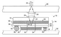
- FIG. 1is a diagrammatic cross-sectional side view of a vertical cavity surface emitting laser system that is flip chip mounted to a driver substrate and an optical fiber positioned on an opposite side of a package window to receive light generated by the vertical cavity surface emitting laser system.
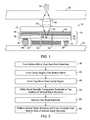
- FIG. 2is a flow diagram of a method of making the vertical cavity surface emitting laser system of FIG. 1 .
- FIG. 3Ais a diagrammatic cross-sectional side view of a bottom mirror formed over a sacrificial substrate.
- FIG. 3Bis a diagrammatic cross-sectional side view of a cavity region formed over the bottom mirror of FIG. 3 A.
- FIG. 3Cis a diagrammatic cross-sectional side view of a top mirror formed over the cavity region of FIG. 3 B and oxidation holes formed in the resulting vertical stack structure.
- FIG. 3Dis a diagrammatic cross-sectional side view of an optically transparent substrate wafer bonded to the top mirror of FIG. 3 C.
- FIG. 3Eis a diagrammatic cross-sectional side view of the vertical cavity surface emitting laser system of FIG. 3D after the sacrificial substrate has been removed.
- FIG. 3Fis a diagrammatic cross-sectional side view of the vertical cavity surface emitting laser system of FIG. 3E after the bottom surface has been patterned and a pair of contacts has been formed over a bottom side of the vertical stack structure.
- a vertical cavity surface emitting laser system 10includes an optically transparent substrate 12 , a vertical stack structure 14 , and a pair of contacts 16 , 18 that are flip chip bonded to a driver substrate 20 .
- a driving circuit disposed on driver substrate 20applies a current between contacts 16 , 18 that drives vertical stack structure 14 to generate light 22 in a selected wavelength range.
- Light 22passes through optically transparent substrate 12 and is collimated by a first lens 24 that is disposed on optically transparent substrate 12 .
- a second lens 26which is disposed on an optically transparent package window 28 , focuses the collimated light 22 received from first lens 24 into an optical fiber 30 .
- vertical cavity surface emitting laser system 10may be fabricated as follows.
- Bottom mirror stack 32is formed on a sacrificial substrate 34 (step 36 ; FIG. 2 ).
- Bottom mirror stack 32includes a system of alternating layers of different refractive index materials that forms a distributed Bragg reflector (DBR) that is designed for a desired operating laser wavelength (e.g., a wavelength in the range of 650 nm to 1650 nm).
- DBRdistributed Bragg reflector
- bottom mirror stack 32may be formed, of alternating layers of high aluminum content AlGaAs and low aluminum content AlGaAs.
- the layers of bottom mirror stack 32preferably have an effective optical thickness (i.e., the layer thickness multiplied by the refractive index of the layer) that is about one-quarter of the operating laser wavelength.
- Sacrificial substrate 34preferably is formed from a material that is lattice-matched to the layers of bottom mirror stack 32 .
- sacrificial substrate 34may be formed from GaAs, InP, sapphire (Al 2 O 3 ), or InGaAs and may be undoped, doped n-type (e.g., with Si) or doped p-type (e.g., with Zn).
- a buffer layer(not shown) may be grown on sacrificial substrate 34 before bottom mirror stack 32 is formed.
- a cavity region 38is formed over bottom mirror stack 32 (step 40 ; FIG. 2 ).
- Cavity region 38includes one or more active layers 42 , 44 (e.g., a quantum well or one or more quantum dots).
- active layers 42 , 44may be sandwiched between a pair of spacer layers (not shown). In other embodiments, active layers 42 , 44 may be located above or below a single spacer layer.
- Active layers 42 , 44may be formed from AlInGaAs (i.e., AlInGaAs, GaAs, AlGaAs and InGaAs), InGaAsP (i.e., InGaAsP, GaAs, InGaAs, GaAsP, and GaP), GaAsSb (i.e., GaAsSb, GaAs, and GaSb), InGaAsN (i.e., InGaAsN, GaAs, InGaAs, GaAsN, and GaN), or AlInGaAsP (i.e., AlInGaAsP, AlInGaAs, AlGaAs, InGaAs, InGaAsP, GaAs, InGaAs, GaAsP, and GaP).
- Other quantum well layer compositionsalso may be used.
- the first and second spacer layersmay be formed from materials chosen based upon the material composition of the active layers.
- a top mirror stack 46is formed over cavity region 38 (step 48 ; FIG. 2 ).
- Top mirror stack 46preferably is formed from the same material system as bottom mirror stack 32 .
- bottom and top mirror stacks 32 , 46are cooperatively designed so that laser light 22 is emitted from a substantially planar top surface 50 of vertical stack structure 14 and through optically transparent substrate 12 (see FIG. 1 ).
- the layers of vertical stack structure 14may be formed by conventional epitaxial growth processes, such as metal-organic chemical vapor deposition (MOCVD) and molecular beam epitaxy (MBE).
- MOCVDmetal-organic chemical vapor deposition
- MBEmolecular beam epitaxy
- vertical stack structure 14has a planar structure that includes a number of holes 52 , 54 that expose a number of respective side regions of the bottom and top mirror stacks 32 , 46 to be oxidized. At least a portion of each of bottom mirror stack 32 and top mirror stack 46 is oxidized from the exposed side regions inwardly toward a centrally located aperture region 56 .
- four holesare opened at locations that are equidistant from the center of aperture region 56 .
- the holes 52 , 54extend from a bottom surface of bottom mirror stack 32 to the layer (or layers) corresponding to the portion of vertical stack structure 14 to be oxidized.
- the heated water vaporenters the holes and oxidizes one or more layers of vertical stack structure 14 in a radial direction away from the holes. The oxidation process continues until an oxidation front from each hole merges to form the un-oxidized aperture region 56 .
- Other vertical stack structure embodimentsmay include more or fewer exposure holes or exposed regions with other shapes, such as divided arcs or rings.
- optically transparent substrate 12is wafer bonded to the substantially planar top surface 50 of vertical stack structure 14 (step 58 ; FIG. 2 ).
- the optically transparent substrate 12preferably is substantially transparent to light in a selected wavelength range.
- the selected wavelength rangeencompasses the wavelength of light generated by vertical stack structure 14 .
- the optically transparent substrate 12is substantially transparent to light having a wavelength in the range of 650 nm to 1650 nm.
- optically transparent substrate 12is formed from glass (e.g., borosilicate glass).
- optically transparent substrate 12is formed from gallium phosphide. In other embodiments, optically transparent substrate 12 may be formed from other materials. In general, optically transparent substrate 12 may be attached to surface 50 by a conventional direct wafer bonding process or a conventional metallic bonding process that is tailored to the selected material systems of optically transparent substrate 12 and vertical stack structure 14 .
- sacrificial substrate 34is removed (step 60 ; FIG. 2 ).
- sacrificial substrate 34may be removed by any one of a wide variety of conventional substrate removal processes.
- sacrificial substrate 34may be removed by a selective wet chemical etching process.
- an etch stop layer 62(see FIG. 3D) preferably is formed between the sacrificial substrate 34 and bottom mirror stack 32 .
- sacrificial substrate 34may be removed by laser melting. In some embodiments, etch stop layer 62 also may be removed.
- vertical stack structureis patterned and etched, and contacts 16 , 18 are formed over the bottom side of the patterned vertical stack structure (step 64 ; FIG. 2 ).
- the vertical stack structuremay be formed by a conventional photolithographic patterning and etching process.
- lens 24is formed on the opposite surface of optically transparent substrate 12 as the vertical stack structure 14 .
- Lens 24(and the corresponding lens 26 of package window 28 ) may be a replicated epoxy lens or a diffractive optical element (DOE).
- DOEdiffractive optical element
- contacts 16 , 18may be bonded to corresponding contacts of a suitable driving circuit disposed on driver substrate 20 using a flip-chip solder bonding process.
- solder bumps 66 , 68are disposed between contacts 16 , 18 and the corresponding metallization pattern of the driving circuit.
- the Z-axis dimensions 4 , of solder bumps 66 , 68are selected to separate the bottom side of vertical stack structure 14 from the driving circuit by an appropriate distance.
- solder bumps 66 , 68originally may be disposed on the metallization pattern of the driving circuit.
- Vertical cavity surface emitting laser system 10is aligned with the driving circuit to within an accuracy required for solder bumps 66 , 68 to contact the corresponding driving circuit metallization pattern.
- the assemblythen is raised to a temperature at or above the melting point of solder bumps 66 , 68 .
- Solder bumps 66 , 68wet the solderable contacts 16 , 18 and surface tension forces pull vertical cavity surface emitting laser system 10 and driver substrate 20 into very precise alignment (e.g., to within ⁇ 4 ⁇ m).
- the assemblyis cooled to form a solidly bonded, accurately aligned structure.
- Electrical contacts 16 , 18enable vertical cavity surface emitting laser system 10 to be driven by the driving circuit that is disposed on driver substrate 20 .
- an operating voltageis applied across electrical contacts 16 , 18 to produce a current flow in vertical stack structure 14 .
- currentflows through a central region of the vertical stack structure 14 and lasing occurs in a central portion of cavity region 38 (hereinafter the “active region”).
- the oxidized portions of bottom and top mirror stacks 32 , 36form an oxide confinement region that laterally confines carriers and photons. Carrier confinement results from the relatively high electrical resistivity of the confinement region, which causes electrical current preferentially to flow through a centrally located region of vertical stack structure 14 .
- Optical confinementresults from a substantial reduction of the refractive index of the confinement region that creates a lateral refractive index profile that guides the photons that are generated in cavity region 38 .
- the carrier and optical lateral confinementincreases the density of carriers and photons within the active region and, consequently, increases the efficiency with which light is generated within the active region.
Landscapes
- Physics & Mathematics (AREA)
- Condensed Matter Physics & Semiconductors (AREA)
- General Physics & Mathematics (AREA)
- Electromagnetism (AREA)
- Optics & Photonics (AREA)
- Semiconductor Lasers (AREA)
Abstract
Description
Claims (22)
Priority Applications (1)
| Application Number | Priority Date | Filing Date | Title |
|---|---|---|---|
| US10/102,294US6658041B2 (en) | 2002-03-20 | 2002-03-20 | Wafer bonded vertical cavity surface emitting laser systems |
Applications Claiming Priority (1)
| Application Number | Priority Date | Filing Date | Title |
|---|---|---|---|
| US10/102,294US6658041B2 (en) | 2002-03-20 | 2002-03-20 | Wafer bonded vertical cavity surface emitting laser systems |
Publications (2)
| Publication Number | Publication Date |
|---|---|
| US20030179800A1 US20030179800A1 (en) | 2003-09-25 |
| US6658041B2true US6658041B2 (en) | 2003-12-02 |
Family
ID=28040177
Family Applications (1)
| Application Number | Title | Priority Date | Filing Date |
|---|---|---|---|
| US10/102,294Expired - LifetimeUS6658041B2 (en) | 2002-03-20 | 2002-03-20 | Wafer bonded vertical cavity surface emitting laser systems |
Country Status (1)
| Country | Link |
|---|---|
| US (1) | US6658041B2 (en) |
Cited By (27)
| Publication number | Priority date | Publication date | Assignee | Title |
|---|---|---|---|---|
| US20040264541A1 (en)* | 2003-06-25 | 2004-12-30 | Honeywell International Inc. | InP based long wavelength VCSEL |
| US20060013276A1 (en)* | 2004-07-15 | 2006-01-19 | Mchugo Scott A | VCSEL having an air gap and protective coating |
| US20060126694A1 (en)* | 2004-12-14 | 2006-06-15 | Kwon O Kyun | Hybrid metal bonded vertical cavity surface emitting laser and fabricating method thereof |
| US20060154393A1 (en)* | 2005-01-11 | 2006-07-13 | Doan Trung T | Systems and methods for removing operating heat from a light emitting diode |
| US20060154389A1 (en)* | 2005-01-11 | 2006-07-13 | Doan Trung T | Light emitting diode with conducting metal substrate |
| US20060154391A1 (en)* | 2005-01-11 | 2006-07-13 | Tran Chuong A | Light emitting diodes (LEDs) with improved light extraction by roughening |
| US20060151801A1 (en)* | 2005-01-11 | 2006-07-13 | Doan Trung T | Light emitting diode with thermo-electric cooler |
| US20060154390A1 (en)* | 2005-01-11 | 2006-07-13 | Tran Chuong A | Systems and methods for producing light emitting diode array |
| US20060154392A1 (en)* | 2005-01-11 | 2006-07-13 | Tran Chuong A | Method of making a vertical light emitting diode |
| US20060157721A1 (en)* | 2005-01-11 | 2006-07-20 | Tran Chuong A | Systems and methods for producing white-light light emitting diodes |
| US20070099319A1 (en)* | 2005-01-11 | 2007-05-03 | Tran Chuong A | Light emitting diodes (leds) with improved light extraction by roughening |
| US20070166851A1 (en)* | 2005-01-11 | 2007-07-19 | Tran Chuong A | LIGHT EMITTING DIODES (LEDs) WITH IMPROVED LIGHT EXTRACTION BY ROUGHENING |
| US20070190676A1 (en)* | 2005-01-11 | 2007-08-16 | Chen-Fu Chu | Light emitting diodes (leds) with improved light extraction by roughening |
| US20070228404A1 (en)* | 2005-01-11 | 2007-10-04 | Tran Chuong A | Systems and methods for producing white-light light emitting diodes |
| US20080142814A1 (en)* | 2005-01-11 | 2008-06-19 | Chen-Fu Chu | Light emitting diodes (leds) with improved light extraction by roughening |
| US20080298061A1 (en)* | 2005-11-22 | 2008-12-04 | Koninklijke Philips Electronics, N.V. | Light Emitting Module and Manufacturing Method |
| US20090127567A1 (en)* | 2007-11-19 | 2009-05-21 | Wang Nang Wang | Led chip thermal management and fabrication methods |
| US20100195690A1 (en)* | 2007-03-16 | 2010-08-05 | Koninklijke Philips Electronics N.V. | Vertical extended cavity surface emission laser and method for manufacturing a light emitting component of the same |
| US8680534B2 (en) | 2005-01-11 | 2014-03-25 | Semileds Corporation | Vertical light emitting diodes (LED) having metal substrate and spin coated phosphor layer for producing white light |
| US8802465B2 (en) | 2005-01-11 | 2014-08-12 | SemiLEDs Optoelectronics Co., Ltd. | Method for handling a semiconductor wafer assembly |
| US8871547B2 (en) | 2005-01-11 | 2014-10-28 | SemiLEDs Optoelectronics Co., Ltd. | Method for fabricating vertical light emitting diode (VLED) structure using a laser pulse to remove a carrier substrate |
| US9130114B2 (en) | 2005-01-11 | 2015-09-08 | SemiLEDs Optoelectronics Co., Ltd. | Vertical light emitting diode (VLED) dice having confinement layers with roughened surfaces and methods of fabrication |
| US9188751B2 (en) | 2010-08-31 | 2015-11-17 | Avago Technologies General Ip (Singapore) Pte. Ltd. | Flip-chip assembly comprising an array of vertical cavity surface emitting lasers (VCSELSs), and an optical transmitter assembly that incorporates the flip-chip assembly |
| US9620934B2 (en) | 2010-08-31 | 2017-04-11 | Avago Technologies General Ip (Singapore) Pte. Ltd. | Flip-chip assembly comprising an array of vertical cavity surface emitting lasers (VCSELs) |
| US10535799B2 (en) | 2017-05-09 | 2020-01-14 | Epistar Corporation | Semiconductor device |
| US10998694B2 (en) | 2017-05-19 | 2021-05-04 | Lg Innotek Co., Ltd. | Laser diode |
| US11637227B2 (en) | 2017-01-25 | 2023-04-25 | Suzhou Lekin Semiconductor Co., Ltd. | Semiconductor device including multiple distributed bragg reflector layers |
Families Citing this family (9)
| Publication number | Priority date | Publication date | Assignee | Title |
|---|---|---|---|---|
| KR101933549B1 (en) | 2011-07-06 | 2018-12-28 | 삼성전자주식회사 | apparatus for removing semiconductor chip using the laser and removal method of the same |
| RU2014141161A (en) | 2012-03-14 | 2016-05-10 | Конинклейке Филипс Н.В. | VCSEL MODULE AND ITS MANUFACTURE |
| US9063313B1 (en)* | 2012-07-06 | 2015-06-23 | Compass Electro Optical System Ltd. | Fiber coupling using collimated beams |
| DE102018129575A1 (en) | 2018-11-23 | 2020-05-28 | Osram Opto Semiconductors Gmbh | Light emitter unit with at least one VCSEL chip |
| US10985531B2 (en)* | 2019-01-27 | 2021-04-20 | Hewlett Packard Enterprise Development Lp | Intensity noise mitigation for vertical-cavity surface emitting lasers |
| US11025033B2 (en)* | 2019-05-21 | 2021-06-01 | Taiwan Semiconductor Manufacturing Co., Ltd. | Bump bonding structure to mitigate space contamination for III-V dies and CMOS dies |
| EP3961829B1 (en)* | 2020-08-24 | 2023-10-04 | Changchun Institute of Optics, Fine Mechanics and Physics, Chinese Academy of Sciences | Radiation emitter |
| US11936163B2 (en) | 2020-08-24 | 2024-03-19 | Changchun Institute Of Optics, Fine Mechanics And Physics | Radiation emitter |
| GB202019694D0 (en)* | 2020-12-14 | 2021-01-27 | Ams Sensors Singapore Pte Ltd | Illumination system |
Citations (14)
| Publication number | Priority date | Publication date | Assignee | Title |
|---|---|---|---|---|
| US3959045A (en) | 1974-11-18 | 1976-05-25 | Varian Associates | Process for making III-V devices |
| US4400868A (en) | 1980-12-29 | 1983-08-30 | Varian Associates, Inc. | Method of making a transparent and electrically conductive bond |
| US5309468A (en)* | 1991-05-15 | 1994-05-03 | Fujitsu Limited | Laser diode for producing an output optical beam in a direction substantially perpendicular to epitaxial layers |
| US5502316A (en) | 1993-03-19 | 1996-03-26 | Hewlett-Packard Company | Wafer bonding of light emitting diode layers |
| US5821571A (en) | 1996-06-21 | 1998-10-13 | Motorola, Inc. | Dual sided integrated electro-optical package |
| US5835521A (en) | 1997-02-10 | 1998-11-10 | Motorola, Inc. | Long wavelength light emitting vertical cavity surface emitting laser and method of fabrication |
| US5837561A (en)* | 1995-11-30 | 1998-11-17 | Hewlett-Packard Company | Fabrication of transparent substrate vertical cavity surface emitting lasers by semiconductor wafer bonding |
| KR20000061983A (en)* | 1999-03-31 | 2000-10-25 | 윤제호 | Aaaaa |
| US6277696B1 (en)* | 1995-06-27 | 2001-08-21 | Hewlett-Packard Company | Surface emitting laser using two wafer bonded mirrors |
| US6320206B1 (en) | 1999-02-05 | 2001-11-20 | Lumileds Lighting, U.S., Llc | Light emitting devices having wafer bonded aluminum gallium indium nitride structures and mirror stacks |
| US6339496B1 (en)* | 1999-06-22 | 2002-01-15 | University Of Maryland | Cavity-less vertical semiconductor optical amplifier |
| US20020071464A1 (en)* | 2000-08-22 | 2002-06-13 | Coldren Larry A. | Contact scheme for intracavity-contacted vertical-cavity surface-emitting laser |
| US20020093024A1 (en)* | 2000-10-20 | 2002-07-18 | Lee Jeong-Kwan | Micro-lens built-in vertical cavity surface emitting laser |
| US6466349B1 (en)* | 1998-05-14 | 2002-10-15 | Hughes Electronics Corporation | Integrated optical transmitter |
- 2002
- 2002-03-20USUS10/102,294patent/US6658041B2/ennot_activeExpired - Lifetime
Patent Citations (16)
| Publication number | Priority date | Publication date | Assignee | Title |
|---|---|---|---|---|
| US3959045A (en) | 1974-11-18 | 1976-05-25 | Varian Associates | Process for making III-V devices |
| US4400868A (en) | 1980-12-29 | 1983-08-30 | Varian Associates, Inc. | Method of making a transparent and electrically conductive bond |
| US5309468A (en)* | 1991-05-15 | 1994-05-03 | Fujitsu Limited | Laser diode for producing an output optical beam in a direction substantially perpendicular to epitaxial layers |
| US5502316A (en) | 1993-03-19 | 1996-03-26 | Hewlett-Packard Company | Wafer bonding of light emitting diode layers |
| US6277696B1 (en)* | 1995-06-27 | 2001-08-21 | Hewlett-Packard Company | Surface emitting laser using two wafer bonded mirrors |
| US5837561A (en)* | 1995-11-30 | 1998-11-17 | Hewlett-Packard Company | Fabrication of transparent substrate vertical cavity surface emitting lasers by semiconductor wafer bonding |
| US5821571A (en) | 1996-06-21 | 1998-10-13 | Motorola, Inc. | Dual sided integrated electro-optical package |
| US5835521A (en) | 1997-02-10 | 1998-11-10 | Motorola, Inc. | Long wavelength light emitting vertical cavity surface emitting laser and method of fabrication |
| US6466349B1 (en)* | 1998-05-14 | 2002-10-15 | Hughes Electronics Corporation | Integrated optical transmitter |
| US6320206B1 (en) | 1999-02-05 | 2001-11-20 | Lumileds Lighting, U.S., Llc | Light emitting devices having wafer bonded aluminum gallium indium nitride structures and mirror stacks |
| KR20000061983A (en)* | 1999-03-31 | 2000-10-25 | 윤제호 | Aaaaa |
| US6339496B1 (en)* | 1999-06-22 | 2002-01-15 | University Of Maryland | Cavity-less vertical semiconductor optical amplifier |
| US20020071464A1 (en)* | 2000-08-22 | 2002-06-13 | Coldren Larry A. | Contact scheme for intracavity-contacted vertical-cavity surface-emitting laser |
| US20020075926A1 (en)* | 2000-08-22 | 2002-06-20 | Coldren Larry A. | Current leveling layer integrated with aperture for intracavity device |
| US20020090016A1 (en)* | 2000-08-22 | 2002-07-11 | Coldren Larry A. | Double intracavity contacted long-wavelength VCSELs |
| US20020093024A1 (en)* | 2000-10-20 | 2002-07-18 | Lee Jeong-Kwan | Micro-lens built-in vertical cavity surface emitting laser |
Cited By (52)
| Publication number | Priority date | Publication date | Assignee | Title |
|---|---|---|---|---|
| US20040264541A1 (en)* | 2003-06-25 | 2004-12-30 | Honeywell International Inc. | InP based long wavelength VCSEL |
| US7433381B2 (en)* | 2003-06-25 | 2008-10-07 | Finisar Corporation | InP based long wavelength VCSEL |
| US20060013276A1 (en)* | 2004-07-15 | 2006-01-19 | Mchugo Scott A | VCSEL having an air gap and protective coating |
| US20060126694A1 (en)* | 2004-12-14 | 2006-06-15 | Kwon O Kyun | Hybrid metal bonded vertical cavity surface emitting laser and fabricating method thereof |
| KR100627703B1 (en) | 2004-12-14 | 2006-09-26 | 한국전자통신연구원 | Hybrid metal bonded surface emitting laser and its manufacturing method |
| US7563625B2 (en) | 2005-01-11 | 2009-07-21 | SemiLEDs Optoelectronics Co., Ltd. | Method of making light-emitting diodes (LEDs) with improved light extraction by roughening |
| US20070228404A1 (en)* | 2005-01-11 | 2007-10-04 | Tran Chuong A | Systems and methods for producing white-light light emitting diodes |
| US20060154391A1 (en)* | 2005-01-11 | 2006-07-13 | Tran Chuong A | Light emitting diodes (LEDs) with improved light extraction by roughening |
| US20060151801A1 (en)* | 2005-01-11 | 2006-07-13 | Doan Trung T | Light emitting diode with thermo-electric cooler |
| US20060154390A1 (en)* | 2005-01-11 | 2006-07-13 | Tran Chuong A | Systems and methods for producing light emitting diode array |
| US20060154392A1 (en)* | 2005-01-11 | 2006-07-13 | Tran Chuong A | Method of making a vertical light emitting diode |
| US20060157721A1 (en)* | 2005-01-11 | 2006-07-20 | Tran Chuong A | Systems and methods for producing white-light light emitting diodes |
| US7186580B2 (en) | 2005-01-11 | 2007-03-06 | Semileds Corporation | Light emitting diodes (LEDs) with improved light extraction by roughening |
| US7195944B2 (en) | 2005-01-11 | 2007-03-27 | Semileds Corporation | Systems and methods for producing white-light emitting diodes |
| US20070099319A1 (en)* | 2005-01-11 | 2007-05-03 | Tran Chuong A | Light emitting diodes (leds) with improved light extraction by roughening |
| US20070166851A1 (en)* | 2005-01-11 | 2007-07-19 | Tran Chuong A | LIGHT EMITTING DIODES (LEDs) WITH IMPROVED LIGHT EXTRACTION BY ROUGHENING |
| US20070190676A1 (en)* | 2005-01-11 | 2007-08-16 | Chen-Fu Chu | Light emitting diodes (leds) with improved light extraction by roughening |
| US7646033B2 (en) | 2005-01-11 | 2010-01-12 | Semileds Corporation | Systems and methods for producing white-light light emitting diodes |
| US7378288B2 (en) | 2005-01-11 | 2008-05-27 | Semileds Corporation | Systems and methods for producing light emitting diode array |
| US20080142814A1 (en)* | 2005-01-11 | 2008-06-19 | Chen-Fu Chu | Light emitting diodes (leds) with improved light extraction by roughening |
| US7413918B2 (en) | 2005-01-11 | 2008-08-19 | Semileds Corporation | Method of making a light emitting diode |
| US7432119B2 (en) | 2005-01-11 | 2008-10-07 | Semileds Corporation | Light emitting diode with conducting metal substrate |
| US20080293171A1 (en)* | 2005-01-11 | 2008-11-27 | Chuong Anh Tran | LIGHT EMITTING DIODES (LEDs) WITH IMPROVED LIGHT EXTRACTION BY ROUGHENING |
| US7473936B2 (en) | 2005-01-11 | 2009-01-06 | Semileds Corporation | Light emitting diodes (LEDs) with improved light extraction by roughening |
| US20090014743A1 (en)* | 2005-01-11 | 2009-01-15 | Chuong Anh Tran | Method of making a light-emitting diode |
| US7524686B2 (en) | 2005-01-11 | 2009-04-28 | Semileds Corporation | Method of making light emitting diodes (LEDs) with improved light extraction by roughening |
| US20060154393A1 (en)* | 2005-01-11 | 2006-07-13 | Doan Trung T | Systems and methods for removing operating heat from a light emitting diode |
| US20060154389A1 (en)* | 2005-01-11 | 2006-07-13 | Doan Trung T | Light emitting diode with conducting metal substrate |
| US7629195B2 (en) | 2005-01-11 | 2009-12-08 | Semileds Corporation | Method of making light emitting diodes (LEDs) with improved light extraction by roughening |
| US9130114B2 (en) | 2005-01-11 | 2015-09-08 | SemiLEDs Optoelectronics Co., Ltd. | Vertical light emitting diode (VLED) dice having confinement layers with roughened surfaces and methods of fabrication |
| US8871547B2 (en) | 2005-01-11 | 2014-10-28 | SemiLEDs Optoelectronics Co., Ltd. | Method for fabricating vertical light emitting diode (VLED) structure using a laser pulse to remove a carrier substrate |
| US8802465B2 (en) | 2005-01-11 | 2014-08-12 | SemiLEDs Optoelectronics Co., Ltd. | Method for handling a semiconductor wafer assembly |
| US8680534B2 (en) | 2005-01-11 | 2014-03-25 | Semileds Corporation | Vertical light emitting diodes (LED) having metal substrate and spin coated phosphor layer for producing white light |
| US7897420B2 (en) | 2005-01-11 | 2011-03-01 | SemiLEDs Optoelectronics Co., Ltd. | Light emitting diodes (LEDs) with improved light extraction by roughening |
| US20110101400A1 (en)* | 2005-01-11 | 2011-05-05 | Chen-Fu Chu | Light emitting diodes (leds) with improved light extraction by roughening |
| US8008678B2 (en) | 2005-01-11 | 2011-08-30 | Semileds Corporation | Light-emitting diode with increased light extraction |
| TWI412151B (en)* | 2005-01-11 | 2013-10-11 | Semileds Corp | Vertical light emitting diode manufacturing method |
| US8466479B2 (en) | 2005-01-11 | 2013-06-18 | SemiLEDs Optoelectronics Co., Ltd. | Light emitting diodes (LEDs) with improved light extraction by roughening |
| US8552451B2 (en) | 2005-01-11 | 2013-10-08 | SemiLEDs Optoelectronics Co., Ltd. | Light-emitting diode with increased light extraction |
| US20080298061A1 (en)* | 2005-11-22 | 2008-12-04 | Koninklijke Philips Electronics, N.V. | Light Emitting Module and Manufacturing Method |
| US20100195690A1 (en)* | 2007-03-16 | 2010-08-05 | Koninklijke Philips Electronics N.V. | Vertical extended cavity surface emission laser and method for manufacturing a light emitting component of the same |
| US8023547B2 (en) | 2007-03-16 | 2011-09-20 | Koninklijke Philips Electronics N.V. | Vertical extended cavity surface emission laser and method for manufacturing a light emitting component of the same |
| US7846751B2 (en) | 2007-11-19 | 2010-12-07 | Wang Nang Wang | LED chip thermal management and fabrication methods |
| US20090127567A1 (en)* | 2007-11-19 | 2009-05-21 | Wang Nang Wang | Led chip thermal management and fabrication methods |
| US9620934B2 (en) | 2010-08-31 | 2017-04-11 | Avago Technologies General Ip (Singapore) Pte. Ltd. | Flip-chip assembly comprising an array of vertical cavity surface emitting lasers (VCSELs) |
| US9188751B2 (en) | 2010-08-31 | 2015-11-17 | Avago Technologies General Ip (Singapore) Pte. Ltd. | Flip-chip assembly comprising an array of vertical cavity surface emitting lasers (VCSELSs), and an optical transmitter assembly that incorporates the flip-chip assembly |
| US11637227B2 (en) | 2017-01-25 | 2023-04-25 | Suzhou Lekin Semiconductor Co., Ltd. | Semiconductor device including multiple distributed bragg reflector layers |
| US11699774B2 (en) | 2017-05-09 | 2023-07-11 | Epistar Corporation | Semiconductor device |
| US11024768B2 (en) | 2017-05-09 | 2021-06-01 | Epistar Corporation | Semiconductor device |
| US10535799B2 (en) | 2017-05-09 | 2020-01-14 | Epistar Corporation | Semiconductor device |
| US12027644B2 (en) | 2017-05-09 | 2024-07-02 | Ireach Corporation | Semiconductor device |
| US10998694B2 (en) | 2017-05-19 | 2021-05-04 | Lg Innotek Co., Ltd. | Laser diode |
Also Published As
| Publication number | Publication date |
|---|---|
| US20030179800A1 (en) | 2003-09-25 |
Similar Documents
| Publication | Publication Date | Title |
|---|---|---|
| US6658041B2 (en) | Wafer bonded vertical cavity surface emitting laser systems | |
| US11482835B2 (en) | VCSEL device with multiple stacked active regions | |
| US11973315B2 (en) | VCSEL with integrated electrodes | |
| EP0896405B1 (en) | Method for fabricating surface-emitting semiconductor device | |
| US10305250B2 (en) | III-Nitride nanowire array monolithic photonic integrated circuit on (001)silicon operating at near-infrared wavelengths | |
| CN101443915B (en) | Optoelectronic devices based on quantum dots and methods of manufacturing the same | |
| US8995485B2 (en) | High brightness pulsed VCSEL sources | |
| US5903586A (en) | Long wavelength vertical cavity surface emitting laser | |
| US6890778B2 (en) | Vertical cavity surface emitting laser and a method of fabrication thereof | |
| JP7632303B2 (en) | VERTICAL-CAVITY SURFACE-EMITTING LASER DEVICE, VERTICAL-CAVITY SURFACE-EMITTING LASER DEVICE ARRAY, VERTICAL-CAVITY SURFACE-EMITTING LASER MODULE, AND METHOD FOR MANUFACTURING VERTICAL-CAVITY SURFACE-EMITTING LASER DEVICE ARRAY | |
| US12308613B2 (en) | Vertical-cavity surface-emitting laser (VCSEL) with cascaded active region | |
| US6277696B1 (en) | Surface emitting laser using two wafer bonded mirrors | |
| US10958042B2 (en) | Semiconductor light-emitting device and method for manufacturing semiconductor light-emitting device | |
| US11721952B2 (en) | Vertical-cavity surface-emitting laser (VCSEL) device and method of making the same | |
| CN101882755A (en) | Semiconductor laser component and semiconductor laser | |
| US20190273364A1 (en) | Quantum dot lasers integrated on silicon submount with mechanical features and through-silicon vias | |
| US10461495B2 (en) | Substrate technology for quantum dot lasers integrated on silicon | |
| US20040125840A1 (en) | Oxide-confined VCSEL device and the method for making the same | |
| CN111900622B (en) | Optically matched Vertical Cavity Surface Emitting Lasers (VCSELs) with passivation | |
| US20190273356A1 (en) | Silicon photonics co-integrated with quantum dot lasers on silicon | |
| CN111727535B (en) | Quantum dot laser integrated on silicon base using mechanical features and through-silicon vias | |
| KR20050085176A (en) | Method for manufacturing a buried tunnel junction in a surface-emitting semi-conductor laser | |
| KR102465334B1 (en) | VCSEL with Improved Yield and Operating Efficiency | |
| JP2023092164A (en) | quantum cascade element | |
| CN113872046A (en) | VCSEL device with multiple stacked active regions |
Legal Events
| Date | Code | Title | Description |
|---|---|---|---|
| AS | Assignment | Owner name:AGILENT TECHNOLOGIES, INC., COLORADO Free format text:ASSIGNMENT OF ASSIGNORS INTEREST;ASSIGNOR:UEBBING, JOHN J.;REEL/FRAME:012899/0131 Effective date:20020426 | |
| STCF | Information on status: patent grant | Free format text:PATENTED CASE | |
| AS | Assignment | Owner name:AVAGO TECHNOLOGIES GENERAL IP PTE. LTD., SINGAPORE Free format text:ASSIGNMENT OF ASSIGNORS INTEREST;ASSIGNOR:AGILENT TECHNOLOGIES, INC.;REEL/FRAME:017207/0020 Effective date:20051201 | |
| AS | Assignment | Owner name:AVAGO TECHNOLOGIES FIBER IP (SINGAPORE) PTE. LTD., Free format text:ASSIGNMENT OF ASSIGNORS INTEREST;ASSIGNOR:AVAGO TECHNOLOGIES GENERAL IP (SINGAPORE) PTE. LTD.;REEL/FRAME:017675/0199 Effective date:20060127 | |
| FPAY | Fee payment | Year of fee payment:4 | |
| FPAY | Fee payment | Year of fee payment:8 | |
| AS | Assignment | Owner name:AVAGO TECHNOLOGIES GENERAL IP (SINGAPORE) PTE. LTD Free format text:MERGER;ASSIGNOR:AVAGO TECHNOLOGIES FIBER IP (SINGAPORE) PTE. LTD.;REEL/FRAME:030369/0672 Effective date:20121030 | |
| AS | Assignment | Owner name:DEUTSCHE BANK AG NEW YORK BRANCH, AS COLLATERAL AGENT, NEW YORK Free format text:PATENT SECURITY AGREEMENT;ASSIGNOR:AVAGO TECHNOLOGIES GENERAL IP (SINGAPORE) PTE. LTD.;REEL/FRAME:032851/0001 Effective date:20140506 Owner name:DEUTSCHE BANK AG NEW YORK BRANCH, AS COLLATERAL AG Free format text:PATENT SECURITY AGREEMENT;ASSIGNOR:AVAGO TECHNOLOGIES GENERAL IP (SINGAPORE) PTE. LTD.;REEL/FRAME:032851/0001 Effective date:20140506 | |
| FPAY | Fee payment | Year of fee payment:12 | |
| AS | Assignment | Owner name:AVAGO TECHNOLOGIES GENERAL IP (SINGAPORE) PTE. LTD., SINGAPORE Free format text:TERMINATION AND RELEASE OF SECURITY INTEREST IN PATENT RIGHTS (RELEASES RF 032851-0001);ASSIGNOR:DEUTSCHE BANK AG NEW YORK BRANCH, AS COLLATERAL AGENT;REEL/FRAME:037689/0001 Effective date:20160201 Owner name:AVAGO TECHNOLOGIES GENERAL IP (SINGAPORE) PTE. LTD Free format text:TERMINATION AND RELEASE OF SECURITY INTEREST IN PATENT RIGHTS (RELEASES RF 032851-0001);ASSIGNOR:DEUTSCHE BANK AG NEW YORK BRANCH, AS COLLATERAL AGENT;REEL/FRAME:037689/0001 Effective date:20160201 | |
| AS | Assignment | Owner name:BANK OF AMERICA, N.A., AS COLLATERAL AGENT, NORTH CAROLINA Free format text:PATENT SECURITY AGREEMENT;ASSIGNOR:AVAGO TECHNOLOGIES GENERAL IP (SINGAPORE) PTE. LTD.;REEL/FRAME:037808/0001 Effective date:20160201 Owner name:BANK OF AMERICA, N.A., AS COLLATERAL AGENT, NORTH Free format text:PATENT SECURITY AGREEMENT;ASSIGNOR:AVAGO TECHNOLOGIES GENERAL IP (SINGAPORE) PTE. LTD.;REEL/FRAME:037808/0001 Effective date:20160201 | |
| AS | Assignment | Owner name:AVAGO TECHNOLOGIES GENERAL IP (SINGAPORE) PTE. LTD Free format text:CORRECTIVE ASSIGNMENT TO CORRECT THE NAME OF THE ASSIGNEE PREVIOUSLY RECORDED ON REEL 017207 FRAME 0020. ASSIGNOR(S) HEREBY CONFIRMS THE ASSIGNMENT;ASSIGNOR:AGILENT TECHNOLOGIES, INC.;REEL/FRAME:038633/0001 Effective date:20051201 | |
| AS | Assignment | Owner name:AVAGO TECHNOLOGIES GENERAL IP (SINGAPORE) PTE. LTD., SINGAPORE Free format text:TERMINATION AND RELEASE OF SECURITY INTEREST IN PATENTS;ASSIGNOR:BANK OF AMERICA, N.A., AS COLLATERAL AGENT;REEL/FRAME:041710/0001 Effective date:20170119 Owner name:AVAGO TECHNOLOGIES GENERAL IP (SINGAPORE) PTE. LTD Free format text:TERMINATION AND RELEASE OF SECURITY INTEREST IN PATENTS;ASSIGNOR:BANK OF AMERICA, N.A., AS COLLATERAL AGENT;REEL/FRAME:041710/0001 Effective date:20170119 | |
| AS | Assignment | Owner name:AVAGO TECHNOLOGIES INTERNATIONAL SALES PTE. LIMITE Free format text:MERGER;ASSIGNOR:AVAGO TECHNOLOGIES GENERAL IP (SINGAPORE) PTE. LTD.;REEL/FRAME:047195/0026 Effective date:20180509 | |
| AS | Assignment | Owner name:AVAGO TECHNOLOGIES INTERNATIONAL SALES PTE. LIMITE Free format text:CORRECTIVE ASSIGNMENT TO CORRECT THE EFFECTIVE DATE OF MERGER PREVIOUSLY RECORDED ON REEL 047195 FRAME 0026. ASSIGNOR(S) HEREBY CONFIRMS THE MERGER;ASSIGNOR:AVAGO TECHNOLOGIES GENERAL IP (SINGAPORE) PTE. LTD.;REEL/FRAME:047477/0423 Effective date:20180905 | |
| AS | Assignment | Owner name:BROADCOM INTERNATIONAL PTE. LTD., SINGAPORE Free format text:ASSIGNMENT OF ASSIGNORS INTEREST;ASSIGNOR:AVAGO TECHNOLOGIES INTERNATIONAL SALES PTE. LIMITED;REEL/FRAME:053771/0901 Effective date:20200826 |