US6657592B2 - Patch antenna - Google Patents
Patch antennaDownload PDFInfo
- Publication number
- US6657592B2 US6657592B2US10/133,794US13379402AUS6657592B2US 6657592 B2US6657592 B2US 6657592B2US 13379402 AUS13379402 AUS 13379402AUS 6657592 B2US6657592 B2US 6657592B2
- Authority
- US
- United States
- Prior art keywords
- ground plane
- antenna
- plates
- overlapping
- circuit element
- Prior art date
- Legal status (The legal status is an assumption and is not a legal conclusion. Google has not performed a legal analysis and makes no representation as to the accuracy of the status listed.)
- Expired - Lifetime
Links
- 239000000758substrateSubstances0.000claimsdescription16
- 238000000034methodMethods0.000claimsdescription7
- 239000003989dielectric materialSubstances0.000claimsdescription3
- 230000005540biological transmissionEffects0.000description4
- 230000009977dual effectEffects0.000description2
- 238000010348incorporationMethods0.000description2
- 238000004519manufacturing processMethods0.000description2
- 238000012986modificationMethods0.000description2
- 230000004048modificationEffects0.000description2
- IRLPACMLTUPBCL-KQYNXXCUSA-N5'-adenylyl sulfateChemical compoundC1=NC=2C(N)=NC=NC=2N1[C@@H]1O[C@H](COP(O)(=O)OS(O)(=O)=O)[C@@H](O)[C@H]1OIRLPACMLTUPBCL-KQYNXXCUSA-N0.000description1
- 230000008901benefitEffects0.000description1
- 230000001413cellular effectEffects0.000description1
- 238000004891communicationMethods0.000description1
- 238000012937correctionMethods0.000description1
- 230000008878couplingEffects0.000description1
- 238000010168coupling processMethods0.000description1
- 238000005859coupling reactionMethods0.000description1
- 230000003247decreasing effectEffects0.000description1
- 238000005516engineering processMethods0.000description1
- 230000001939inductive effectEffects0.000description1
- 230000001788irregularEffects0.000description1
- 239000000463materialSubstances0.000description1
- 238000007639printingMethods0.000description1
- 230000008569processEffects0.000description1
- 238000012545processingMethods0.000description1
Images


Classifications
- H—ELECTRICITY
- H01—ELECTRIC ELEMENTS
- H01Q—ANTENNAS, i.e. RADIO AERIALS
- H01Q1/00—Details of, or arrangements associated with, antennas
- H01Q1/36—Structural form of radiating elements, e.g. cone, spiral, umbrella; Particular materials used therewith
- H—ELECTRICITY
- H01—ELECTRIC ELEMENTS
- H01Q—ANTENNAS, i.e. RADIO AERIALS
- H01Q1/00—Details of, or arrangements associated with, antennas
- H01Q1/12—Supports; Mounting means
- H01Q1/22—Supports; Mounting means by structural association with other equipment or articles
- H01Q1/24—Supports; Mounting means by structural association with other equipment or articles with receiving set
- H01Q1/241—Supports; Mounting means by structural association with other equipment or articles with receiving set used in mobile communications, e.g. GSM
- H01Q1/242—Supports; Mounting means by structural association with other equipment or articles with receiving set used in mobile communications, e.g. GSM specially adapted for hand-held use
- H01Q1/243—Supports; Mounting means by structural association with other equipment or articles with receiving set used in mobile communications, e.g. GSM specially adapted for hand-held use with built-in antennas
- H—ELECTRICITY
- H01—ELECTRIC ELEMENTS
- H01Q—ANTENNAS, i.e. RADIO AERIALS
- H01Q15/00—Devices for reflection, refraction, diffraction or polarisation of waves radiated from an antenna, e.g. quasi-optical devices
- H01Q15/0006—Devices acting selectively as reflecting surface, as diffracting or as refracting device, e.g. frequency filtering or angular spatial filtering devices
- H01Q15/006—Selective devices having photonic band gap materials or materials of which the material properties are frequency dependent, e.g. perforated substrates, high-impedance surfaces
- H01Q15/008—Selective devices having photonic band gap materials or materials of which the material properties are frequency dependent, e.g. perforated substrates, high-impedance surfaces said selective devices having Sievenpipers' mushroom elements
- H—ELECTRICITY
- H01—ELECTRIC ELEMENTS
- H01Q—ANTENNAS, i.e. RADIO AERIALS
- H01Q23/00—Antennas with active circuits or circuit elements integrated within them or attached to them
- H—ELECTRICITY
- H01—ELECTRIC ELEMENTS
- H01Q—ANTENNAS, i.e. RADIO AERIALS
- H01Q9/00—Electrically-short antennas having dimensions not more than twice the operating wavelength and consisting of conductive active radiating elements
- H01Q9/04—Resonant antennas
- H01Q9/0407—Substantially flat resonant element parallel to ground plane, e.g. patch antenna
- H01Q9/0421—Substantially flat resonant element parallel to ground plane, e.g. patch antenna with a shorting wall or a shorting pin at one end of the element
- H—ELECTRICITY
- H01—ELECTRIC ELEMENTS
- H01Q—ANTENNAS, i.e. RADIO AERIALS
- H01Q9/00—Electrically-short antennas having dimensions not more than twice the operating wavelength and consisting of conductive active radiating elements
- H01Q9/04—Resonant antennas
- H01Q9/0407—Substantially flat resonant element parallel to ground plane, e.g. patch antenna
- H01Q9/0442—Substantially flat resonant element parallel to ground plane, e.g. patch antenna with particular tuning means
- H—ELECTRICITY
- H01—ELECTRIC ELEMENTS
- H01Q—ANTENNAS, i.e. RADIO AERIALS
- H01Q9/00—Electrically-short antennas having dimensions not more than twice the operating wavelength and consisting of conductive active radiating elements
- H01Q9/04—Resonant antennas
- H01Q9/06—Details
- H01Q9/065—Microstrip dipole antennas
Definitions
- the present inventionrelates to an antenna for use in a mobile terminal and specifically to a patch antenna structure that serves a dual purpose within the mobile terminal.
- One area that historically has been resistant to changes in sizeis the antenna of the mobile terminal. This has been due to the need to isolate the antenna from other sensitive electronic components within the mobile terminal from cross talk and other electromagnetic compatibility issues. For example, positioning an antenna close to the electronic components may cause spurious emissions exceeding allowable FCC standards.
- a concurrent trend in the mobile terminal industryis to modularize components such that only a few modules contain all of the electrical components for the mobile terminal. Coupled with this modularization effort are efforts to integrate the electrical components into a single chip such that manufacturing costs are decreased.
- the present inventionenables an antenna to be integrated within the body of a mobile terminal. Specifically, the present invention takes advantage of a ground plane structure that dissipates eddy currents and isolates a patch antenna from spurious electromagnetic signals. This structure then forms a substrate for other electrical components, such as those that comprise a transceiver front end for the mobile terminal.
- the antennasinclude a kink to increase the electrical length thereof and to perform impedance matching.
- FIG. 1illustrates a schematic drawing of a mobile terminal such as may be used with the present invention
- FIG. 2illustrates a top plan view of an exemplary embodiment of the antenna of the present invention
- FIG. 3illustrates a cross-sectional side view of the embodiment of FIG. 2.
- FIG. 4illustrates a top plan view of a second embodiment of the antenna of the present invention
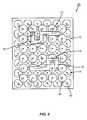
- FIG. 5illustrates an alternate embodiment with square overlapping plates
- FIG. 6illustrates another alternate embodiment with triangular overlapping plates
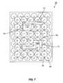
- FIG. 7illustrates a third alternate embodiment with hexagonal overlapping plates.
- the present inventionis preferably incorporated in a mobile terminal 20 , such as a cellular telephone, personal digital assistant, or the like.
- the basic architecture of a mobile terminal 20is represented in FIG. 1 and may include a receiver front end 22 , a radio frequency transmitter section 24 , an antenna 26 , a duplexer or switch 28 , a baseband processor 30 , a control system 32 , a frequency synthesizer 34 , and an interface 36 .
- the receiver front end 22receives information bearing radio frequency signals from one or more remote transmitters provided by a base station.
- a low noise amplifier 38amplifies the signal.
- a filter circuit 40minimizes broadband interference in the received signal, while downconversion and digitization circuitry 42 downconverts the filtered, received signal to an intermediate or baseband frequency signal, which is then digitized into one or more digital streams.
- the receiver front end 22typically uses one or more mixing frequencies generated by the frequency synthesizer 34 .
- the baseband processor 30processes the digitized received signal to extract the information or data bits conveyed in the received signal. This processing typically comprises demodulation, decoding, and error correction operations. As such, the baseband processor 30 is generally implemented in one or more digital signal processors (DSPs).
- DSPsdigital signal processors
- the baseband processor 30receives digitized data, which may represent voice, data, or control information, from the control system 32 , which it encodes for transmission.
- the encoded datais output to the radio frequency transmitter section 24 , where it is used by a modulator 44 to modulate a carrier signal that is at a desired transmit frequency.
- Power amplifier circuitry 46amplifies the modulated carrier signal to a level appropriate for transmission from the antenna 26 .
- the amplified signalis sent to the switch 28 and antenna 26 through an impedance matching circuit 48 , which is configured to set the overall load impedance for the amplifier circuitry 46 to optimize values based on the type or speed of information being transmitted.
- the switch 28 and antenna 26provide a relatively constant load impedance, which is combined with the impedance of the impedance matching circuit 48 to establish an overall load impedance for the amplifier circuitry 46 .
- Receiver front end 22 , the radio frequency transmitter section 24 , the frequency synthesizer 34 , the baseband processor 30 , and the control system 32are sometimes referred to herein as the transceiver circuitry. Since the operation of this circuitry is well understood for those of ordinary skill in the art, any further discussion is omitted.
- a usermay interact with the mobile terminal 20 via the interface 36 , which may include interface circuitry 52 associated with a microphone 54 , a speaker 56 , a keypad 58 , and a display 60 .
- the interface circuitry 52typically includes analog-to-digital converters, digital-to-analog converters, amplifiers, and the like. Additionally, it may include a voice encoder/decoder, in which case it may communicate directly with the baseband processor 30 .
- the microphone 54will typically convert audio input, such as the user's voice, into an electrical signal, which is then digitized and passed directly or indirectly to the baseband processor 30 . Audio information encoded in the received signal is recovered by the baseband processor 30 , and converted into an analog signal suitable for driving speaker 56 by the I/O and interface circuitry 52 .
- the keypad 58 and display 60enable the user to interact with the mobile terminal 20 , such as inputting numbers to be dialed, address book information, or the like, as well as monitor call progress information.
- a global positioning satellite (GPS) receivermay be integrated into the mobile terminal 20 .
- GPSglobal positioning satellite
- a Bluetooth modulemay be integrated into the mobile terminal 20 along with other short-range communication circuits, such as an IR circuit.
- the mobile terminal 20operates according to conventional telecommunications standards such as GSM, AMPS, D-AMPS, and other similar international telecommunications standards as needed or desired.
- FIG. 2illustrates one embodiment of the present invention wherein the antenna 26 is seen positioned over a substrate structure 70 .
- antenna 26comprises a first radiating element 72 and a second radiating element 74 .
- First and second radiating elements 72 , 74may be used together for diversity reception and transmission, or the first radiating element 72 may be used for transmission and the second radiating element 74 may be used for reception. Greater or lesser numbers of radiating elements may be used as needed or desired.
- the radiating elements 72 , 74each comprise a u-shaped kink 76 and are positioned over a first ground plane 78 .
- the first ground plane 78is comprised of two distinct levels of overlapping conductive plates 80 , 82 (better seen in FIG. 3 ).
- the overlapping conductive plates 80 , 82are arranged in two distinct levels to reduce eddy currents within the first ground plane 78 and help provide directionality for the radiating elements 72 , 74 as explained in the incorporated '495 patent.
- the u-shaped kink 76may be used to extend the electrical length of the radiating elements 72 , 74 , thereby effectively tuning the antenna 26 .
- the kink 76may also be used for impedance matching, or to provide dual band functionality for the antenna 26 .
- the kink 76adds inductive loading to the radiating elements 72 , 74 while also increasing the capacitive coupling between the radiating elements 72 , 74 and the first ground plane 78 .
- the kink 76may be an electric short (i.e., the electromagnetic current on the radiating elements 72 , 74 couples across the kink 76 rather than passing around the kink 76 ) at certain frequencies, thus creating a short antenna 26 at one frequency where the kink is shorted and a longer antenna 26 at other frequencies where the kink 76 is not bypassed.
- Geometries other than the kink 76may be used as needed or desired.
- the substrate structure 70is also illustrated in FIG. 3, wherein the layered relationship of the various components is better illustrated.
- the substrate structure 70comprises the antenna 26 , the first ground plane 78 , a second ground plane 84 , and an RF circuit element 86 .
- Distinct plies 88 of dielectric material 88 A, 88 B, 88 C, and 88 Dseparate the various electric components.
- the plies 88are formed from FR 4 .
- Other dielectric materialsmay also be used, and material type may vary between plies 88 if needed or desired.
- the RF circuit element 86may comprise as much of the transceiver circuitry as needed or desired.
- the RF circuit element 86comprises at least the duplexer 28 , and may also comprise the radio frequency transmitter section 24 and the receiver front end 22 .
- the frequency synthesizer 34 and baseband processor 30may be considered an RF circuit element 86 for the purposes of the present invention.
- the RF circuit element 86is printed or mounted on the ply 88 D using conventional integrated circuit printing technology, or is mounted thereon using conventional fabrication techniques.
- the antenna 26may be electrically connected to the RF circuit element 86 using any appropriate electrical connections.
- a through-hole via 90is used to connect the antenna 26 to the RF circuit element 86 .
- Other via connectorsmay also be used so long as the electrical connection therebetween is not shorted by inadvertent contact with either the first ground plane 78 or the second ground plane 84 .
- the first ground plane 78is electrically connected to the second ground plane 84 using via connectors 92 as is explained in the incorporated '495 patent.
- the second ground plane 84acts as a ground plane for any of the electronic components of the RF circuit element 86 as would be well understood. Thus, electrical connections may exist between RF circuit element 86 and the second ground plane 84 as needed or desired.
- the two distinct levels of overlapping conductive plates 80 , 82are illustrated in FIG. 2 as octagons. Please note that other polygonal and irregular shapes are contemplated. Specifically, triangles, hexagons, squares and circles are also acceptable plate shapes (see FIGS. 5 - 7 ).
- the octagonal shapes illustrateddo allow for spaces therebetween such that the through-hole via 90 may pass therethrough without intersecting either set of plates 80 , 82 . If the through-hole via 90 does pass through a plate 80 , 82 , clearances must be made so as to avoid a short circuit therebetween.
- the substrate structure 70is well-suited for incorporation into a mobile terminal 20 in that a single modular substrate structure 70 may have a footprint not much larger than one and one half inches squared (3.81 cm ⁇ 3.81 cm).
- the size of the radiating elements 72 , 74may be varied according to the desired operating frequencies.
- This modular structurehas the antenna 26 , a ground plane, and as much of the transceiver circuitry as desired for easy incorporation into a mobile terminal 20 .
- a second embodimentrelies on inverted F radiating elements 72 A, 74 A as illustrated in FIG. 4 .
- the placement of the radiating elements 72 A, 74 A relative to one anothermay be varied to provide for optimal matching and minimal crosstalk as needed or desired.
- the radiating elements 72 A, 74 Amight be rotated in the plane in which they lie so that the bars of the F both faced in, if desired.
- Other configurationsare likewise within the scope of the present invention.
Landscapes
- Engineering & Computer Science (AREA)
- Computer Networks & Wireless Communication (AREA)
- Physics & Mathematics (AREA)
- Optics & Photonics (AREA)
- Support Of Aerials (AREA)
- Transceivers (AREA)
Abstract
Description
Claims (20)
Priority Applications (1)
| Application Number | Priority Date | Filing Date | Title |
|---|---|---|---|
| US10/133,794US6657592B2 (en) | 2002-04-26 | 2002-04-26 | Patch antenna |
Applications Claiming Priority (1)
| Application Number | Priority Date | Filing Date | Title |
|---|---|---|---|
| US10/133,794US6657592B2 (en) | 2002-04-26 | 2002-04-26 | Patch antenna |
Publications (2)
| Publication Number | Publication Date |
|---|---|
| US20030201938A1 US20030201938A1 (en) | 2003-10-30 |
| US6657592B2true US6657592B2 (en) | 2003-12-02 |
Family
ID=29249055
Family Applications (1)
| Application Number | Title | Priority Date | Filing Date |
|---|---|---|---|
| US10/133,794Expired - LifetimeUS6657592B2 (en) | 2002-04-26 | 2002-04-26 | Patch antenna |
Country Status (1)
| Country | Link |
|---|---|
| US (1) | US6657592B2 (en) |
Cited By (49)
| Publication number | Priority date | Publication date | Assignee | Title |
|---|---|---|---|---|
| US6831506B1 (en) | 2003-09-17 | 2004-12-14 | Rf Micro Devices, Inc. | Reconfigurable filter architecture |
| US20050134506A1 (en)* | 2003-12-23 | 2005-06-23 | 3M Innovative Properties Company | Ultra high frequency radio frequency identification tag |
| US20050143026A1 (en)* | 2003-12-31 | 2005-06-30 | Wj Communications, Inc. | Integrated switching device for routing radio frequency signals |
| US20050231367A1 (en)* | 2003-12-31 | 2005-10-20 | Wj Communications, Inc. | Multiprotocol RFID reader |
| US20050243527A1 (en)* | 2004-04-29 | 2005-11-03 | Harris Corporation | Printed wiring board with enhanced structural integrity |
| US7033961B1 (en) | 2003-07-15 | 2006-04-25 | Rf Micro Devices, Inc. | Epitaxy/substrate release layer |
| WO2007005420A1 (en)* | 2005-07-01 | 2007-01-11 | Hrl Laboratories, Llc | Artificial impedance structure |
| US20070030661A1 (en)* | 2005-08-08 | 2007-02-08 | Rf Micro Devices, Inc. | Conformal electromagnetic interference shield |
| US20070236390A1 (en)* | 2006-04-06 | 2007-10-11 | Tatung Company | Dual-band circularly polarized antenna |
| US20070273607A1 (en)* | 2004-01-26 | 2007-11-29 | Agency For Science, Technology And Research | Compact Multi-Tiered Plate Antenna Arrays |
| US20080055045A1 (en)* | 2006-08-31 | 2008-03-06 | 3M Innovative Properties Company | Rfid tag including a three-dimensional antenna |
| US20080265038A1 (en)* | 2004-07-23 | 2008-10-30 | Fractus, S.A. | Antenna in Package with Reduced Electromagnetic Interaction with on Chip Elements |
| US20090002971A1 (en)* | 2007-06-27 | 2009-01-01 | Rf Micro Devices, Inc. | Bottom side support structure for conformal shielding process |
| US20090085750A1 (en)* | 2007-09-27 | 2009-04-02 | 3M Innovative Properties Company | Extended RFID tag |
| US20090085746A1 (en)* | 2007-09-27 | 2009-04-02 | 3M Innovative Properties Company | Signal line structure for a radio-frequency identification system |
| US20090096696A1 (en)* | 2007-10-11 | 2009-04-16 | Joyce Jr Terrence H | Rfid tag with a modified dipole antenna |
| US7546089B2 (en) | 2004-12-23 | 2009-06-09 | Triquint Semiconductor, Inc. | Switchable directional coupler for use with RF devices |
| US20090207027A1 (en)* | 2008-02-14 | 2009-08-20 | Banerjee Swagata R | Radio frequency identification (rfid) tag including a three-dimensional loop antenna |
| US20100149060A1 (en)* | 2008-12-12 | 2010-06-17 | National Taiwan University | Antenna module and design method thereof |
| US20100265152A1 (en)* | 2009-04-15 | 2010-10-21 | Samsung Electronics Co. Ltd. | Multi-band antenna apparatus |
| US8053872B1 (en) | 2007-06-25 | 2011-11-08 | Rf Micro Devices, Inc. | Integrated shield for a no-lead semiconductor device package |
| US8062930B1 (en) | 2005-08-08 | 2011-11-22 | Rf Micro Devices, Inc. | Sub-module conformal electromagnetic interference shield |
| US8835226B2 (en) | 2011-02-25 | 2014-09-16 | Rf Micro Devices, Inc. | Connection using conductive vias |
| US8959762B2 (en) | 2005-08-08 | 2015-02-24 | Rf Micro Devices, Inc. | Method of manufacturing an electronic module |
| US8988097B2 (en) | 2012-08-24 | 2015-03-24 | Rf Micro Devices, Inc. | Method for on-wafer high voltage testing of semiconductor devices |
| US9070761B2 (en) | 2012-08-27 | 2015-06-30 | Rf Micro Devices, Inc. | Field effect transistor (FET) having fingers with rippled edges |
| US9093420B2 (en) | 2012-04-18 | 2015-07-28 | Rf Micro Devices, Inc. | Methods for fabricating high voltage field effect transistor finger terminations |
| US9124221B2 (en) | 2012-07-16 | 2015-09-01 | Rf Micro Devices, Inc. | Wide bandwidth radio frequency amplier having dual gate transistors |
| US9129802B2 (en) | 2012-08-27 | 2015-09-08 | Rf Micro Devices, Inc. | Lateral semiconductor device with vertical breakdown region |
| US9137934B2 (en) | 2010-08-18 | 2015-09-15 | Rf Micro Devices, Inc. | Compartmentalized shielding of selected components |
| US9142620B2 (en) | 2012-08-24 | 2015-09-22 | Rf Micro Devices, Inc. | Power device packaging having backmetals couple the plurality of bond pads to the die backside |
| US20150270622A1 (en)* | 2014-03-20 | 2015-09-24 | Canon Kabushiki Kaisha | Antenna device |
| US9147632B2 (en) | 2012-08-24 | 2015-09-29 | Rf Micro Devices, Inc. | Semiconductor device having improved heat dissipation |
| US9202874B2 (en) | 2012-08-24 | 2015-12-01 | Rf Micro Devices, Inc. | Gallium nitride (GaN) device with leakage current-based over-voltage protection |
| US9325281B2 (en) | 2012-10-30 | 2016-04-26 | Rf Micro Devices, Inc. | Power amplifier controller |
| US9455327B2 (en) | 2014-06-06 | 2016-09-27 | Qorvo Us, Inc. | Schottky gated transistor with interfacial layer |
| US9536803B2 (en) | 2014-09-05 | 2017-01-03 | Qorvo Us, Inc. | Integrated power module with improved isolation and thermal conductivity |
| US9627230B2 (en) | 2011-02-28 | 2017-04-18 | Qorvo Us, Inc. | Methods of forming a microshield on standard QFN package |
| US9807890B2 (en) | 2013-05-31 | 2017-10-31 | Qorvo Us, Inc. | Electronic modules having grounded electromagnetic shields |
| US9917080B2 (en) | 2012-08-24 | 2018-03-13 | Qorvo US. Inc. | Semiconductor device with electrical overstress (EOS) protection |
| US10062684B2 (en) | 2015-02-04 | 2018-08-28 | Qorvo Us, Inc. | Transition frequency multiplier semiconductor device |
| CN109586007A (en)* | 2018-10-26 | 2019-04-05 | 西安电子科技大学 | Planar tracks angular momentum antenna based on Butler matrix |
| US10312596B2 (en) | 2013-01-17 | 2019-06-04 | Hrl Laboratories, Llc | Dual-polarization, circularly-polarized, surface-wave-waveguide, artificial-impedance-surface antenna |
| US10615158B2 (en) | 2015-02-04 | 2020-04-07 | Qorvo Us, Inc. | Transition frequency multiplier semiconductor device |
| US10983194B1 (en) | 2014-06-12 | 2021-04-20 | Hrl Laboratories, Llc | Metasurfaces for improving co-site isolation for electronic warfare applications |
| US11058038B2 (en) | 2018-06-28 | 2021-07-06 | Qorvo Us, Inc. | Electromagnetic shields for sub-modules |
| US11114363B2 (en) | 2018-12-20 | 2021-09-07 | Qorvo Us, Inc. | Electronic package arrangements and related methods |
| US11127689B2 (en) | 2018-06-01 | 2021-09-21 | Qorvo Us, Inc. | Segmented shielding using wirebonds |
| US11515282B2 (en) | 2019-05-21 | 2022-11-29 | Qorvo Us, Inc. | Electromagnetic shields with bonding wires for sub-modules |
Families Citing this family (8)
| Publication number | Priority date | Publication date | Assignee | Title |
|---|---|---|---|---|
| TW571161B (en)* | 2002-07-30 | 2004-01-11 | Au Optronics Corp | A flat panel display in which a digitizer is integrated |
| US7627250B2 (en)* | 2006-08-16 | 2009-12-01 | Corning Cable Systems Llc | Radio-over-fiber transponder with a dual-band patch antenna system |
| USD592193S1 (en)* | 2007-08-21 | 2009-05-12 | Yokowo Co., Ltd. | Antenna substrate |
| KR20110062100A (en)* | 2009-12-02 | 2011-06-10 | 엘지전자 주식회사 | Antenna device and mobile terminal including same |
| GB2515769A (en)* | 2013-07-02 | 2015-01-07 | Roke Manor Research | A guiding medium |
| CN210074170U (en)* | 2017-04-03 | 2020-02-14 | 株式会社村田制作所 | High frequency module |
| JP7325303B2 (en)* | 2019-11-08 | 2023-08-14 | 加賀Fei株式会社 | wireless module |
| TWD214869S (en)* | 2021-01-08 | 2021-10-21 | 佳邦科技股份有限公司 | antenna |
Citations (7)
| Publication number | Priority date | Publication date | Assignee | Title |
|---|---|---|---|---|
| US6166705A (en)* | 1999-07-20 | 2000-12-26 | Harris Corporation | Multi title-configured phased array antenna architecture |
| US6262495B1 (en) | 1998-03-30 | 2001-07-17 | The Regents Of The University Of California | Circuit and method for eliminating surface currents on metals |
| US6300907B1 (en)* | 2000-01-25 | 2001-10-09 | Badger Meter, Inc. | Antenna assembly for subsurface meter pits |
| US6426722B1 (en)* | 2000-03-08 | 2002-07-30 | Hrl Laboratories, Llc | Polarization converting radio frequency reflecting surface |
| US6469673B2 (en)* | 2000-06-30 | 2002-10-22 | Nokia Mobile Phones Ltd. | Antenna circuit arrangement and testing method |
| US6483481B1 (en)* | 2000-11-14 | 2002-11-19 | Hrl Laboratories, Llc | Textured surface having high electromagnetic impedance in multiple frequency bands |
| US6552686B2 (en)* | 2001-09-14 | 2003-04-22 | Nokia Corporation | Internal multi-band antenna with improved radiation efficiency |
- 2002
- 2002-04-26USUS10/133,794patent/US6657592B2/ennot_activeExpired - Lifetime
Patent Citations (7)
| Publication number | Priority date | Publication date | Assignee | Title |
|---|---|---|---|---|
| US6262495B1 (en) | 1998-03-30 | 2001-07-17 | The Regents Of The University Of California | Circuit and method for eliminating surface currents on metals |
| US6166705A (en)* | 1999-07-20 | 2000-12-26 | Harris Corporation | Multi title-configured phased array antenna architecture |
| US6300907B1 (en)* | 2000-01-25 | 2001-10-09 | Badger Meter, Inc. | Antenna assembly for subsurface meter pits |
| US6426722B1 (en)* | 2000-03-08 | 2002-07-30 | Hrl Laboratories, Llc | Polarization converting radio frequency reflecting surface |
| US6469673B2 (en)* | 2000-06-30 | 2002-10-22 | Nokia Mobile Phones Ltd. | Antenna circuit arrangement and testing method |
| US6483481B1 (en)* | 2000-11-14 | 2002-11-19 | Hrl Laboratories, Llc | Textured surface having high electromagnetic impedance in multiple frequency bands |
| US6552686B2 (en)* | 2001-09-14 | 2003-04-22 | Nokia Corporation | Internal multi-band antenna with improved radiation efficiency |
Non-Patent Citations (1)
| Title |
|---|
| Broas, Romulo F. Jimenez, Sievenpiper, Daniel F., and Yablonovitch, Eli, "A High-Impedence Ground Plane Applied to a Cellphone Handset Geometry," IEEE Transactions on Microwave Theory and Techniques, vol. 49, No. 7, Jul. 2001, pp. 1262-1265. |
Cited By (105)
| Publication number | Priority date | Publication date | Assignee | Title |
|---|---|---|---|---|
| US7033961B1 (en) | 2003-07-15 | 2006-04-25 | Rf Micro Devices, Inc. | Epitaxy/substrate release layer |
| US6831506B1 (en) | 2003-09-17 | 2004-12-14 | Rf Micro Devices, Inc. | Reconfigurable filter architecture |
| US20050134506A1 (en)* | 2003-12-23 | 2005-06-23 | 3M Innovative Properties Company | Ultra high frequency radio frequency identification tag |
| CN100464349C (en)* | 2003-12-23 | 2009-02-25 | 3M创新有限公司 | Ultrahigh frequency radio frequency identification tag |
| US7215295B2 (en) | 2003-12-23 | 2007-05-08 | 3M Innovative Properties Company | Ultra high frequency radio frequency identification tag |
| US6999028B2 (en)* | 2003-12-23 | 2006-02-14 | 3M Innovative Properties Company | Ultra high frequency radio frequency identification tag |
| US20060044192A1 (en)* | 2003-12-23 | 2006-03-02 | 3M Innovative Properties Company | Ultra high frequency radio frequency identification tag |
| US7197279B2 (en)* | 2003-12-31 | 2007-03-27 | Wj Communications, Inc. | Multiprotocol RFID reader |
| US20050231367A1 (en)* | 2003-12-31 | 2005-10-20 | Wj Communications, Inc. | Multiprotocol RFID reader |
| US20050143026A1 (en)* | 2003-12-31 | 2005-06-30 | Wj Communications, Inc. | Integrated switching device for routing radio frequency signals |
| US7239858B2 (en)* | 2003-12-31 | 2007-07-03 | Wj Communications, Inc. | Integrated switching device for routing radio frequency signals |
| US7369098B2 (en)* | 2004-01-26 | 2008-05-06 | Agency For Science Technology And Research | Compact multi-tiered plate antenna arrays |
| US20070273607A1 (en)* | 2004-01-26 | 2007-11-29 | Agency For Science, Technology And Research | Compact Multi-Tiered Plate Antenna Arrays |
| US20050243527A1 (en)* | 2004-04-29 | 2005-11-03 | Harris Corporation | Printed wiring board with enhanced structural integrity |
| US7907417B2 (en) | 2004-04-29 | 2011-03-15 | Harris Corporation | Printed circuit board (PCB)with enhanced structural integrity |
| US7948766B2 (en) | 2004-04-29 | 2011-05-24 | Harris Corporation | Method of making printed wiring board with enhanced structural integrity |
| US7342801B2 (en)* | 2004-04-29 | 2008-03-11 | Harris Corporation | Printed wiring board with enhanced structural integrity |
| US7499287B2 (en) | 2004-04-29 | 2009-03-03 | Harris Corporation | Printed wiring board with enhanced structural integrity |
| US20080106475A1 (en)* | 2004-04-29 | 2008-05-08 | Harris Corporation | Printed wiring board with enhanced structural integrity |
| US20080245552A1 (en)* | 2004-04-29 | 2008-10-09 | Harris Corporation | Printed wiring board with enhanced structural integrity |
| US8330259B2 (en) | 2004-07-23 | 2012-12-11 | Fractus, S.A. | Antenna in package with reduced electromagnetic interaction with on chip elements |
| US20080265038A1 (en)* | 2004-07-23 | 2008-10-30 | Fractus, S.A. | Antenna in Package with Reduced Electromagnetic Interaction with on Chip Elements |
| US7546089B2 (en) | 2004-12-23 | 2009-06-09 | Triquint Semiconductor, Inc. | Switchable directional coupler for use with RF devices |
| GB2443334A (en)* | 2005-07-01 | 2008-04-30 | Hrl Lab Llc | Artificial impedance structure |
| WO2007005420A1 (en)* | 2005-07-01 | 2007-01-11 | Hrl Laboratories, Llc | Artificial impedance structure |
| US7830310B1 (en) | 2005-07-01 | 2010-11-09 | Hrl Laboratories, Llc | Artificial impedance structure |
| US9661739B2 (en) | 2005-08-08 | 2017-05-23 | Qorvo Us, Inc. | Electronic modules having grounded electromagnetic shields |
| US8959762B2 (en) | 2005-08-08 | 2015-02-24 | Rf Micro Devices, Inc. | Method of manufacturing an electronic module |
| US7451539B2 (en) | 2005-08-08 | 2008-11-18 | Rf Micro Devices, Inc. | Method of making a conformal electromagnetic interference shield |
| US8062930B1 (en) | 2005-08-08 | 2011-11-22 | Rf Micro Devices, Inc. | Sub-module conformal electromagnetic interference shield |
| US20070030661A1 (en)* | 2005-08-08 | 2007-02-08 | Rf Micro Devices, Inc. | Conformal electromagnetic interference shield |
| US7315283B2 (en)* | 2006-04-06 | 2008-01-01 | Tatung Company | Dual-band circularly polarized antenna |
| US20070236390A1 (en)* | 2006-04-06 | 2007-10-11 | Tatung Company | Dual-band circularly polarized antenna |
| US20080055045A1 (en)* | 2006-08-31 | 2008-03-06 | 3M Innovative Properties Company | Rfid tag including a three-dimensional antenna |
| US8349659B1 (en) | 2007-06-25 | 2013-01-08 | Rf Micro Devices, Inc. | Integrated shield for a no-lead semiconductor device package |
| US8053872B1 (en) | 2007-06-25 | 2011-11-08 | Rf Micro Devices, Inc. | Integrated shield for a no-lead semiconductor device package |
| US8061012B2 (en) | 2007-06-27 | 2011-11-22 | Rf Micro Devices, Inc. | Method of manufacturing a module |
| US8720051B2 (en) | 2007-06-27 | 2014-05-13 | Rf Micro Devices, Inc. | Conformal shielding process using process gases |
| US20090002971A1 (en)* | 2007-06-27 | 2009-01-01 | Rf Micro Devices, Inc. | Bottom side support structure for conformal shielding process |
| US20090000114A1 (en)* | 2007-06-27 | 2009-01-01 | Rf Micro Devices, Inc. | Heat sink formed with conformal shield |
| US8614899B2 (en) | 2007-06-27 | 2013-12-24 | Rf Micro Devices, Inc. | Field barrier structures within a conformal shield |
| US20100199492A1 (en)* | 2007-06-27 | 2010-08-12 | Rf Micro Devices, Inc. | Conformal shielding employing segment buildup |
| US8434220B2 (en)* | 2007-06-27 | 2013-05-07 | Rf Micro Devices, Inc. | Heat sink formed with conformal shield |
| US8409658B2 (en) | 2007-06-27 | 2013-04-02 | Rf Micro Devices, Inc. | Conformal shielding process using flush structures |
| US8359739B2 (en) | 2007-06-27 | 2013-01-29 | Rf Micro Devices, Inc. | Process for manufacturing a module |
| US20110038136A1 (en)* | 2007-06-27 | 2011-02-17 | Rf Micro Devices, Inc. | Backside seal for conformal shielding process |
| US20090002970A1 (en)* | 2007-06-27 | 2009-01-01 | Rf Micro Devices, Inc. | Conformal shielding process using process gases |
| US20090025211A1 (en)* | 2007-06-27 | 2009-01-29 | Rf Micro Devices, Inc. | Isolated conformal shielding |
| US20090000815A1 (en)* | 2007-06-27 | 2009-01-01 | Rf Micro Devices, Inc. | Conformal shielding employing segment buildup |
| US20110235282A1 (en)* | 2007-06-27 | 2011-09-29 | Rf Micro Devices, Inc. | Conformal shielding process using process gases |
| US20090002969A1 (en)* | 2007-06-27 | 2009-01-01 | Rf Micro Devices, Inc. | Field barrier structures within a conformal shield |
| US20090000816A1 (en)* | 2007-06-27 | 2009-01-01 | Rf Micro Devices, Inc. | Conformal shielding process using flush structures |
| US20090002972A1 (en)* | 2007-06-27 | 2009-01-01 | Rf Micro Devices, Inc. | Backside seal for conformal shielding process |
| US8186048B2 (en) | 2007-06-27 | 2012-05-29 | Rf Micro Devices, Inc. | Conformal shielding process using process gases |
| US8296941B2 (en) | 2007-06-27 | 2012-10-30 | Rf Micro Devices, Inc. | Conformal shielding employing segment buildup |
| US8296938B2 (en) | 2007-06-27 | 2012-10-30 | Rf Micro Devices, Inc. | Method for forming an electronic module having backside seal |
| US8220145B2 (en) | 2007-06-27 | 2012-07-17 | Rf Micro Devices, Inc. | Isolated conformal shielding |
| US20090085750A1 (en)* | 2007-09-27 | 2009-04-02 | 3M Innovative Properties Company | Extended RFID tag |
| US8289163B2 (en) | 2007-09-27 | 2012-10-16 | 3M Innovative Properties Company | Signal line structure for a radio-frequency identification system |
| US20090085746A1 (en)* | 2007-09-27 | 2009-04-02 | 3M Innovative Properties Company | Signal line structure for a radio-frequency identification system |
| US8717244B2 (en) | 2007-10-11 | 2014-05-06 | 3M Innovative Properties Company | RFID tag with a modified dipole antenna |
| US20090096696A1 (en)* | 2007-10-11 | 2009-04-16 | Joyce Jr Terrence H | Rfid tag with a modified dipole antenna |
| US7982616B2 (en) | 2008-02-14 | 2011-07-19 | 3M Innovative Properties Company | Radio frequency identification (RFID) tag including a three-dimensional loop antenna |
| US7847697B2 (en) | 2008-02-14 | 2010-12-07 | 3M Innovative Properties Company | Radio frequency identification (RFID) tag including a three-dimensional loop antenna |
| US20090207027A1 (en)* | 2008-02-14 | 2009-08-20 | Banerjee Swagata R | Radio frequency identification (rfid) tag including a three-dimensional loop antenna |
| US20090207026A1 (en)* | 2008-02-14 | 2009-08-20 | Banerjee Swagata R | Radio frequency identification (rfid) tag including a three-dimensional loop antenna |
| US8188928B2 (en)* | 2008-12-12 | 2012-05-29 | National Taiwan University | Antenna module and design method thereof |
| US20100149060A1 (en)* | 2008-12-12 | 2010-06-17 | National Taiwan University | Antenna module and design method thereof |
| US20100265152A1 (en)* | 2009-04-15 | 2010-10-21 | Samsung Electronics Co. Ltd. | Multi-band antenna apparatus |
| US8203490B2 (en)* | 2009-04-15 | 2012-06-19 | Samsung Electronics Co., Ltd | Multi-band antenna apparatus |
| US9137934B2 (en) | 2010-08-18 | 2015-09-15 | Rf Micro Devices, Inc. | Compartmentalized shielding of selected components |
| US9420704B2 (en) | 2011-02-25 | 2016-08-16 | Qorvo Us, Inc. | Connection using conductive vias |
| US9942994B2 (en) | 2011-02-25 | 2018-04-10 | Qorvo Us, Inc. | Connection using conductive vias |
| US8835226B2 (en) | 2011-02-25 | 2014-09-16 | Rf Micro Devices, Inc. | Connection using conductive vias |
| US9627230B2 (en) | 2011-02-28 | 2017-04-18 | Qorvo Us, Inc. | Methods of forming a microshield on standard QFN package |
| US9093420B2 (en) | 2012-04-18 | 2015-07-28 | Rf Micro Devices, Inc. | Methods for fabricating high voltage field effect transistor finger terminations |
| US9136341B2 (en) | 2012-04-18 | 2015-09-15 | Rf Micro Devices, Inc. | High voltage field effect transistor finger terminations |
| US9564497B2 (en) | 2012-04-18 | 2017-02-07 | Qorvo Us, Inc. | High voltage field effect transitor finger terminations |
| US9124221B2 (en) | 2012-07-16 | 2015-09-01 | Rf Micro Devices, Inc. | Wide bandwidth radio frequency amplier having dual gate transistors |
| US8988097B2 (en) | 2012-08-24 | 2015-03-24 | Rf Micro Devices, Inc. | Method for on-wafer high voltage testing of semiconductor devices |
| US9142620B2 (en) | 2012-08-24 | 2015-09-22 | Rf Micro Devices, Inc. | Power device packaging having backmetals couple the plurality of bond pads to the die backside |
| US9202874B2 (en) | 2012-08-24 | 2015-12-01 | Rf Micro Devices, Inc. | Gallium nitride (GaN) device with leakage current-based over-voltage protection |
| US9147632B2 (en) | 2012-08-24 | 2015-09-29 | Rf Micro Devices, Inc. | Semiconductor device having improved heat dissipation |
| US9917080B2 (en) | 2012-08-24 | 2018-03-13 | Qorvo US. Inc. | Semiconductor device with electrical overstress (EOS) protection |
| US9640632B2 (en) | 2012-08-24 | 2017-05-02 | Qorvo Us, Inc. | Semiconductor device having improved heat dissipation |
| US9070761B2 (en) | 2012-08-27 | 2015-06-30 | Rf Micro Devices, Inc. | Field effect transistor (FET) having fingers with rippled edges |
| US9129802B2 (en) | 2012-08-27 | 2015-09-08 | Rf Micro Devices, Inc. | Lateral semiconductor device with vertical breakdown region |
| US9325281B2 (en) | 2012-10-30 | 2016-04-26 | Rf Micro Devices, Inc. | Power amplifier controller |
| US10312596B2 (en) | 2013-01-17 | 2019-06-04 | Hrl Laboratories, Llc | Dual-polarization, circularly-polarized, surface-wave-waveguide, artificial-impedance-surface antenna |
| US9807890B2 (en) | 2013-05-31 | 2017-10-31 | Qorvo Us, Inc. | Electronic modules having grounded electromagnetic shields |
| US20150270622A1 (en)* | 2014-03-20 | 2015-09-24 | Canon Kabushiki Kaisha | Antenna device |
| US9825369B2 (en)* | 2014-03-20 | 2017-11-21 | Canon Kabushiki Kaisha | Antenna device |
| US9455327B2 (en) | 2014-06-06 | 2016-09-27 | Qorvo Us, Inc. | Schottky gated transistor with interfacial layer |
| US10983194B1 (en) | 2014-06-12 | 2021-04-20 | Hrl Laboratories, Llc | Metasurfaces for improving co-site isolation for electronic warfare applications |
| US9536803B2 (en) | 2014-09-05 | 2017-01-03 | Qorvo Us, Inc. | Integrated power module with improved isolation and thermal conductivity |
| US10062684B2 (en) | 2015-02-04 | 2018-08-28 | Qorvo Us, Inc. | Transition frequency multiplier semiconductor device |
| US10615158B2 (en) | 2015-02-04 | 2020-04-07 | Qorvo Us, Inc. | Transition frequency multiplier semiconductor device |
| US11127689B2 (en) | 2018-06-01 | 2021-09-21 | Qorvo Us, Inc. | Segmented shielding using wirebonds |
| US11058038B2 (en) | 2018-06-28 | 2021-07-06 | Qorvo Us, Inc. | Electromagnetic shields for sub-modules |
| US11219144B2 (en) | 2018-06-28 | 2022-01-04 | Qorvo Us, Inc. | Electromagnetic shields for sub-modules |
| CN109586007A (en)* | 2018-10-26 | 2019-04-05 | 西安电子科技大学 | Planar tracks angular momentum antenna based on Butler matrix |
| CN109586007B (en)* | 2018-10-26 | 2020-10-09 | 西安电子科技大学 | Planar Orbital Angular Momentum Antenna Based on Butler Matrix |
| US11114363B2 (en) | 2018-12-20 | 2021-09-07 | Qorvo Us, Inc. | Electronic package arrangements and related methods |
| US11515282B2 (en) | 2019-05-21 | 2022-11-29 | Qorvo Us, Inc. | Electromagnetic shields with bonding wires for sub-modules |
| US12431457B2 (en) | 2019-05-21 | 2025-09-30 | Qorvo Us, Inc. | Electromagnetic shields with bonding wires for sub-modules |
Also Published As
| Publication number | Publication date |
|---|---|
| US20030201938A1 (en) | 2003-10-30 |
Similar Documents
| Publication | Publication Date | Title |
|---|---|---|
| US6657592B2 (en) | Patch antenna | |
| CN1201433C (en) | Folded dual frequency band antennas for wireless communicators | |
| KR100757506B1 (en) | Antenna device and radio communication device | |
| US8315576B2 (en) | Capacitive compensation of cascaded directional couplers | |
| CN1225092C (en) | Mobile communication system with multi-band antenna | |
| CN101512835B (en) | Multiband antenna arrangement | |
| KR101257615B1 (en) | Low profile, folded antenna assembly for handheld communication devices | |
| US20100060542A1 (en) | Multi-Band Antenna Arrangement | |
| US6686884B2 (en) | Microchip dual band antenna | |
| US20040137950A1 (en) | Built-in, multi band, multi antenna system | |
| US9577325B2 (en) | Compact radiating array for wireless handheld or portable devices | |
| US20070052599A1 (en) | Antenna device and radio communication terminal | |
| US20040207484A1 (en) | Triplexer systems and methods for use in wireless communications device | |
| US6198943B1 (en) | Parasitic dual band matching of an internal looped dipole antenna | |
| US20030025571A1 (en) | Complex high frequency components | |
| CN101981837A (en) | Antenna layout and test method | |
| CN1143447C (en) | Signal combining device and method for radio communication | |
| US20060238420A1 (en) | Multilayer pcb antenna | |
| US20090285262A1 (en) | Antenna apparatus of portable terminal | |
| JPH09121178A (en) | Portable telephone set and portable telephone system using it | |
| US6229485B1 (en) | Antenna device | |
| CN101080851A (en) | A two-module integrated antenna and radio | |
| US20050253761A1 (en) | Antenna assembly and a wireless telecommunication apparatus using the same | |
| US6697021B2 (en) | Double F antenna | |
| CN1788390B (en) | Improvements in or relating to wireless terminals |
Legal Events
| Date | Code | Title | Description |
|---|---|---|---|
| AS | Assignment | Owner name:RF MICRO DEVICES, INC., NORTH CAROLINA Free format text:ASSIGNMENT OF ASSIGNORS INTEREST;ASSIGNORS:DENING, DAVID;STEEL, VICTOR;REYNOLDS, LEONARD;REEL/FRAME:012848/0005 Effective date:20020424 | |
| STCF | Information on status: patent grant | Free format text:PATENTED CASE | |
| FPAY | Fee payment | Year of fee payment:4 | |
| FPAY | Fee payment | Year of fee payment:8 | |
| AS | Assignment | Owner name:BANK OF AMERICA, N.A., AS ADMINISTRATIVE AGENT, TE Free format text:NOTICE OF GRANT OF SECURITY INTEREST IN PATENTS;ASSIGNOR:RF MICRO DEVICES, INC.;REEL/FRAME:030045/0831 Effective date:20130319 | |
| AS | Assignment | Owner name:RF MICRO DEVICES, INC., NORTH CAROLINA Free format text:TERMINATION AND RELEASE OF SECURITY INTEREST IN PATENTS (RECORDED 3/19/13 AT REEL/FRAME 030045/0831);ASSIGNOR:BANK OF AMERICA, N.A., AS ADMINISTRATIVE AGENT;REEL/FRAME:035334/0363 Effective date:20150326 | |
| FPAY | Fee payment | Year of fee payment:12 | |
| AS | Assignment | Owner name:QORVO US, INC., NORTH CAROLINA Free format text:MERGER;ASSIGNOR:RF MICRO DEVICES, INC.;REEL/FRAME:039196/0941 Effective date:20160330 |