US6657418B2 - Parasitic power supply system for supplying operating power to a control device - Google Patents
Parasitic power supply system for supplying operating power to a control deviceDownload PDFInfo
- Publication number
- US6657418B2 US6657418B2US10/010,824US1082401AUS6657418B2US 6657418 B2US6657418 B2US 6657418B2US 1082401 AUS1082401 AUS 1082401AUS 6657418 B2US6657418 B2US 6657418B2
- Authority
- US
- United States
- Prior art keywords
- power
- coupled
- load
- terminal
- circuit
- Prior art date
- Legal status (The legal status is an assumption and is not a legal conclusion. Google has not performed a legal analysis and makes no representation as to the accuracy of the status listed.)
- Expired - Lifetime, expires
Links
- 230000003071parasitic effectEffects0.000titleclaimsdescription36
- 238000000034methodMethods0.000claimsabstractdescription12
- 239000003990capacitorSubstances0.000claimsdescription34
- 230000004913activationEffects0.000claimsdescription19
- 230000001105regulatory effectEffects0.000claimsdescription17
- 238000004804windingMethods0.000claimsdescription15
- 239000004020conductorSubstances0.000claimsdescription13
- 230000004044responseEffects0.000claimsdescription12
- 230000005669field effectEffects0.000claimsdescription10
- 230000003213activating effectEffects0.000claimsdescription8
- 230000015556catabolic processEffects0.000claimsdescription8
- 230000001276controlling effectEffects0.000claimsdescription7
- 230000008878couplingEffects0.000claimsdescription7
- 238000010168coupling processMethods0.000claimsdescription7
- 238000005859coupling reactionMethods0.000claimsdescription7
- 238000002955isolationMethods0.000claimsdescription4
- 238000012544monitoring processMethods0.000abstract1
- 238000010586diagramMethods0.000description10
- 238000009434installationMethods0.000description6
- 230000000903blocking effectEffects0.000description4
- 238000001816coolingMethods0.000description3
- 230000003247decreasing effectEffects0.000description3
- 238000010438heat treatmentMethods0.000description3
- 238000005057refrigerationMethods0.000description3
- 239000000758substrateSubstances0.000description3
- 238000004378air conditioningMethods0.000description2
- 230000008901benefitEffects0.000description2
- 238000009429electrical wiringMethods0.000description2
- 239000002184metalSubstances0.000description2
- 230000008569processEffects0.000description2
- 239000007787solidSubstances0.000description2
- 230000009849deactivationEffects0.000description1
- 230000007812deficiencyEffects0.000description1
- 238000011161developmentMethods0.000description1
- 230000018109developmental processEffects0.000description1
- 230000008030eliminationEffects0.000description1
- 238000003379elimination reactionMethods0.000description1
- 230000007613environmental effectEffects0.000description1
- 230000003993interactionEffects0.000description1
- 229910044991metal oxideInorganic materials0.000description1
- 150000004706metal oxidesChemical class0.000description1
- 230000004048modificationEffects0.000description1
- 238000012986modificationMethods0.000description1
- 239000004065semiconductorSubstances0.000description1
Images


Classifications
- H—ELECTRICITY
- H02—GENERATION; CONVERSION OR DISTRIBUTION OF ELECTRIC POWER
- H02M—APPARATUS FOR CONVERSION BETWEEN AC AND AC, BETWEEN AC AND DC, OR BETWEEN DC AND DC, AND FOR USE WITH MAINS OR SIMILAR POWER SUPPLY SYSTEMS; CONVERSION OF DC OR AC INPUT POWER INTO SURGE OUTPUT POWER; CONTROL OR REGULATION THEREOF
- H02M5/00—Conversion of AC power input into AC power output, e.g. for change of voltage, for change of frequency, for change of number of phases
- H02M5/02—Conversion of AC power input into AC power output, e.g. for change of voltage, for change of frequency, for change of number of phases without intermediate conversion into DC
- H02M5/04—Conversion of AC power input into AC power output, e.g. for change of voltage, for change of frequency, for change of number of phases without intermediate conversion into DC by static converters
- H02M5/22—Conversion of AC power input into AC power output, e.g. for change of voltage, for change of frequency, for change of number of phases without intermediate conversion into DC by static converters using discharge tubes with control electrode or semiconductor devices with control electrode
- H02M5/275—Conversion of AC power input into AC power output, e.g. for change of voltage, for change of frequency, for change of number of phases without intermediate conversion into DC by static converters using discharge tubes with control electrode or semiconductor devices with control electrode using devices of a triode or transistor type requiring continuous application of a control signal
- H02M5/293—Conversion of AC power input into AC power output, e.g. for change of voltage, for change of frequency, for change of number of phases without intermediate conversion into DC by static converters using discharge tubes with control electrode or semiconductor devices with control electrode using devices of a triode or transistor type requiring continuous application of a control signal using semiconductor devices only
- H—ELECTRICITY
- H02—GENERATION; CONVERSION OR DISTRIBUTION OF ELECTRIC POWER
- H02J—CIRCUIT ARRANGEMENTS OR SYSTEMS FOR SUPPLYING OR DISTRIBUTING ELECTRIC POWER; SYSTEMS FOR STORING ELECTRIC ENERGY
- H02J7/00—Circuit arrangements for charging or depolarising batteries or for supplying loads from batteries
- H02J7/007—Regulation of charging or discharging current or voltage
- H—ELECTRICITY
- H02—GENERATION; CONVERSION OR DISTRIBUTION OF ELECTRIC POWER
- H02M—APPARATUS FOR CONVERSION BETWEEN AC AND AC, BETWEEN AC AND DC, OR BETWEEN DC AND DC, AND FOR USE WITH MAINS OR SIMILAR POWER SUPPLY SYSTEMS; CONVERSION OF DC OR AC INPUT POWER INTO SURGE OUTPUT POWER; CONTROL OR REGULATION THEREOF
- H02M1/00—Details of apparatus for conversion
- H02M1/0003—Details of control, feedback or regulation circuits
- H02M1/0006—Arrangements for supplying an adequate voltage to the control circuit of converters
Definitions
- This inventionrelates generally to an improved system for providing power to a control device used to control application of electrical power to a load; and, more particularly, it relates to a parasitic control device powered by the electrical power to be applied to a load and arranged to provide regulated electrical power to a control device whether the load is actively powered or not.
- Simple control systems for controlling application of electrical power to load devicesare known.
- environmental control systemssuch as heating, cooling, ventilating, humidifying, and air conditioning devices are known to be subject to activation and deactivation control by thermostats, timers, humidistats, and the like.
- heating, cooling and air conditioning devicessimple bi-metal thermostatic switches have been utilized to directly control the application of electrical power to the device, and require no external power to the device and no external or auxiliary electrical power source to switch the load power.
- thermostatsare used to sense ambient temperatures of target atmospheres and function to turn on power to controlled furnaces when the sensed ambient temperatures are reduced below preset thresholds.
- Systemsare also known to utilize timers to maintain heating or cooling cycles operational for predetermined timed cycles.
- such systemscan include separate plenum temperature sensors to control the operation of associated blower fans to hold off activation until plenum temperatures are raised to predetermined levels. Such operation saves power until the systems are operative to move warmed air and minimizes movement of cool air and avoids feelings of cold drafts.
- plenum sensorsare also often used to maintain power to blower fans after controlled furnaces have been shut off to thereby efficiently capture and make use of residual plenum heat.
- sensor and/or control devicesto selectively control application of electrical power to many other types of loads. Examples include utilizing control devices to selectively control application of electrical power to refrigeration equipment in response to sensed ambient temperatures or other controlled parameters; to lighting equipment in response to timers or sensed levels of light; to fan equipment in response to timed or sensed ambient temperatures; to humidity control apparatus to add or reduce humidity in response to sensed ambient humidity conditions; to timer controls to selectively activate various loads; and to valve systems in response to sensed or controlled conditions, to name a few.
- Prior art systems of the type summarizedcharacteristically utilize a separate sources of power for the sensors or control devices than that provided to power the controlled loads.
- separate power sourcesapplied over separate wiring, are required.
- the separate power sourcesare required to be regulated, and are often at different voltage levels from that of the power source for the affected loads.
- separate wiring installations for providing power to the sensors or control devicesare required, such installations being separate from the electrical wiring utilized for providing power to the loads. In those installations where only load power electrical wiring is available, these requirements for separate wiring are unduly difficult and costly to provide.
- Prior art systemsoften require dc power, whereas many loads require ac power; and, as indicated, regulation of the dc power may be required; or alternatively, batteries may be required to provide power to the sensors or control devices.
- one or more timer circuits and associated switching logic circuitwere utilized to control the timing of disabling the back-to-back power FETs to allow power stealing from the load circuit to maintain the low voltage power source for the control device and a higher voltage supply for controlling the gates of the FETs.
- These relatively complex circuitsallow controlling various low levels of load voltages, for example up to about 24 volts ac or dc.
- Another prior art power “stealing” circuitutilized a power transformer with a primary current winding to provide power to a control device when power is applied to the load, and a primary voltage winding to provide power to the control device when the load is not powered. This type of configuration has limited utility because it places severe limitations on the range of load currents that can be handled, and characteristically the power transformer can be quite large in size.
- an improved parasitic control system and methodincludes a means or method process for parasitically diverting enough power from a source of load power to provide power to a control device that is utilized to control switching of the load power to the load when a sensed or control condition is determined to exist.
- the power that is divertedis insufficient to negatively impact the power supplied to the load and is operative whether the power is being applied to the load or not.
- the parasitic diversionis accomplished through operation of a bias means or method process that controls the operation of a transconductance means that carries the load power.
- the bias meansincludes a capacitor that is charged continuously through interaction of the bias means and the transconductance means.
- the capacitorprovides the source of voltage utilized by voltage regulator means to develop the regulated dc voltage that is supplied to provide power to the control device.
- the voltage regulatorcan be directly powered to provide a non-isolated output voltage, or can be indirectly powered to provide an isolated output voltage.
- the improved parasitic control system and method for parasitically developing a regulated dc voltage to power an associated control device directly from the ac load power sourceeliminates the need to provide a separate power source for the control device and minimizes the need for a separate wiring system to supply power to the control device.
- One feature of the inventionprovides a solid state switching circuit for controlling the application of power supply voltage from a power line to a load in response to control signals received from a control device, for example a thermostat, a timer, or various other control devices, including circuitry for parasitically diverting power from the load power that is to be switched.
- a control devicefor example a thermostat, a timer, or various other control devices, including circuitry for parasitically diverting power from the load power that is to be switched.
- a pair of power FETsare coupled back-to-back in series with one power terminal and have a voltage limiting device coupled across the drains to allow utilization with a relatively high voltage power source.
- Bias circuitryis coupled to the common gate circuits to control the switching of the power FETs to a low impedance ON state to permit current flow to the load when load powering is activated by a control device, or a high impedance OFF state during which current is substantially blocked from the load.
- the bias circuitryalso permits the parasitic application of power from the load power source to maintain power for the control device. It is necessary to provide power to a control device power source when it is determined that the control device power source has decreased below a predetermined level, and is operative whether or not power to the load is activated.
- the parasitic use of load power to maintain the control device power source at a predetermined levelis insufficient to negatively affect the load power or affect operation of the load.
- Another feature of the inventionis to provide a regulated control device voltage from the control device power source.
- One embodimentprovides the regulated control device voltage directly to the control device.
- a second embodimentprovides isolation circuitry such that the regulated control device voltage applied to the control device is isolated from the switching and bias circuitry.
- FIG. 1is a simplified schematic block diagram of a Prior Art system that selectively provides power to a load in response to a sensed condition;
- FIG. 2is a simplified schematic block diagram of a Prior Art system that utilizes a transformer to steal power from the load power source to power a control device and to selectively provide power to a load;
- FIG. 3is a simplified schematic block diagram of a parasitic system for selectively providing power to an associated load in accordance with sensed or controlled conditions determined by a control device that is powered by the parasitic system;
- FIG. 4is a schematic diagram of one embodiment of the parasitic system embodying the present invention with alternative circuitry to provide either isolated output voltage or non-isolated output voltage for powering an associated control device;
- FIG. 5is a schematic diagram of a voltage regulator.
- FIG. 1is a simplified schematic block diagram of a Prior Art system that selectively provides power to a load in response to a sensed condition.
- a load 10is supplied ac load power from a source (not shown) that provides ac power at terminal 12 over conductor 14 to power switch 16 .
- the power switch 16provides the ac power on line 18 to load 10 when the power switch 16 is activated.
- the power returnis through load 10 via conductor 20 to terminal 22 .
- a control device 24which can be a sensor and/or a control circuit, is coupled by control line 26 to the power switch 16 .
- the control device 24receives its power from a source (not shown) that is coupled across terminals 28 and 30 .
- Load 10could be a blower in a furnace system, one or more lights, a fan in an exhaust system, a refrigeration system, valve controls, or any other type of load requiring controlled application of load power dependant upon a sensed and/or a controlled condition.
- power switch 16it is common for power switch 16 to be a power relay that may be selectively activated by the control device 24 .
- Control device 24could be a thermostat in a furnace system or refrigeration system, a light sensitive control in an electric light system, a temperature and/or humidity sensor in a fan system, a timer, pressure sensitive control used with valve controls, and so on.
- the control device 24it is common for the control device 24 to be separately wired and to require a separate source of power, which may or may not be required to be regulated, thereby increasing the cost and complexity of the system.
- FIG. 2is a simplified schematic block diagram of a Prior Art system that utilizes a transformer to steal power from the load power source to power a control device and to selectively provide power to a load.
- Load poweris provided at terminal 12 a and is available for selective application to load 10 a .
- the load poweris applied via line 14 a to power switch 16 a , which again can be a relay or other suitable switching device.
- Power transformer 19includes current windings 19 c and voltage windings 19 v .
- Load poweris applied on line 18 a to the current primary (not shown) of current transformer 19 c and the other terminal 19 cp of the primary current winding is coupled by line 18 b to load 10 a .
- the load poweris applied on line 14 b to the voltage primary winding, with the other voltage primary terminal 19 vp being coupled via line 18 b to load 10 a .
- the transformer secondary winding(not shown) provides power to the control device 24 a .
- the current winding 19 ccouples power to the transformer secondary winding when power switch 16 a is closed and the load 10 a is powered. There is little affect on the power to load 10 a .
- power switch 16 ais opened, a small current flows through the transformer voltage winding 19 v to couple power to the secondary winding. The small current has no affect on the load.
- the secondary voltage at line 19 sis directed to the rectifier and voltage regulator circuit 32 , which in turn provides the voltage to power the control device 24 a via line 34 .
- the system of the present inventionprovides substantial benefits over the operational limitations of the Prior Art described, and that it provides a system that can be utilized with a range of load power requirements, including substantially larger load power requirements than are available from other Prior Art power stealing circuits, while utilizing a less complex bias and control circuit.
- FIG. 3is a simplified schematic block diagram of a parasitic system for selectively providing power to an associated load in accordance with sensed or controlled conditions determined by a control device that is powered by the parasitic system.
- a parasitic control systemutilizes a minimal amount of electrical power provided to drive a load to develop electrical power for an associated control device.
- the system of “stealing” a small amount of load power in this parasitic mannerresults in elimination of the requirement of providing a separate source of power to drive the associated control device and eliminates the necessity of providing separate wiring to provide power from the separated power source.
- a load 34is supplied load power from an ac source (not shown) applied at terminal 36 .
- This poweris provided via electrical conductor 38 to parasitic controller 40 , which utilizes a small portion of such power to develop supply voltage to be provided via conductor 42 to provide power to control device 44 .
- Parasitic controller 40also passes the load power via conductor 46 to power switch 48 .
- Control device 44controls the operation of power switch 48 by control signals directed over conductor 50 to the power switch. When control device 44 determines that a controlling condition has been satisfied, a control signal is provided on conductor 50 to activate power switch 48 and the load power is provided via conductor 52 to load 34 , with the power return being through load 34 via conductor 54 to terminal 56 .
- the small portion of power diverted by the parasitic controller 40will not impair proper operation of load 34 except for low current loads of less than about 15 mA.
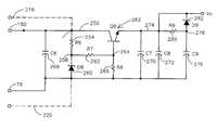
- FIG. 4is a schematic diagram of one embodiment of the parasitic system embodying the present invention.
- An alternating power sourcewhich can be in the range of about 24 Volts to about 240 Volts is applied at terminal 36 .
- This range of voltageis by way of example and is not intended as a limitation on the inventive concepts of the parasitic controller.
- a preferred embodiment for a system to control nominal ac load power of 240 voltswill be described.
- the input power signalis applied to diode D 1 58 to pass current in the direction of the diode arrow during forward bias of the ac power signal, and such current is applied via electrical conductor 60 to resistor R 1 62 , resistor R 2 64 , capacitor C 1 66 , and Zener diode D 2 68 .
- electrical conductorswill be referred to as ‘lines’.
- R 1 , R 2 , and R 3are nominally 100 k ohms, C 1 is 33 microfarads, and C 2 is 0.1 microfarads for this embodiment.
- R 1provides a voltage drop to junction 70 , which in turn is coupled via line 72 to the drain of field effect transistor (FET) Q 1 74 .
- FETfield effect transistor
- Common line 76is not earth ground, it being understood that with respect to earth ground, the entire circuit closely follows the voltage level of the power signal applied at terminal 36 . In this regard, common line 76 will be understood to float or follow as the circuit responds to applied power.
- Transistor Q 2 78is an npn transistor having its collector coupled at junction 80 to the gate of Q 1 and to load resistor R 2 , and has its emitter coupled to common line 76 .
- the base of Q 2is coupled through resistor R 3 82 to junction 84 .
- Capacitor C 1is coupled across line 60 and common line 76 .
- Zener diode D 2 68is coupled between line 60 and junction 84 and is selected to provide a predetermined reference voltage utilized to control the bias control for Q 2 .
- Capacitor C 2 86is coupled between junction 84 and common line 76 .
- the circuitry within dashed box 87forms a bias circuit that includes a voltage source to power an associated control device.
- Device U 1shown within dashed block 88 , is essentially a transconductance device made up of FET Q 3 90 , FET Q 4 92 , diode D 3 94 , and diode D 4 96 .
- Diodes D 3 and D 4are each shown as a separate device; however, in a preferred embodiment diode D 3 94 is a parasitic diode that exists between the substrate and the source of FET Q 3 90 , and diode D 4 96 is a parasitic diode that exists between the substrate and the source of FET Q 4 92 .
- the gates of Q 3 and Q 4are coupled together at junction 98 and by line 100 to junction 70 , where the bias control for U 1 is established.
- the source of Q 3 and the source of Q 4are coupled together at junction 102 to common line 76 .
- the drain of Q 3 and the blocking terminal of D 3are coupled to junction 104 , which in turn is coupled to junction 106 .
- the non-blocking terminal of D 3 and the drain of Q 3are coupled to junction 108 .
- the drain of Q 4 and the blocking terminal of D 4are coupled to junction 110 , which in turn is coupled to junction 112 .
- the non-blocking terminal of D 4 and the source of Q 4are coupled to junction 114 .
- Opposed breakdown diode D 5 116is coupled across junctions 106 and 112 and functions to limit the voltage applied across U 1 in both polarities.
- D 5is a limiting means that establishes nominally a limit of 15 volts.
- Diode D 6 118is coupled to junction 120 and via line 124 to junction 112 , and to junction 126 , with junction 126 being coupled to line 60 via line 128 .
- Diodes D 1 , D 3 , D 4 , and D 6function as a full-wave bridge rectifier when Q 3 and Q 4 are biased off.
- Capacitor C 1functions as a filter capacitor and as the voltage reference source to provide power to a control device.
- Diode D 2 , and transistors Q 1 and Q 2function to control FETs Q 3 and Q 4 to maintain C 1 charged to a regulated voltage level determined by Zener diode D 2 . This voltage is provided to either the isolated voltage regulator 206 or to the non-isolated voltage regulator 202
- the control of the application of power to output terminal 56 for application to a loadis accomplished by a controlled switch, such as relay K 1 shown as dashed block 130 , and has a normally-open contact 132 coupled to junction 134 , which in turn is coupled to junction 120 .
- Normally-closed contact 136is not connected.
- Wiper contact 138is coupled to junction 140 , which in turn is coupled to output terminal 56 .
- Capacitor C 3 142is coupled across junctions 134 and 140 and for this embodiment has a value of 0.033 microfarads 250 volts ac. Capacitor C 3 provides capacitive coupling through a load to the other side of the load power (not shown).
- the application of an activating signal across terminals 144 and 146will cause activation of coil terminals 148 and 150 , thereby causing wiper 138 to be switched and make contact with normally-open contact 132 .
- An optional control for relay K 1is shown within dashed block 160 and includes FET Q 5 162 , capacitor C 4 164 and resistor R 4 166 .
- the drain of Q 5is coupled to junction 168 to provide drive to terminal 150 for relay K 1 , and has its source coupled through junctions 170 and 172 to junction 174 , thereby connecting to common line 76 .
- the gate of Q 5is coupled through junction 176 to resistor R 5 178 , which in turn is coupled through junctions 180 and 172 power line 60 .
- Signals for terminal 148are derived from the R-C network of R 4 and C 4 , where C 4 is coupled across junctions 184 and 186 .
- Junction 186is coupled to junction 188
- junction 184is coupled to junction 190 to provide the signals to relay coil terminal 148 .
- a control device 200 for differing applicationscan be powered directly by voltage regulator 202 comprising a source of non-isolated voltage shown within dashed block 204 , or from an isolated voltage source shown within dashed block 206 .
- voltage regulator 202comprising a source of non-isolated voltage shown within dashed block 204
- isolated voltage sourceshown within dashed block 206
- the selection of an isolated voltage source or a non-isolated voltage sourcewill depend upon the nature of the control device used and the particular application, it being understood that either the isolated voltage source or the non-isolated voltage source, but not both, would be utilized for a particular application.
- voltage regulator 202is provided input signals through junctions 170 and 180 , and functions to provide non-isolated output voltage Vnio on line 208 to control device 200 .
- a form of voltage regulatorwill be described below.
- isolated voltage source 206utilizes an oscillator 210 that is coupled to junctions 126 and 172 and to the primary coil of transformer T 1 212 .
- the secondary windings of T 1are coupled across a pair of terminals for diode bridge rectifier network D 7 214 .
- a third terminal of the bridge 214is coupled via line 216 to voltage regulator 218 and to a terminal of capacitor C 5 224 .
- the fourth terminal of D 7is coupled via line 226 to the other terminal of C 5 and to the voltage regulator 218 via line 220 .
- C 5has a nominal value of 15 microfarads.
- Voltage regulator 218provides isolated output voltage Vio to control device 200 via line 222 .
- FIG. 5is a schematic diagram of a voltage regulator with alternative circuitry to provide either isolated output voltage or non-isolated output voltage for powering an associated control device. It will be seen that the voltage regulator circuits for the isolated and non-isolated configuration are the same, with the non-isolated configuration input shown in solid lines and the isolated configuration is shown in dashed line.
- resistor R 6 254which is coupled between junctions 256 and 258 ; Zener diode D 8 260 , which is coupled between junction 258 and circuit common line 76 ; resistor R 7 262 , which is coupled between junctions 258 and 264 ; and resistor R 8 266 , which is coupled between common line 76 , and through junction 264 to the base of Q 6 .
- a nominal value for R 6is 5.1 k ohms
- R 7is 3.9 k ohms
- R 8is 12 k ohms
- D 8sets a reference voltage.
- Capacitor C 6 268is coupled across line 250 and common line 76 , and is nominally 0.01 microfarads.
- the dc output voltage Vois derived from the emitter of Q 6 and is established by the output network that includes, capacitors C 7 270 and C 8 272 , both of which are coupled across line 274 and common line 76 ; capacitor C 9 276 , which is coupled between junction 278 and common line 76 ; resistor R 9 280 , which coupled is between junction 278 and output line 274 ; and low voltage drop schottky diode D 9 282 , which is coupled between junction 278 and output line 274 .
- the regulated voltage at Q 6 emitteris set by the values of D 8 , R 7 and R 8 .
- Capacitors C 7 and C 8are output filter capacitors.
- Resistor R 9 in conjunction with diode D 9limit the charging current for Capacitor C 9 . This allows control device 200 to start operating if capacitor C 9 is completely discharged. Capacitor C 9 is a supercapacitor that can keep the control device operating for several hours during a power outage. Nominally, C 7 is 15 microfarads, C 8 is 0.01 microfarads, C 9 is 0.33 farads, and R 9 is 3.01 k.
- the isolated voltage regulator configurationis identical, with the positive output from diode bridge network D 7 provided on dashed line 216 to junction 256 to provide a voltage signal to Q 6 .
- Dashed line 220provides the isolated common connection from the negative output of D 7 .
- ac load poweris nominally 240 volts ac. It is of course understood that for different sources of ac power and for different types of control devices, the values and arrangement of the various components may have to be adjusted, and that such adjustments are routine and will not depart from the inventive concepts. All of the components are available commercially.
- the FET usage in this embodimenthas similar operation to npn transistors, and in operation has the drain more positive than the source. No current flows from the drain to the source unless the gate is biased more positive than the source. When the gate is forward biased, drain current flows to the source.
- the FEThas practically no gate current resulting in extremely high input impedance. It also has high incremental drain impedance, resulting in nearly constant current when the drain-source bias voltage is greater than one or two volts.
- the drain currentcan be increased or decreased by either increasing or decreasing the gate-to-source bias, respectively.
- the FETis essentially a transconductance device, with gate-source voltage programming the drain current.
- MOSFETmetal oxide semiconductor field effect transistors
- the source of load power(not shown in FIG. 4) is applied at input terminal 36 , the load power passes through the circuitry that has been described, and when control device 200 indicates that power should be applied to a load, the power switch K 1 passes the load power to the load at output terminal 56 . The load power is then passed through the load to ground or common and completes the power circuit.
- the load poweris from an ac source and causes the voltage at terminal 36 to vary accordingly.
- Common line 76follows with respect to the variations of the applied ac load power.
- a bias voltageis developed at junction 84 that puts a bias on the base of Q 2 at a level to cause it to turn on.
- Q 2When Q 2 is biased on, it develops a bias voltage at junction 80 that biases the gate of FET Q 1 such that Q 1 is off.
- the bias control for transconductance device U 1is developed at junction 70 and is applied to the gates of U 1 transistors Q 3 and Q 4 at junction 98 .
- a bias voltageis developed at junction 98 from line 100 that is of a level to turn Q 3 and Q 4 on.
- Q 3 and Q 4are biased on, a low impedance path is developed between terminal 36 and line 124 .
- control device 200determines that load power is to be delivered to the load and the control terminals 148 and 150 are activated to cause relay K 1 to close and put wiper contact 138 in contact with terminal 132 , there is a direct connection between input terminal 36 and output terminal 56 to the load when Q 3 and Q 4 are biased on.
- Q 3 and Q 4are normally biased to be conducting, but are briefly biased off to charge C 1 .
- This interruption of the direct power connection between input 36 and output 56is very brief and is insufficient to negatively affect the supply of power to the load.
- Capacitor C 3is selected for current requirements of the control device and to limit current through the load to a level that the load remains off.
- bi-directional breakdown diode D 5is utilized to control to the maximum voltage drop across U 1 and the charging circuit. It also limits the allowable swing of voltages on common line 76 .
- the voltage charge on C 1is utilized to develop the output of the circuit that is provided as the input to either oscillator 210 or to voltage regulator 202 .
- both voltage regulator 202 and oscillator 210are each coupled to common line 76 .
- one or the other of the isolated or non-isolated sourceswould be used for any particular control device 200 utilized to control activation of the operation of K 1 to supply or not supply power to a load.
- the operation of the isolated supplyinvolves the circuit elements shown in dashed block 206 , and utilizes the voltage levels provided at juncture 172 to drive the oscillator with respect to the level established by common line 76 .
- Oscillators of this typeare known in the art, and function to provide an oscillating signal to the primary of transformer T 1 . This signal is passed to the secondary of T 1 , thereby providing the isolation, and is rectified by fall wave rectifier diode bridge D 7 . The signal provided on line 216 is directed to the voltage regulator 218 .
- the voltage inputis provided directly from C 1 at juncture 180 .
- Voltage regulator 202is also coupled to common line 76 , as shown in FIG. 5 .
- the operation of the voltage regulatoris such that the non-isolated voltage applied at junctures 180 and 76 is provided by C 1 , and the isolated voltage applied at junctures 216 and 228 is provided by C 5 .
- This voltage inis applied at juncture 256 to capacitor C 6 , the collector of Q 6 , and to the bias network made up of D 7 and resistors R 7 and R 8 , that controls the base bias of Q 6 .
- the bias networkwill cause Q 6 to conduct under control of the input voltage, but limited by the breakdown voltage of Zener diode D 8 which will limit the swing of the base bias.
- the output of Q 6is applied to filter capacitors C 7 and C 8 .
- Resistor R 9 in conjunction with diode D 9limit the charging current for capacitor C 9 .
- Capacitor C 9is a super capacitor that can keep the control device operating for several hours in the event of load power outage. In a characteristic embodiment Vo will be in the order of 3 volts dc, but can be adjusted to meet the needs of providing power to any particular control device.
- control device 200provides an activation signal to juncture 176 , which in turn is applied to the gate of Q 5 .
- the source of Q 5is coupled to common line 76 , and the drain is coupled to coil terminal 168 .
- the R-C network of R 4 and C 4is coupled to the other terminal 190 to be coupled to the activation coil of K 1 .
- Q 5is turned on when its gate is forward biased by the activation signal provided by the control device, thereby completing the circuit to provide activation power to the coil. It is of course understood that the control device could be utilized to activate relay coil terminals 148 and 150 directly to control operation of relay K 1 .
Landscapes
- Engineering & Computer Science (AREA)
- Power Engineering (AREA)
- Dc-Dc Converters (AREA)
- Direct Current Feeding And Distribution (AREA)
Abstract
Description
Claims (25)
Priority Applications (3)
| Application Number | Priority Date | Filing Date | Title |
|---|---|---|---|
| US10/010,824US6657418B2 (en) | 2001-11-13 | 2001-11-13 | Parasitic power supply system for supplying operating power to a control device |
| EP02780615AEP1444772A1 (en) | 2001-11-13 | 2002-11-12 | Power supply system for a control device |
| PCT/US2002/036162WO2003043171A1 (en) | 2001-11-13 | 2002-11-12 | Power supply system for a control device |
Applications Claiming Priority (1)
| Application Number | Priority Date | Filing Date | Title |
|---|---|---|---|
| US10/010,824US6657418B2 (en) | 2001-11-13 | 2001-11-13 | Parasitic power supply system for supplying operating power to a control device |
Publications (2)
| Publication Number | Publication Date |
|---|---|
| US20030090243A1 US20030090243A1 (en) | 2003-05-15 |
| US6657418B2true US6657418B2 (en) | 2003-12-02 |
Family
ID=21747618
Family Applications (1)
| Application Number | Title | Priority Date | Filing Date |
|---|---|---|---|
| US10/010,824Expired - LifetimeUS6657418B2 (en) | 2001-11-13 | 2001-11-13 | Parasitic power supply system for supplying operating power to a control device |
Country Status (3)
| Country | Link |
|---|---|
| US (1) | US6657418B2 (en) |
| EP (1) | EP1444772A1 (en) |
| WO (1) | WO2003043171A1 (en) |
Cited By (38)
| Publication number | Priority date | Publication date | Assignee | Title |
|---|---|---|---|---|
| US20040108773A1 (en)* | 2002-12-06 | 2004-06-10 | Strong Maurice Leroy | Capacitor and switch components cooperation to maintain input voltage to target circuit at or above cut-off voltage until power circuit is able to maintain the input voltage |
| US20040256915A1 (en)* | 2003-06-17 | 2004-12-23 | Phinney Thomas L. | Power supply apparatus and method based on parasitic power extraction |
| US20060255745A1 (en)* | 2005-05-12 | 2006-11-16 | Dejonge Stuart | Dimmer having a power supply monitoring circuit |
| US20090015072A1 (en)* | 2007-07-10 | 2009-01-15 | Bauer Martin L | Parasitic power supply for traffic control systems |
| US20100232193A1 (en)* | 2007-11-27 | 2010-09-16 | Koninklijke Philips Electronics N.V. | Capacitive power supply |
| US20110001485A1 (en)* | 2008-09-07 | 2011-01-06 | Feight Laurence V | Energy management for an electronic device |
| US20120092020A1 (en)* | 2010-10-18 | 2012-04-19 | Xin Zhou | Acoustic apparatus and acoustic sensor apparatus including a clamp |
| US8511577B2 (en) | 2011-02-24 | 2013-08-20 | Nest Labs, Inc. | Thermostat with power stealing delay interval at transitions between power stealing states |
| US8511576B2 (en) | 2011-02-24 | 2013-08-20 | Nest Labs, Inc. | Power management in energy buffered building control unit |
| US8523083B2 (en) | 2011-02-24 | 2013-09-03 | Nest Labs, Inc. | Thermostat with self-configuring connections to facilitate do-it-yourself installation |
| US8532827B2 (en) | 2011-10-21 | 2013-09-10 | Nest Labs, Inc. | Prospective determination of processor wake-up conditions in energy buffered HVAC control unit |
| US8627127B2 (en) | 2011-02-24 | 2014-01-07 | Nest Labs, Inc. | Power-preserving communications architecture with long-polling persistent cloud channel for wireless network-connected thermostat |
| US8659302B1 (en) | 2012-09-21 | 2014-02-25 | Nest Labs, Inc. | Monitoring and recoverable protection of thermostat switching circuitry |
| US8752771B2 (en) | 2010-11-19 | 2014-06-17 | Nest Labs, Inc. | Thermostat battery recharging during HVAC function active and inactive states |
| US9071145B2 (en) | 2008-07-29 | 2015-06-30 | Honeywell International Inc. | Power stealing circuitry for a control device |
| US9092039B2 (en) | 2010-11-19 | 2015-07-28 | Google Inc. | HVAC controller with user-friendly installation features with wire insertion detection |
| US9194600B2 (en) | 2004-10-06 | 2015-11-24 | Google Inc. | Battery charging by mechanical impeller at forced air vent outputs |
| US9268344B2 (en) | 2010-11-19 | 2016-02-23 | Google Inc. | Installation of thermostat powered by rechargeable battery |
| US9386529B2 (en) | 2012-09-06 | 2016-07-05 | Schweitzer Engineering Laboratories, Inc. | Power management in a network of stationary battery powered control, automation, monitoring and protection devices |
| US9396633B1 (en) | 2015-06-14 | 2016-07-19 | Google Inc. | Systems, methods, and devices for managing coexistence of multiple transceiver devices by optimizing component layout |
| US9448567B2 (en) | 2010-11-19 | 2016-09-20 | Google Inc. | Power management in single circuit HVAC systems and in multiple circuit HVAC systems |
| US9459018B2 (en) | 2010-11-19 | 2016-10-04 | Google Inc. | Systems and methods for energy-efficient control of an energy-consuming system |
| US9543998B2 (en) | 2015-06-14 | 2017-01-10 | Google Inc. | Systems, methods, and devices for managing coexistence of multiple transceiver devices using bypass circuitry |
| US9612031B2 (en) | 2015-01-07 | 2017-04-04 | Google Inc. | Thermostat switching circuitry robust against anomalous HVAC control line conditions |
| US9684316B2 (en) | 2013-04-05 | 2017-06-20 | Emerson Electric Co. | Controlling current for power stealing in climate control systems |
| US9794522B2 (en) | 2015-02-06 | 2017-10-17 | Google Inc. | Systems, methods, and devices for managing coexistence of multiple transceiver devices by optimizing component layout |
| US9804610B2 (en) | 2010-09-14 | 2017-10-31 | Google Inc. | Thermostat user interface |
| US9851728B2 (en) | 2010-12-31 | 2017-12-26 | Google Inc. | Inhibiting deleterious control coupling in an enclosure having multiple HVAC regions |
| US20180048300A1 (en)* | 2013-04-23 | 2018-02-15 | Honeywell International Inc. | Active triac triggering circuit |
| US10191501B2 (en) | 2012-03-01 | 2019-01-29 | Emerson Electric Co. | Systems and methods for power stealing |
| US10338613B2 (en) | 2016-03-02 | 2019-07-02 | Triune Systems, L.L.C. | Circuits and methods for providing power and data communication in isolated system architectures |
| US10459025B1 (en) | 2018-04-04 | 2019-10-29 | Schweitzer Engineering Laboratories, Inc. | System to reduce start-up times in line-mounted fault detectors |
| US10613213B2 (en) | 2016-05-13 | 2020-04-07 | Google Llc | Systems, methods, and devices for utilizing radar with smart devices |
| US10687184B2 (en) | 2016-05-13 | 2020-06-16 | Google Llc | Systems, methods, and devices for utilizing radar-based touch interfaces |
| US11105834B2 (en) | 2019-09-19 | 2021-08-31 | Schweitzer Engineering Laboratories, Inc. | Line-powered current measurement device |
| US20220116103A1 (en)* | 2020-10-09 | 2022-04-14 | Schweitzer Engineering Laboratories, Inc. | Wireless radio repeater for electric power distribution system |
| US11397198B2 (en) | 2019-08-23 | 2022-07-26 | Schweitzer Engineering Laboratories, Inc. | Wireless current sensor |
| US12184343B2 (en) | 2021-10-08 | 2024-12-31 | Schweitzer Engineering Laboratories, Inc. | Systems and methods to communicate data between devices of an electric power delivery system |
Families Citing this family (16)
| Publication number | Priority date | Publication date | Assignee | Title |
|---|---|---|---|---|
| AU2002951291A0 (en)* | 2002-09-09 | 2002-09-19 | Energy Storage Systems Pty Ltd | A power supply |
| WO2006022838A1 (en)* | 2004-08-11 | 2006-03-02 | Carrier Corporation | Improved power stealing for a thermostat using a triac with fet control |
| JP4725492B2 (en)* | 2006-04-04 | 2011-07-13 | 株式会社デンソー | Load control device and load control method |
| CN107065961B (en) | 2010-12-31 | 2020-06-16 | 谷歌有限责任公司 | Flexible functional partitioning of intelligent thermostat controlled HVAC systems |
| US9497828B2 (en)* | 2012-03-20 | 2016-11-15 | Koninklijke Philips Electronics N.V. | Two-wire flyback dimmer and a metod of operation thereof |
| US8708242B2 (en)* | 2012-09-21 | 2014-04-29 | Nest Labs, Inc. | Thermostat system with software-repurposable wiring terminals adaptable for HVAC systems of different ranges of complexity |
| US20150348722A1 (en)* | 2013-01-16 | 2015-12-03 | Legend Corporate Services Pty Ltd | Switching circuit |
| US9581342B2 (en) | 2014-03-28 | 2017-02-28 | Google Inc. | Mounting stand for multi-sensing environmental control device |
| US9568201B2 (en) | 2014-03-28 | 2017-02-14 | Google Inc. | Environmental control system retrofittable with multiple types of boiler-based heating systems |
| US9791839B2 (en) | 2014-03-28 | 2017-10-17 | Google Inc. | User-relocatable self-learning environmental control device capable of adapting previous learnings to current location in controlled environment |
| US9609462B2 (en) | 2014-03-28 | 2017-03-28 | Google Inc. | Facilitating radio frequency communications among environmental control system components |
| US9841203B2 (en)* | 2014-07-17 | 2017-12-12 | Emerson Electric Co. | Apparatus and methods for power stealing by controllers |
| CN104503524A (en)* | 2014-11-18 | 2015-04-08 | 北京七芯中创科技有限公司 | Circuit structure capable of selecting between external power supply and parasite power supply |
| US20160241157A1 (en)* | 2015-02-12 | 2016-08-18 | General Electric Company | Small power harvesting methods for powering control devices using a single power line |
| US10992175B2 (en) | 2018-06-15 | 2021-04-27 | Google Llc | Communication circuit for 2-wire protocols between HVAC systems and smart-home devices |
| US11742692B1 (en)* | 2019-12-13 | 2023-08-29 | Amazon Technologies, Inc. | Power stealing in relay circuits |
Citations (4)
| Publication number | Priority date | Publication date | Assignee | Title |
|---|---|---|---|---|
| US5736795A (en)* | 1996-04-22 | 1998-04-07 | Honeywell Inc. | Solid state AC switch with self-synchronizing means for stealing operating power |
| US5811963A (en)* | 1994-10-11 | 1998-09-22 | Novitas Incorporated | Line powered DC power supply |
| US5903139A (en) | 1997-01-27 | 1999-05-11 | Honeywell Inc. | Power stealing solid state switch for supplying operating power to an electronic control device |
| US6356038B2 (en)* | 1994-12-14 | 2002-03-12 | Richard A. Bishel | Microcomputer-controlled AC power switch controller and DC power supply method and apparatus |
Family Cites Families (3)
| Publication number | Priority date | Publication date | Assignee | Title |
|---|---|---|---|---|
| US4300090A (en)* | 1979-03-02 | 1981-11-10 | Weber Harold J | Direct current power supply |
| DE3537447A1 (en)* | 1985-10-22 | 1987-04-23 | Diehl Gmbh & Co | SUPPLY CIRCUIT |
| DE19927525A1 (en)* | 1999-06-16 | 2001-01-04 | Siemens Ag | Circuit for the power supply of a semiconductor switching device |
- 2001
- 2001-11-13USUS10/010,824patent/US6657418B2/ennot_activeExpired - Lifetime
- 2002
- 2002-11-12EPEP02780615Apatent/EP1444772A1/ennot_activeWithdrawn
- 2002-11-12WOPCT/US2002/036162patent/WO2003043171A1/ennot_activeApplication Discontinuation
Patent Citations (4)
| Publication number | Priority date | Publication date | Assignee | Title |
|---|---|---|---|---|
| US5811963A (en)* | 1994-10-11 | 1998-09-22 | Novitas Incorporated | Line powered DC power supply |
| US6356038B2 (en)* | 1994-12-14 | 2002-03-12 | Richard A. Bishel | Microcomputer-controlled AC power switch controller and DC power supply method and apparatus |
| US5736795A (en)* | 1996-04-22 | 1998-04-07 | Honeywell Inc. | Solid state AC switch with self-synchronizing means for stealing operating power |
| US5903139A (en) | 1997-01-27 | 1999-05-11 | Honeywell Inc. | Power stealing solid state switch for supplying operating power to an electronic control device |
Cited By (102)
| Publication number | Priority date | Publication date | Assignee | Title |
|---|---|---|---|---|
| US7112897B2 (en)* | 2002-12-06 | 2006-09-26 | Northrop Grumman Corporation | Capacitor and switch components cooperation to maintain input voltage to target circuit at or above cut-off voltage until power circuit is able to maintain the input voltage |
| US20040108773A1 (en)* | 2002-12-06 | 2004-06-10 | Strong Maurice Leroy | Capacitor and switch components cooperation to maintain input voltage to target circuit at or above cut-off voltage until power circuit is able to maintain the input voltage |
| US7291938B2 (en)* | 2003-06-17 | 2007-11-06 | Honeywell International Inc. | Power supply apparatus and method based on parasitic power extraction |
| US20040256915A1 (en)* | 2003-06-17 | 2004-12-23 | Phinney Thomas L. | Power supply apparatus and method based on parasitic power extraction |
| US9353964B2 (en) | 2004-10-06 | 2016-05-31 | Google Inc. | Systems and methods for wirelessly-enabled HVAC control |
| US10126011B2 (en) | 2004-10-06 | 2018-11-13 | Google Llc | Multiple environmental zone control with integrated battery status communications |
| US9353963B2 (en) | 2004-10-06 | 2016-05-31 | Google Inc. | Occupancy-based wireless control of multiple environmental zones with zone controller identification |
| US10215437B2 (en) | 2004-10-06 | 2019-02-26 | Google Llc | Battery-operated wireless zone controllers having multiple states of power-related operation |
| US9194600B2 (en) | 2004-10-06 | 2015-11-24 | Google Inc. | Battery charging by mechanical impeller at forced air vent outputs |
| US9618223B2 (en) | 2004-10-06 | 2017-04-11 | Google Inc. | Multi-nodal thermostat control system |
| US9316407B2 (en) | 2004-10-06 | 2016-04-19 | Google Inc. | Multiple environmental zone control with integrated battery status communications |
| US9995497B2 (en) | 2004-10-06 | 2018-06-12 | Google Llc | Wireless zone control via mechanically adjustable airflow elements |
| USRE42425E1 (en) | 2005-05-12 | 2011-06-07 | Lutron Electronics Co., Inc. | Dimmer having a power supply monitoring circuit |
| US7242150B2 (en) | 2005-05-12 | 2007-07-10 | Lutron Electronics Co., Inc. | Dimmer having a power supply monitoring circuit |
| US20060255745A1 (en)* | 2005-05-12 | 2006-11-16 | Dejonge Stuart | Dimmer having a power supply monitoring circuit |
| US7911084B2 (en) | 2007-07-10 | 2011-03-22 | Aldis Corporation | Parasitic power supply for traffic control systems |
| US20090015072A1 (en)* | 2007-07-10 | 2009-01-15 | Bauer Martin L | Parasitic power supply for traffic control systems |
| US20100232193A1 (en)* | 2007-11-27 | 2010-09-16 | Koninklijke Philips Electronics N.V. | Capacitive power supply |
| US8730689B2 (en)* | 2007-11-27 | 2014-05-20 | Koninklijke Philips N.V | Capacitive power supply |
| US9620991B2 (en) | 2008-07-29 | 2017-04-11 | Honeywell International Inc. | Power stealing circuitry for a control device |
| US9071145B2 (en) | 2008-07-29 | 2015-06-30 | Honeywell International Inc. | Power stealing circuitry for a control device |
| US20110001485A1 (en)* | 2008-09-07 | 2011-01-06 | Feight Laurence V | Energy management for an electronic device |
| US8650411B2 (en)* | 2008-09-07 | 2014-02-11 | Schweitzer Engineering Laboratories Inc. | Energy management for an electronic device |
| US9804610B2 (en) | 2010-09-14 | 2017-10-31 | Google Inc. | Thermostat user interface |
| US9702579B2 (en) | 2010-09-14 | 2017-07-11 | Google Inc. | Strategic reduction of power usage in multi-sensing, wirelessly communicating learning thermostat |
| US10309672B2 (en) | 2010-09-14 | 2019-06-04 | Google Llc | Thermostat wiring connector |
| US9026254B2 (en) | 2010-09-14 | 2015-05-05 | Google Inc. | Strategic reduction of power usage in multi-sensing, wirelessly communicating learning thermostat |
| US9696734B2 (en) | 2010-09-14 | 2017-07-04 | Google Inc. | Active power stealing |
| US10082307B2 (en) | 2010-09-14 | 2018-09-25 | Google Llc | Adaptive power-stealing thermostat |
| US9494332B2 (en) | 2010-09-14 | 2016-11-15 | Google Inc. | Thermostat wiring connector |
| US9605858B2 (en) | 2010-09-14 | 2017-03-28 | Google Inc. | Thermostat circuitry for connection to HVAC systems |
| US9261287B2 (en) | 2010-09-14 | 2016-02-16 | Google Inc. | Adaptive power stealing thermostat |
| US20120092020A1 (en)* | 2010-10-18 | 2012-04-19 | Xin Zhou | Acoustic apparatus and acoustic sensor apparatus including a clamp |
| US11372433B2 (en) | 2010-11-19 | 2022-06-28 | Google Llc | Thermostat user interface |
| US10191727B2 (en) | 2010-11-19 | 2019-01-29 | Google Llc | Installation of thermostat powered by rechargeable battery |
| US9268344B2 (en) | 2010-11-19 | 2016-02-23 | Google Inc. | Installation of thermostat powered by rechargeable battery |
| US9851729B2 (en) | 2010-11-19 | 2017-12-26 | Google Inc. | Power-preserving communications architecture with long-polling persistent cloud channel for wireless network-connected thermostat |
| US9995499B2 (en) | 2010-11-19 | 2018-06-12 | Google Llc | Electronic device controller with user-friendly installation features |
| US9092039B2 (en) | 2010-11-19 | 2015-07-28 | Google Inc. | HVAC controller with user-friendly installation features with wire insertion detection |
| US10175668B2 (en) | 2010-11-19 | 2019-01-08 | Google Llc | Systems and methods for energy-efficient control of an energy-consuming system |
| US10747242B2 (en) | 2010-11-19 | 2020-08-18 | Google Llc | Thermostat user interface |
| US8752771B2 (en) | 2010-11-19 | 2014-06-17 | Nest Labs, Inc. | Thermostat battery recharging during HVAC function active and inactive states |
| US10452083B2 (en) | 2010-11-19 | 2019-10-22 | Google Llc | Power management in single circuit HVAC systems and in multiple circuit HVAC systems |
| US9448567B2 (en) | 2010-11-19 | 2016-09-20 | Google Inc. | Power management in single circuit HVAC systems and in multiple circuit HVAC systems |
| US9459018B2 (en) | 2010-11-19 | 2016-10-04 | Google Inc. | Systems and methods for energy-efficient control of an energy-consuming system |
| US10481780B2 (en) | 2010-11-19 | 2019-11-19 | Google Llc | Adjusting proximity thresholds for activating a device user interface |
| US10732651B2 (en) | 2010-11-19 | 2020-08-04 | Google Llc | Smart-home proxy devices with long-polling |
| US9575496B2 (en) | 2010-11-19 | 2017-02-21 | Google Inc. | HVAC controller with user-friendly installation features with wire insertion detection |
| US9851728B2 (en) | 2010-12-31 | 2017-12-26 | Google Inc. | Inhibiting deleterious control coupling in an enclosure having multiple HVAC regions |
| US8944338B2 (en) | 2011-02-24 | 2015-02-03 | Google Inc. | Thermostat with self-configuring connections to facilitate do-it-yourself installation |
| US9046898B2 (en) | 2011-02-24 | 2015-06-02 | Google Inc. | Power-preserving communications architecture with long-polling persistent cloud channel for wireless network-connected thermostat |
| US8511577B2 (en) | 2011-02-24 | 2013-08-20 | Nest Labs, Inc. | Thermostat with power stealing delay interval at transitions between power stealing states |
| US8511576B2 (en) | 2011-02-24 | 2013-08-20 | Nest Labs, Inc. | Power management in energy buffered building control unit |
| US9435559B2 (en) | 2011-02-24 | 2016-09-06 | Google Inc. | Power management in energy buffered building control unit |
| US8523083B2 (en) | 2011-02-24 | 2013-09-03 | Nest Labs, Inc. | Thermostat with self-configuring connections to facilitate do-it-yourself installation |
| US8788103B2 (en) | 2011-02-24 | 2014-07-22 | Nest Labs, Inc. | Power management in energy buffered building control unit |
| US8627127B2 (en) | 2011-02-24 | 2014-01-07 | Nest Labs, Inc. | Power-preserving communications architecture with long-polling persistent cloud channel for wireless network-connected thermostat |
| US10684633B2 (en) | 2011-02-24 | 2020-06-16 | Google Llc | Smart thermostat with active power stealing an processor isolation from switching elements |
| US8770491B2 (en) | 2011-02-24 | 2014-07-08 | Nest Labs Inc. | Thermostat with power stealing delay interval at transitions between power stealing states |
| US9086703B2 (en) | 2011-02-24 | 2015-07-21 | Google Inc. | Thermostat with power stealing delay interval at transitions between power stealing states |
| US9116529B2 (en) | 2011-02-24 | 2015-08-25 | Google Inc. | Thermostat with self-configuring connections to facilitate do-it-yourself installation |
| US9952608B2 (en) | 2011-02-24 | 2018-04-24 | Google Llc | Thermostat with power stealing delay interval at transitions between power stealing states |
| US9933794B2 (en) | 2011-02-24 | 2018-04-03 | Google Llc | Thermostat with self-configuring connections to facilitate do-it-yourself installation |
| US9740385B2 (en) | 2011-10-21 | 2017-08-22 | Google Inc. | User-friendly, network-connected, smart-home controller and related systems and methods |
| US8532827B2 (en) | 2011-10-21 | 2013-09-10 | Nest Labs, Inc. | Prospective determination of processor wake-up conditions in energy buffered HVAC control unit |
| US9910577B2 (en) | 2011-10-21 | 2018-03-06 | Google Llc | Prospective determination of processor wake-up conditions in energy buffered HVAC control unit having a preconditioning feature |
| US10678416B2 (en) | 2011-10-21 | 2020-06-09 | Google Llc | Occupancy-based operating state determinations for sensing or control systems |
| US9175868B2 (en) | 2011-10-21 | 2015-11-03 | Google Inc. | Thermostat user interface |
| US9234668B2 (en) | 2011-10-21 | 2016-01-12 | Google Inc. | User-friendly, network connected learning thermostat and related systems and methods |
| US9291359B2 (en) | 2011-10-21 | 2016-03-22 | Google Inc. | Thermostat user interface |
| US8942853B2 (en) | 2011-10-21 | 2015-01-27 | Google Inc. | Prospective determination of processor wake-up conditions in energy buffered HVAC control unit |
| US9720585B2 (en) | 2011-10-21 | 2017-08-01 | Google Inc. | User friendly interface |
| US10191501B2 (en) | 2012-03-01 | 2019-01-29 | Emerson Electric Co. | Systems and methods for power stealing |
| US9386529B2 (en) | 2012-09-06 | 2016-07-05 | Schweitzer Engineering Laboratories, Inc. | Power management in a network of stationary battery powered control, automation, monitoring and protection devices |
| US9935455B2 (en) | 2012-09-21 | 2018-04-03 | Google Llc | Monitoring and recoverable protection of thermostat switching circuitry |
| US10298009B2 (en) | 2012-09-21 | 2019-05-21 | Google Llc | Monitoring and recoverable protection of switching circuitry for smart-home devices |
| US8659302B1 (en) | 2012-09-21 | 2014-02-25 | Nest Labs, Inc. | Monitoring and recoverable protection of thermostat switching circuitry |
| US9684316B2 (en) | 2013-04-05 | 2017-06-20 | Emerson Electric Co. | Controlling current for power stealing in climate control systems |
| US20180048300A1 (en)* | 2013-04-23 | 2018-02-15 | Honeywell International Inc. | Active triac triggering circuit |
| US10396770B2 (en)* | 2013-04-23 | 2019-08-27 | Ademco Inc. | Active triac triggering circuit |
| US10088189B2 (en) | 2015-01-07 | 2018-10-02 | Google Llc | Smart-home device robust against anomalous electrical conditions |
| US9612031B2 (en) | 2015-01-07 | 2017-04-04 | Google Inc. | Thermostat switching circuitry robust against anomalous HVAC control line conditions |
| US10812762B2 (en) | 2015-02-06 | 2020-10-20 | Google Llc | Systems, methods, and devices for managing coexistence of multiple transceiver devices by optimizing component layout |
| US10375356B2 (en) | 2015-02-06 | 2019-08-06 | Google Llc | Systems, methods, and devices for managing coexistence of multiple transceiver devices by optimizing component layout |
| US9794522B2 (en) | 2015-02-06 | 2017-10-17 | Google Inc. | Systems, methods, and devices for managing coexistence of multiple transceiver devices by optimizing component layout |
| US9923589B2 (en) | 2015-06-14 | 2018-03-20 | Google Llc | Systems, methods, and devices for managing coexistence of multiple transceiver devices using bypass circuitry |
| US9543998B2 (en) | 2015-06-14 | 2017-01-10 | Google Inc. | Systems, methods, and devices for managing coexistence of multiple transceiver devices using bypass circuitry |
| US9396633B1 (en) | 2015-06-14 | 2016-07-19 | Google Inc. | Systems, methods, and devices for managing coexistence of multiple transceiver devices by optimizing component layout |
| US10338613B2 (en) | 2016-03-02 | 2019-07-02 | Triune Systems, L.L.C. | Circuits and methods for providing power and data communication in isolated system architectures |
| US10687184B2 (en) | 2016-05-13 | 2020-06-16 | Google Llc | Systems, methods, and devices for utilizing radar-based touch interfaces |
| US10798539B2 (en) | 2016-05-13 | 2020-10-06 | Google Llc | Systems, methods, and devices for utilizing radar with smart devices |
| US10613213B2 (en) | 2016-05-13 | 2020-04-07 | Google Llc | Systems, methods, and devices for utilizing radar with smart devices |
| US11122398B2 (en) | 2016-05-13 | 2021-09-14 | Google Llc | Systems, methods, and devices for utilizing radar-based touch interfaces |
| US11272335B2 (en) | 2016-05-13 | 2022-03-08 | Google Llc | Systems, methods, and devices for utilizing radar with smart devices |
| US11516630B2 (en) | 2016-05-13 | 2022-11-29 | Google Llc | Techniques for adjusting operation of an electronic device |
| US12262289B2 (en) | 2016-05-13 | 2025-03-25 | Google Llc | Systems, methods, and devices for utilizing radar with smart devices |
| US10459025B1 (en) | 2018-04-04 | 2019-10-29 | Schweitzer Engineering Laboratories, Inc. | System to reduce start-up times in line-mounted fault detectors |
| US11397198B2 (en) | 2019-08-23 | 2022-07-26 | Schweitzer Engineering Laboratories, Inc. | Wireless current sensor |
| US11105834B2 (en) | 2019-09-19 | 2021-08-31 | Schweitzer Engineering Laboratories, Inc. | Line-powered current measurement device |
| US20220116103A1 (en)* | 2020-10-09 | 2022-04-14 | Schweitzer Engineering Laboratories, Inc. | Wireless radio repeater for electric power distribution system |
| US11973566B2 (en)* | 2020-10-09 | 2024-04-30 | Schweitzer Engineering Laboratories, Inc. | Wireless radio repeater for electric power distribution system |
| US12184343B2 (en) | 2021-10-08 | 2024-12-31 | Schweitzer Engineering Laboratories, Inc. | Systems and methods to communicate data between devices of an electric power delivery system |
Also Published As
| Publication number | Publication date |
|---|---|
| WO2003043171A1 (en) | 2003-05-22 |
| US20030090243A1 (en) | 2003-05-15 |
| EP1444772A1 (en) | 2004-08-11 |
Similar Documents
| Publication | Publication Date | Title |
|---|---|---|
| US6657418B2 (en) | Parasitic power supply system for supplying operating power to a control device | |
| US5903139A (en) | Power stealing solid state switch for supplying operating power to an electronic control device | |
| US6566768B2 (en) | Two line switch and power sharing for programmable means | |
| US5929615A (en) | Step-up/step-down voltage regulator using an MOS synchronous rectifier | |
| US9605858B2 (en) | Thermostat circuitry for connection to HVAC systems | |
| US8618751B2 (en) | Phase control with adaptive parameters | |
| US7061204B2 (en) | Motor starter device having reduced power consumption | |
| US6515379B1 (en) | Power supply apparatus, method, and electronic apparatus | |
| TW201340576A (en) | Active bridge rectification | |
| US20030122595A1 (en) | Low voltage amplifying circuit | |
| US11645894B2 (en) | Doorbell chime bypass circuit | |
| US4365167A (en) | Switchover system for binary load control | |
| US6252311B1 (en) | Load sensor and controller/manager | |
| US4890004A (en) | Emergency light control and battery charging system | |
| KR20020029913A (en) | Highly efficient driver circuit for a solid state switch | |
| CN106899218B (en) | For using the accessory power supply of the switch mode power controller of relay system rule | |
| US4920281A (en) | Proximity switch circuit | |
| US10353412B2 (en) | Power harvesting circuit employing saturable core transformer | |
| US6380769B1 (en) | Low voltage output drive circuit | |
| AU2020244518A1 (en) | Voltage-regulating circuit and regulated power-supply module | |
| WO2017164029A1 (en) | Electronic switch device and electronic switch system | |
| JPH03180914A (en) | Power supply circuit for switching boost type DC voltage regulator | |
| US6563273B2 (en) | Two-wire controlled switching | |
| US5375052A (en) | Co-inverter apparatus | |
| GB2330704A (en) | Semiconductor AC switch units |
Legal Events
| Date | Code | Title | Description |
|---|---|---|---|
| AS | Assignment | Owner name:HONEYWELL INTERNATIONAL INC., NEW JERSEY Free format text:ASSIGNMENT OF ASSIGNORS INTEREST;ASSIGNOR:ATHERTON, LARRY S.;REEL/FRAME:012370/0771 Effective date:20011107 | |
| STCF | Information on status: patent grant | Free format text:PATENTED CASE | |
| FPAY | Fee payment | Year of fee payment:4 | |
| FPAY | Fee payment | Year of fee payment:8 | |
| FPAY | Fee payment | Year of fee payment:12 | |
| AS | Assignment | Owner name:JPMORGAN CHASE BANK, N.A., AS ADMINISTRATIVE AGENT, NEW YORK Free format text:SECURITY INTEREST;ASSIGNOR:ADEMCO INC.;REEL/FRAME:047337/0577 Effective date:20181025 Owner name:JPMORGAN CHASE BANK, N.A., AS ADMINISTRATIVE AGENT Free format text:SECURITY INTEREST;ASSIGNOR:ADEMCO INC.;REEL/FRAME:047337/0577 Effective date:20181025 | |
| AS | Assignment | Owner name:ADEMCO INC., MINNESOTA Free format text:ASSIGNMENT OF ASSIGNORS INTEREST;ASSIGNOR:HONEYWELL INTERNATIONAL INC.;REEL/FRAME:056522/0420 Effective date:20180729 |