US6657269B2 - Sensor cell - Google Patents
Sensor cellDownload PDFInfo
- Publication number
- US6657269B2 US6657269B2US10/022,232US2223201AUS6657269B2US 6657269 B2US6657269 B2US 6657269B2US 2223201 AUS2223201 AUS 2223201AUS 6657269 B2US6657269 B2US 6657269B2
- Authority
- US
- United States
- Prior art keywords
- thin film
- film transistor
- sensor
- sample
- gate electrode
- Prior art date
- Legal status (The legal status is an assumption and is not a legal conclusion. Google has not performed a legal analysis and makes no representation as to the accuracy of the status listed.)
- Expired - Lifetime
Links
Images


Classifications
- G—PHYSICS
- G01—MEASURING; TESTING
- G01N—INVESTIGATING OR ANALYSING MATERIALS BY DETERMINING THEIR CHEMICAL OR PHYSICAL PROPERTIES
- G01N27/00—Investigating or analysing materials by the use of electric, electrochemical, or magnetic means
- G01N27/26—Investigating or analysing materials by the use of electric, electrochemical, or magnetic means by investigating electrochemical variables; by using electrolysis or electrophoresis
- G01N27/403—Cells and electrode assemblies
- G01N27/414—Ion-sensitive or chemical field-effect transistors, i.e. ISFETS or CHEMFETS
- G01N27/4148—Integrated circuits therefor, e.g. fabricated by CMOS processing
- G—PHYSICS
- G01—MEASURING; TESTING
- G01N—INVESTIGATING OR ANALYSING MATERIALS BY DETERMINING THEIR CHEMICAL OR PHYSICAL PROPERTIES
- G01N27/00—Investigating or analysing materials by the use of electric, electrochemical, or magnetic means
- G01N27/26—Investigating or analysing materials by the use of electric, electrochemical, or magnetic means by investigating electrochemical variables; by using electrolysis or electrophoresis
- G01N27/27—Association of two or more measuring systems or cells, each measuring a different parameter, where the measurement results may be either used independently, the systems or cells being physically associated, or combined to produce a value for a further parameter
- G—PHYSICS
- G01—MEASURING; TESTING
- G01N—INVESTIGATING OR ANALYSING MATERIALS BY DETERMINING THEIR CHEMICAL OR PHYSICAL PROPERTIES
- G01N27/00—Investigating or analysing materials by the use of electric, electrochemical, or magnetic means
- G01N27/26—Investigating or analysing materials by the use of electric, electrochemical, or magnetic means by investigating electrochemical variables; by using electrolysis or electrophoresis
- G01N27/403—Cells and electrode assemblies
- G01N27/414—Ion-sensitive or chemical field-effect transistors, i.e. ISFETS or CHEMFETS
- G01N27/4145—Ion-sensitive or chemical field-effect transistors, i.e. ISFETS or CHEMFETS specially adapted for biomolecules, e.g. gate electrode with immobilised receptors
Definitions
- the present inventionrelates to sensor cells and to sensors which incorporate such sensor cells.
- Chemical sensors incorporating arrays of sensor cells including semiconductor transistorsare known. Such sensors have typically used a silicon wafer as the substrate material. However, silicon is a relatively expensive material. Furthermore for certain types of sensors, such as biosensors, disposability of the sensor after use is an especially important issue as the biosensor can only be used once before disposal. When silicon is used as the substrate material, disposing of the used biosensors becomes more problematical.
- One type of multi-biosensorcomprises a pH sensor in the form of an array of four Ion Sensitive Field Effect Transistors (ISFET's) in Urination with four Metal Oxide Silicon Field Effect Transistors (MOSPET's) acting as source follower circuits.
- ISFET'sIon Sensitive Field Effect Transistors
- MOSPET'sMetal Oxide Silicon Field Effect Transistors
- the proposed arraywas relatively bully in size.
- an IFSETis a form of transistor and considerable problems arise in isolating such devices from a solution being tested.
- the ISFET's and MOSFET'shave been proposed to be fabricated on a silicon layer in the form of a number of discrete sites supported on a sapphire substrate.
- Sapphirewas used as the substrate material because of its excellent electrical isolation properties. A protectional membrane was then formed over the gate surfaces of the ISFET's, followed by membranes respectively sensitive to the compounds to be tested.
- the individual sensors so producedfunctioned as pH sensors and could be used to detect urea, glucose and potassium.
- the sensor arraywas of relatively large size, measuring approximately 2 mm in width and 6 mm in length for a four sensor array.
- sapphire substratescan only be used to fabricate arrays to a certain size and it is well known that the concerns rating to the fabrication of arrays using silicon increase significantly with increase of array size. Additionally, the silicon and, in particular, the sapphire substrate materials are relatively expensive and therefore chemical sensors of the above type are extremely costly to fabricate. This cost aspect is particularly burdensome when considering that many types of sensors can only be used once before disposal. Moreover, these materials are not readily disposable, giving rise to significant environmental concerns regarding disposal after use.
- CMOS technologyhas been proposed for use as a biosensor array for DNA analysis.
- This technologyhas enabled an array of up to about 1000 sensor cells to be fabricated on a substrate having a size in the order of a few millimeters square.
- the proposed arrayhas a high packing density.
- a specific integrated reaction test chamberis provided in the form of a cavity arranged between two superimposed and hermetically sealed primed circuits. The DNA material to be analysed is separated into its two strands by heating and, using a biochemical process, the stands are labelled with a fluorescent molecule.
- an analyte containing the DNA strandsis then placed in contact with the chip. If a DNA strand has a sequence matching that of a target arranged on an electrode of the sensor, hybridisation occurs which results in a physical localisation of the DNA sample onto the appropriate electrode of the chip. The chip is then rinsed and the sensor is read with a CCD camera. As the DNA strands have been labelled with a fluorescent molecule, relative brightness on the electrodes of the device indicates where bonding has occurred. Key issues in the applicability of such devices are recognised as materials compatibility, manufacturing and packaging in order to reliably deliver a wet-chip concept and these can be compromised by the requirement to achieve a high packaging density on the silicon substrate material. Also, as will be apparent from the above description, such biosensors are relatively expensive to manufacture.
- TFT'sThin film transistors
- non-silicon substratessuch as soda glass or plastic can be used.
- plastics substratecan provide additional benefits as it is a relatively disposable material.
- TFT'scan be readily fabricated as large area arrays and such technology has already found widespread application in industry, such as for example, in the manufacture of active matrix liquid crystal display devices. The manufacturing processes are therefore well proven and a high yield of operable devices can reliably be obtained at relatively low costs, especially in comparison to silicon substrate devices. These advantages are further enhanced when considering that arrays larger than those available from silicon substrates can also be reliably fabricated.
- the use of silicon wafer substrates for such large area arraysis considered to be extremely problematical as it becomes increasingly difficult and expensive to fabricate the arrays in view of the substrate material itself and the semiconductor fabrication techniques which must necessarily be employed.
- MOSFET'stypically comprise a relatively thin layer of silicon dioxide (SiO 2 ) supported on a doped silicon substrate.
- the SiO 2 layerhas inherent capacitance which is inversely proportional to the thickness of the layer. If the SiO 2 layer is fabricated to a typical thickness of about 100 nm, there is significant loss of capacitive signal from the device which is due to the inherent capacitance of the SiO 2 layer. If the SiO 2 layer is fabricated as a very thin layer to improve signal output, the devices become very unstable in use. These design conflicts can be alleviated if the sensing electrode is made very small.
- the sensing electrodemust be fabricated to a practical size as it is used to receive the substance being identified.
- the MOSFET gate areamust therefore be mad relatively large but this gives rise to the basic fabrication concern regarding the use of silicon transistors for chemical sensors in that the provision of relatively large gate areas significantly reduces the packing density of the transistors which can be accommodated on the finite size silicon substrates, which in turn reduces the number of sensor cells that can be accommodated in the sensor array.
- the ability of TFT's to be readily fabricated as large area arrays at relatively low costpresents significant advantages in comparison to the conventionally used silicon devices as the need to achieve a very high packing density is not a dominant factor in device design.
- the area associated with each sensor cell of an array which receives the sample to be identifiedcan, if necessary, be displaced from the active semiconductor components, alleviating the isolation concerns which exist with the current silicon substrate devices.
- the sensing areas for receiving a sample to be identifiedwhich may be in the form of electrodes for a DNA sensor, can be made relatively large in size, enlarging the sensing area and enhancing device performance.
- the use of enlarged sensing areascan provide a further benefit in that the packing density of the TFT's can be reduced from that found in many current applications where these devices are used providing increased yields of fully functional devices from the existing fabrication processes.
- TFT'sare known to exhibit lower mobility than silicon substrate transistors and, when fabricated as a large array of transistor devices, which would be of particular benefit for a biosensor, TFT's can exhibit variations in transfer characteristic between the transistors in the array. These variations can become more pronounced as the array size is increased and for DNA biosensors in particular, where typically a very large number of samples need to be analysed to identify a sample, a large area array is of very significant benefit in reducing the time required to analyse samples.
- TFT's for chemical sensorsnot only provides the cost benefit over the use of silicon substrate devices but also provides the ability to fabricate large area arrays with enhanced sensing areas. Furthermore, there is also the significant additional benefit of improved disposability, which is particularly important for biosensor or chemical sensor devices because, as stated above, such devices can usually be used once only before disposal.
- a sensor cellcomprising a thin film transistor and receiving means coupled to a gate electrode of the thin film transistor for receiving a sample for identification.
- the sensor cellcomprises a reference capacitor and the sample electrode and the reference capacitor are arranged as a capacitance divider circuit coupled to a gate electrode of the thin film transistor for controlling the amplitude of a voltage pulse provided to the gate electrode in dependence upon the value of capacitance arising at the sample electrode.
- the reference capacitorcomprises the gate electrode and a buried region underlying the gate electrode and separated therefrom by an insulator layer.
- the receiving meanscomprises a sample electrode, the arrangement being such that operation of the thin film transistor is controlled in dependence upon a value of capacitance arising at the sample electrode in response to receipt by the sample electrode of the sample for identification.
- the sensor cellcomprises a switching transistor for switching between a conducting condition and a non-conducting condition and wherein the thin film transistor includes a gate electrode, the arrangement being such that a voltage provided to the gate electrode with the switching transistor in the conducting condition reduces in magnitude in dependence upon the value of the capacitance arising at the sample electrode when the switching transistor is switched to the non-conducting condition.
- the sensor cellcomprises a select line for providing a select pulse for switching the switching transistor between the conducting and non-conducting conditions and a write line for providing the voltage to the gate electrode of the thin film transistor, a read line for providing a read voltage to the thin film transistor, the arrangement being such that a write cycle is enabled by providing the select pulse to the switching transistor, thereby to switch the switching transistor to a conducting condition to enable the voltage to be provided to the control gate of the thin film transistor, and wherein a read cycle is enabled by terminating the select pulse thereby to switch the switching transistor to the non-conducting condition, whereby the voltage at the gate electrode of the thin film transistor changes in magnitude, thereby to switch the thin film transistor to a non-conducting condition for terminating the provision of an output signal from the thin film transistor, the time taken between termination of the select pulse and switching of the thin film transistor to the non-conducting condition being dependent upon the value of capacitance at the sample electrode.
- the sensor cellmay include a threshold voltage compensation circuit including a constant current source for providing a preset level of current through the film transistor and switching means for selectively coupling the constant current source to the thin film transistor.
- the sensor cellcomprises an additional transistor coupled to the thin film transistor, the arrangement being such that when the voltage pulse is provided to the gate electrode of the thin film transistor and tie constant current source is decoupled from the thin film transistor, the magnitude of the output current from the thin film transistor will change from a first level determined by the constant current source to a second level in dependence upon the value of capacitance arising at the sample electrode
- the receiving meansis arranged in a position offset from the thin film transistor, the arrangement being such that the sample is received by the receiving means in a position which does not overlie the gate region of the thin film transistor.
- the sensor cellis fabricated on a plastics substrate.
- a sensorcomprising an array of rows and columns of sensor cells in accordance with the first aspect of the present invention.
- a method for identifying a samplecomprising providing a sensor cell including a thin film transistor and a sample electrode for receiving the sample and controlling the operation of the thin film transistor in dependence upon a value of capacitance arising at the sample electrode from receipt by the sample electrode of the sample.
- the methodcomprises providing a reference capacitor and arranging the reference capacitor and the sample electrode as a capacitance divider circuit coupled to the gate electrode of the thin film transistor and controlling the amplitude of a voltage pulse afforded to the gate electrode in dependence upon the value of capacitance arising at the sample electrode.
- the methodcomprises coupling the sample electrode with a switching transistor for switching between a conducting condition and a non-conducting condition, providing a voltage to a gate electrode of the thin film transistor with the switching transistor in the conducting condition, and coupling the sample electrode to the switching transistor whereby when the switching transistor is switch to the nonconducting condition the voltage provided to the gate electrode of tie thin film transistor changes in magnitude in dependence upon the vale of the capacitance arising at the sample electrode.
- the switching transistoris switched between the nonconducting and conducing conditions by providing a select pulse from a select line to the switching transistor and a write line is provided for providing the voltage to the gate electrode of the thin film transistors a read line for providing a read voltage to the thin film transistor, enabling a write cycle by providing the select pulse to the switching transistor, thereby to switch the switching transistor to a conducting condition to provide the voltage to the control gate of the tin film transistor, and enabling a read cycle by terminating the select pulse thereby to switch the switching transistor to the non-conducting condition, whereby the voltage at the gate electrode of the thin film transistor changes in magnitude, thereby to switch the thin film transistor to a nonconducting condition and terminate an output signal from the thin film transistor, the time taken between the termination of the select pulse and switching of the thin film transistor to the nonconducting condition beg dependent upon the value of capacitance at the sample electrode.
- the methodcomprises providing the thin film transistor on a plastics substrate.
- the methodalso comprises coupling an additional transistor to the thin film transistor, providing the voltage pulse to the gate electrode of the thin film transistor and decoupling the constant current source from the thin film transistor thereby to change the magnitude of the output current from the thin film transistor from a first level determined by the constant current source to a second level in dependence upon the value of capacitance arising at the sample electrode.
- a biosensorcomprising a sensor cell according to the first aspect of the present invention or a sensor according to the second aspect of the present invention.
- fingerprint recognition apparatuscomprising a sensor cell according to the first aspect of the present invention or a sensor according to the second aspect of the present invention.
- a sixth aspect of the present inventionthere is provided a method of operating a biosensor or fingerprint recognition apparatus according to the third aspect of the present invention.
- FIG. 1illustrates a sensor according to a first embodiment of the present invention
- FIG. 2illustrates a sensor according to a second embodiment of the present invention
- FIG. 3illustrates a structure for a sensor cell for use in the sensor shown in FIG. 1;
- FIG. 4illustrates a sensor cell including threshold voltage variation for use in the sensor shown in FIG. 1;
- FIG. 5illustrates a simplified operational characteristic for the thin film transistor of the sensor cell shown in FIG. 4;
- FIG. 6illustrates the variation of the simplified operational characteristic shown in FIG. 5, with variation of the threshold voltage of the thin film transistor
- FIG. 7illustrates an alternative s cure for a sensor cell for use as a pH sensor in accordance with the present invention.
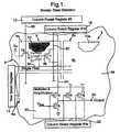
- a sensor 2such as a chemical sensor, comprises an array of sensor cells 4 a, 4 b . . . 4 n, arranged in rows 6 , 6 a . . . 6 n and columns 8 , 8 a . . . 8 n.
- Each sensor cell 4 aincludes a thin film transistor (TFT), T 1 , an electrode 10 , a further transistor T 6 and a reference capacitor Cr.
- the sensor 2also includes a column preset register 12 , a row select register 14 , and a column select register 16 , the function of which is described below.
- Multiplex and amplification circuit 20operating under the control of a second column select register 22 , is also provided for amplifying and multiplexing output signals from the sensor cells to provide an output signal from the sensor array on output line 24 .
- the electrode 10is shown as a plate electrode for receiving a finger tip, but, equally, the electrode 10 could comprise an electrode in solution.
- Each of the sensor cells of the arrayhas a circuit configured as the sensor cell 4 a shown in FIG. 1 .
- the sensor shown in FIG. 1operates in a steady state detection mode with the voltage on the gate electrode 26 of transistor T 1 being determined by the value of the capacitance arising on the electrode 10 (denoted by the capacitor symbol Cs in FIG. 1) resulting from the electrode 10 receiving a sample for identification, in combination with the value of the reference capacitor Cr.
- the sensor cells in a columnare preset by the application of a voltage from the column preset register 12 on preset line 28 .
- the transistor T 6 of each cellis turned ON and a bias voltage Vp is applied to the gate electrode 26 of transistor T 1 .
- the bias voltage Vpis provided so that transistor T 1 is set to a known operating point on its characteristic and is ready to switch from a non-conducting to a conducting condition. It also ensures that the voltage at the gate electrode 26 , when a subsequent pulse is applied thereto, as is described below, does not rise to a level which would cause too high a current to be passed by transistor T 1 , possibly destroying transistor T 1 .
- the row select register 14is used to provide row select pulses on line 30 to the node N via the reference capacitor Cr.
- the column select register 16is used to supply a column select pulse on line 32 .
- the row select and column select pulsesare only supplied to one row and one column at any point in time, enabling a single cell, such as the sensor cell 4 a in FIG. 1, to be selected. Assuming, for example, that a fingertip whose fingerprint is to be identified is being received by the sensor 4 a. A part of the fingertip will be received by the electrode 10 and an adjacent part of the fingertip will be received by electrode 10 a of the immediately adjacent sensor cell 4 b in column 8 a.
- the fingertip surfaceacts a co-operating electrode to the electrodes 10 and 10 a, and hence a value of capacitance, denoted as Cs in FIG. 1, can be read between the fingertip and each of the electrodes 10 and 10 a.
- the capacitances Cs and Crcreate in effect an AC potential divider and hence, when the sensor cell 4 a receives the row select pulse on line 30 , the magnitude of the voltage at node N will vary in dependence upon the value of the reference capacitance Cr and the value of the capacitance Cs arising from the fingertip on the electrode 10 .
- transistor T 1is biased almost to the point of conduction by the application of the voltage Vp to the gate electrode 26 .
- the magnitude of the voltage at node Pinitially at value Vp, will increase to a value determined by the relative values of the capacitances Cs and Cr.
- Cris a fixed reference value capacitor, the value of this voltage will be proportional to the value of capacitance Cs.
- the value of the output current from transistor T 1will also be proportional to the value of capacitance Cs.
- the tin film transistor T 1is, therefore, being controlled in dependence upon the value of the capacitance arising at the sample electrode 10 resulting from the receipt by the sample electrode of the sample to be identified, i.e. a portion of the fingerprint on the fingertip.
- the current on output line 34is fed to the multiplex and amplification circuit 20 .
- a transistor T 1is provided with a select signal from the second column select register 22 simultaneously with the column select signal on line 32 .
- a bias voltage V biasis provided to the gate electrode of transistor T 5 . In this manner the output current on line 34 can be amplified and multiplexed onto output 24 by appropriate selection of transistor T 1 . Likewise, the output current from other sensor cells can also be multiplexed onto output 24 .
- the sensor 2comprises fingerprint recognition apparatus
- a fingertip placed into contact with the sensorwill have ridges of the fingerprint pattern in contact with certain sample electrodes and troughs of the fingerprint pattern in contact with other sample electrodes.
- the value of capacitance Cs for the sensor cell 4 awill differ from the value of capacitance Cs for the sensor cell 4 b.
- the sensor 4may comprise a 200 ⁇ 300 sensor cell array.
- the sensor cells of the arraycan be sequentially scanned and the multiplexed output signals of the sensor cells appearing on output 24 can be fed to a store.
- a comparatormay compare the stored values for the samples with reference values and, as a result of such comparison, the fingerprint may be identified.
- the output signals on output 24may also be fed to a display for displaying an image of the fingerprint as sensed by the sensor 2 .
- the multiplex and amplification circuit 20is fabricated integrally with the sensor 2 , in which case the transistors of the circuit, of which transistors T 1 to T 5 are shown, may also comprise TFT's on a common substrate 36 with the sensor 2 .
- the transistor T 6 for each sensor cellmay also comprise a TFT.
- the substrate 36may comprise any suitable support material but, advantageously, if all of the transistors of the sensor 2 are fabricated as TFT's, the substrate 36 may preferably comprise plastics material.
- the steady state detection sensor shown in FIG. 1has been described with reference to a fingerprint recognition apparatus, it may also be used as a biosensor to detect or recognise biomaterials in solution, such as DNA or antibodies.
- a number of electrodesare provided which receive the substance in solution. The values of capacitance arising from the substance can be compared with known reference values in order to identify the particular substance.
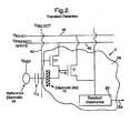
- FIG. 2shows an alternative embodiment for a sensor cell in accordance with the present invention.
- the sensor cell shown in FIG. 2operates in a ‘transient detection’ mode in which a time constant determined by, for example, the value of capacitance arising from an electrode receiving a DNA sample for identification, is used to identify the sample.
- a switching transistor T 7is coupled to the electrode 10 and a node P provided between the transistor T 7 and electrode 10 is coupled to the gate electrode of the thin film transistor T 1 .
- Select line 40 , write line 42 , and read line 44are provided for respectively providing select signal V select , preset signal V preset and read signal V read ,
- a multiplex and amplifier circuit 20is provided for providing an output signal on output 24 .
- the transient detection circuit shown in FIG. 2can also be used for fingerprint recognition, in a similar manner to that described with reference to FIG. 1 .
- reference electrode 46 of FIG. 2would be constituted by the surface of the fingertip and the voltage V ref of FIG. 2 would be provided by the charge occurring on the surface of the fingertip.
- the transistors T 1 and T 7which may both comprise TFT's, are in a non-conducting or OFF condition.
- the electrode 10is arranged as an electrode in a suitable reservoir into which is placed the DNA in solution.
- the DNAcan be immobilised and is therefore received by the electrode 10 and, as a result, a capacitance value C A arises between the sample electrode 10 and the reference electrode 46 .
- a preset cycleis initiated in which the switching transistor T 7 is switched from a non-conducting condition to a conducting condition by the application of the voltage V select to the gate electrode of transistor T 7 . Simultaneously, the preset voltage V preset is afforded to the source electrode of transistor T 7 and the read voltage V read is afforded to the source electrode of transistor T 1 .
- transistor T 7When transistor T 7 is switched ON, the voltage at node P rises to the level of preset voltage V preset and when the voltage at node P exceeds the threshold voltage of transistor T 1 , the transistor T 1 will switch ON with the current at the output of transistor T 1 being a function of the voltage at node P (the gate electrode of transistor T 1 ).
- a read cycleis then initiated by terminating the select voltage V select , causing transistor T 7 to switch back to a non-conducting or OFF condition.
- transistor T 7When transistor T 7 is switched OFF, the voltage on node P reduces by leaking away through transistor T 7 and the rate or the time constant for this leakage to occur depends on the value of capacitance C A , which is dependent upon the identity of the DNA sample received by the sample electrode 10 . As the voltage at the node P reduces in magnitude, there is a related decrease in the current at the output of thin film transistor T 1 , which is fed to the multiplex and amplification circuit 20 .
- transistor T 1switches OFF to further reduce the current fed to the multiplex and amplifier circuit 20 to that of a leakage current flowing through transistor T 1 .
- transistor T 7is used as a digital switching transistor whereas the transistor T 1 acts as an analogue voltage to current converter. Therefore, by monitoring the current at the output of transistor T 1 , which is dependent on the value of capacitance C A , the identity of the sample received by the electrode 10 can be determined.
- pairs of such sensor cellsmay be provided, one cell of a pair acting as the sample cell and the second of the pair acting as a reference cell in which no reaction has occurred.
- the chemical or biomaterials to be identifiedmust first be written into the cells and onto the reference electrodes. This can be regarded as a write phase for the cells and preferably occurs when the devices are fabricated.
- Inkjet headsmay conveniently be used to deposit the chemical or biomaterials and deposition onto the electrodes may be assisted by electrodeposition in which a charge is applied to the electrode so as to attract the material being deposited to its desired deposition site.
- FIG. 3shows an embodiment of a semiconductor structure which may be used to provide the thin film transistor T 1 , the electrode 10 , and the reference capacitor Cr.
- the TFT structure of FIG. 3comprises a layer of polysilicon 48 supported by the substrate 36 , which preferably is of plastics or soda glass material.
- the gate electrode 26is formed over the polysilicon layer 48 , separated from the polysilicon layer by an insulating layer 50 of silicon dioxide. Passivation layers 52 , 54 overlie the gate electrode 26 .
- the insulating layer 50 and the gate electrode 26are arranged to extend beyond the region of the polysilicon layer 48 to overlie a buried region 56 of metal or doped polysilicon formed on the substrate 36 .
- the passivation layers 52 , 54are provided with a well extending down to expose the gate electrode 26 in an area overlying the buried region 56 .
- the electrode 10which may comprise gold, silver or platinum, is formed in the well extending down into contact with the gate electrode 26 .
- the reference capacitoris provided between the buried region 56 and the gate electrode 26 .
- the reference capacitoris shown in phantom in FIG. 3 .
- the electrode 10can be positioned so that it is offset from the TFT without conflicting with the need to achieve maximum packing density on the expensive silicon substrate material.
- the electrode 10is therefore arranged so that it does not overlie the gate regions of the TFT.
- the electrode 10can be of enlarged size to improve device sensitivity but also the encapsulation required to isolate the TFT from the wet environment occurring at the electrode can be fabricated more easily and more reliably because there is no requirement to achieve a high packing density of devices on an expensive substrate.
- the structureprovides a compact arrangement incorporating the thin film transistor T 1 , the electrode 10 , and the reference capacitor Cr.
- the structurecan be incorporated into the steady state detection sensor cell shown in FIG. 1 .
- the value of capacitance C s arising between the electrode 10 and the sampleshown diagrammatically in FIG. 3, forms in combination with the integral reference capacitor Cr, the capacitance divider circuit described with reference to FIG. 1, which controls the operation of the TFT.
- the buried region 56can be omitted.
- FIG. 4illustrates an alternative circuit for a sensor cell which compensates for this variation and provides a comparable output from the TNT's across a large area substrate.
- the thin film transistor T 1is coupled via a switch S to either a constant current supply I Source or an output line.
- An additional transistor T 8which operates as a switching transistor, is connected between the gate and drain electrodes of thin film transistor T 1 , and the reference capacitor Cr is connected between the gate and source electrodes of transistor T 1 .
- the electrode for receiving the sample to be identified(not shown in FIG. 4) is also coupled to the gate electrode of transistor T 1 .
- the sample capacitance Csforms, therefore, a capacitance divider with the reference capacitor Cr, in a similar manner to that described with reference to FIG. 1 .
- transistor T 8When transistor T 8 is turned ON, the gate to source voltage V GS and drain to source voltage V DS for transistor T 1 will be equal. Under such conditions, the operational characteristic for transistor T 1 is simplified, as shown in FIG. 5 . With switch S in position “1”, the current from the constant current source I Source is pulled through transistor T 1 , which results in a voltage drop VD DSref across transistor T 1 . Because transistor T 8 is ON, (and hence G GS is equal to V DS for transistor T 1 ), the voltage drop V DSref appearing across transistor T 1 is stored in the reference capacitor Cr.
- Threshold variation in thin film transistor T 1may result in a shift in the simplified operational characteristic curve (when V GS is equal to V DS ) for transistor T 1 , as shown in FIG. 6 .
- the value of the current flowing through transistor T 1is constant as it is being supplied from the constant current source, I Source . Any threshold variation will therefore result in a change in the voltage drop V DSref occurring between the source and drain electrodes of transistor T 1 .
- the voltage V DSrefis stored in the reference capacitor Cr and, therefore, the voltage V GS between the gate and source electrodes of transistor T 1 is precharged to this value. In this way, transistor T 1 is preset to a known point on its characteristic.
- the current I out on the output linewill be equal to the current from the constant current supply I Source , as it is governed by the voltage at node P, which in turn is governed by the voltage stored on the reference capacitor Cr. If voltage source V ref is now pulsed, the voltage at node P increases and pulses in sympathy with the voltage V ref . The current I out at the output line will also pulse in sympathy with the increase in the voltage at the node P.
- the reference capacitor Cr and the capacitance Csform a capacitive divider and, hence, the increase in the voltage at node P when the voltage source V ref is pulsed will be determined by the relative capacitance values of Cr and Cs.
- the increase in the output current I out from its initial value equal to the current from the constant current supply I Sourcecan be measured to quantify the value of capacitance Cs, which is indicative of the sample received by the sample electrode.
- the switch Smay be provided by solid state switching means, such as thin film transistors on the substrate 36 .
- FIG. 7illustrates a further embodiment of the present invention where the sensor can be used as a pH sensor.
- the structure shown in FIG. 7is very similar to the structure shown in FIG. 3, so wherever possible like reference numerals have been used to indicate like parts of the structure.
- a well 58is provided in the passivation layer 52 to expose the gate electrode 26 .
- the passivation layer 54is provided extending as a continuous layer over the passivation layer 52 and the gate electrode 26 in the well 58 to provide a relatively thin layer of passivation material 60 overlying the gate electrode.
- the layer 60is very thin this charge transfers to the gate electrode 60 and provides therefore a voltage which controls the operation of the TFT transistor constituted by gate electrode 26 , polysilicon region 48 and silicon dioxide layer 50 .
- the charge created in the layer 60 by adsorption of the ions onto the surface 62is related to the pH of the solution deposited into the well 58 . Hence, by monitoring the output from the TFT the substance in solution can be identified.
- the sensor cellshave been described with reference to detection of chemical or biomaterials in liquid form. However, it should also be realised that the sensor cells may be used to analyse fluids other than liquids, such as gases.
- the present inventionhas been described with reference to one sensor cell being used to analyse a particular chemical or biomaterial sample.
- the matrix of sensor cells making up the sensormay be provided with several sensor cells, each having a particular DNA string written onto the reference electrode. If such cells are arranged in spaced relationship across the array, the output signals from these sensor cells having a common reference material, such as a DNA string, written onto the reference electrode may be averaged by appropriate circuitry so as to provide enhanced accuracy of analysis.
- the analysis circuitrymay also be fabricated on the substrate using TPT's. Therefore, in essence, the sensor may be provided with a number of ‘duplicate’ sensor cells, each arranged to identify the common DNA string. This is made possible through the use of TFT's because a very large number of sensor cells can be incorporated into a very large area array.
Landscapes
- Chemical & Material Sciences (AREA)
- Engineering & Computer Science (AREA)
- Microelectronics & Electronic Packaging (AREA)
- Health & Medical Sciences (AREA)
- Life Sciences & Earth Sciences (AREA)
- Electrochemistry (AREA)
- Molecular Biology (AREA)
- Chemical Kinetics & Catalysis (AREA)
- Computer Hardware Design (AREA)
- Physics & Mathematics (AREA)
- Analytical Chemistry (AREA)
- Biochemistry (AREA)
- General Health & Medical Sciences (AREA)
- General Physics & Mathematics (AREA)
- Immunology (AREA)
- Pathology (AREA)
- Thin Film Transistor (AREA)
- Investigating Or Analyzing Materials By The Use Of Electric Means (AREA)
Abstract
Description
Claims (49)
Applications Claiming Priority (3)
| Application Number | Priority Date | Filing Date | Title |
|---|---|---|---|
| GB0031716 | 2000-12-22 | ||
| GB0031716AGB2370410A (en) | 2000-12-22 | 2000-12-22 | Thin film transistor sensor |
| GB0031716.4 | 2000-12-22 |
Publications (2)
| Publication Number | Publication Date |
|---|---|
| US20020117694A1 US20020117694A1 (en) | 2002-08-29 |
| US6657269B2true US6657269B2 (en) | 2003-12-02 |
Family
ID=9905943
Family Applications (1)
| Application Number | Title | Priority Date | Filing Date |
|---|---|---|---|
| US10/022,232Expired - LifetimeUS6657269B2 (en) | 2000-12-22 | 2001-12-20 | Sensor cell |
Country Status (5)
| Country | Link |
|---|---|
| US (1) | US6657269B2 (en) |
| EP (1) | EP1217364B1 (en) |
| JP (1) | JP3969702B2 (en) |
| DE (1) | DE60133262T2 (en) |
| GB (1) | GB2370410A (en) |
Cited By (54)
| Publication number | Priority date | Publication date | Assignee | Title |
|---|---|---|---|---|
| US20030222659A1 (en)* | 2002-03-04 | 2003-12-04 | Seiko Epson Corporation | Electrostatic capacitance detection device |
| US20040239342A1 (en)* | 2003-04-17 | 2004-12-02 | Seiko Epson Corporation | Electrostatic capacitance detecting device |
| US20050077911A1 (en)* | 2003-08-29 | 2005-04-14 | Seiko Epson Corporation | Electrostatic capacitance detection device |
| US20050078856A1 (en)* | 2003-08-29 | 2005-04-14 | Seiko Epson Corporation | Electrostatic capacitance detection device |
| US20060076963A1 (en)* | 2004-10-12 | 2006-04-13 | Seiko Epson Corporation | Electrostatic capacitance detection device |
| US20060097735A1 (en)* | 2004-11-10 | 2006-05-11 | Seiko Epson Corporation | Electrostatic capacitance detection device |
| US20070029583A1 (en)* | 2002-09-25 | 2007-02-08 | Thomas Danielle A | Organic semiconductor sensor device |
| US20070247170A1 (en)* | 2004-06-09 | 2007-10-25 | Massimo Barbaro | Field-Effect Device for the Detection of Small Quantities of Electric Charge, Such as Those Generated in Bio-Molecular Process, Bound in the Vicinity of the Surface |
| US20070285900A1 (en)* | 2006-06-09 | 2007-12-13 | Chia-Chun Cheng | Cooling device for interface card |
| US20080087542A1 (en)* | 2002-02-12 | 2008-04-17 | Seiko Epson Corporation | Capacitance sensor with asynchronous ring oscillator circuit |
| US20080230859A1 (en)* | 2006-04-20 | 2008-09-25 | Mona Zaghloul | Saw devices, processes for making them, and methods of use |
| US20080265985A1 (en)* | 2004-07-13 | 2008-10-30 | Dna Electronics Ltd. | Signal Processing Circuit Comprising Ion Sensitive Field Effect Transistor and Method of Monitoring a Property of a Fluid |
| US20090114798A1 (en)* | 2007-04-20 | 2009-05-07 | Onur Tigli | Circular Surface Acoustic Wave (SAW) Devices, Processes for Making Them, and Methods of Use |
| US20090124513A1 (en)* | 2007-04-20 | 2009-05-14 | Patricia Berg | Multiplex Biosensor |
| US20100007444A1 (en)* | 2006-04-20 | 2010-01-14 | Anis Nurashikin Nordin | GHz Surface Acoustic Resonators in RF-CMOS |
| US20100097764A1 (en)* | 2006-11-30 | 2010-04-22 | Kabushiki Kaisha Toshiba | Electronic device |
| US20100246133A1 (en)* | 2009-03-31 | 2010-09-30 | Apple Inc. | Method and apparatus for distributing a thermal interface material |
| US20100284290A1 (en)* | 2009-04-09 | 2010-11-11 | Aegis Mobility, Inc. | Context based data mediation |
| US8552771B1 (en) | 2012-05-29 | 2013-10-08 | Life Technologies Corporation | System for reducing noise in a chemical sensor array |
| US8692298B2 (en) | 2006-12-14 | 2014-04-08 | Life Technologies Corporation | Chemical sensor array having multiple sensors per well |
| US8731847B2 (en) | 2010-06-30 | 2014-05-20 | Life Technologies Corporation | Array configuration and readout scheme |
| US8742472B2 (en) | 2006-12-14 | 2014-06-03 | Life Technologies Corporation | Chemically sensitive sensors with sample and hold capacitors |
| US8766651B2 (en) | 2012-05-22 | 2014-07-01 | Silicon Display Technology | Capacitive fingerprint sensor |
| US8841217B1 (en) | 2013-03-13 | 2014-09-23 | Life Technologies Corporation | Chemical sensor with protruded sensor surface |
| US8912005B1 (en) | 2010-09-24 | 2014-12-16 | Life Technologies Corporation | Method and system for delta double sampling |
| US8912580B2 (en) | 2009-05-29 | 2014-12-16 | Life Technologies Corporation | Active chemically-sensitive sensors with in-sensor current sources |
| US8962366B2 (en) | 2013-01-28 | 2015-02-24 | Life Technologies Corporation | Self-aligned well structures for low-noise chemical sensors |
| US8960004B2 (en) | 2010-09-29 | 2015-02-24 | The George Washington University | Synchronous one-pole surface acoustic wave resonator |
| US8963216B2 (en) | 2013-03-13 | 2015-02-24 | Life Technologies Corporation | Chemical sensor with sidewall spacer sensor surface |
| US9116117B2 (en) | 2013-03-15 | 2015-08-25 | Life Technologies Corporation | Chemical sensor with sidewall sensor surface |
| US9128044B2 (en) | 2013-03-15 | 2015-09-08 | Life Technologies Corporation | Chemical sensors with consistent sensor surface areas |
| US9194000B2 (en) | 2008-06-25 | 2015-11-24 | Life Technologies Corporation | Methods and apparatus for measuring analytes using large scale FET arrays |
| US9239313B2 (en) | 2010-06-30 | 2016-01-19 | Life Technologies Corporation | Ion-sensing charge-accumulation circuits and methods |
| US9404920B2 (en) | 2006-12-14 | 2016-08-02 | Life Technologies Corporation | Methods and apparatus for detecting molecular interactions using FET arrays |
| US20170006245A1 (en)* | 2015-06-30 | 2017-01-05 | Synaptics Incorporated | Active matrix capacitive fingerprint sensor for display integration based on charge sensing by a 2-tft pixel architecture |
| US9671363B2 (en) | 2013-03-15 | 2017-06-06 | Life Technologies Corporation | Chemical sensor with consistent sensor surface areas |
| US9792516B2 (en) | 2016-01-26 | 2017-10-17 | Next Biometrics Group Asa | Flexible card with fingerprint sensor |
| US9841398B2 (en) | 2013-01-08 | 2017-12-12 | Life Technologies Corporation | Methods for manufacturing well structures for low-noise chemical sensors |
| US9880688B2 (en) | 2015-08-05 | 2018-01-30 | Synaptics Incorporated | Active matrix capacitive sensor for common-mode cancellation |
| US9927393B2 (en) | 2009-05-29 | 2018-03-27 | Life Technologies Corporation | Methods and apparatus for measuring analytes |
| WO2018067136A1 (en)* | 2016-10-05 | 2018-04-12 | Hewlett-Packard Development Company, L.P. | Insulated sensors |
| US9944981B2 (en) | 2008-10-22 | 2018-04-17 | Life Technologies Corporation | Methods and apparatus for measuring analytes |
| US9946375B2 (en) | 2015-06-30 | 2018-04-17 | Synaptics Incorporated | Active matrix capacitive fingerprint sensor with 2-TFT pixel architecture for display integration |
| US9958414B2 (en) | 2010-09-15 | 2018-05-01 | Life Technologies Corporation | Apparatus for measuring analytes including chemical sensor array |
| US9958993B2 (en) | 2015-06-30 | 2018-05-01 | Synaptics Incorporated | Active matrix capacitive fingerprint sensor with 1-TFT pixel architecture for display integration |
| US9960253B2 (en) | 2010-07-03 | 2018-05-01 | Life Technologies Corporation | Chemically sensitive sensor with lightly doped drains |
| US10077472B2 (en) | 2014-12-18 | 2018-09-18 | Life Technologies Corporation | High data rate integrated circuit with power management |
| US10216972B2 (en) | 2017-01-13 | 2019-02-26 | Synaptics Incorporated | Pixel architecture and driving scheme for biometric sensing |
| US10379079B2 (en) | 2014-12-18 | 2019-08-13 | Life Technologies Corporation | Methods and apparatus for measuring analytes using large scale FET arrays |
| US10430633B2 (en) | 2017-01-13 | 2019-10-01 | Synaptics Incorporated | Pixel architecture and driving scheme for biometric sensing |
| US10458942B2 (en) | 2013-06-10 | 2019-10-29 | Life Technologies Corporation | Chemical sensor array having multiple sensors per well |
| US10605767B2 (en) | 2014-12-18 | 2020-03-31 | Life Technologies Corporation | High data rate integrated circuit with transmitter configuration |
| US11339430B2 (en) | 2007-07-10 | 2022-05-24 | Life Technologies Corporation | Methods and apparatus for measuring analytes using large scale FET arrays |
| US11631271B2 (en)* | 2017-11-17 | 2023-04-18 | Samsung Display Co., Ltd. | Fingerprint sensor and display device including the same |
Families Citing this family (41)
| Publication number | Priority date | Publication date | Assignee | Title |
|---|---|---|---|---|
| JP2003282791A (en)* | 2002-03-20 | 2003-10-03 | Fujitsu Ltd | Semiconductor device with built-in contact sensor and method of manufacturing the same |
| TW583592B (en)* | 2002-04-03 | 2004-04-11 | Lightuning Tech Inc | Capacitive fingerprint sensor |
| JP4399211B2 (en)* | 2002-12-21 | 2010-01-13 | 株式会社ハイニックスセミコンダクター | Biosensor |
| CN100392861C (en)* | 2003-01-08 | 2008-06-04 | 株式会社半导体能源研究所 | Semiconductor device and manufacturing method thereof |
| JP3775601B2 (en) | 2003-04-17 | 2006-05-17 | セイコーエプソン株式会社 | Capacitance detection device and driving method thereof, fingerprint sensor, and biometric authentication device |
| TWI253174B (en)* | 2003-05-09 | 2006-04-11 | Au Optronics Corp | Ion sensitive field effect transistor and fabrication method of the same |
| GB0322010D0 (en)* | 2003-09-19 | 2003-10-22 | Univ Cambridge Tech | Detection of molecular interactions using field effect transistors |
| DE102004023855B4 (en)* | 2004-05-13 | 2006-11-30 | Infineon Technologies Ag | Circuit arrangement |
| US8536661B1 (en) | 2004-06-25 | 2013-09-17 | University Of Hawaii | Biosensor chip sensor protection methods |
| TWI258173B (en)* | 2004-10-08 | 2006-07-11 | Ind Tech Res Inst | Polysilicon thin-film ion sensitive FET device and fabrication method thereof |
| WO2007008246A2 (en) | 2004-11-12 | 2007-01-18 | The Board Of Trustees Of The Leland Stanford Junior University | Charge perturbation detection system for dna and other molecules |
| JP4637914B2 (en)* | 2004-11-26 | 2011-02-23 | ミクロナス ゲーエムベーハー | Electrical components |
| US8323570B2 (en)* | 2006-03-21 | 2012-12-04 | Koninklijke Philips Electronics N.V. | Microelectronic sensor device with sensor array |
| KR100773548B1 (en)* | 2006-03-31 | 2007-11-07 | 삼성전자주식회사 | Method and apparatus for simultaneously detecting the size and concentration of ionic material |
| US8129978B2 (en) | 2006-07-13 | 2012-03-06 | National University Corporation Nagoya University | Material detector |
| WO2008044779A1 (en)* | 2006-10-06 | 2008-04-17 | Sharp Kabushiki Kaisha | Micro-pixelated fluid-assay structure, micro-pixelated fluid-assay precursor structure, and making method and performing method thereof |
| KR101176547B1 (en) | 2006-12-20 | 2012-08-24 | 리전츠 오브 더 유니버스티 오브 미네소타 | Apparatus and method of detecting ionic materials with reduced noise |
| WO2008132656A2 (en)* | 2007-04-27 | 2008-11-06 | Nxp B.V. | A biosensor chip and a method of manufacturing the same |
| JP4927777B2 (en)* | 2008-04-21 | 2012-05-09 | 日本電信電話株式会社 | Charge detector and charge detection method |
| US9401431B2 (en)* | 2009-04-21 | 2016-07-26 | Cbrite Inc. | Double self-aligned metal oxide TFT |
| US8574835B2 (en) | 2009-05-29 | 2013-11-05 | Life Technologies Corporation | Scaffolded nucleic acid polymer particles and methods of making and using |
| US8673627B2 (en) | 2009-05-29 | 2014-03-18 | Life Technologies Corporation | Apparatus and methods for performing electrochemical reactions |
| US20120261274A1 (en) | 2009-05-29 | 2012-10-18 | Life Technologies Corporation | Methods and apparatus for measuring analytes |
| JPWO2011152209A1 (en)* | 2010-06-03 | 2013-07-25 | シャープ株式会社 | Ion sensor and display device |
| TWI539172B (en) | 2010-06-30 | 2016-06-21 | 生命技術公司 | Methods and apparatus for testing isfet arrays |
| US11307166B2 (en) | 2010-07-01 | 2022-04-19 | Life Technologies Corporation | Column ADC |
| JP5472013B2 (en)* | 2010-09-30 | 2014-04-16 | 大日本印刷株式会社 | Transistor type sensor |
| US9970984B2 (en) | 2011-12-01 | 2018-05-15 | Life Technologies Corporation | Method and apparatus for identifying defects in a chemical sensor array |
| US8747748B2 (en) | 2012-01-19 | 2014-06-10 | Life Technologies Corporation | Chemical sensor with conductive cup-shaped sensor surface |
| US8821798B2 (en) | 2012-01-19 | 2014-09-02 | Life Technologies Corporation | Titanium nitride as sensing layer for microwell structure |
| US9080968B2 (en) | 2013-01-04 | 2015-07-14 | Life Technologies Corporation | Methods and systems for point of use removal of sacrificial material |
| US20140266262A1 (en)* | 2013-03-14 | 2014-09-18 | Perkinelmer Holdings, Inc. | High resolution fingerprint imaging device |
| JP6671274B2 (en) | 2013-03-15 | 2020-03-25 | ライフ テクノロジーズ コーポレーション | Chemical device with thin conductive element |
| US20140336063A1 (en) | 2013-05-09 | 2014-11-13 | Life Technologies Corporation | Windowed Sequencing |
| WO2015007369A1 (en)* | 2013-07-19 | 2015-01-22 | Merck Patent Gmbh | Biosensor array |
| JP2015210233A (en)* | 2014-04-30 | 2015-11-24 | 国立大学法人名古屋大学 | Massively parallel biomolecule detection method and apparatus |
| US10618301B2 (en)* | 2015-07-24 | 2020-04-14 | Hewlett-Packard Development Company, L.P. | Semiconductor device including capacitive sensor and ion-sensitive transistor for determining level and ion-concentration of fluid |
| JP6656507B2 (en)* | 2015-09-18 | 2020-03-04 | Tianma Japan株式会社 | Biosensor and detection device |
| CN108600662B (en)* | 2018-07-24 | 2023-09-26 | 思特威(上海)电子科技股份有限公司 | Image sensor pixel circuit and imaging system |
| US12299098B2 (en) | 2019-06-05 | 2025-05-13 | Touch Biometrix Limited | Pointing device with biometric skin-contact sensor, and corresponding method |
| WO2023157711A1 (en)* | 2022-02-15 | 2023-08-24 | 国立大学法人広島大学 | Inspection chip, reaction detection device, and reaction detection method |
Citations (10)
| Publication number | Priority date | Publication date | Assignee | Title |
|---|---|---|---|---|
| WO1989009932A1 (en) | 1988-04-14 | 1989-10-19 | Terumo Kabushiki Kaisha | Ion sensor |
| US4968400A (en)* | 1986-11-20 | 1990-11-06 | Terumo Kabushiki Kaisha | Enzyme sensor |
| EP0751392A2 (en) | 1995-06-28 | 1997-01-02 | Motorola, Inc. | Biosensor or chemical sensor with indicator film |
| WO1997039145A1 (en) | 1996-04-17 | 1997-10-23 | Motorola Inc. | Transistor-based molecular detection apparatus and method |
| US5827482A (en) | 1996-08-20 | 1998-10-27 | Motorola Corporation | Transistor-based apparatus and method for molecular detection and field enhancement |
| EP0908725A1 (en) | 1997-09-30 | 1999-04-14 | Seiko Epson Corporation | Manufacture of a microsensor device |
| US6111280A (en)* | 1997-01-15 | 2000-08-29 | University Of Warwick | Gas-sensing semiconductor devices |
| EP1041356A1 (en) | 1999-03-31 | 2000-10-04 | Mitsubishi Denki Kabushiki Kaisha | Uneveness detecting sensor, fingerprint ID system and personal ID system |
| US6200444B1 (en)* | 1996-03-29 | 2001-03-13 | Institut Fuer Chemo Und Biosensorik Muenster E.V. | Cation-selective sensor |
| US6411727B1 (en)* | 1998-02-05 | 2002-06-25 | Koninklijke Philips Electronics N.V. | Fingerprint sensing devices and systems incorporating such |
Family Cites Families (10)
| Publication number | Priority date | Publication date | Assignee | Title |
|---|---|---|---|---|
| JPH03125252U (en)* | 1990-03-31 | 1991-12-18 | ||
| JP2514280B2 (en)* | 1990-07-03 | 1996-07-10 | 株式会社日立製作所 | Integrated ion sensor |
| GB9615278D0 (en)* | 1996-07-20 | 1996-09-04 | Philips Electronics Nv | Capacitive sensing array device |
| EP0969477B1 (en)* | 1998-07-02 | 2006-09-27 | Nippon Telegraph and Telephone Corporation | Small capacitance change detection device |
| JP3356401B2 (en)* | 1998-07-02 | 2002-12-16 | 日本電信電話株式会社 | Surface shape recognition sensor |
| JP4320069B2 (en)* | 1998-09-28 | 2009-08-26 | セイコーエプソン株式会社 | How to create a sensor device |
| JP2000213908A (en)* | 1998-11-16 | 2000-08-04 | Sony Corp | Electrostatic capacity detecting device, its detecting method and fingerprint collating device |
| JP2000166900A (en)* | 1998-12-03 | 2000-06-20 | Sony Corp | Fingerprint sensor and fingerprint data generation method thereof |
| JP2000279397A (en)* | 1999-03-31 | 2000-10-10 | Mitsubishi Electric Corp | Unevenness detection sensor, unevenness detection device, fingerprint collation device and personal identification device |
| JP2001311752A (en)* | 1999-10-26 | 2001-11-09 | Citizen Watch Co Ltd | Electrostatic capacity detecting device |
- 2000
- 2000-12-22GBGB0031716Apatent/GB2370410A/ennot_activeWithdrawn
- 2001
- 2001-12-20EPEP01310664Apatent/EP1217364B1/ennot_activeExpired - Lifetime
- 2001-12-20DEDE60133262Tpatent/DE60133262T2/ennot_activeExpired - Lifetime
- 2001-12-20USUS10/022,232patent/US6657269B2/ennot_activeExpired - Lifetime
- 2001-12-21JPJP2001389680Apatent/JP3969702B2/ennot_activeExpired - Lifetime
Patent Citations (11)
| Publication number | Priority date | Publication date | Assignee | Title |
|---|---|---|---|---|
| US4968400A (en)* | 1986-11-20 | 1990-11-06 | Terumo Kabushiki Kaisha | Enzyme sensor |
| WO1989009932A1 (en) | 1988-04-14 | 1989-10-19 | Terumo Kabushiki Kaisha | Ion sensor |
| EP0751392A2 (en) | 1995-06-28 | 1997-01-02 | Motorola, Inc. | Biosensor or chemical sensor with indicator film |
| US5719033A (en)* | 1995-06-28 | 1998-02-17 | Motorola, Inc. | Thin film transistor bio/chemical sensor |
| US6200444B1 (en)* | 1996-03-29 | 2001-03-13 | Institut Fuer Chemo Und Biosensorik Muenster E.V. | Cation-selective sensor |
| WO1997039145A1 (en) | 1996-04-17 | 1997-10-23 | Motorola Inc. | Transistor-based molecular detection apparatus and method |
| US5827482A (en) | 1996-08-20 | 1998-10-27 | Motorola Corporation | Transistor-based apparatus and method for molecular detection and field enhancement |
| US6111280A (en)* | 1997-01-15 | 2000-08-29 | University Of Warwick | Gas-sensing semiconductor devices |
| EP0908725A1 (en) | 1997-09-30 | 1999-04-14 | Seiko Epson Corporation | Manufacture of a microsensor device |
| US6411727B1 (en)* | 1998-02-05 | 2002-06-25 | Koninklijke Philips Electronics N.V. | Fingerprint sensing devices and systems incorporating such |
| EP1041356A1 (en) | 1999-03-31 | 2000-10-04 | Mitsubishi Denki Kabushiki Kaisha | Uneveness detecting sensor, fingerprint ID system and personal ID system |
Cited By (119)
| Publication number | Priority date | Publication date | Assignee | Title |
|---|---|---|---|---|
| US20080087542A1 (en)* | 2002-02-12 | 2008-04-17 | Seiko Epson Corporation | Capacitance sensor with asynchronous ring oscillator circuit |
| US7127089B2 (en)* | 2002-03-04 | 2006-10-24 | Seiko Epson Corporation | Electrostatic capacitance detection device |
| US20030222659A1 (en)* | 2002-03-04 | 2003-12-04 | Seiko Epson Corporation | Electrostatic capacitance detection device |
| US8569809B2 (en)* | 2002-09-25 | 2013-10-29 | Stmicroelectronics, Inc. | Organic semiconductor sensor device |
| US20070029583A1 (en)* | 2002-09-25 | 2007-02-08 | Thomas Danielle A | Organic semiconductor sensor device |
| US20040239342A1 (en)* | 2003-04-17 | 2004-12-02 | Seiko Epson Corporation | Electrostatic capacitance detecting device |
| US7205778B2 (en) | 2003-04-17 | 2007-04-17 | Seiko Epson Corporation | Electrostatic capacitance detecting device |
| US20060125490A1 (en)* | 2003-04-17 | 2006-06-15 | Seiko Epson Corporation | Electrostatic capacitance detecting device |
| US7078917B2 (en)* | 2003-04-17 | 2006-07-18 | Seiko Epson Corporation | Electrostatic capacitance detecting device |
| US7081765B2 (en)* | 2003-08-29 | 2006-07-25 | Seiko Epson Corporation | Electrostatic capacitance detection device |
| US7126350B2 (en)* | 2003-08-29 | 2006-10-24 | Seiko Epson Corporation | Electrostatic capacitance detection device |
| US20050078856A1 (en)* | 2003-08-29 | 2005-04-14 | Seiko Epson Corporation | Electrostatic capacitance detection device |
| US20050077911A1 (en)* | 2003-08-29 | 2005-04-14 | Seiko Epson Corporation | Electrostatic capacitance detection device |
| US7535232B2 (en)* | 2004-06-09 | 2009-05-19 | Consiglio Nazionale Delle Ricerche | Field-effect device for the detection of small quantities of electric charge, such as those generated in bio-molecular process, bound in the vicinity of the surface |
| US20070247170A1 (en)* | 2004-06-09 | 2007-10-25 | Massimo Barbaro | Field-Effect Device for the Detection of Small Quantities of Electric Charge, Such as Those Generated in Bio-Molecular Process, Bound in the Vicinity of the Surface |
| US7649358B2 (en)* | 2004-07-13 | 2010-01-19 | Dna Electronics Ltd. | Signal processing circuit comprising ion sensitive field effect transistor and method of monitoring a property of a fluid |
| US20080265985A1 (en)* | 2004-07-13 | 2008-10-30 | Dna Electronics Ltd. | Signal Processing Circuit Comprising Ion Sensitive Field Effect Transistor and Method of Monitoring a Property of a Fluid |
| CN100410621C (en)* | 2004-10-12 | 2008-08-13 | 精工爱普生株式会社 | Electrostatic capacitance detection device |
| US7208961B2 (en)* | 2004-10-12 | 2007-04-24 | Seiko Epson Corporation | Electrostatic capacitance detection device |
| US20060076963A1 (en)* | 2004-10-12 | 2006-04-13 | Seiko Epson Corporation | Electrostatic capacitance detection device |
| US7196528B2 (en)* | 2004-11-10 | 2007-03-27 | Seiko Epson Corporation | Electrostatic capacitance detection device |
| US20060097735A1 (en)* | 2004-11-10 | 2006-05-11 | Seiko Epson Corporation | Electrostatic capacitance detection device |
| US20080230859A1 (en)* | 2006-04-20 | 2008-09-25 | Mona Zaghloul | Saw devices, processes for making them, and methods of use |
| US8143681B2 (en) | 2006-04-20 | 2012-03-27 | The George Washington University | Saw devices, processes for making them, and methods of use |
| US20100007444A1 (en)* | 2006-04-20 | 2010-01-14 | Anis Nurashikin Nordin | GHz Surface Acoustic Resonators in RF-CMOS |
| US20070285900A1 (en)* | 2006-06-09 | 2007-12-13 | Chia-Chun Cheng | Cooling device for interface card |
| US7468885B2 (en)* | 2006-06-09 | 2008-12-23 | Cooler Master Co., Ltd. | Cooling device for interface card |
| US20100097764A1 (en)* | 2006-11-30 | 2010-04-22 | Kabushiki Kaisha Toshiba | Electronic device |
| US7830663B2 (en)* | 2006-11-30 | 2010-11-09 | Kabushiki Kaisha Toshiba | Electronic device |
| US10502708B2 (en) | 2006-12-14 | 2019-12-10 | Life Technologies Corporation | Chemically-sensitive sensor array calibration circuitry |
| US10633699B2 (en) | 2006-12-14 | 2020-04-28 | Life Technologies Corporation | Methods and apparatus for measuring analytes using large scale FET arrays |
| US12140560B2 (en) | 2006-12-14 | 2024-11-12 | Life Technologies Corporation | Methods and apparatus for measuring analytes using large scale FET arrays |
| US9269708B2 (en) | 2006-12-14 | 2016-02-23 | Life Technologies Corporation | Methods and apparatus for measuring analytes using large scale FET arrays |
| US9023189B2 (en) | 2006-12-14 | 2015-05-05 | Life Technologies Corporation | High density sensor array without wells |
| US9404920B2 (en) | 2006-12-14 | 2016-08-02 | Life Technologies Corporation | Methods and apparatus for detecting molecular interactions using FET arrays |
| US11435314B2 (en) | 2006-12-14 | 2022-09-06 | Life Technologies Corporation | Chemically-sensitive sensor array device |
| US11732297B2 (en)* | 2006-12-14 | 2023-08-22 | Life Technologies Corporation | Methods and apparatus for measuring analytes using large scale FET arrays |
| US9951382B2 (en) | 2006-12-14 | 2018-04-24 | Life Technologies Corporation | Methods and apparatus for measuring analytes using large scale FET arrays |
| US8692298B2 (en) | 2006-12-14 | 2014-04-08 | Life Technologies Corporation | Chemical sensor array having multiple sensors per well |
| US20220340965A1 (en)* | 2006-12-14 | 2022-10-27 | Life Technologies Corporation | Methods and Apparatus for Measuring Analytes Using Large Scale FET Arrays |
| US9989489B2 (en) | 2006-12-14 | 2018-06-05 | Life Technnologies Corporation | Methods for calibrating an array of chemically-sensitive sensors |
| US9134269B2 (en) | 2006-12-14 | 2015-09-15 | Life Technologies Corporation | Methods and apparatus for measuring analytes using large scale FET arrays |
| US8742472B2 (en) | 2006-12-14 | 2014-06-03 | Life Technologies Corporation | Chemically sensitive sensors with sample and hold capacitors |
| US12066399B2 (en) | 2006-12-14 | 2024-08-20 | Life Technologies Corporation | Methods and apparatus for measuring analytes using large scale FET arrays |
| US8766328B2 (en) | 2006-12-14 | 2014-07-01 | Life Technologies Corporation | Chemically-sensitive sample and hold sensors |
| US8890216B2 (en) | 2006-12-14 | 2014-11-18 | Life Technologies Corporation | Methods and apparatus for measuring analytes using large scale FET arrays |
| US10816506B2 (en) | 2006-12-14 | 2020-10-27 | Life Technologies Corporation | Method for measuring analytes using large scale chemfet arrays |
| US20090114798A1 (en)* | 2007-04-20 | 2009-05-07 | Onur Tigli | Circular Surface Acoustic Wave (SAW) Devices, Processes for Making Them, and Methods of Use |
| US20090124513A1 (en)* | 2007-04-20 | 2009-05-14 | Patricia Berg | Multiplex Biosensor |
| US8018010B2 (en) | 2007-04-20 | 2011-09-13 | The George Washington University | Circular surface acoustic wave (SAW) devices, processes for making them, and methods of use |
| US11339430B2 (en) | 2007-07-10 | 2022-05-24 | Life Technologies Corporation | Methods and apparatus for measuring analytes using large scale FET arrays |
| US9194000B2 (en) | 2008-06-25 | 2015-11-24 | Life Technologies Corporation | Methods and apparatus for measuring analytes using large scale FET arrays |
| US11137369B2 (en) | 2008-10-22 | 2021-10-05 | Life Technologies Corporation | Integrated sensor arrays for biological and chemical analysis |
| US9944981B2 (en) | 2008-10-22 | 2018-04-17 | Life Technologies Corporation | Methods and apparatus for measuring analytes |
| US12146853B2 (en) | 2008-10-22 | 2024-11-19 | Life Technologies Corporation | Methods and apparatus including array of reaction chambers over array of chemFET sensors for measuring analytes |
| US11448613B2 (en) | 2008-10-22 | 2022-09-20 | Life Technologies Corporation | ChemFET sensor array including overlying array of wells |
| US11874250B2 (en) | 2008-10-22 | 2024-01-16 | Life Technologies Corporation | Integrated sensor arrays for biological and chemical analysis |
| US20100246133A1 (en)* | 2009-03-31 | 2010-09-30 | Apple Inc. | Method and apparatus for distributing a thermal interface material |
| US7961469B2 (en)* | 2009-03-31 | 2011-06-14 | Apple Inc. | Method and apparatus for distributing a thermal interface material |
| US20110228482A1 (en)* | 2009-03-31 | 2011-09-22 | Apple Inc. | Method and apparatus for distributing a thermal interface material |
| US8564955B2 (en) | 2009-03-31 | 2013-10-22 | Apple Inc. | Coupling heat sink to integrated circuit chip with thermal interface material |
| US20100284290A1 (en)* | 2009-04-09 | 2010-11-11 | Aegis Mobility, Inc. | Context based data mediation |
| US9927393B2 (en) | 2009-05-29 | 2018-03-27 | Life Technologies Corporation | Methods and apparatus for measuring analytes |
| US8912580B2 (en) | 2009-05-29 | 2014-12-16 | Life Technologies Corporation | Active chemically-sensitive sensors with in-sensor current sources |
| US10718733B2 (en) | 2009-05-29 | 2020-07-21 | Life Technologies Corporation | Methods and apparatus for measuring analytes |
| US10809226B2 (en) | 2009-05-29 | 2020-10-20 | Life Technologies Corporation | Methods and apparatus for measuring analytes |
| US11692964B2 (en) | 2009-05-29 | 2023-07-04 | Life Technologies Corporation | Methods and apparatus for measuring analytes |
| US12038405B2 (en) | 2009-05-29 | 2024-07-16 | Life Technologies Corporation | Methods and apparatus for measuring analytes |
| US11768171B2 (en) | 2009-05-29 | 2023-09-26 | Life Technologies Corporation | Methods and apparatus for measuring analytes |
| US8983783B2 (en) | 2010-06-30 | 2015-03-17 | Life Technologies Corporation | Chemical detection device having multiple flow channels |
| US12038406B2 (en) | 2010-06-30 | 2024-07-16 | Life Technologies Corporation | Semiconductor-based chemical detection device |
| US8731847B2 (en) | 2010-06-30 | 2014-05-20 | Life Technologies Corporation | Array configuration and readout scheme |
| US8742471B2 (en) | 2010-06-30 | 2014-06-03 | Life Technologies Corporation | Chemical sensor array with leakage compensation circuit |
| US8741680B2 (en) | 2010-06-30 | 2014-06-03 | Life Technologies Corporation | Two-transistor pixel array |
| US10481123B2 (en) | 2010-06-30 | 2019-11-19 | Life Technologies Corporation | Ion-sensing charge-accumulation circuits and methods |
| US9239313B2 (en) | 2010-06-30 | 2016-01-19 | Life Technologies Corporation | Ion-sensing charge-accumulation circuits and methods |
| US9960253B2 (en) | 2010-07-03 | 2018-05-01 | Life Technologies Corporation | Chemically sensitive sensor with lightly doped drains |
| US12050195B2 (en) | 2010-09-15 | 2024-07-30 | Life Technologies Corporation | Methods and apparatus for measuring analytes using chemfet arrays |
| US9958414B2 (en) | 2010-09-15 | 2018-05-01 | Life Technologies Corporation | Apparatus for measuring analytes including chemical sensor array |
| US9110015B2 (en) | 2010-09-24 | 2015-08-18 | Life Technologies Corporation | Method and system for delta double sampling |
| US8912005B1 (en) | 2010-09-24 | 2014-12-16 | Life Technologies Corporation | Method and system for delta double sampling |
| US8960004B2 (en) | 2010-09-29 | 2015-02-24 | The George Washington University | Synchronous one-pole surface acoustic wave resonator |
| US8766651B2 (en) | 2012-05-22 | 2014-07-01 | Silicon Display Technology | Capacitive fingerprint sensor |
| US9270264B2 (en) | 2012-05-29 | 2016-02-23 | Life Technologies Corporation | System for reducing noise in a chemical sensor array |
| US8552771B1 (en) | 2012-05-29 | 2013-10-08 | Life Technologies Corporation | System for reducing noise in a chemical sensor array |
| US8786331B2 (en) | 2012-05-29 | 2014-07-22 | Life Technologies Corporation | System for reducing noise in a chemical sensor array |
| US9841398B2 (en) | 2013-01-08 | 2017-12-12 | Life Technologies Corporation | Methods for manufacturing well structures for low-noise chemical sensors |
| US10436742B2 (en) | 2013-01-08 | 2019-10-08 | Life Technologies Corporation | Methods for manufacturing well structures for low-noise chemical sensors |
| US8962366B2 (en) | 2013-01-28 | 2015-02-24 | Life Technologies Corporation | Self-aligned well structures for low-noise chemical sensors |
| US9995708B2 (en) | 2013-03-13 | 2018-06-12 | Life Technologies Corporation | Chemical sensor with sidewall spacer sensor surface |
| US8841217B1 (en) | 2013-03-13 | 2014-09-23 | Life Technologies Corporation | Chemical sensor with protruded sensor surface |
| US8963216B2 (en) | 2013-03-13 | 2015-02-24 | Life Technologies Corporation | Chemical sensor with sidewall spacer sensor surface |
| US9128044B2 (en) | 2013-03-15 | 2015-09-08 | Life Technologies Corporation | Chemical sensors with consistent sensor surface areas |
| US10422767B2 (en) | 2013-03-15 | 2019-09-24 | Life Technologies Corporation | Chemical sensor with consistent sensor surface areas |
| US9116117B2 (en) | 2013-03-15 | 2015-08-25 | Life Technologies Corporation | Chemical sensor with sidewall sensor surface |
| US9671363B2 (en) | 2013-03-15 | 2017-06-06 | Life Technologies Corporation | Chemical sensor with consistent sensor surface areas |
| US10816504B2 (en) | 2013-06-10 | 2020-10-27 | Life Technologies Corporation | Chemical sensor array having multiple sensors per well |
| US11774401B2 (en) | 2013-06-10 | 2023-10-03 | Life Technologies Corporation | Chemical sensor array having multiple sensors per well |
| US10458942B2 (en) | 2013-06-10 | 2019-10-29 | Life Technologies Corporation | Chemical sensor array having multiple sensors per well |
| US11499938B2 (en) | 2013-06-10 | 2022-11-15 | Life Technologies Corporation | Chemical sensor array having multiple sensors per well |
| US12196704B2 (en) | 2014-12-18 | 2025-01-14 | Life Technologies Corporation | High data rate integrated circuit with transmitter configuration |
| US10077472B2 (en) | 2014-12-18 | 2018-09-18 | Life Technologies Corporation | High data rate integrated circuit with power management |
| US10379079B2 (en) | 2014-12-18 | 2019-08-13 | Life Technologies Corporation | Methods and apparatus for measuring analytes using large scale FET arrays |
| US10767224B2 (en) | 2014-12-18 | 2020-09-08 | Life Technologies Corporation | High data rate integrated circuit with power management |
| US11536688B2 (en) | 2014-12-18 | 2022-12-27 | Life Technologies Corporation | High data rate integrated circuit with transmitter configuration |
| US10605767B2 (en) | 2014-12-18 | 2020-03-31 | Life Technologies Corporation | High data rate integrated circuit with transmitter configuration |
| US9958993B2 (en) | 2015-06-30 | 2018-05-01 | Synaptics Incorporated | Active matrix capacitive fingerprint sensor with 1-TFT pixel architecture for display integration |
| US9946375B2 (en) | 2015-06-30 | 2018-04-17 | Synaptics Incorporated | Active matrix capacitive fingerprint sensor with 2-TFT pixel architecture for display integration |
| US10325131B2 (en)* | 2015-06-30 | 2019-06-18 | Synaptics Incorporated | Active matrix capacitive fingerprint sensor for display integration based on charge sensing by a 2-TFT pixel architecture |
| US20170006245A1 (en)* | 2015-06-30 | 2017-01-05 | Synaptics Incorporated | Active matrix capacitive fingerprint sensor for display integration based on charge sensing by a 2-tft pixel architecture |
| US9880688B2 (en) | 2015-08-05 | 2018-01-30 | Synaptics Incorporated | Active matrix capacitive sensor for common-mode cancellation |
| US9792516B2 (en) | 2016-01-26 | 2017-10-17 | Next Biometrics Group Asa | Flexible card with fingerprint sensor |
| US10055664B2 (en) | 2016-01-26 | 2018-08-21 | Next Biometrics Group Asa | Flexible card with fingerprint sensor |
| WO2018067136A1 (en)* | 2016-10-05 | 2018-04-12 | Hewlett-Packard Development Company, L.P. | Insulated sensors |
| US10876986B2 (en) | 2016-10-05 | 2020-12-29 | Hewlett-Packard Development Company, L.P. | Insulated sensors |
| US10216972B2 (en) | 2017-01-13 | 2019-02-26 | Synaptics Incorporated | Pixel architecture and driving scheme for biometric sensing |
| US10430633B2 (en) | 2017-01-13 | 2019-10-01 | Synaptics Incorporated | Pixel architecture and driving scheme for biometric sensing |
| US11631271B2 (en)* | 2017-11-17 | 2023-04-18 | Samsung Display Co., Ltd. | Fingerprint sensor and display device including the same |
| US12216866B2 (en) | 2017-11-17 | 2025-02-04 | Samsung Display Co., Ltd. | Fingerprint sensor and display device including the same |
Also Published As
| Publication number | Publication date |
|---|---|
| DE60133262T2 (en) | 2009-04-16 |
| EP1217364A3 (en) | 2004-01-02 |
| US20020117694A1 (en) | 2002-08-29 |
| JP3969702B2 (en) | 2007-09-05 |
| JP2003004697A (en) | 2003-01-08 |
| DE60133262D1 (en) | 2008-04-30 |
| EP1217364A2 (en) | 2002-06-26 |
| GB2370410A (en) | 2002-06-26 |
| EP1217364B1 (en) | 2008-03-19 |
| GB0031716D0 (en) | 2001-02-07 |
Similar Documents
| Publication | Publication Date | Title |
|---|---|---|
| US6657269B2 (en) | Sensor cell | |
| US7049645B2 (en) | FET type sensor, ion density detecting method comprising this sensor, and base sequence detecting method | |
| US20080087542A1 (en) | Capacitance sensor with asynchronous ring oscillator circuit | |
| TWI303714B (en) | Nucleic acid detecting sensor, nucleic acid detecting chip, and nucleic acid detecting circuit | |
| US5583462A (en) | Method and apparatus for multiplexing devices having long thermal time constants | |
| US10571426B2 (en) | Bio-sensor pixel circuit with amplification | |
| US7884398B2 (en) | Floating gate field effect transistors for chemical and/or biological sensing | |
| KR101056385B1 (en) | Detection element | |
| US7616423B2 (en) | Electronic equipment, driving method thereof and method of driving electronic circuit | |
| EP0953152B1 (en) | Gas-sensing semiconductor devices | |
| US20120168826A1 (en) | One-transistor pixel array | |
| JP2006138846A (en) | Nucleic acid detection sensor, nucleic acid detection chip and nucleic acid detection apparatus | |
| Schöning et al. | A novel silicon-based sensor array with capacitive EIS structures | |
| WO2016111237A1 (en) | Target substance detection method using fet biosensor | |
| US20020033705A1 (en) | Method and apparatus for measuring hysteresis and drift values of an isfet using the hydrogenated amorphous silicon as a sensing film | |
| CN114624308B (en) | Ion sensing apparatus | |
| JP4941903B2 (en) | Electronic device, driving method thereof, and driving method of electronic circuit | |
| EP4332562A1 (en) | A mesfet biosensor and a biosensing kit | |
| Estrela et al. | Application of thin film transistors to label-free electrical biosensors |
Legal Events
| Date | Code | Title | Description |
|---|---|---|---|
| AS | Assignment | Owner name:SEIKO EPSON CORPORATION, JAPAN Free format text:ASSIGNMENT OF ASSIGNORS INTEREST;ASSIGNORS:MIGLIORATO, PIERO;BAVIDGE, NATHAN;LOWE, CHRISTOPHER;REEL/FRAME:014034/0762;SIGNING DATES FROM 20030731 TO 20030902 | |
| STCF | Information on status: patent grant | Free format text:PATENTED CASE | |
| AS | Assignment | Owner name:CAMBRIDGE UNIVERSITY TECHNICAL SERVICES LIMITED, G Free format text:ASSIGNMENT OF ASSIGNORS INTEREST;ASSIGNOR:SEIKO EPSON CORPORATION;REEL/FRAME:015596/0971 Effective date:20031230 Owner name:SEIKO EPSON CORPORATION, JAPAN Free format text:ASSIGNMENT OF ASSIGNORS INTEREST;ASSIGNOR:SEIKO EPSON CORPORATION;REEL/FRAME:015596/0971 Effective date:20031230 | |
| FEPP | Fee payment procedure | Free format text:PAYOR NUMBER ASSIGNED (ORIGINAL EVENT CODE: ASPN); ENTITY STATUS OF PATENT OWNER: LARGE ENTITY | |
| FPAY | Fee payment | Year of fee payment:4 | |
| FPAY | Fee payment | Year of fee payment:8 | |
| FPAY | Fee payment | Year of fee payment:12 |