US6657259B2 - Multiple-plane FinFET CMOS - Google Patents
Multiple-plane FinFET CMOSDownload PDFInfo
- Publication number
- US6657259B2 US6657259B2US10/011,846US1184601AUS6657259B2US 6657259 B2US6657259 B2US 6657259B2US 1184601 AUS1184601 AUS 1184601AUS 6657259 B2US6657259 B2US 6657259B2
- Authority
- US
- United States
- Prior art keywords
- crystal plane
- oriented
- plane
- sidewall
- crystal
- Prior art date
- Legal status (The legal status is an assumption and is not a legal conclusion. Google has not performed a legal analysis and makes no representation as to the accuracy of the status listed.)
- Expired - Lifetime
Links
Images


Classifications
- H—ELECTRICITY
- H10—SEMICONDUCTOR DEVICES; ELECTRIC SOLID-STATE DEVICES NOT OTHERWISE PROVIDED FOR
- H10D—INORGANIC ELECTRIC SEMICONDUCTOR DEVICES
- H10D30/00—Field-effect transistors [FET]
- H10D30/01—Manufacture or treatment
- H10D30/021—Manufacture or treatment of FETs having insulated gates [IGFET]
- H10D30/024—Manufacture or treatment of FETs having insulated gates [IGFET] of fin field-effect transistors [FinFET]
- H—ELECTRICITY
- H10—SEMICONDUCTOR DEVICES; ELECTRIC SOLID-STATE DEVICES NOT OTHERWISE PROVIDED FOR
- H10D—INORGANIC ELECTRIC SEMICONDUCTOR DEVICES
- H10D30/00—Field-effect transistors [FET]
- H10D30/60—Insulated-gate field-effect transistors [IGFET]
- H10D30/62—Fin field-effect transistors [FinFET]
- H—ELECTRICITY
- H10—SEMICONDUCTOR DEVICES; ELECTRIC SOLID-STATE DEVICES NOT OTHERWISE PROVIDED FOR
- H10D—INORGANIC ELECTRIC SEMICONDUCTOR DEVICES
- H10D62/00—Semiconductor bodies, or regions thereof, of devices having potential barriers
- H10D62/40—Crystalline structures
- H10D62/405—Orientations of crystalline planes
- H—ELECTRICITY
- H10—SEMICONDUCTOR DEVICES; ELECTRIC SOLID-STATE DEVICES NOT OTHERWISE PROVIDED FOR
- H10D—INORGANIC ELECTRIC SEMICONDUCTOR DEVICES
- H10D86/00—Integrated devices formed in or on insulating or conducting substrates, e.g. formed in silicon-on-insulator [SOI] substrates or on stainless steel or glass substrates
- H10D86/01—Manufacture or treatment
- H10D86/011—Manufacture or treatment comprising FinFETs
- H—ELECTRICITY
- H10—SEMICONDUCTOR DEVICES; ELECTRIC SOLID-STATE DEVICES NOT OTHERWISE PROVIDED FOR
- H10D—INORGANIC ELECTRIC SEMICONDUCTOR DEVICES
- H10D86/00—Integrated devices formed in or on insulating or conducting substrates, e.g. formed in silicon-on-insulator [SOI] substrates or on stainless steel or glass substrates
- H10D86/201—Integrated devices formed in or on insulating or conducting substrates, e.g. formed in silicon-on-insulator [SOI] substrates or on stainless steel or glass substrates the substrates comprising an insulating layer on a semiconductor body, e.g. SOI
- H10D86/215—Integrated devices formed in or on insulating or conducting substrates, e.g. formed in silicon-on-insulator [SOI] substrates or on stainless steel or glass substrates the substrates comprising an insulating layer on a semiconductor body, e.g. SOI comprising FinFETs
Definitions
- the present inventionrelates generally to the field of semiconductor processing and, more specifically, to multiple-plane FinFET CMOS.
- CMOScomplementary metal oxide semiconductor
- FETsfield effect transistors
- CMOScomplementary metal oxide semiconductor
- FETsare the basic electrical devices of today's integrated circuits and are used in almost all types of integrated circuit design (i.e., microprocessors, memory, etc.).
- FETsmay be formed on conventional substrates.
- a conventional CMOS PET formed on a silicon wafermay include a gate oxide layer formed on the wafer, a gate formed on the gate oxide layer, spacers formed beside the gate on the gate oxide layer, and doped source/drain (S/D) regions arranged on respective sides of a gate conductor.
- S/Dsource/drain
- the gateis separated from a channel (which is situated between the s/D regions) by the gaze oxide layer.
- Shallow trench insulator (STI), local oxidation of silicon (LOCOS), or poly-bared LOCOS isolationsare usually employed to provide for isolation of adjacent transistors.
- an electric fieldis grated by applying a voltage to the gate. The electrical field is used to control the channel situated between the S/D regions. For example, if the channel is turned on, the electrons flow from the source region to the drain region. In contrast, if the channel is turned oft the electrons cannot flow between the source region and the drain region. Therefore, the on or off state of the channel controls the connection or disconnection of the circuit.
- FinFETdouble gated FET
- FinFETsuse two gates, one on each side of a fin body (i.e. transistor body), to facilitate scaling of CMOS dimensions, while maintaining an acceptable performance.
- the use of the double gatesuppresses Short Channel Effects (SCE), provides for lower leakage, and provides for more ideal switching behavior.
- SCEShort Channel Effects
- the use of the double gateincreases gate area, which allows the FinFET to have better current control, without increasing the gate length of the device. As such, the FinFET is able to have the current control of a larger transistor without requiring the device space of the larger transistor.
- CMOS technologyn-channel FETs use electrons as carriers and p-channel FETs use holes as carriers.
- each of the carriers (i.e. holes and electrons) in the substratewill experience a force from the field and will be accelerated along the field in the opposite direction of the field.
- drift velocityThe velocity of the carriers due to this effect is called drift velocity and it is proportional to the applied electric field. This proportionality factor is known as mobility ( ⁇ ).
- ⁇mobility
- CMOScomplementary metal-oxide-semiconductor
- mobility of carriersis dependent on a number of factors, especially the surface plane of a wafer. That is, carriers see the periodicity of the atoms (the pattern the atoms form), which is completely determined by the crystal plane.
- planar devicesalways have the mobility associated with the plane on which they are formed, and rotating planar FET designs formed on the same crystal plane has no mobility effect.
- CMOS technologiesuse silicon substrates having a surface oriented on a (100) crystal plane.
- Conventional silicon substrates having a surface oriented on the (100) crystal planeare chosen because: (a) the surface state density between the silicon substrate and the silicon oxide film is at a minimum when the silicon substrate surface is oriented on the (100) plane; and (b) the mobility of electrons in the (100) plane is higher than in other crystal planes, and therefore, the source-drain current of a n-channel FET formed on the semiconductor substrate having the (100) plane provides the largest current.
- the mobility of holesis not optimized in the (100) plane, and therefore, the source-drain current of a p-channel FET formed on the semiconductor substrate having the (100) plane is inevitably small.
- the p-channel FETtherefore fails to have desirable characteristics, even though the n-channel FET exhibits good characteristics.
- Hole mobilitycould be enhanced, especially at high electric fields, if p-channel FETs were formed on the (111) plane.
- the (111) planehas a worse mobility for electrons, it is not used in conventional planar CMOS.
- planar CMOSsince utilizing different planes for different devices is impossible (i.e. since planar CMOS is “planar”, both n-channel FETs and p-channel FETs must be on the same plane), the (100) plane provides a compromise between maximizing hole and electron mobilities.
- CMOS technologiesutilizing various crystal planes for FET current channels in order to optimize mobility and/or reduce mobility in specific devices depending upon the particular application, thereby maintaining an acceptable and/or desired CMOS performance.
- the present inventionmay provide CMOS FinFETs on the same substrate utilizing various crystal planes for FET current channels without any complex device engineering. Additionally, since rotating a FinFET design according to the present invention, unlike rotating planar FET designs, changes the actual planar surface of the device, a mobility change may be realized. Thus, by forming multiple FinFETs on various crystal planes on the same substrate, multiple different carrier mobilities may be realized in order to optimize mobility and/or reduce mobility in specific devices as needed, thereby maintaining an acceptable and/or desired performance.
- CMOScomplementary metal oxide semiconductor
- a semiconductor structuremay include a substrate having a surface oriented on a first crystal plane that enables subsequent crystal planes for channels to be utilized.
- a first transistormay be included and may have a first fin body.
- the first fin bodymay have a sidewall forming a first current channel.
- the sidewall of the first fin bodymay be oriented on a second crystal plane to provide a first carrier mobility.
- a second transistormay also be included and may have a second fin body.
- the second fin bodymay have a sidewall forming a second current channel.
- the sidewall of the second fin bodymay be oriented on a third crystal plane to provide a second carrier mobility that is different from the first carrier mobility.
- the substratemay comprise single crystal silicon and/or the surface may be oriented on a ⁇ 110 ⁇ crystal plane.
- the sidewall of the first fin bodymay be oriented on a ⁇ n n m ⁇ plane, where n and m are any integer, and the sidewall of the second fin body may be oriented on a ⁇ a a b ⁇ plane, where a and b are any integer, such that the ⁇ n n m ⁇ plane and the ⁇ a a b ⁇ plane are not equivalent by a symmetry transformation.
- the first transistormay be one of a first p-channel FinFET (PFET) and a first n-channel FinFET (NFET), and the second transistor may be one of a second PFET and a second NFET.
- the sidewall of the first fin body of one of the first PFET and the first NFETmay be oriented on a second crystal plane to provide one of an optimized carrier mobility and a non-optimized carrier mobility
- the sidewall of the second fin body of one of the second PFET and the second NFETmay be oriented on a third crystal plane to provide one of an optimized carrier mobility and a non-optimized carrier mobility.
- the sidewall of the first fin body of one of the first PFET and the first NFETmay be oriented on one of a ⁇ 100 ⁇ crystal plane, a ⁇ 110 ⁇ crystal plane, and a ⁇ 111 ⁇ crystal plane
- the sidewall of the second fin body of one of the second PFET and the second NFETmay be oriented on one of a ⁇ 100 ⁇ crystal plane, a ⁇ 110 ⁇ crystal plane, and a ⁇ 111 ⁇ crystal plane.
- the ⁇ 111 ⁇ crystal planeoptimizes carrier mobility for a PFET, and both the ⁇ 100 ⁇ crystal plane and the ⁇ 110 ⁇ crystal plane optimize carrier mobility for an NFET.
- the ⁇ 100 ⁇ crystal planereduces carrier mobility for a PFET
- the ⁇ 111 ⁇ crystal planereduces carrier mobility for an NFET.
- a semiconductor structuremay include a chip that may include a first single crystal semiconductor sidewall channel oriented on a first crystal plane.
- the semiconductor chipmay also include a second single crystal semiconductor sidewall channel oriented on a second crystal plane different from the first crystal plane so that the first crystal plane is not equivalent to the second crystal plane by a symmetry transformation.
- a first mobilitymay be associated with the first crystal plane and a second mobility may be associated with the second crystal plane, wherein the first mobility is different from the second mobility.
- the chipmay comprise single crystal silicon and/or may have a surface oriented on a ⁇ 110 ⁇ crystal plane.
- the first single crystal semiconductor sidewall channelmay be part of a first FinFET (e.g. one of a first PFET and a first NFET) and the second single crystal semiconductor sidewall channel may be part of a second FinFET (e.g. one of a second PFET and a second NFET).
- One of the first PFET and the first NFETmay be oriented on a second crystal plane to provide one of an optimized carrier mobility and a non-optimized carrier mobility
- one of the second PFET and the second NFETmay be oriented on a third crystal plane to provide one of an optimized carrier mobility and a non-optimized carrier mobility.
- one of the first PFET and the first NFETmay be oriented on one of a ⁇ 100 ⁇ crystal plane, a ⁇ 110 ⁇ crystal plane, and a ⁇ 111 ⁇ crystal plane
- one of the second PFET and the second NFETmay be oriented on one of a ⁇ 100 ⁇ crystal plane, a ⁇ 110 ⁇ crystal plane, and a ⁇ 111 ⁇ crystal plane.
- a method for forming a semiconductor structuremay include the steps of: providing a substrate having a surface oriented on a first crystal plane that enables subsequent crystal planes for channels to be utilized; forming a first transistor so that a sidewall of a first fin body forms a first current channel and so that the sidewall of the first fin body is oriented on a second crystal plane to provide a first carrier mobility; and forming a second transistor so that a sidewall of a second fin body forms a second current channel and so that the sidewall of the second fin body is oriented on a third crystal plane to provide a second carrier mobility that is different from the first carrier mobility.
- the step of providing a substratemay comprise the step of providing a substrate comprising single crystal silicon and/or having a surface oriented on a ⁇ 110 ⁇ crystal plane.
- the step of forming a first transistormay comprise the step of forming a first transistor so that the sidewall of the first fin body is oriented on a ⁇ n n m ⁇ plane and n and m are any integer
- the step of forming a second transistormay comprise forming a second transistor so that the sidewall of the second fin body is on a ⁇ a a b ⁇ plane and a and b are any integer such that the ⁇ n n m ⁇ plane and the ⁇ a a b ⁇ plane are not equivalent by a symmetry transformation.
- the step of forming a first transistormay comprise the step of forming one of a first PFET and a first NFET
- the step of forming a second transistormay comprise the step of forming one of a second PFET and a second NFET.
- the step of forming one of a first PFET and a first NFETmay comprise forming one of a first PFET and a first NFET so that the sidewall of the first fin body is oriented on a second crystal plane to provide one of an optimized carrier mobility and a non-optimized carrier mobility
- the step of forming one of a second PFET and a second NFETmay comprise forming one of a second PFET and a second NFET so that the sidewall of the second fin body is oriented on a third crystal plane to provide one of an optimized carrier mobility and a non-optimized carrier mobility.
- the step of forming one of a first PFET and a first NFETmay comprise forming one of a first PFET and a first NFET so that the sidewall of the first fin body is oriented on one of a ⁇ 100 ⁇ crystal plane, a ⁇ 110 ⁇ crystal plane, and a ⁇ 111 ⁇ crystal plane
- the step of forming one of a second PFET and a second NFETmay comprise forming one of a second PFET and a second NFET so that the sidewall of the second fin body is oriented on one of a ⁇ 100 ⁇ crystal plane, a ⁇ 110 ⁇ crystal plane, and a ⁇ 111 ⁇ crystal plane.
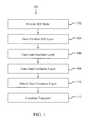
- FIG. 1is a flow diagram illustrating a fabrication method of the invention
- FIGS. 2 a, 3 a, 4 a, 5 a, 6 a, and 7 aare top plan views of an embodiment of a semiconductor structure of the invention during the fabrication method of FIG. 1;
- FIGS. 2 b, 3 b, 4 b, 5 b, 6 b, and 7 bare cross-sectional side views of an embodiment of a semiconductor structure of the invention during the fabrication method of FIG. 1 taken along lines 2 b — 2 b, 3 b — 3 b, 4 b — 4 b, 5 b — 5 b, 6 b — 6 b, and 7 b — 7 b of FIGS. 2 a, 3 a, 4 a, 5 a, 6 a, and 7 a respectively;
- FIG. 8is an embodiment of a FinFET CMOS inverter of the invention.
- FIG. 9is a circuit diagram of the FinFET CMOS inverter of FIG. 8 .
- the present inventionexploits semiconductor physics by utilizing various crystal planes for FET current channels in order to optimize mobility and/or to reduce mobility in specific devices depending on the particular application.
- Individuals skilled in the art of semiconductor physicsmay wish to proceed with to the Detailed Description section of this specification.
- those individuals who are new to crystal lattice planes and directions,should read the following Overview section in order to best understand the benefits and advantages of the present invention.
- the atoms which make up the solidare spatially arranged in a periodic fashion called a lattice.
- the crystal latticealways contains a volume which is representative of the entire lattice and it is regularly repeated throughout the crystal.
- the directions in a latticeare expressed as a set of three integers with the same relationship as the components of a vector in that direction.
- the three vector componentsare given in multiples of the basic vectors. For example, in cubic lattices, such as silicon that has a diamond crystal lattice, a body diagonal exists along the [111] direction with the [ ] brackets denoting a specific direction.
- the designation of the direction ⁇ 100>includes the equivalent [100], [010], and [001] directions. Since these directions will also be on the negative side of the origin (as arbitrarily defined), unless specifically stated or shown otherwise in this application, a crystal direction includes both positive and negative integers. Accordingly, for example, the designation of the direction ⁇ 100> includes the [ ⁇ 100], [0-10], and [00-1] directions in addition to the [100], [010], and [001] directions.
- Planes in a crystalalso may be determined with a set of three integers. They are used to define a set of parallel planes and each set of three integers in ( ) parentheses identify a specific plane. A plane identified by a specific set of three integers is perpendicular to a direction identified by the identical three integers. For example, the proper designation for a plane perpendicular to the [100] direction is (100). Thus, if either a direction or a plane of a cubic lattice is known, its perpendicular counterpart may be quickly determined without calculation.
- the (100), (010), and (001) planesare planes of equivalent symmetry.
- a plane and all of its equivalent planesare denoted by ⁇ ⁇ parentheses.
- the designation of the plane ⁇ 100 ⁇includes the equivalent (100), (010), and (001) planes.
- a crystal plane in this applicationincludes both positive and negative integers unless specifically stated or shown otherwise. Accordingly, for example, the designation of the plane ⁇ 100 ⁇ includes the ( ⁇ 100), (0-10), and (00-1) planes in addition to the (100), (010), and (001) planes.
- CMOScomplimentary metal oxide semiconductor
- FinFETsfin field effect transistors
- FIGS. 2 a - 7 aare top plan views and FIGS. 2 b - 7 b are cross-sectional views, the respective views depicting various stages during method 100 .
- fabrication method 100 of present inventionmay form CMOS FinFETs by: providing a substrate having a surface oriented on a first crystal plane that enables subsequent crystal planes for channels to be utilized; forming a first transistor so that a sidewall of a first fin body forms a first current channel and so that the sidewall of the first fin body is oriented on a second crystal plane to provide a first carrier mobility; and forming a second transistor so that a sidewall of a second fin body forms a second current channel and so that the sidewall of the second fin body is oriented on a third crystal plane to provide a second carrier mobility that is different from the first carrier mobility.
- first step 102 of method 100is to provide an appropriate substrate having a surface oriented on a first crystal plane that enables subsequent crystal planes for FET current channels to be utilized, such as a ⁇ 110 ⁇ crystal plane for example.
- the proper alignment of the crystal latticehas a large effect on the material properties of the substrate, including its electrical properties (e.g. its carrier mobility properties) and how it reacts to other materials and chemical processing.
- providing a substrate having a surface oriented on a ⁇ 110 ⁇ crystal plane for exampleenables method 100 to form FinFETs in a manner that for the first time enables subsequent crystal planes for the FET current channels to be utilized.
- method 100 of the present inventionmay be used to fabricate any combination of n-channel FinFETs (NFETs) and p-channel FinFETs (PFETs) on any combination of surface planes, such as the ⁇ 100 ⁇ , ⁇ 110 ⁇ and ⁇ 111 ⁇ for example.
- the electron mobilitywill be optimized for an NFET on ⁇ 100 ⁇ or ⁇ 110 ⁇ and the hole mobility will be optimized for a PFET on ⁇ 111 ⁇ , while the electron mobility will be reduced for an NFET on ⁇ 111 ⁇ and the hole mobility will be reduced for a PFET on ⁇ 100 ⁇ .
- the equivalent planes accessible by method 100may be represented by the plane ⁇ n n m ⁇ or the plane ⁇ a a b ⁇ for example, wherein n, m, a, b, etc. are any integer, such that the plane in ⁇ n n m ⁇ and the plane ⁇ a a b ⁇ are not equivalent by a symmetry transformation.
- method 100 of the present inventionmay be used to optimize carrier mobility and/or may be used to reduce mobility in specific devices, if needed.
- substrate 200may comprise wafer 202 that underlies buried insulator 204 that underlies semiconductor layer 206 . Therefore, for example, substrate 200 may comprise a single crystal silicon-on-insulator (SOI) wafer. However, other substrate 200 embodiments may be used, such as a non-SOI wafer comprising only wafer 202 (i.e., a chip) for example. When a non-SOI wafer embodiment is used, the processing remains otherwise identical to that of a SOI wafer embodiment, except as noted.
- SOIsilicon-on-insulator
- Wafer 202may be composed of any appropriate semiconducting material, including, but not limited to: Si, Ge, GaP, InAs, InP, SiGe, GaAs, or other III/V compounds. Wafer 202 has a surface oriented on a first crystal plane that allows subsequent surface planes for FET current channels to be utilized. For the exemplary purposes of this disclosure, wafer 202 may comprise single crystal silicon and have a surface oriented on a ⁇ 110 ⁇ crystal plane.
- Buried insulator 204may be formed on wafer 202 using thermal oxidation, such as rapid-thermal processing (RTP) or furnace processing for example, or other techniques known in the art.
- Buried insulator 204may comprise any insulative material, such as Buried Oxide (BOX).
- BOXBuried Oxide
- any type and/or combination of buried insulatorsmay be used for buried insulator 204 .
- Semiconductor layer 206may be formed on buried insulator 204 by any technique known in the art, and may comprise any semiconductor material. Additionally, semiconductor layer 206 has a surface oriented on a first crystal plane that allows subsequent surface planes for FET current channels to be utilized. For the exemplary purposes of this disclosure, semiconductor layer 206 comprises a single crystal silicon-on-insulator (SOI) layer having a surface oriented on a ⁇ 110 ⁇ crystal plane. Semiconductor layer 206 may also have any thickness. For the exemplary purposes of this disclosure, semiconductor layer 206 may have a thickness between approximately 20 nm-160 nm. As will be made clear, semiconductor layer 206 thickness may define the height of the fins.
- SOIsilicon-on-insulator
- step 104 of method 100is to form one or more fins from semiconductor layer 206 .
- a portion of each fini.e., a fin body
- the finsmay be formed in any of the previously proposed techniques. Accordingly, for the exemplary purposes of this disclosure, fins may be formed from semiconductor layer 206 in step 104 in the following manner.
- the first stepis to deposit hard mask film 208 as depicted in FIGS. 2 a - 2 b.
- Hard mask film 208acts as an etch stop layer and will be used throughout the CMOS FinFET fabrication process when needed.
- hard mask film 208may be silicon dioxide (SiO 2 ) or silicon nitride (Si 3 N 4 ).
- a next stepis implemented to pattern and etch hard mask film 208 by any technique known in the art.
- a suitable thin layer of photoresist (PR)may be used to cover the surface of hard mask film 208 .
- PRphotoresist
- a mask with a predetermined orientationmay be used to generate a specific pattern of narrow lines on the PR overlying hard mask film 208 .
- the particular FinFET plane(the crystal plane that the electrons or holes are associated with) is defined by how the mask is oriented to facilitate etching that fin into substrate 200 , as opposed to the particular crystal plane substrate 200 surface is oriented on.
- selecting and implementing simple and predetermined mask changes according to method 100 of the present inventionprovides flexibility within substrate 200 to designate particular crystal planes for different devices.
- method 100 of the present inventionmay be used to fabricate any combination of NFETs and PFETs on any combination of surface planes represented by the plane ⁇ n n m ⁇ or the plane ⁇ a a b ⁇ for example, wherein n, m, a, b, etc. are any integer, such that the plane ⁇ n n m ⁇ and the plane ⁇ a a b ⁇ are not equivalent by a symmetry transformation.
- method 100 of the present inventionmay be used to optimize carrier mobility and/or may be used to reduce mobility in specific devices, if needed.
- a suitable directional etchmay be performed through hard mask film 208 to form narrow lines in hard mask film 208 , which typically have a width in the range of approximately 0.3 nm to 40 nm. As will be made clear, the width of hard mask film 208 narrow lines translates into the thickness of the fins.
- the PRis then stripped away by a suitable chemical process, thereby resulting in hard mask film 208 narrow lines on semiconductor layer 206 as depicted in FIGS. 3 a - 3 b.
- the next stepis to anisotropically etch semiconductor layer 206 using hard mask film 208 narrow lines, thereby forming the fins.
- Thismay be done using a suitable reactive ion etch (RIE) process that etches semiconductor layer 206 , stopping on buried insulator 204 .
- RIEreactive ion etch
- finsremain and comprise portions of semiconductor layer 206 with overlying hard mask film 208 narrow lines.
- the finsmay have opposing vertical sidewalls 207 that are substantially perpendicular to buried insulator 204 .
- the predetermined orientation of the mask in a previous stephas resulted in sidewalls 207 being oriented on particular crystal planes in order to optimize carrier mobility for both carrier types and/or reduce mobility in specific devices as needed, thereby maintaining an acceptable and/or desired performance. Accordingly, sidewalls 207 of the fin bodies may be oriented on a crystal planes that provide different carrier mobilities.
- Sidewalls 207 of the fin bodiesmay also be oriented on a ⁇ n n m ⁇ plane, wherein n and m are any integer, and/or sidewalls 207 of the fin bodies may be oriented on a ⁇ a a b ⁇ plane, wherein a and b are any integer, such that the plane ⁇ n n m ⁇ and the plane ⁇ a a b ⁇ are not equivalent by a symmetry transformation. Additionally, sidewalls 207 of the fin bodies may oriented on crystal planes that provide one of an optimized carrier mobility and a non-optimized (i.e. anything less than optimized) carrier mobility.
- sidewalls 207 of the fin bodiesmay be oriented on a crystal planes that are not equivalent to one another by a symmetry transformation. Moreover, sidewalls 207 of the fin bodies may oriented on one of a ⁇ 100 ⁇ crystal plane, a ⁇ 110 ⁇ crystal plane, and a ⁇ 111 ⁇ crystal plane.
- the finsmay then be doped as needed. Typically, this may include an ion implantation into the fins so as to form P-well structures and N-well structures.
- P-well structures and N-well structuresare formed to allow the integration of NFETs and PFETs in a common substrate.
- P, As and Sb, for exampleare well suited for PFETs.
- B, In and Ga, for example,are well suited for NFETs.
- Ion implantationis typically designed to achieve a concentration of between 1 ⁇ 10 17 cm ⁇ 3 to 5 ⁇ 10 18 cm ⁇ 3 for example.
- ion implantationmay comprise an angled implant into exposed opposing vertical sidewalls 207 of semiconductor layer 206 , and would serve to properly dope the fins.
- a deposit/etch oxide processis used to deposit SiO 2 exclusively on the bottom horizontal surfaces of etched wafer 202 of a thickness approximately one-quarter the height of the etched fins.
- the oxidemay be doped with, for example, B in the case of NFETs or P in the case of PFETs, and some portion of the dopant out-diffused into those portions of the fins immediately adjacent to the doped oxide. This serves to suppress leakage in what will be non-gated sidewalls of the fins, from source to drain.
- gated sidewalls of the fin bodiesmay form current channels in between the exposed (non-gated) portions of the fins comprising source and drain regions.
- FinFET sidewalls forming current channelsmay be oriented on a ⁇ n n m ⁇ plane, where n and m are any integer, or on a ⁇ a a b ⁇ plane, where a and b are any integer, such that the ⁇ n n m ⁇ plane and the ⁇ a a b ⁇ plane are not equivalent by a symmetry transformation.
- the sidewallsmay be oriented on crystal planes that provide different carrier mobilities.
- the sidewallsmay be oriented on crystal planes that provide one of an optimized carrier mobility and a non-optimized carrier mobility.
- FinFET sidewallsmay be oriented on one of a ⁇ 100 ⁇ crystal plane, a ⁇ 110 ⁇ crystal plane, and a ⁇ 111 ⁇ crystal plane.
- the ⁇ 111 ⁇ crystal planeoptimizes carrier mobility for a PFET, and both the ⁇ 100 ⁇ crystal plane and the ⁇ 110 ⁇ crystal plane optimize carrier mobility for an NFET.
- the ⁇ 100 ⁇ crystal planefails to optimize carrier mobility for a PFET
- the ⁇ 111 ⁇ crystal planefails to optimize carrier mobility for an NFET.
- gate insulator layers 210are formed on opposing vertical sidewalls 207 and opposing end walls of the fins (i.e., semiconductor layer 206 portions) as depicted in FIGS. 5 a - 5 b.
- Gate insulator layers 210may be formed by thermal oxidation, typically at 750-800° C., or alternatively, may be formed by depositing a dielectric film.
- gate insulator layers 210may be SiO 2 , a nitrided oxide material, a high-K dielectric material, or combinations thereof, as known in the art.
- step 108 of method 100is to form gate conductor layer 212 overlying hard mask film 208 narrow lines, oxide layers 210 , and buried insulator 204 .
- Gate conductor layer 212may be any suitable conducting material, typically a polycrystalline silicon material, although amorphous silicon, a combination of amorphous silicon and polysilicon, polysilicon-germanium, or any other appropriate material may be used to form gate conductor layer 212 .
- a metal gate conductor layer 212such as W, Mo, or Ta, or any other refractory metal, or alternatively a silicided gate conductor comprising polysilicon added with Ni or Co.
- gate conductor layer 212encompasses a silicon material
- such layersmay be deposited as a doped layer (in-situ doping).
- gate conductor layer 212is a metal layer
- such layersmay be deposited using physical vapor or chemical vapor deposition methods or any other technique known in the arc. In this manner, gate structures are formed adjacent to oxide layers 210 firmed on opposing vertical sidewalls 207 of the fins formed by semiconductor layer 206 portions.
- step 110 of method 100is to pattern gate conductor layer 212 .
- hard mask film 214is formed and patterned to facilitate the patterning of gate conductor layer 212 .
- hard mask film 214 materialmay be SiO 2 or Si 3 N 4 .
- gate conductor layer 212is patterned. Accordingly, gate conductor layer 212 may be patterned and structured using well known photolithography and etching techniques to form the gate stack, i.e, using hard mask film 214 caps as an etch mask during a directional etching of gate conductor layer 212 .
- the patterning and structuringalso leaves portions of gate conductor layer 212 , which define the gate structures adjacent the fin bodies.
- FIGS. 7 a - 7 ban embodiment of the present invention is depicted having a minimum of complexity.
- This depicted embodiment of the present inventionis at a stage of a process flow technique modified by a fabrication method of the present invention for forming CMOS FinFETs on the same substrate utilizing various crystal planes for FET current channels.
- wafer 202is depicted with an overlying buried insulator 204 .
- semiconductor layer 206 portionscomprising the fins with overlying hard mask film 208 narrow lines.
- Gate insulator layers 210are formed on opposing vertical sidewalls 207 and opposing end walls of the fins.
- gate stacksthat comprise: gate insulator layers 210 portions formed on opposing vertical sidewalls 207 portions of the fin bodies; gate conductor layer 212 portions (i.e., gates) overlying gate insulator layers 210 portions and hard mask film 208 narrow line portions overlying the fin bodies; and hard mask film 214 caps overlying gate conductor layer 212 portions.
- PFET sidewallsare oriented on a ⁇ 111 ⁇ crystal plane, which provides the optimum carrier mobility for a PFET, while NFET sidewalls are oriented on a ⁇ 100 ⁇ crystal plane, which provides an optimum carrier mobility for a NFET.
- gate conductor layer 212 portionsdo not connect with one another, but in other embodiments, such as the embodiment depicted in FIG. 8 that will hereinafter be described, similar gate conductor layer 314 portion is unitary.
- FIGS. 7 a - 7 b or any other FinFET embodiments of the present invention utilizing different crystal planes for FET current channelsmay be completed according to step 112 of method 100 . Accordingly, exposed portions of the fins may be doped to form S/D regions.
- the S/D regionsmay define, in semiconductor layer 206 portions comprising the fin bodies, channel regions underlying the gate stacks. Formation of the S/D regions may be accomplished using any of the variety of methods that have been developed to form SD region and that are tailored for specific performance requirements. There are many such methods for forming S/D regions having various levee of complexity.
- lightly doped S/fl regions or other S/D regionsmay be formed.
- NFETStypically P, As, or Sb for example is used for the S/D implants in the range of 1 to 5 keV and a dose of 5 ⁇ 10 14 to 2 ⁇ 10 15 cm ⁇ 3 .
- PFETStypically B, In, or Ga for example is used for the S/D implants in the range of 0.5 to 3 key and dose of 5 ⁇ 10 14 to 2 ⁇ 10 15 cm ⁇ 3 .
- extension and halo implantsmay be formed that improve Short Channel Effects (SCE).
- SCEShort Channel Effects
- NFETstypically B, In, or Ga may be used for the halo implants with energies in the range of 5 to 15 keV and a dose of 1 ⁇ 10 13 to 8 ⁇ 10 13 cm ⁇ 3 .
- P, As, or Sbmay be used for the halos, with energies from 20 to 45 keV and dose of 1 ⁇ 10 13 to 8 ⁇ 10 13 cm ⁇ 3 .
- contacts to sources, drains, and gatesmay then be formed.
- an inter metal dielectricmay be deposited and planarized typically using a CMP process.
- Contact holesmay then be structured and etched using an anisotropic process (e.g. RIE) or the like.
- the contact holesmay be filled using any conducting material, such as doped polysilicon, silicide (e.g. WSi), metals (e.g. Au, Al, Mo, W, Ta, Ti, Cu, or ITO (indium-tin oxide)), or the like, being deposited by evaporation, sputtering, or other known techniques, thereby forming S/D contacts.
- the first metal layermay be deposited and structured using a RIE process or the like.
- the structuring of the first metal layermay be done following a damacene process flow.
- CMOS FinFETs on the same substrate utilizing various crystal planes for FET current channels according to the present inventionmay be used in many different kinds of circuits, such as high performance logic, low power logic or high density memory devices, including high density multi-gigabit DRAMs.
- inventive CMOS FinFETsmay readily be combined with other elements, such as for example capacitors, resistors, diodes, memory cells and so forth.
- CMOS inverter 300is depicted in FIG. 8 and a circuit diagram relating the various elements of FinFET CMOS inverter 300 is depicted in FIG. 9 .
- FinFET CMOS inverter 300may be fabricated by method 100 as previously described, and as such, it includes all of the benefits and advantages outlined previously in conjunction with the description of method 100 .
- FinFET CMOS inverter 300may be formed from a pair comprising PFET 302 and NFET 308 .
- PFET 302 and NFET 308are: joined at their respective drains 306 and 312 by local wiring 316 portion where the output (Out) is taken; and joined at their respective gates 305 and 311 by gate conductor 314 portion where the input (In) is taken.
- the pairis supplied with power supply voltage (Vdd) along local wiring 317 portion connected to source 304 of PFET 302 , and the pair is connected to ground (Gnd) from source 310 of NFET 308 connected to local wiring 318 portion.
- Vddpower supply voltage
- Gndground
- FinFET CMOS inverter 300acts as a switching circuit, since PFET 302 has exactly the opposite characteristics of NFET 308 . Generally, PFET 302 and NFET 308 are switched by the input voltage. When the input is low, PFET 302 turns on. On the other hand, when the input is high, NFET 308 is turned on. PFET 302 and NFET 308 do not switch on at the same time, which prevents DC current from Vdd to the Gnd. Particularly, as depicted in FIG.
- PFET 302is formed so that it is oriented on a ⁇ 111 ⁇ crystal plane and NFET 308 is formed so that it is oriented on a ⁇ 100 ⁇ crystal plane, in contrast to conventional planar CMOS that cannot utilize different surface planes for different devices. Therefore, by providing a substrate surface oriented on a 110 crystal plane and implementing simple mask changes that provide flexibility within the substrate to designate particular crystal planes for different devices, FinFET CMOS inverter 300 achieves an optimum mobility for holes and electrons, thereby increasing the switching speed of PFET 302 and NFET 308 .
- the present inventionmay provide CMOS FinFETs on the same substrate utilizing various crystal planes for FET current channels without any complex device engineering. Additionally, since rotating a FinFET design according to the present invention, unlike rotating planar FET designs, changes the actual planar surface of the device, a mobility change may be realized. Thus, by forming multiple FinFETs on various crystal planes on the same substrate, multiple different carrier mobilities may be realized in order to optimize mobility and/or reduce mobility in specific devices as needed, thereby maintaining an acceptable and/or desired performance.
Landscapes
- Metal-Oxide And Bipolar Metal-Oxide Semiconductor Integrated Circuits (AREA)
Abstract
Description
Claims (13)
Priority Applications (2)
| Application Number | Priority Date | Filing Date | Title |
|---|---|---|---|
| US10/011,846US6657259B2 (en) | 2001-12-04 | 2001-12-04 | Multiple-plane FinFET CMOS |
| US10/645,063US6815277B2 (en) | 2001-12-04 | 2003-08-21 | Method for fabricating multiple-plane FinFET CMOS |
Applications Claiming Priority (1)
| Application Number | Priority Date | Filing Date | Title |
|---|---|---|---|
| US10/011,846US6657259B2 (en) | 2001-12-04 | 2001-12-04 | Multiple-plane FinFET CMOS |
Related Child Applications (1)
| Application Number | Title | Priority Date | Filing Date |
|---|---|---|---|
| US10/645,063DivisionUS6815277B2 (en) | 2001-12-04 | 2003-08-21 | Method for fabricating multiple-plane FinFET CMOS |
Publications (2)
| Publication Number | Publication Date |
|---|---|
| US20030102497A1 US20030102497A1 (en) | 2003-06-05 |
| US6657259B2true US6657259B2 (en) | 2003-12-02 |
Family
ID=21752217
Family Applications (2)
| Application Number | Title | Priority Date | Filing Date |
|---|---|---|---|
| US10/011,846Expired - LifetimeUS6657259B2 (en) | 2001-12-04 | 2001-12-04 | Multiple-plane FinFET CMOS |
| US10/645,063Expired - LifetimeUS6815277B2 (en) | 2001-12-04 | 2003-08-21 | Method for fabricating multiple-plane FinFET CMOS |
Family Applications After (1)
| Application Number | Title | Priority Date | Filing Date |
|---|---|---|---|
| US10/645,063Expired - LifetimeUS6815277B2 (en) | 2001-12-04 | 2003-08-21 | Method for fabricating multiple-plane FinFET CMOS |
Country Status (1)
| Country | Link |
|---|---|
| US (2) | US6657259B2 (en) |
Cited By (97)
| Publication number | Priority date | Publication date | Assignee | Title |
|---|---|---|---|---|
| US20030102518A1 (en)* | 2001-12-04 | 2003-06-05 | International Business Machines Corporation | Finfet SRAM cell using low mobility plane for cell stability and method for forming |
| US20040048424A1 (en)* | 2002-09-05 | 2004-03-11 | Taiwan Semiconductor Manufacturing Company | Method of forming an N channel and P channel FINFET device on the same semiconductor substrate |
| US20040126975A1 (en)* | 2002-11-08 | 2004-07-01 | Ahmed Shibly S. | Double gate semiconductor device having separate gates |
| US6787476B1 (en)* | 2003-08-04 | 2004-09-07 | Advanced Micro Devices, Inc. | Etch stop layer for etching FinFET gate over a large topography |
| US20040197975A1 (en)* | 2003-01-23 | 2004-10-07 | Zoran Krivokapic | Narrow fin finfet |
| US20040198031A1 (en)* | 2003-04-03 | 2004-10-07 | Ming-Ren Lin | Method for forming structures in finfet devices |
| US6812119B1 (en)* | 2003-07-08 | 2004-11-02 | Advanced Micro Devices, Inc. | Narrow fins by oxidation in double-gate finfet |
| US6815268B1 (en)* | 2002-11-22 | 2004-11-09 | Advanced Micro Devices, Inc. | Method for forming a gate in a FinFET device |
| US20040222477A1 (en)* | 2003-05-05 | 2004-11-11 | International Business Machines Corporation | Multi-height finfets |
| US20040245579A1 (en)* | 2001-12-13 | 2004-12-09 | Tadahiro Ohmi | Complementary mis device |
| US20040266076A1 (en)* | 2003-06-26 | 2004-12-30 | International Business Machines Corporation | HYBRID PLANAR AND FinFET CMOS DEVICES |
| US6855989B1 (en) | 2003-10-01 | 2005-02-15 | Advanced Micro Devices, Inc. | Damascene finfet gate with selective metal interdiffusion |
| US6867460B1 (en)* | 2003-11-05 | 2005-03-15 | International Business Machines Corporation | FinFET SRAM cell with chevron FinFET logic |
| US20050093067A1 (en)* | 2003-04-30 | 2005-05-05 | Yee-Chia Yeo | Semiconductor-on-insulator chip incorporating strained-channel partially-depleted, fully-depleted, and multiple-gate transistors |
| US20050104091A1 (en)* | 2003-11-04 | 2005-05-19 | Tabery Cyrus E. | Self aligned damascene gate |
| US6936882B1 (en)* | 2003-07-08 | 2005-08-30 | Advanced Micro Devices, Inc. | Selective silicidation of gates in semiconductor devices to achieve multiple threshold voltages |
| US20050191795A1 (en)* | 2004-03-01 | 2005-09-01 | Dureseti Chidambarrao | Method of manufacture of FinFET devices with T-shaped fins and devices manufactured thereby |
| US20050215014A1 (en)* | 2004-03-23 | 2005-09-29 | Young-Joon Ahn | Complementary metal oxide semiconductor (CMOS) transistors having three-dimensional channel regions and methods of forming same |
| US20050224875A1 (en)* | 2004-03-31 | 2005-10-13 | International Business Machines Corporation | High mobility plane cmos soi |
| US20050239242A1 (en)* | 2004-04-23 | 2005-10-27 | International Business Machines Corporation | structure and method of manufacturing a finFet device having stacked fins |
| US20050255656A1 (en)* | 2004-05-17 | 2005-11-17 | Hee-Soo Kang | Field effect transistor (FET) devices and methods of manufacturing FET devices |
| US20060001093A1 (en)* | 2004-03-12 | 2006-01-05 | Tenko Yamashita | Silicon-on insulator (SOI) substrate having dual surface crystallographic orientations and method of forming same |
| US20060044915A1 (en)* | 2004-09-01 | 2006-03-02 | Park Ji-Hoon | Flash memory device using semiconductor fin and method thereof |
| US20060049460A1 (en)* | 2004-05-28 | 2006-03-09 | Hung-Wei Chen | CMOS logic gate fabricated on hybrid crystal orientations and method of forming thereof |
| US20060128071A1 (en)* | 2002-12-20 | 2006-06-15 | Rankin Jed H | Integrated antifuse structure for finfet and cmos devices |
| US20060186416A1 (en)* | 2005-02-24 | 2006-08-24 | International Business Machines Corporation | Multiple layer and crystal plane orientation semiconductor substrate |
| US20060226487A1 (en)* | 2003-08-18 | 2006-10-12 | Yee-Chia Yeo | Resistor with reduced leakage |
| US7148526B1 (en) | 2003-01-23 | 2006-12-12 | Advanced Micro Devices, Inc. | Germanium MOSFET devices and methods for making same |
| US20060281236A1 (en)* | 2003-10-02 | 2006-12-14 | Suman Datta | Method and apparatus for improving stability of a 6T CMOS SRAM cell |
| US20060289940A1 (en)* | 2005-06-28 | 2006-12-28 | Hyun Jae-Woong | Fin FET CMOS device, method of manufacturing the same, and memory including fin FET CMOS device |
| CN1298056C (en)* | 2004-07-09 | 2007-01-31 | 北京大学 | A CMOS circuit structure situated on SOI substrate and manufacturing method thereof |
| US20070134878A1 (en)* | 2005-12-09 | 2007-06-14 | Intel Corporation | Non-planar microelectronic device having isolation element to mitigate fringe effects and method to fabricate same |
| US20070131983A1 (en)* | 2005-12-13 | 2007-06-14 | Intel Corporation | Tri-gate integration with embedded floating body memory cell using a high-K dual metal gate |
| US20070138514A1 (en)* | 2005-12-21 | 2007-06-21 | Chang Peter L | Integration of planar and tri-gate devices on the same substrate |
| US20070148926A1 (en)* | 2005-12-28 | 2007-06-28 | Intel Corporation | Dual halo implant for improving short channel effect in three-dimensional tri-gate transistors |
| US7241653B2 (en) | 2003-06-27 | 2007-07-10 | Intel Corporation | Nonplanar device with stress incorporation layer and method of fabrication |
| US7262104B1 (en) | 2004-06-02 | 2007-08-28 | Advanced Micro Devices, Inc. | Selective channel implantation for forming semiconductor devices with different threshold voltages |
| US20070231997A1 (en)* | 2006-03-31 | 2007-10-04 | Doyle Brian S | Stacked multi-gate transistor design and method of fabrication |
| US20070231984A1 (en)* | 2006-03-31 | 2007-10-04 | Metz Matthew V | Uniform silicide metal on epitaxially grown source and drain regions of three-dimensional transistors |
| US20070235763A1 (en)* | 2006-03-29 | 2007-10-11 | Doyle Brian S | Substrate band gap engineered multi-gate pMOS devices |
| CN100356525C (en)* | 2003-12-12 | 2007-12-19 | 国际商业机器公司 | Strained finFETs and method of manufacture |
| US7329913B2 (en) | 2003-12-30 | 2008-02-12 | Intel Corporation | Nonplanar transistors with metal gate electrodes |
| US20080054359A1 (en)* | 2006-08-31 | 2008-03-06 | International Business Machines Corporation | Three-dimensional semiconductor structure and method for fabrication thereof |
| US20080061371A1 (en)* | 2004-05-17 | 2008-03-13 | Samsung Electronics Co., Ltd. | Field effect transistor (fet) devices and methods of manufacturing fet devices |
| US7348284B2 (en) | 2004-08-10 | 2008-03-25 | Intel Corporation | Non-planar pMOS structure with a strained channel region and an integrated strained CMOS flow |
| US7354843B2 (en) | 2003-07-25 | 2008-04-08 | Taiwan Semiconductor Manufacturing Company, Ltd. | Method of forming a capacitor that includes forming a bottom electrode in a strained silicon layer |
| KR100823874B1 (en)* | 2006-12-28 | 2008-04-21 | 경북대학교 산학협력단 | High Density FUNI Field Effect Transistor with Low Leakage Current and Manufacturing Method Thereof |
| US7361958B2 (en) | 2004-09-30 | 2008-04-22 | Intel Corporation | Nonplanar transistors with metal gate electrodes |
| US20080093690A1 (en)* | 2006-10-19 | 2008-04-24 | Frank Reichenbach | Micromechanical component having a monolithically integrated circuit and method for manufacturing a component |
| US20080097346A1 (en)* | 2006-09-19 | 2008-04-24 | Alcon, Inc. | Trocar cannula |
| US20080121949A1 (en)* | 2006-11-06 | 2008-05-29 | Anderson Brent A | Semiconductor structures incorporating multiple crystallographic planes and methods for fabrication thereof |
| US20080121998A1 (en)* | 2006-09-15 | 2008-05-29 | Kavalieros Jack T | Apparatus and method for selectively recessing spacers on multi-gate devices |
| US7396711B2 (en) | 2005-12-27 | 2008-07-08 | Intel Corporation | Method of fabricating a multi-cornered film |
| US7432557B1 (en) | 2003-07-08 | 2008-10-07 | Advanced Micro Devices, Inc. | FinFET device with multiple channels |
| US7442967B2 (en) | 2003-08-12 | 2008-10-28 | Taiwan Semiconductor Manufacturing Company, Ltd. | Strained channel complementary field-effect transistors |
| US7449373B2 (en) | 2006-03-31 | 2008-11-11 | Intel Corporation | Method of ion implanting for tri-gate devices |
| US7456476B2 (en) | 2003-06-27 | 2008-11-25 | Intel Corporation | Nonplanar semiconductor device with partially or fully wrapped around gate electrode and methods of fabrication |
| US7479421B2 (en) | 2005-09-28 | 2009-01-20 | Intel Corporation | Process for integrating planar and non-planar CMOS transistors on a bulk substrate and article made thereby |
| US7498225B1 (en) | 2003-12-04 | 2009-03-03 | Advanced Micro Devices, Inc. | Systems and methods for forming multiple fin structures using metal-induced-crystallization |
| US20090065868A1 (en)* | 2007-09-07 | 2009-03-12 | Christian Russ | Electronic Circuit and Method of Manufacturing an Electronic Circuit |
| US7518196B2 (en) | 2005-02-23 | 2009-04-14 | Intel Corporation | Field effect transistor with narrow bandgap source and drain regions and method of fabrication |
| US7525160B2 (en) | 2005-12-27 | 2009-04-28 | Intel Corporation | Multigate device with recessed strain regions |
| US7547637B2 (en) | 2005-06-21 | 2009-06-16 | Intel Corporation | Methods for patterning a semiconductor film |
| US7550333B2 (en) | 2004-10-25 | 2009-06-23 | Intel Corporation | Nonplanar device with thinned lower body portion and method of fabrication |
| US7579280B2 (en) | 2004-06-01 | 2009-08-25 | Intel Corporation | Method of patterning a film |
| US7646068B2 (en) | 2003-08-15 | 2010-01-12 | Taiwan Semiconductor Manufacturing Company, Ltd. | Structure and method of a strained channel transistor and a second semiconductor component in an integrated circuit |
| US20100025826A1 (en)* | 2008-07-30 | 2010-02-04 | Qimonda Ag | Field Effect Transistors with Channels Oriented to Different Crystal Planes |
| US7679134B1 (en) | 2002-11-26 | 2010-03-16 | Globalfoundries | FinFET device with multiple fin structures |
| US7700470B2 (en) | 2006-09-22 | 2010-04-20 | Intel Corporation | Selective anisotropic wet etching of workfunction metal for semiconductor devices |
| US7736956B2 (en) | 2005-08-17 | 2010-06-15 | Intel Corporation | Lateral undercut of metal gate in SOI device |
| US20100155801A1 (en)* | 2008-12-22 | 2010-06-24 | Doyle Brian S | Integrated circuit, 1T-1C embedded memory cell containing same, and method of manufacturing 1T-1C memory cell for embedded memory application |
| US7745279B2 (en) | 2003-07-25 | 2010-06-29 | Taiwan Semiconductor Manufacturing Company, Ltd. | Capacitor that includes high permittivity capacitor dielectric |
| US20100163945A1 (en)* | 2008-12-30 | 2010-07-01 | Kavalieros Jack T | Embedded memory cell and method of manufacturing same |
| US7759179B2 (en) | 2008-01-31 | 2010-07-20 | International Business Machines Corporation | Multi-gated, high-mobility, density improved devices |
| US7781771B2 (en) | 2004-03-31 | 2010-08-24 | Intel Corporation | Bulk non-planar transistor having strained enhanced mobility and methods of fabrication |
| US7808051B2 (en) | 2008-09-29 | 2010-10-05 | Taiwan Semiconductor Manufacturing Company, Ltd. | Standard cell without OD space effect in Y-direction |
| US7859053B2 (en) | 2004-09-29 | 2010-12-28 | Intel Corporation | Independently accessed double-gate and tri-gate transistors in same process flow |
| US7867860B2 (en) | 2003-07-25 | 2011-01-11 | Taiwan Semiconductor Manufacturing Company, Ltd. | Strained channel transistor formation |
| US20110021010A1 (en)* | 2009-07-27 | 2011-01-27 | International Business Machines Corporation | Method for double pattern density |
| US7879675B2 (en) | 2005-03-14 | 2011-02-01 | Intel Corporation | Field effect transistor with metal source/drain regions |
| US7888201B2 (en) | 2003-11-04 | 2011-02-15 | Taiwan Semiconductor Manufacturing Company, Ltd. | Semiconductor-on-insulator SRAM configured using partially-depleted and fully-depleted transistors |
| US7898041B2 (en) | 2005-06-30 | 2011-03-01 | Intel Corporation | Block contact architectures for nanoscale channel transistors |
| US7902014B2 (en) | 2005-09-28 | 2011-03-08 | Intel Corporation | CMOS devices with a single work function gate electrode and method of fabrication |
| US7915167B2 (en) | 2004-09-29 | 2011-03-29 | Intel Corporation | Fabrication of channel wraparound gate structure for field-effect transistor |
| US7943961B2 (en) | 2008-03-13 | 2011-05-17 | Taiwan Semiconductor Manufacturing Company, Ltd. | Strain bars in stressed layers of MOS devices |
| US7989280B2 (en) | 2005-11-30 | 2011-08-02 | Intel Corporation | Dielectric interface for group III-V semiconductor device |
| US8084818B2 (en) | 2004-06-30 | 2011-12-27 | Intel Corporation | High mobility tri-gate devices and methods of fabrication |
| US8217450B1 (en) | 2004-02-03 | 2012-07-10 | GlobalFoundries, Inc. | Double-gate semiconductor device with gate contacts formed adjacent sidewalls of a fin |
| US8338256B2 (en) | 2010-07-08 | 2012-12-25 | International Business Machines Corporation | Multi-gate transistor having sidewall contacts |
| US8362566B2 (en) | 2008-06-23 | 2013-01-29 | Intel Corporation | Stress in trigate devices using complimentary gate fill materials |
| US8558278B2 (en) | 2007-01-16 | 2013-10-15 | Taiwan Semiconductor Manufacturing Company, Ltd. | Strained transistor with optimized drive current and method of forming |
| US8617945B2 (en) | 2006-08-02 | 2013-12-31 | Intel Corporation | Stacking fault and twin blocking barrier for integrating III-V on Si |
| US9190465B2 (en) | 2012-01-05 | 2015-11-17 | Globalfoundries Inc. | FinFET device |
| US9275911B2 (en) | 2012-10-12 | 2016-03-01 | Globalfoundries Inc. | Hybrid orientation fin field effect transistor and planar field effect transistor |
| US9337307B2 (en) | 2005-06-15 | 2016-05-10 | Intel Corporation | Method for fabricating transistor with thinned channel |
| TWI566273B (en)* | 2013-06-13 | 2017-01-11 | 聯華電子股份有限公司 | Method of fabricating semiconductor pattern |
| US11342327B2 (en)* | 2017-12-28 | 2022-05-24 | Intel Corporation | Stacked transistor layout |
Families Citing this family (124)
| Publication number | Priority date | Publication date | Assignee | Title |
|---|---|---|---|---|
| TWI230392B (en)* | 2001-06-18 | 2005-04-01 | Innovative Silicon Sa | Semiconductor device |
| EP1357603A3 (en)* | 2002-04-18 | 2004-01-14 | Innovative Silicon SA | Semiconductor device |
| EP1355316B1 (en)* | 2002-04-18 | 2007-02-21 | Innovative Silicon SA | Data storage device and refreshing method for use with such device |
| US7358121B2 (en)* | 2002-08-23 | 2008-04-15 | Intel Corporation | Tri-gate devices and methods of fabrication |
| US6855606B2 (en)* | 2003-02-20 | 2005-02-15 | Taiwan Semiconductor Manufacturing Company, Ltd. | Semiconductor nano-rod devices |
| US7074656B2 (en)* | 2003-04-29 | 2006-07-11 | Taiwan Semiconductor Manufacturing Company, Ltd. | Doping of semiconductor fin devices |
| US20040228168A1 (en)* | 2003-05-13 | 2004-11-18 | Richard Ferrant | Semiconductor memory device and method of operating same |
| US7085153B2 (en)* | 2003-05-13 | 2006-08-01 | Innovative Silicon S.A. | Semiconductor memory cell, array, architecture and device, and method of operating same |
| US6912150B2 (en)* | 2003-05-13 | 2005-06-28 | Lionel Portman | Reference current generator, and method of programming, adjusting and/or operating same |
| JP4723797B2 (en)* | 2003-06-13 | 2011-07-13 | 財団法人国際科学振興財団 | CMOS transistor |
| US20060292765A1 (en)* | 2003-06-26 | 2006-12-28 | Rj Mears, Llc | Method for Making a FINFET Including a Superlattice |
| US7005330B2 (en)* | 2003-06-27 | 2006-02-28 | Taiwan Semiconductor Manufacturing Company, Ltd. | Structure and method for forming the gate electrode in a multiple-gate transistor |
| US7335934B2 (en)* | 2003-07-22 | 2008-02-26 | Innovative Silicon S.A. | Integrated circuit device, and method of fabricating same |
| US7095065B2 (en)* | 2003-08-05 | 2006-08-22 | Advanced Micro Devices, Inc. | Varying carrier mobility in semiconductor devices to achieve overall design goals |
| US7184298B2 (en)* | 2003-09-24 | 2007-02-27 | Innovative Silicon S.A. | Low power programming technique for a floating body memory transistor, memory cell, and memory array |
| KR100585111B1 (en)* | 2003-11-24 | 2006-06-01 | 삼성전자주식회사 | Non-planar transistors having germanium channel regions and manufacturing methods thereof |
| US7268058B2 (en)* | 2004-01-16 | 2007-09-11 | Intel Corporation | Tri-gate transistors and methods to fabricate same |
| US7224029B2 (en)* | 2004-01-28 | 2007-05-29 | International Business Machines Corporation | Method and structure to create multiple device widths in FinFET technology in both bulk and SOI |
| EP1566844A3 (en)* | 2004-02-20 | 2006-04-05 | Samsung Electronics Co., Ltd. | Multi-gate transistor and method for manufacturing the same |
| KR100585131B1 (en)* | 2004-02-20 | 2006-06-01 | 삼성전자주식회사 | Semiconductor device and manufacturing method thereof |
| US7115920B2 (en)* | 2004-04-12 | 2006-10-03 | International Business Machines Corporation | FinFET transistor and circuit |
| US7262084B2 (en)* | 2004-04-15 | 2007-08-28 | International Business Machines Corporation | Methods for manufacturing a finFET using a conventional wafer and apparatus manufactured therefrom |
| KR100642632B1 (en)* | 2004-04-27 | 2006-11-10 | 삼성전자주식회사 | Manufacturing Methods of Semiconductor Devices and Semiconductor Devices Produced by the |
| US7452778B2 (en)* | 2004-06-10 | 2008-11-18 | Taiwan Semiconductor Manufacturing Company, Ltd. | Semiconductor nano-wire devices and methods of fabrication |
| US7291886B2 (en)* | 2004-06-21 | 2007-11-06 | International Business Machines Corporation | Hybrid substrate technology for high-mobility planar and multiple-gate MOSFETs |
| US8669145B2 (en)* | 2004-06-30 | 2014-03-11 | International Business Machines Corporation | Method and structure for strained FinFET devices |
| US7186622B2 (en)* | 2004-07-15 | 2007-03-06 | Infineon Technologies Ag | Formation of active area using semiconductor growth process without STI integration |
| US6951784B1 (en) | 2004-08-05 | 2005-10-04 | International Business Machines Corporation | Three-mask method of constructing the final hard mask used for etching the silicon fins for FinFETs |
| US7348641B2 (en)* | 2004-08-31 | 2008-03-25 | International Business Machines Corporation | Structure and method of making double-gated self-aligned finFET having gates of different lengths |
| US7071064B2 (en)* | 2004-09-23 | 2006-07-04 | Intel Corporation | U-gate transistors and methods of fabrication |
| US6947275B1 (en) | 2004-10-18 | 2005-09-20 | International Business Machines Corporation | Fin capacitor |
| US7476939B2 (en)* | 2004-11-04 | 2009-01-13 | Innovative Silicon Isi Sa | Memory cell having an electrically floating body transistor and programming technique therefor |
| US7251164B2 (en)* | 2004-11-10 | 2007-07-31 | Innovative Silicon S.A. | Circuitry for and method of improving statistical distribution of integrated circuits |
| US7301838B2 (en)* | 2004-12-13 | 2007-11-27 | Innovative Silicon S.A. | Sense amplifier circuitry and architecture to write data into and/or read from memory cells |
| US7301803B2 (en)* | 2004-12-22 | 2007-11-27 | Innovative Silicon S.A. | Bipolar reading technique for a memory cell having an electrically floating body transistor |
| US7193279B2 (en)* | 2005-01-18 | 2007-03-20 | Intel Corporation | Non-planar MOS structure with a strained channel region |
| US7298009B2 (en)* | 2005-02-01 | 2007-11-20 | Infineon Technologies Ag | Semiconductor method and device with mixed orientation substrate |
| US7521993B1 (en)* | 2005-05-13 | 2009-04-21 | Sun Microsystems, Inc. | Substrate stress signal amplifier |
| US7268397B2 (en)* | 2005-06-21 | 2007-09-11 | International Business Machines Corporation | Thermal dissipation structures for finfets |
| US20070023833A1 (en)* | 2005-07-28 | 2007-02-01 | Serguei Okhonin | Method for reading a memory cell having an electrically floating body transistor, and memory cell and array implementing same |
| US7230287B2 (en)* | 2005-08-10 | 2007-06-12 | International Business Machines Corporation | Chevron CMOS trigate structure |
| US7606066B2 (en)* | 2005-09-07 | 2009-10-20 | Innovative Silicon Isi Sa | Memory cell and memory cell array having an electrically floating body transistor, and methods of operating same |
| US7323374B2 (en)* | 2005-09-19 | 2008-01-29 | International Business Machines Corporation | Dense chevron finFET and method of manufacturing same |
| US7355916B2 (en)* | 2005-09-19 | 2008-04-08 | Innovative Silicon S.A. | Method and circuitry to generate a reference current for reading a memory cell, and device implementing same |
| US20070085140A1 (en)* | 2005-10-19 | 2007-04-19 | Cedric Bassin | One transistor memory cell having strained electrically floating body region, and method of operating same |
| US7341916B2 (en)* | 2005-11-10 | 2008-03-11 | Atmel Corporation | Self-aligned nanometer-level transistor defined without lithography |
| US7683430B2 (en)* | 2005-12-19 | 2010-03-23 | Innovative Silicon Isi Sa | Electrically floating body memory cell and array, and method of operating or controlling same |
| US8530355B2 (en) | 2005-12-23 | 2013-09-10 | Infineon Technologies Ag | Mixed orientation semiconductor device and method |
| US20070152266A1 (en)* | 2005-12-29 | 2007-07-05 | Intel Corporation | Method and structure for reducing the external resistance of a three-dimensional transistor through use of epitaxial layers |
| US7754560B2 (en)* | 2006-01-10 | 2010-07-13 | Freescale Semiconductor, Inc. | Integrated circuit using FinFETs and having a static random access memory (SRAM) |
| US7723805B2 (en)* | 2006-01-10 | 2010-05-25 | Freescale Semiconductor, Inc. | Electronic device including a fin-type transistor structure and a process for forming the electronic device |
| US7709303B2 (en)* | 2006-01-10 | 2010-05-04 | Freescale Semiconductor, Inc. | Process for forming an electronic device including a fin-type structure |
| US7542345B2 (en)* | 2006-02-16 | 2009-06-02 | Innovative Silicon Isi Sa | Multi-bit memory cell having electrically floating body transistor, and method of programming and reading same |
| US7473946B2 (en)* | 2006-02-22 | 2009-01-06 | International Business Machines Corporation | CMOS structure and method including multiple crystallographic planes |
| US20070228425A1 (en)* | 2006-04-04 | 2007-10-04 | Miller Gayle W | Method and manufacturing low leakage MOSFETs and FinFETs |
| KR100744137B1 (en)* | 2006-04-06 | 2007-08-01 | 삼성전자주식회사 | Semiconductor device and manufacturing method thereof |
| US7492632B2 (en) | 2006-04-07 | 2009-02-17 | Innovative Silicon Isi Sa | Memory array having a programmable word length, and method of operating same |
| US7606098B2 (en) | 2006-04-18 | 2009-10-20 | Innovative Silicon Isi Sa | Semiconductor memory array architecture with grouped memory cells, and method of controlling same |
| US7933142B2 (en) | 2006-05-02 | 2011-04-26 | Micron Technology, Inc. | Semiconductor memory cell and array using punch-through to program and read same |
| US7670928B2 (en)* | 2006-06-14 | 2010-03-02 | Intel Corporation | Ultra-thin oxide bonding for S1 to S1 dual orientation bonding |
| US8069377B2 (en) | 2006-06-26 | 2011-11-29 | Micron Technology, Inc. | Integrated circuit having memory array including ECC and column redundancy and method of operating the same |
| US7542340B2 (en)* | 2006-07-11 | 2009-06-02 | Innovative Silicon Isi Sa | Integrated circuit including memory array having a segmented bit line architecture and method of controlling and/or operating same |
| US20080121948A1 (en)* | 2006-08-16 | 2008-05-29 | International Business Machines Corporation | FINFET drive strength de-quantization using multiple orientation fins |
| KR101277402B1 (en) | 2007-01-26 | 2013-06-20 | 마이크론 테크놀로지, 인코포레이티드 | Floating-body dram transistor comprising source/drain regions separated from the gated body region |
| US7772048B2 (en)* | 2007-02-23 | 2010-08-10 | Freescale Semiconductor, Inc. | Forming semiconductor fins using a sacrificial fin |
| US8518774B2 (en) | 2007-03-29 | 2013-08-27 | Micron Technology, Inc. | Manufacturing process for zero-capacitor random access memory circuits |
| US8064274B2 (en) | 2007-05-30 | 2011-11-22 | Micron Technology, Inc. | Integrated circuit having voltage generation circuitry for memory cell array, and method of operating and/or controlling same |
| US8085594B2 (en) | 2007-06-01 | 2011-12-27 | Micron Technology, Inc. | Reading technique for memory cell with electrically floating body transistor |
| WO2009039169A1 (en) | 2007-09-17 | 2009-03-26 | Innovative Silicon S.A. | Refreshing data of memory cells with electrically floating body transistors |
| US20090096003A1 (en)* | 2007-10-11 | 2009-04-16 | International Business Machines Corporation | Semiconductor cell structure including buried capacitor and method for fabrication thereof |
| TWI459559B (en)* | 2007-10-29 | 2014-11-01 | Unisantis Elect Singapore Pte | Semiconductor structure and method of manufacturing the same |
| US8183628B2 (en)* | 2007-10-29 | 2012-05-22 | Unisantis Electronics Singapore Pte Ltd. | Semiconductor structure and method of fabricating the semiconductor structure |
| US8536628B2 (en) | 2007-11-29 | 2013-09-17 | Micron Technology, Inc. | Integrated circuit having memory cell array including barriers, and method of manufacturing same |
| US8349662B2 (en) | 2007-12-11 | 2013-01-08 | Micron Technology, Inc. | Integrated circuit having memory cell array, and method of manufacturing same |
| US8773933B2 (en) | 2012-03-16 | 2014-07-08 | Micron Technology, Inc. | Techniques for accessing memory cells |
| US8598650B2 (en)* | 2008-01-29 | 2013-12-03 | Unisantis Electronics Singapore Pte Ltd. | Semiconductor device and production method therefor |
| JP5317343B2 (en) | 2009-04-28 | 2013-10-16 | ユニサンティス エレクトロニクス シンガポール プライベート リミテッド | Semiconductor device and manufacturing method thereof |
| US8014195B2 (en)* | 2008-02-06 | 2011-09-06 | Micron Technology, Inc. | Single transistor memory cell |
| US8189376B2 (en) | 2008-02-08 | 2012-05-29 | Micron Technology, Inc. | Integrated circuit having memory cells including gate material having high work function, and method of manufacturing same |
| US7957206B2 (en) | 2008-04-04 | 2011-06-07 | Micron Technology, Inc. | Read circuitry for an integrated circuit having memory cells and/or a memory cell array, and method of operating same |
| US7947543B2 (en) | 2008-09-25 | 2011-05-24 | Micron Technology, Inc. | Recessed gate silicon-on-insulator floating body device with self-aligned lateral isolation |
| US7933140B2 (en) | 2008-10-02 | 2011-04-26 | Micron Technology, Inc. | Techniques for reducing a voltage swing |
| US7924630B2 (en) | 2008-10-15 | 2011-04-12 | Micron Technology, Inc. | Techniques for simultaneously driving a plurality of source lines |
| US8223574B2 (en) | 2008-11-05 | 2012-07-17 | Micron Technology, Inc. | Techniques for block refreshing a semiconductor memory device |
| US8213226B2 (en)* | 2008-12-05 | 2012-07-03 | Micron Technology, Inc. | Vertical transistor memory cell and array |
| US8319294B2 (en) | 2009-02-18 | 2012-11-27 | Micron Technology, Inc. | Techniques for providing a source line plane |
| WO2010102106A2 (en) | 2009-03-04 | 2010-09-10 | Innovative Silicon Isi Sa | Techniques for forming a contact to a buried diffusion layer in a semiconductor memory device |
| US8748959B2 (en) | 2009-03-31 | 2014-06-10 | Micron Technology, Inc. | Semiconductor memory device |
| US8139418B2 (en) | 2009-04-27 | 2012-03-20 | Micron Technology, Inc. | Techniques for controlling a direct injection semiconductor memory device |
| US8508994B2 (en) | 2009-04-30 | 2013-08-13 | Micron Technology, Inc. | Semiconductor device with floating gate and electrically floating body |
| US8498157B2 (en)* | 2009-05-22 | 2013-07-30 | Micron Technology, Inc. | Techniques for providing a direct injection semiconductor memory device |
| US8537610B2 (en) | 2009-07-10 | 2013-09-17 | Micron Technology, Inc. | Techniques for providing a semiconductor memory device |
| US9076543B2 (en) | 2009-07-27 | 2015-07-07 | Micron Technology, Inc. | Techniques for providing a direct injection semiconductor memory device |
| US8199595B2 (en) | 2009-09-04 | 2012-06-12 | Micron Technology, Inc. | Techniques for sensing a semiconductor memory device |
| JP5356970B2 (en) | 2009-10-01 | 2013-12-04 | ユニサンティス エレクトロニクス シンガポール プライベート リミテッド | Semiconductor device |
| US8614492B2 (en)* | 2009-10-26 | 2013-12-24 | International Business Machines Corporation | Nanowire stress sensors, stress sensor integrated circuits, and design structures for a stress sensor integrated circuit |
| US8125007B2 (en)* | 2009-11-20 | 2012-02-28 | International Business Machines Corporation | Integrated circuit including FinFET RF switch angled relative to planar MOSFET and related design structure |
| US8174881B2 (en) | 2009-11-24 | 2012-05-08 | Micron Technology, Inc. | Techniques for reducing disturbance in a semiconductor device |
| US8310893B2 (en) | 2009-12-16 | 2012-11-13 | Micron Technology, Inc. | Techniques for reducing impact of array disturbs in a semiconductor memory device |
| US8416636B2 (en) | 2010-02-12 | 2013-04-09 | Micron Technology, Inc. | Techniques for controlling a semiconductor memory device |
| US8576631B2 (en) | 2010-03-04 | 2013-11-05 | Micron Technology, Inc. | Techniques for sensing a semiconductor memory device |
| US8411513B2 (en) | 2010-03-04 | 2013-04-02 | Micron Technology, Inc. | Techniques for providing a semiconductor memory device having hierarchical bit lines |
| US8369177B2 (en) | 2010-03-05 | 2013-02-05 | Micron Technology, Inc. | Techniques for reading from and/or writing to a semiconductor memory device |
| JP4912513B2 (en) | 2010-03-08 | 2012-04-11 | ユニサンティス エレクトロニクス シンガポール プライベート リミテッド | Solid-state imaging device |
| US8487357B2 (en) | 2010-03-12 | 2013-07-16 | Unisantis Electronics Singapore Pte Ltd. | Solid state imaging device having high sensitivity and high pixel density |
| US8547738B2 (en) | 2010-03-15 | 2013-10-01 | Micron Technology, Inc. | Techniques for providing a semiconductor memory device |
| CN102214676A (en)* | 2010-04-09 | 2011-10-12 | 中国科学院微电子研究所 | Semiconductor structure comprising fin and manufacturing method thereof |
| US8411524B2 (en) | 2010-05-06 | 2013-04-02 | Micron Technology, Inc. | Techniques for refreshing a semiconductor memory device |
| JP5066590B2 (en) | 2010-06-09 | 2012-11-07 | ユニサンティス エレクトロニクス シンガポール プライベート リミテッド | Semiconductor device and manufacturing method thereof |
| JP5087655B2 (en) | 2010-06-15 | 2012-12-05 | ユニサンティス エレクトロニクス シンガポール プライベート リミテッド | Semiconductor device and manufacturing method thereof |
| US20120146101A1 (en)* | 2010-12-13 | 2012-06-14 | Chun-Hsien Lin | Multi-gate transistor devices and manufacturing method thereof |
| JP6019599B2 (en) | 2011-03-31 | 2016-11-02 | ソニー株式会社 | Semiconductor device and manufacturing method thereof |
| US8531878B2 (en) | 2011-05-17 | 2013-09-10 | Micron Technology, Inc. | Techniques for providing a semiconductor memory device |
| US9559216B2 (en) | 2011-06-06 | 2017-01-31 | Micron Technology, Inc. | Semiconductor memory device and method for biasing same |
| US8564034B2 (en) | 2011-09-08 | 2013-10-22 | Unisantis Electronics Singapore Pte. Ltd. | Solid-state imaging device |
| US8669601B2 (en) | 2011-09-15 | 2014-03-11 | Unisantis Electronics Singapore Pte. Ltd. | Method for producing semiconductor device and semiconductor device having pillar-shaped semiconductor |
| US9293584B2 (en)* | 2011-11-02 | 2016-03-22 | Broadcom Corporation | FinFET devices |
| US9406518B2 (en)* | 2011-11-18 | 2016-08-02 | Taiwan Semiconductor Manufacturing Company, Ltd. | (110) surface orientation for reducing fermi-level-pinning between high-K dielectric and group III-V compound semiconductor substrate |
| US8772175B2 (en) | 2011-12-19 | 2014-07-08 | Unisantis Electronics Singapore Pte. Ltd. | Method for manufacturing semiconductor device and semiconductor device |
| US8916478B2 (en) | 2011-12-19 | 2014-12-23 | Unisantis Electronics Singapore Pte. Ltd. | Method for manufacturing semiconductor device and semiconductor device |
| US8748938B2 (en) | 2012-02-20 | 2014-06-10 | Unisantis Electronics Singapore Pte. Ltd. | Solid-state imaging device |
| US8981493B2 (en) | 2013-01-09 | 2015-03-17 | International Business Machines Corporation | FinFET and method of fabrication |
| KR102326316B1 (en)* | 2015-04-10 | 2021-11-16 | 삼성전자주식회사 | Semiconductor dievices and methods of manufacturing the same |
| US9437614B1 (en)* | 2015-09-18 | 2016-09-06 | International Business Machines Corporation | Dual-semiconductor complementary metal-oxide-semiconductor device |
Citations (8)
| Publication number | Priority date | Publication date | Assignee | Title |
|---|---|---|---|---|
| JPS6170748A (en) | 1984-09-14 | 1986-04-11 | Hitachi Ltd | semiconductor equipment |
| US4768076A (en) | 1984-09-14 | 1988-08-30 | Hitachi, Ltd. | Recrystallized CMOS with different crystal planes |
| US4857986A (en) | 1985-10-17 | 1989-08-15 | Kabushiki Kaisha Toshiba | Short channel CMOS on 110 crystal plane |
| JPH01264254A (en) | 1988-04-15 | 1989-10-20 | Agency Of Ind Science & Technol | Manufacture of laminate type semiconductor device |
| US4933298A (en) | 1987-12-18 | 1990-06-12 | Fujitsu Limited | Method of making high speed semiconductor device having a silicon-on-insulator structure |
| JPH03285351A (en) | 1990-04-02 | 1991-12-16 | Oki Electric Ind Co Ltd | Cmis semiconductor device and manufacture thereof |
| US5317175A (en) | 1991-02-08 | 1994-05-31 | Nissan Motor Co., Ltd. | CMOS device with perpendicular channel current directions |
| US5729045A (en) | 1996-04-02 | 1998-03-17 | Advanced Micro Devices, Inc. | Field effect transistor with higher mobility |
Family Cites Families (6)
| Publication number | Priority date | Publication date | Assignee | Title |
|---|---|---|---|---|
| JP4044276B2 (en)* | 2000-09-28 | 2008-02-06 | 株式会社東芝 | Semiconductor device and manufacturing method thereof |
| US6689650B2 (en)* | 2001-09-27 | 2004-02-10 | International Business Machines Corporation | Fin field effect transistor with self-aligned gate |
| US6967351B2 (en)* | 2001-12-04 | 2005-11-22 | International Business Machines Corporation | Finfet SRAM cell using low mobility plane for cell stability and method for forming |
| US6610576B2 (en)* | 2001-12-13 | 2003-08-26 | International Business Machines Corporation | Method for forming asymmetric dual gate transistor |
| US6800905B2 (en)* | 2001-12-14 | 2004-10-05 | International Business Machines Corporation | Implanted asymmetric doped polysilicon gate FinFET |
| US6642090B1 (en)* | 2002-06-03 | 2003-11-04 | International Business Machines Corporation | Fin FET devices from bulk semiconductor and method for forming |
- 2001
- 2001-12-04USUS10/011,846patent/US6657259B2/ennot_activeExpired - Lifetime
- 2003
- 2003-08-21USUS10/645,063patent/US6815277B2/ennot_activeExpired - Lifetime
Patent Citations (9)
| Publication number | Priority date | Publication date | Assignee | Title |
|---|---|---|---|---|
| JPS6170748A (en) | 1984-09-14 | 1986-04-11 | Hitachi Ltd | semiconductor equipment |
| US4768076A (en) | 1984-09-14 | 1988-08-30 | Hitachi, Ltd. | Recrystallized CMOS with different crystal planes |
| US4857986A (en) | 1985-10-17 | 1989-08-15 | Kabushiki Kaisha Toshiba | Short channel CMOS on 110 crystal plane |
| US4933298A (en) | 1987-12-18 | 1990-06-12 | Fujitsu Limited | Method of making high speed semiconductor device having a silicon-on-insulator structure |
| JPH01264254A (en) | 1988-04-15 | 1989-10-20 | Agency Of Ind Science & Technol | Manufacture of laminate type semiconductor device |
| JPH03285351A (en) | 1990-04-02 | 1991-12-16 | Oki Electric Ind Co Ltd | Cmis semiconductor device and manufacture thereof |
| US5317175A (en) | 1991-02-08 | 1994-05-31 | Nissan Motor Co., Ltd. | CMOS device with perpendicular channel current directions |
| US5729045A (en) | 1996-04-02 | 1998-03-17 | Advanced Micro Devices, Inc. | Field effect transistor with higher mobility |
| US5970330A (en) | 1996-04-02 | 1999-10-19 | Advanced Micro Services, Inc. | Method of making field effect transistor with higher mobility |
Cited By (187)
| Publication number | Priority date | Publication date | Assignee | Title |
|---|---|---|---|---|
| US20030102518A1 (en)* | 2001-12-04 | 2003-06-05 | International Business Machines Corporation | Finfet SRAM cell using low mobility plane for cell stability and method for forming |
| US6967351B2 (en)* | 2001-12-04 | 2005-11-22 | International Business Machines Corporation | Finfet SRAM cell using low mobility plane for cell stability and method for forming |
| US20040245579A1 (en)* | 2001-12-13 | 2004-12-09 | Tadahiro Ohmi | Complementary mis device |
| US20070096175A1 (en)* | 2001-12-13 | 2007-05-03 | Tadahiro Ohmi | Complementary MIS device |
| US7566936B2 (en) | 2001-12-13 | 2009-07-28 | Tokyo Electron Limited | Complementary MIS device |
| US7202534B2 (en)* | 2001-12-13 | 2007-04-10 | Tadahiro Ohmi | Complementary MIS device |
| US7187046B2 (en)* | 2002-09-05 | 2007-03-06 | Taiwan Semiconductor Manufacturing Co., Ltd. | Method of forming an N channel and P channel finfet device on the same semiconductor substrate |
| US6770516B2 (en)* | 2002-09-05 | 2004-08-03 | Taiwan Semiconductor Manufacturing Company | Method of forming an N channel and P channel FINFET device on the same semiconductor substrate |
| US20040048424A1 (en)* | 2002-09-05 | 2004-03-11 | Taiwan Semiconductor Manufacturing Company | Method of forming an N channel and P channel FINFET device on the same semiconductor substrate |
| US20040195628A1 (en)* | 2002-09-05 | 2004-10-07 | Taiwan Semiconductor Manufacturing Company | Method of forming an N channel and P channel finfet device on the same semiconductor substrate |
| US20040126975A1 (en)* | 2002-11-08 | 2004-07-01 | Ahmed Shibly S. | Double gate semiconductor device having separate gates |
| US6815268B1 (en)* | 2002-11-22 | 2004-11-09 | Advanced Micro Devices, Inc. | Method for forming a gate in a FinFET device |
| US7679134B1 (en) | 2002-11-26 | 2010-03-16 | Globalfoundries | FinFET device with multiple fin structures |
| US20060128071A1 (en)* | 2002-12-20 | 2006-06-15 | Rankin Jed H | Integrated antifuse structure for finfet and cmos devices |
| US7087499B2 (en)* | 2002-12-20 | 2006-08-08 | International Business Machines Corporation | Integrated antifuse structure for FINFET and CMOS devices |
| US20040197975A1 (en)* | 2003-01-23 | 2004-10-07 | Zoran Krivokapic | Narrow fin finfet |
| US8334181B1 (en) | 2003-01-23 | 2012-12-18 | Advanced Micro Devices, Inc. | Germanium MOSFET devices and methods for making same |
| US7148526B1 (en) | 2003-01-23 | 2006-12-12 | Advanced Micro Devices, Inc. | Germanium MOSFET devices and methods for making same |
| US6921963B2 (en) | 2003-01-23 | 2005-07-26 | Advanced Micro Devices, Inc | Narrow fin FinFET |
| US7781810B1 (en) | 2003-01-23 | 2010-08-24 | Advanced Micro Devices, Inc. | Germanium MOSFET devices and methods for making same |
| US6852576B2 (en)* | 2003-04-03 | 2005-02-08 | Advanced Micro Devices, Inc. | Method for forming structures in finfet devices |
| US20040198031A1 (en)* | 2003-04-03 | 2004-10-07 | Ming-Ren Lin | Method for forming structures in finfet devices |
| US20050093067A1 (en)* | 2003-04-30 | 2005-05-05 | Yee-Chia Yeo | Semiconductor-on-insulator chip incorporating strained-channel partially-depleted, fully-depleted, and multiple-gate transistors |
| US7268024B2 (en)* | 2003-04-30 | 2007-09-11 | Taiwan Semiconductor Manufacturing Company, Ltd. | Semiconductor-on-insulator chip incorporating strained-channel partially-depleted, fully-depleted, and multiple-gate transistors |
| WO2004100290A3 (en)* | 2003-05-05 | 2005-02-24 | Ibm | Multi-height finfets |
| US6909147B2 (en)* | 2003-05-05 | 2005-06-21 | International Business Machines Corporation | Multi-height FinFETS |
| US20040222477A1 (en)* | 2003-05-05 | 2004-11-11 | International Business Machines Corporation | Multi-height finfets |
| US6911383B2 (en)* | 2003-06-26 | 2005-06-28 | International Business Machines Corporation | Hybrid planar and finFET CMOS devices |
| US7250658B2 (en) | 2003-06-26 | 2007-07-31 | International Business Machines Corporation | Hybrid planar and FinFET CMOS devices |
| US20050263831A1 (en)* | 2003-06-26 | 2005-12-01 | International Business Machines Corporation | Hybrid planar and FinFET CMOS devices |
| US20040266076A1 (en)* | 2003-06-26 | 2004-12-30 | International Business Machines Corporation | HYBRID PLANAR AND FinFET CMOS DEVICES |
| US7241653B2 (en) | 2003-06-27 | 2007-07-10 | Intel Corporation | Nonplanar device with stress incorporation layer and method of fabrication |
| US7714397B2 (en) | 2003-06-27 | 2010-05-11 | Intel Corporation | Tri-gate transistor device with stress incorporation layer and method of fabrication |
| US8273626B2 (en) | 2003-06-27 | 2012-09-25 | Intel Corporationn | Nonplanar semiconductor device with partially or fully wrapped around gate electrode and methods of fabrication |
| US8405164B2 (en) | 2003-06-27 | 2013-03-26 | Intel Corporation | Tri-gate transistor device with stress incorporation layer and method of fabrication |
| US7456476B2 (en) | 2003-06-27 | 2008-11-25 | Intel Corporation | Nonplanar semiconductor device with partially or fully wrapped around gate electrode and methods of fabrication |
| US7820513B2 (en) | 2003-06-27 | 2010-10-26 | Intel Corporation | Nonplanar semiconductor device with partially or fully wrapped around gate electrode and methods of fabrication |
| US6936882B1 (en)* | 2003-07-08 | 2005-08-30 | Advanced Micro Devices, Inc. | Selective silicidation of gates in semiconductor devices to achieve multiple threshold voltages |
| US6812119B1 (en)* | 2003-07-08 | 2004-11-02 | Advanced Micro Devices, Inc. | Narrow fins by oxidation in double-gate finfet |
| US7432557B1 (en) | 2003-07-08 | 2008-10-07 | Advanced Micro Devices, Inc. | FinFET device with multiple channels |
| US7867860B2 (en) | 2003-07-25 | 2011-01-11 | Taiwan Semiconductor Manufacturing Company, Ltd. | Strained channel transistor formation |
| US7745279B2 (en) | 2003-07-25 | 2010-06-29 | Taiwan Semiconductor Manufacturing Company, Ltd. | Capacitor that includes high permittivity capacitor dielectric |
| US7354843B2 (en) | 2003-07-25 | 2008-04-08 | Taiwan Semiconductor Manufacturing Company, Ltd. | Method of forming a capacitor that includes forming a bottom electrode in a strained silicon layer |
| US6787476B1 (en)* | 2003-08-04 | 2004-09-07 | Advanced Micro Devices, Inc. | Etch stop layer for etching FinFET gate over a large topography |
| US7442967B2 (en) | 2003-08-12 | 2008-10-28 | Taiwan Semiconductor Manufacturing Company, Ltd. | Strained channel complementary field-effect transistors |
| US7646068B2 (en) | 2003-08-15 | 2010-01-12 | Taiwan Semiconductor Manufacturing Company, Ltd. | Structure and method of a strained channel transistor and a second semiconductor component in an integrated circuit |
| US20060226487A1 (en)* | 2003-08-18 | 2006-10-12 | Yee-Chia Yeo | Resistor with reduced leakage |
| US6855989B1 (en) | 2003-10-01 | 2005-02-15 | Advanced Micro Devices, Inc. | Damascene finfet gate with selective metal interdiffusion |
| US20060281236A1 (en)* | 2003-10-02 | 2006-12-14 | Suman Datta | Method and apparatus for improving stability of a 6T CMOS SRAM cell |
| US7445980B2 (en) | 2003-10-02 | 2008-11-04 | Intel Corporation | Method and apparatus for improving stability of a 6T CMOS SRAM cell |
| US7029958B2 (en) | 2003-11-04 | 2006-04-18 | Advanced Micro Devices, Inc. | Self aligned damascene gate |
| US7888201B2 (en) | 2003-11-04 | 2011-02-15 | Taiwan Semiconductor Manufacturing Company, Ltd. | Semiconductor-on-insulator SRAM configured using partially-depleted and fully-depleted transistors |
| US20050104091A1 (en)* | 2003-11-04 | 2005-05-19 | Tabery Cyrus E. | Self aligned damascene gate |
| US6867460B1 (en)* | 2003-11-05 | 2005-03-15 | International Business Machines Corporation | FinFET SRAM cell with chevron FinFET logic |
| US7498225B1 (en) | 2003-12-04 | 2009-03-03 | Advanced Micro Devices, Inc. | Systems and methods for forming multiple fin structures using metal-induced-crystallization |
| CN100356525C (en)* | 2003-12-12 | 2007-12-19 | 国际商业机器公司 | Strained finFETs and method of manufacture |
| US7329913B2 (en) | 2003-12-30 | 2008-02-12 | Intel Corporation | Nonplanar transistors with metal gate electrodes |
| US8217450B1 (en) | 2004-02-03 | 2012-07-10 | GlobalFoundries, Inc. | Double-gate semiconductor device with gate contacts formed adjacent sidewalls of a fin |
| US7060539B2 (en) | 2004-03-01 | 2006-06-13 | International Business Machines Corporation | Method of manufacture of FinFET devices with T-shaped fins and devices manufactured thereby |
| US20050191795A1 (en)* | 2004-03-01 | 2005-09-01 | Dureseti Chidambarrao | Method of manufacture of FinFET devices with T-shaped fins and devices manufactured thereby |
| US20060001093A1 (en)* | 2004-03-12 | 2006-01-05 | Tenko Yamashita | Silicon-on insulator (SOI) substrate having dual surface crystallographic orientations and method of forming same |
| US7384850B2 (en)* | 2004-03-23 | 2008-06-10 | Samsung Electronics Co., Ltd. | Methods of forming complementary metal oxide semiconductor (CMOS) transistors having three-dimensional channel regions therein |
| US20050215014A1 (en)* | 2004-03-23 | 2005-09-29 | Young-Joon Ahn | Complementary metal oxide semiconductor (CMOS) transistors having three-dimensional channel regions and methods of forming same |
| US7781771B2 (en) | 2004-03-31 | 2010-08-24 | Intel Corporation | Bulk non-planar transistor having strained enhanced mobility and methods of fabrication |
| US6998684B2 (en)* | 2004-03-31 | 2006-02-14 | International Business Machines Corporation | High mobility plane CMOS SOI |
| CN100367500C (en)* | 2004-03-31 | 2008-02-06 | 国际商业机器公司 | Integrated circuit structure and method of forming the same |
| US20050224875A1 (en)* | 2004-03-31 | 2005-10-13 | International Business Machines Corporation | High mobility plane cmos soi |
| US20050239242A1 (en)* | 2004-04-23 | 2005-10-27 | International Business Machines Corporation | structure and method of manufacturing a finFet device having stacked fins |
| US7098477B2 (en)* | 2004-04-23 | 2006-08-29 | International Business Machines Corporation | Structure and method of manufacturing a finFET device having stacked fins |
| US20080061371A1 (en)* | 2004-05-17 | 2008-03-13 | Samsung Electronics Co., Ltd. | Field effect transistor (fet) devices and methods of manufacturing fet devices |
| US20050255656A1 (en)* | 2004-05-17 | 2005-11-17 | Hee-Soo Kang | Field effect transistor (FET) devices and methods of manufacturing FET devices |
| US7329581B2 (en) | 2004-05-17 | 2008-02-12 | Samsung Electronics Co., Ltd. | Field effect transistor (FET) devices and methods of manufacturing FET devices |
| US7804137B2 (en) | 2004-05-17 | 2010-09-28 | Samsung Electronics Co., Ltd. | Field effect transistor (FET) devices and methods of manufacturing FET devices |
| US20060049460A1 (en)* | 2004-05-28 | 2006-03-09 | Hung-Wei Chen | CMOS logic gate fabricated on hybrid crystal orientations and method of forming thereof |
| US7208815B2 (en) | 2004-05-28 | 2007-04-24 | Taiwan Semiconductor Manufacturing Company, Ltd. | CMOS logic gate fabricated on hybrid crystal orientations and method of forming thereof |
| US7579280B2 (en) | 2004-06-01 | 2009-08-25 | Intel Corporation | Method of patterning a film |
| US7262104B1 (en) | 2004-06-02 | 2007-08-28 | Advanced Micro Devices, Inc. | Selective channel implantation for forming semiconductor devices with different threshold voltages |
| US8084818B2 (en) | 2004-06-30 | 2011-12-27 | Intel Corporation | High mobility tri-gate devices and methods of fabrication |
| CN1298056C (en)* | 2004-07-09 | 2007-01-31 | 北京大学 | A CMOS circuit structure situated on SOI substrate and manufacturing method thereof |
| US7348284B2 (en) | 2004-08-10 | 2008-03-25 | Intel Corporation | Non-planar pMOS structure with a strained channel region and an integrated strained CMOS flow |
| US7960794B2 (en) | 2004-08-10 | 2011-06-14 | Intel Corporation | Non-planar pMOS structure with a strained channel region and an integrated strained CMOS flow |
| US7285820B2 (en) | 2004-09-01 | 2007-10-23 | Samsung Electronics Co., Ltd. | Flash memory device using semiconductor fin and method thereof |
| US20060044915A1 (en)* | 2004-09-01 | 2006-03-02 | Park Ji-Hoon | Flash memory device using semiconductor fin and method thereof |
| US8399922B2 (en) | 2004-09-29 | 2013-03-19 | Intel Corporation | Independently accessed double-gate and tri-gate transistors |
| US8268709B2 (en) | 2004-09-29 | 2012-09-18 | Intel Corporation | Independently accessed double-gate and tri-gate transistors in same process flow |
| US7859053B2 (en) | 2004-09-29 | 2010-12-28 | Intel Corporation | Independently accessed double-gate and tri-gate transistors in same process flow |
| US7915167B2 (en) | 2004-09-29 | 2011-03-29 | Intel Corporation | Fabrication of channel wraparound gate structure for field-effect transistor |
| US7528025B2 (en) | 2004-09-30 | 2009-05-05 | Intel Corporation | Nonplanar transistors with metal gate electrodes |
| US7361958B2 (en) | 2004-09-30 | 2008-04-22 | Intel Corporation | Nonplanar transistors with metal gate electrodes |
| US9741809B2 (en) | 2004-10-25 | 2017-08-22 | Intel Corporation | Nonplanar device with thinned lower body portion and method of fabrication |
| US8502351B2 (en) | 2004-10-25 | 2013-08-06 | Intel Corporation | Nonplanar device with thinned lower body portion and method of fabrication |
| US8749026B2 (en) | 2004-10-25 | 2014-06-10 | Intel Corporation | Nonplanar device with thinned lower body portion and method of fabrication |
| US9190518B2 (en) | 2004-10-25 | 2015-11-17 | Intel Corporation | Nonplanar device with thinned lower body portion and method of fabrication |
| US8067818B2 (en) | 2004-10-25 | 2011-11-29 | Intel Corporation | Nonplanar device with thinned lower body portion and method of fabrication |
| US7550333B2 (en) | 2004-10-25 | 2009-06-23 | Intel Corporation | Nonplanar device with thinned lower body portion and method of fabrication |
| US10236356B2 (en) | 2004-10-25 | 2019-03-19 | Intel Corporation | Nonplanar device with thinned lower body portion and method of fabrication |
| US8816394B2 (en) | 2005-02-23 | 2014-08-26 | Intel Corporation | Field effect transistor with narrow bandgap source and drain regions and method of fabrication |
| US7893506B2 (en) | 2005-02-23 | 2011-02-22 | Intel Corporation | Field effect transistor with narrow bandgap source and drain regions and method of fabrication |
| US7518196B2 (en) | 2005-02-23 | 2009-04-14 | Intel Corporation | Field effect transistor with narrow bandgap source and drain regions and method of fabrication |
| US8664694B2 (en) | 2005-02-23 | 2014-03-04 | Intel Corporation | Field effect transistor with narrow bandgap source and drain regions and method of fabrication |
| US8368135B2 (en) | 2005-02-23 | 2013-02-05 | Intel Corporation | Field effect transistor with narrow bandgap source and drain regions and method of fabrication |
| US7825481B2 (en) | 2005-02-23 | 2010-11-02 | Intel Corporation | Field effect transistor with narrow bandgap source and drain regions and method of fabrication |
| US9048314B2 (en) | 2005-02-23 | 2015-06-02 | Intel Corporation | Field effect transistor with narrow bandgap source and drain regions and method of fabrication |
| US9368583B2 (en) | 2005-02-23 | 2016-06-14 | Intel Corporation | Field effect transistor with narrow bandgap source and drain regions and method of fabrication |
| US8183646B2 (en) | 2005-02-23 | 2012-05-22 | Intel Corporation | Field effect transistor with narrow bandgap source and drain regions and method of fabrication |
| US7521735B2 (en) | 2005-02-24 | 2009-04-21 | International Business Machines Corporation | Multiple layer and crystal plane orientation semiconductor substrate |
| US7348610B2 (en) | 2005-02-24 | 2008-03-25 | International Business Machines Corporation | Multiple layer and crystal plane orientation semiconductor substrate |
| US20060186416A1 (en)* | 2005-02-24 | 2006-08-24 | International Business Machines Corporation | Multiple layer and crystal plane orientation semiconductor substrate |
| US20080099844A1 (en)* | 2005-02-24 | 2008-05-01 | Toshiharu Furukawa | Multiple layer and cyrstal plane orientation semiconductor substrate |
| US20080102566A1 (en)* | 2005-02-24 | 2008-05-01 | Toshiharu Furukawa | Multiple layer and crystal plane orientation semiconductor substrate |
| US7879675B2 (en) | 2005-03-14 | 2011-02-01 | Intel Corporation | Field effect transistor with metal source/drain regions |
| US9337307B2 (en) | 2005-06-15 | 2016-05-10 | Intel Corporation | Method for fabricating transistor with thinned channel |
| US11978799B2 (en) | 2005-06-15 | 2024-05-07 | Tahoe Research, Ltd. | Method for fabricating transistor with thinned channel |
| US9806195B2 (en) | 2005-06-15 | 2017-10-31 | Intel Corporation | Method for fabricating transistor with thinned channel |
| US9385180B2 (en) | 2005-06-21 | 2016-07-05 | Intel Corporation | Semiconductor device structures and methods of forming semiconductor structures |
| US8071983B2 (en) | 2005-06-21 | 2011-12-06 | Intel Corporation | Semiconductor device structures and methods of forming semiconductor structures |
| US9761724B2 (en) | 2005-06-21 | 2017-09-12 | Intel Corporation | Semiconductor device structures and methods of forming semiconductor structures |
| US7547637B2 (en) | 2005-06-21 | 2009-06-16 | Intel Corporation | Methods for patterning a semiconductor film |
| US8581258B2 (en) | 2005-06-21 | 2013-11-12 | Intel Corporation | Semiconductor device structures and methods of forming semiconductor structures |
| US8933458B2 (en) | 2005-06-21 | 2015-01-13 | Intel Corporation | Semiconductor device structures and methods of forming semiconductor structures |
| US20060289940A1 (en)* | 2005-06-28 | 2006-12-28 | Hyun Jae-Woong | Fin FET CMOS device, method of manufacturing the same, and memory including fin FET CMOS device |
| US7898041B2 (en) | 2005-06-30 | 2011-03-01 | Intel Corporation | Block contact architectures for nanoscale channel transistors |
| US7736956B2 (en) | 2005-08-17 | 2010-06-15 | Intel Corporation | Lateral undercut of metal gate in SOI device |
| US7902014B2 (en) | 2005-09-28 | 2011-03-08 | Intel Corporation | CMOS devices with a single work function gate electrode and method of fabrication |
| US8294180B2 (en) | 2005-09-28 | 2012-10-23 | Intel Corporation | CMOS devices with a single work function gate electrode and method of fabrication |
| US8193567B2 (en) | 2005-09-28 | 2012-06-05 | Intel Corporation | Process for integrating planar and non-planar CMOS transistors on a bulk substrate and article made thereby |
| US7479421B2 (en) | 2005-09-28 | 2009-01-20 | Intel Corporation | Process for integrating planar and non-planar CMOS transistors on a bulk substrate and article made thereby |
| US7989280B2 (en) | 2005-11-30 | 2011-08-02 | Intel Corporation | Dielectric interface for group III-V semiconductor device |
| US7402856B2 (en) | 2005-12-09 | 2008-07-22 | Intel Corporation | Non-planar microelectronic device having isolation element to mitigate fringe effects and method to fabricate same |
| US20070134878A1 (en)* | 2005-12-09 | 2007-06-14 | Intel Corporation | Non-planar microelectronic device having isolation element to mitigate fringe effects and method to fabricate same |
| US7439588B2 (en) | 2005-12-13 | 2008-10-21 | Intel Corporation | Tri-gate integration with embedded floating body memory cell using a high-K dual metal gate |
| US20070131983A1 (en)* | 2005-12-13 | 2007-06-14 | Intel Corporation | Tri-gate integration with embedded floating body memory cell using a high-K dual metal gate |
| US8058690B2 (en) | 2005-12-21 | 2011-11-15 | Intel Corporation | Integration of planar and tri-gate devices on the same substrate |
| US20090159975A1 (en)* | 2005-12-21 | 2009-06-25 | Intel Corporation | Integration of planar and tri-gate devices on the same substrate |
| US20070138514A1 (en)* | 2005-12-21 | 2007-06-21 | Chang Peter L | Integration of planar and tri-gate devices on the same substrate |
| US7512017B2 (en) | 2005-12-21 | 2009-03-31 | Intel Corporation | Integration of planar and tri-gate devices on the same substrate |
| US7396711B2 (en) | 2005-12-27 | 2008-07-08 | Intel Corporation | Method of fabricating a multi-cornered film |
| US7525160B2 (en) | 2005-12-27 | 2009-04-28 | Intel Corporation | Multigate device with recessed strain regions |
| US20070148926A1 (en)* | 2005-12-28 | 2007-06-28 | Intel Corporation | Dual halo implant for improving short channel effect in three-dimensional tri-gate transistors |
| US20100193840A1 (en)* | 2006-03-29 | 2010-08-05 | Doyle Brian S | Substrate band gap engineered multi-gate pmos devices |
| US8169027B2 (en) | 2006-03-29 | 2012-05-01 | Intel Corporation | Substrate band gap engineered multi-gate pMOS devices |
| US20070235763A1 (en)* | 2006-03-29 | 2007-10-11 | Doyle Brian S | Substrate band gap engineered multi-gate pMOS devices |
| US20070231984A1 (en)* | 2006-03-31 | 2007-10-04 | Metz Matthew V | Uniform silicide metal on epitaxially grown source and drain regions of three-dimensional transistors |
| US20070231997A1 (en)* | 2006-03-31 | 2007-10-04 | Doyle Brian S | Stacked multi-gate transistor design and method of fabrication |
| US7425500B2 (en) | 2006-03-31 | 2008-09-16 | Intel Corporation | Uniform silicide metal on epitaxially grown source and drain regions of three-dimensional transistors |
| US7407847B2 (en) | 2006-03-31 | 2008-08-05 | Intel Corporation | Stacked multi-gate transistor design and method of fabrication |
| US7449373B2 (en) | 2006-03-31 | 2008-11-11 | Intel Corporation | Method of ion implanting for tri-gate devices |
| US8617945B2 (en) | 2006-08-02 | 2013-12-31 | Intel Corporation | Stacking fault and twin blocking barrier for integrating III-V on Si |
| US20080054359A1 (en)* | 2006-08-31 | 2008-03-06 | International Business Machines Corporation | Three-dimensional semiconductor structure and method for fabrication thereof |
| US7435683B2 (en) | 2006-09-15 | 2008-10-14 | Intel Corporation | Apparatus and method for selectively recessing spacers on multi-gate devices |
| US20080121998A1 (en)* | 2006-09-15 | 2008-05-29 | Kavalieros Jack T | Apparatus and method for selectively recessing spacers on multi-gate devices |
| US20090039476A1 (en)* | 2006-09-15 | 2009-02-12 | Kavalieros Jack T | Apparatus and method for selectively recessing spacers on multi-gate devices |
| US20080097346A1 (en)* | 2006-09-19 | 2008-04-24 | Alcon, Inc. | Trocar cannula |
| US7700470B2 (en) | 2006-09-22 | 2010-04-20 | Intel Corporation | Selective anisotropic wet etching of workfunction metal for semiconductor devices |
| US20080093690A1 (en)* | 2006-10-19 | 2008-04-24 | Frank Reichenbach | Micromechanical component having a monolithically integrated circuit and method for manufacturing a component |
| US20100117125A1 (en)* | 2006-11-06 | 2010-05-13 | International Business Machines Corporation | Semiconductor structures incorporating multiple crystallographic planes and methods for fabrication thereof |
| US7888780B2 (en) | 2006-11-06 | 2011-02-15 | International Business Machines Corporation | Semiconductor structures incorporating multiple crystallographic planes and methods for fabrication thereof |
| US7649243B2 (en)* | 2006-11-06 | 2010-01-19 | International Business Machines Corporation | Semiconductor structures incorporating multiple crystallographic planes and methods for fabrication thereof |
| US20080121949A1 (en)* | 2006-11-06 | 2008-05-29 | Anderson Brent A | Semiconductor structures incorporating multiple crystallographic planes and methods for fabrication thereof |
| KR100823874B1 (en)* | 2006-12-28 | 2008-04-21 | 경북대학교 산학협력단 | High Density FUNI Field Effect Transistor with Low Leakage Current and Manufacturing Method Thereof |
| US8558278B2 (en) | 2007-01-16 | 2013-10-15 | Taiwan Semiconductor Manufacturing Company, Ltd. | Strained transistor with optimized drive current and method of forming |
| US7687859B2 (en) | 2007-09-07 | 2010-03-30 | Infineon Technologies Ag | Electronic circuit and method of manufacturing an electronic circuit |
| US20090065868A1 (en)* | 2007-09-07 | 2009-03-12 | Christian Russ | Electronic Circuit and Method of Manufacturing an Electronic Circuit |
| US7759179B2 (en) | 2008-01-31 | 2010-07-20 | International Business Machines Corporation | Multi-gated, high-mobility, density improved devices |
| US8389316B2 (en) | 2008-03-13 | 2013-03-05 | Taiwan Semiconductor Manufacturing Company, Ltd. | Strain bars in stressed layers of MOS devices |
| US7943961B2 (en) | 2008-03-13 | 2011-05-17 | Taiwan Semiconductor Manufacturing Company, Ltd. | Strain bars in stressed layers of MOS devices |
| US9224754B2 (en) | 2008-06-23 | 2015-12-29 | Intel Corporation | Stress in trigate devices using complimentary gate fill materials |
| US8362566B2 (en) | 2008-06-23 | 2013-01-29 | Intel Corporation | Stress in trigate devices using complimentary gate fill materials |
| US9806193B2 (en) | 2008-06-23 | 2017-10-31 | Intel Corporation | Stress in trigate devices using complimentary gate fill materials |
| US9450092B2 (en) | 2008-06-23 | 2016-09-20 | Intel Corporation | Stress in trigate devices using complimentary gate fill materials |
| US8741733B2 (en) | 2008-06-23 | 2014-06-03 | Intel Corporation | Stress in trigate devices using complimentary gate fill materials |
| US7915713B2 (en) | 2008-07-30 | 2011-03-29 | Qimonda Ag | Field effect transistors with channels oriented to different crystal planes |
| US20100025826A1 (en)* | 2008-07-30 | 2010-02-04 | Qimonda Ag | Field Effect Transistors with Channels Oriented to Different Crystal Planes |
| US7808051B2 (en) | 2008-09-29 | 2010-10-05 | Taiwan Semiconductor Manufacturing Company, Ltd. | Standard cell without OD space effect in Y-direction |
| US20100155801A1 (en)* | 2008-12-22 | 2010-06-24 | Doyle Brian S | Integrated circuit, 1T-1C embedded memory cell containing same, and method of manufacturing 1T-1C memory cell for embedded memory application |
| US20100163945A1 (en)* | 2008-12-30 | 2010-07-01 | Kavalieros Jack T | Embedded memory cell and method of manufacturing same |
| US7999298B2 (en) | 2008-12-30 | 2011-08-16 | Intel Corporation | Embedded memory cell and method of manufacturing same |
| US8105901B2 (en) | 2009-07-27 | 2012-01-31 | International Business Machines Corporation | Method for double pattern density |
| US20110021010A1 (en)* | 2009-07-27 | 2011-01-27 | International Business Machines Corporation | Method for double pattern density |
| US8536651B2 (en) | 2010-07-08 | 2013-09-17 | International Business Machines Corporation | Multi-gate transistor having sidewall contacts |
| US8338256B2 (en) | 2010-07-08 | 2012-12-25 | International Business Machines Corporation | Multi-gate transistor having sidewall contacts |
| US9257350B2 (en) | 2012-01-05 | 2016-02-09 | Globalfoundries Inc. | Manufacturing process for finFET device |
| US9406570B2 (en) | 2012-01-05 | 2016-08-02 | Globalfoundries Inc. | FinFET device |
| US9190465B2 (en) | 2012-01-05 | 2015-11-17 | Globalfoundries Inc. | FinFET device |
| US9275911B2 (en) | 2012-10-12 | 2016-03-01 | Globalfoundries Inc. | Hybrid orientation fin field effect transistor and planar field effect transistor |
| TWI566273B (en)* | 2013-06-13 | 2017-01-11 | 聯華電子股份有限公司 | Method of fabricating semiconductor pattern |
| US11342327B2 (en)* | 2017-12-28 | 2022-05-24 | Intel Corporation | Stacked transistor layout |
Also Published As
| Publication number | Publication date |
|---|---|
| US20030102497A1 (en) | 2003-06-05 |
| US20040038464A1 (en) | 2004-02-26 |
| US6815277B2 (en) | 2004-11-09 |
Similar Documents
| Publication | Publication Date | Title |
|---|---|---|
| US6657259B2 (en) | Multiple-plane FinFET CMOS | |
| US7087477B2 (en) | FinFET SRAM cell using low mobility plane for cell stability and method for forming | |
| US7098477B2 (en) | Structure and method of manufacturing a finFET device having stacked fins | |
| US7060553B2 (en) | Formation of capacitor having a Fin structure | |
| US6580137B2 (en) | Damascene double gated transistors and related manufacturing methods | |
| EP1532659B1 (en) | Methods for forming fin fet devices from bulk semiconductor | |
| CN101160667B (en) | Hybrid bulk SOI 6T-SRAM cell with improved cell stability and performance | |
| US7687365B2 (en) | CMOS structure for body ties in ultra-thin SOI (UTSOI) substrates | |
| JP4947902B2 (en) | High density dual planar device | |
| US7605429B2 (en) | Hybrid crystal orientation CMOS structure for adaptive well biasing and for power and performance enhancement | |
| US6492212B1 (en) | Variable threshold voltage double gated transistors and method of fabrication | |
| US6933183B2 (en) | Selfaligned source/drain FinFET process flow | |
| US6962838B2 (en) | High mobility transistors in SOI and method for forming | |
| US9984932B1 (en) | Semiconductor fin loop for use with diffusion break | |
| US20140015067A1 (en) | Source/drain extension control for advanced transistors | |
| KR20040065297A (en) | Body-tied silicon on insulator semiconductor device and method therefor | |
| US20090305471A1 (en) | Thin silicon single diffusion field effect transistor for enhanced drive performance with stress film liners | |
| US20110175148A1 (en) | Methods of Forming Conductive Features and Structures Thereof | |
| US11688775B2 (en) | Method of forming first and second contacts self-aligned top source/drain region of a vertical field-effect transistor | |
| US7919379B2 (en) | Dielectric spacer removal | |
| US20240204042A1 (en) | Diffusion break structure for transistors | |
| US20250203918A1 (en) | Gate cut structure for transistors |
Legal Events
| Date | Code | Title | Description |
|---|---|---|---|
| AS | Assignment | Owner name:INTERNATIONAL BUSINESS MACHINES CORPORATION, NEW Y Free format text:ASSIGNMENT OF ASSIGNORS INTEREST;ASSIGNORS:FRIED, DAVID M.;NOWAK, EDWARD J.;REEL/FRAME:012393/0226;SIGNING DATES FROM 20011120 TO 20011126 | |
| STCF | Information on status: patent grant | Free format text:PATENTED CASE | |
| FPAY | Fee payment | Year of fee payment:4 | |
| FPAY | Fee payment | Year of fee payment:8 | |
| FPAY | Fee payment | Year of fee payment:12 | |
| AS | Assignment | Owner name:GLOBALFOUNDRIES U.S. 2 LLC, NEW YORK Free format text:ASSIGNMENT OF ASSIGNORS INTEREST;ASSIGNOR:INTERNATIONAL BUSINESS MACHINES CORPORATION;REEL/FRAME:036550/0001 Effective date:20150629 | |
| AS | Assignment | Owner name:GLOBALFOUNDRIES INC., CAYMAN ISLANDS Free format text:ASSIGNMENT OF ASSIGNORS INTEREST;ASSIGNORS:GLOBALFOUNDRIES U.S. 2 LLC;GLOBALFOUNDRIES U.S. INC.;REEL/FRAME:036779/0001 Effective date:20150910 | |
| AS | Assignment | Owner name:WILMINGTON TRUST, NATIONAL ASSOCIATION, DELAWARE Free format text:SECURITY AGREEMENT;ASSIGNOR:GLOBALFOUNDRIES INC.;REEL/FRAME:049490/0001 Effective date:20181127 | |
| AS | Assignment | Owner name:GLOBALFOUNDRIES U.S. INC., CALIFORNIA Free format text:ASSIGNMENT OF ASSIGNORS INTEREST;ASSIGNOR:GLOBALFOUNDRIES INC.;REEL/FRAME:054633/0001 Effective date:20201022 | |
| AS | Assignment | Owner name:GLOBALFOUNDRIES INC., CAYMAN ISLANDS Free format text:RELEASE BY SECURED PARTY;ASSIGNOR:WILMINGTON TRUST, NATIONAL ASSOCIATION;REEL/FRAME:054636/0001 Effective date:20201117 | |
| AS | Assignment | Owner name:GLOBALFOUNDRIES U.S. INC., NEW YORK Free format text:RELEASE BY SECURED PARTY;ASSIGNOR:WILMINGTON TRUST, NATIONAL ASSOCIATION;REEL/FRAME:056987/0001 Effective date:20201117 |