US6656831B1 - Plasma-enhanced chemical vapor deposition of a metal nitride layer - Google Patents
Plasma-enhanced chemical vapor deposition of a metal nitride layerDownload PDFInfo
- Publication number
- US6656831B1 US6656831B1US09/491,563US49156300AUS6656831B1US 6656831 B1US6656831 B1US 6656831B1US 49156300 AUS49156300 AUS 49156300AUS 6656831 B1US6656831 B1US 6656831B1
- Authority
- US
- United States
- Prior art keywords
- layer
- plasma
- metal nitride
- substrate
- refractory metal
- Prior art date
- Legal status (The legal status is an assumption and is not a legal conclusion. Google has not performed a legal analysis and makes no representation as to the accuracy of the status listed.)
- Expired - Fee Related
Links
Images


Classifications
- C—CHEMISTRY; METALLURGY
- C23—COATING METALLIC MATERIAL; COATING MATERIAL WITH METALLIC MATERIAL; CHEMICAL SURFACE TREATMENT; DIFFUSION TREATMENT OF METALLIC MATERIAL; COATING BY VACUUM EVAPORATION, BY SPUTTERING, BY ION IMPLANTATION OR BY CHEMICAL VAPOUR DEPOSITION, IN GENERAL; INHIBITING CORROSION OF METALLIC MATERIAL OR INCRUSTATION IN GENERAL
- C23C—COATING METALLIC MATERIAL; COATING MATERIAL WITH METALLIC MATERIAL; SURFACE TREATMENT OF METALLIC MATERIAL BY DIFFUSION INTO THE SURFACE, BY CHEMICAL CONVERSION OR SUBSTITUTION; COATING BY VACUUM EVAPORATION, BY SPUTTERING, BY ION IMPLANTATION OR BY CHEMICAL VAPOUR DEPOSITION, IN GENERAL
- C23C16/00—Chemical coating by decomposition of gaseous compounds, without leaving reaction products of surface material in the coating, i.e. chemical vapour deposition [CVD] processes
- C23C16/22—Chemical coating by decomposition of gaseous compounds, without leaving reaction products of surface material in the coating, i.e. chemical vapour deposition [CVD] processes characterised by the deposition of inorganic material, other than metallic material
- C23C16/30—Deposition of compounds, mixtures or solid solutions, e.g. borides, carbides, nitrides
- C23C16/34—Nitrides
- H—ELECTRICITY
- H01—ELECTRIC ELEMENTS
- H01L—SEMICONDUCTOR DEVICES NOT COVERED BY CLASS H10
- H01L21/00—Processes or apparatus adapted for the manufacture or treatment of semiconductor or solid state devices or of parts thereof
- H01L21/02—Manufacture or treatment of semiconductor devices or of parts thereof
- H01L21/04—Manufacture or treatment of semiconductor devices or of parts thereof the devices having potential barriers, e.g. a PN junction, depletion layer or carrier concentration layer
- H01L21/18—Manufacture or treatment of semiconductor devices or of parts thereof the devices having potential barriers, e.g. a PN junction, depletion layer or carrier concentration layer the devices having semiconductor bodies comprising elements of Group IV of the Periodic Table or AIIIBV compounds with or without impurities, e.g. doping materials
- H01L21/28—Manufacture of electrodes on semiconductor bodies using processes or apparatus not provided for in groups H01L21/20 - H01L21/268
- H01L21/283—Deposition of conductive or insulating materials for electrodes conducting electric current
- H01L21/285—Deposition of conductive or insulating materials for electrodes conducting electric current from a gas or vapour, e.g. condensation
- H01L21/28506—Deposition of conductive or insulating materials for electrodes conducting electric current from a gas or vapour, e.g. condensation of conductive layers
- H01L21/28512—Deposition of conductive or insulating materials for electrodes conducting electric current from a gas or vapour, e.g. condensation of conductive layers on semiconductor bodies comprising elements of Group IV of the Periodic Table
- H01L21/28556—Deposition of conductive or insulating materials for electrodes conducting electric current from a gas or vapour, e.g. condensation of conductive layers on semiconductor bodies comprising elements of Group IV of the Periodic Table by chemical means, e.g. CVD, LPCVD, PECVD, laser CVD
- H—ELECTRICITY
- H01—ELECTRIC ELEMENTS
- H01L—SEMICONDUCTOR DEVICES NOT COVERED BY CLASS H10
- H01L21/00—Processes or apparatus adapted for the manufacture or treatment of semiconductor or solid state devices or of parts thereof
- H01L21/70—Manufacture or treatment of devices consisting of a plurality of solid state components formed in or on a common substrate or of parts thereof; Manufacture of integrated circuit devices or of parts thereof
- H01L21/71—Manufacture of specific parts of devices defined in group H01L21/70
- H01L21/768—Applying interconnections to be used for carrying current between separate components within a device comprising conductors and dielectrics
- H01L21/76838—Applying interconnections to be used for carrying current between separate components within a device comprising conductors and dielectrics characterised by the formation and the after-treatment of the conductors
- H01L21/76841—Barrier, adhesion or liner layers
- H01L21/76843—Barrier, adhesion or liner layers formed in openings in a dielectric
Definitions
- the present inventionrelates to the metallization of apertures to form void-free interconnections, including contacts or vias in high aspect ratio sub-half micron applications. More particularly, the present invention relates to a new metal nitride deposition process and apparatus.
- Sub-half micron multilevel metallizationis one of the key technologies for the next generation of very large scale integration (“VLSI”).
- VLSIvery large scale integration
- the multilevel interconnections that lie at the heart of the technologyrequire planarization of high aspect ratio apertures, including contacts, vias, lines, or other features. Reliable formation of these interconnects is very important to the success of VLSI and to the continued effort to increase circuit density and quality of individual substrates and dies.
- PVDPhysical vapor deposition
- Alaluminum
- Cucopper
- the processcomprises depositing a thin glue layer comprising a refractory metal.
- glue layersinclude, but is not limited to, a titanium (Ti) and a titanium nitride (TiN) layer or a tantalum (Ta) and a tantalum nitride (TaN) layer.
- a conformal wetting layer of chemical vapor deposition (CVD) Al (or CVD Cu)is formed at low temperatures over the glue layer for the receipt of a layer of physical vapor deposition (“PVD”) Al (or PVD Cu) thereon.
- CVDchemical vapor deposition
- PVD Al (or PVD Cu) layeris deposited onto the previously formed CVD Al (or CVD Cu) layer at a temperature below that of the melting point temperature of Al (or Cu).
- This low temperature integrated metallization processresults in a CVD/PVD Al (or Cu) layer that is substantially void-free.
- a problem with this low temperature integrated metallization processis that high wiring resistance is found for features of dimensions less than 0.2 um.
- the high wiring resistance problemarises mainly with integrated circuit applications where sintering at 450° Celsius for 30 minutes is performed upon completion of all process steps to repair any damage to the capacitors.
- the Ti/TiN layerreadily decomposes and interacts at elevated temperatures (e.g. at 450° Celsius) with an adjacent metal such as Al to form TiAl x .
- the effective linewidth of the featureis reduced.
- the TiN layer formed by metallo-organic chemical vapor depositionusually contains certain levels of impurities. At elevated temperatures, the impurities easily diffuse into the adjacent metal, which results in high resistivity.
- the chemical vapor deposition of TiN using metallo-organic precusorsforms a relatively thick layer of TiN on the sidewalls of apertures. This effectively reduces the line width of metal lines, especially for very thin lines.
- the present inventiongenerally provides improved metallization of apertures to form continuous, void-free interconnections with reduced resistivity and greater effective line width, including contacts or vias in high aspect ratio sub-half micron applications. More particularly, the present invention provides a low temperature process for filling such apertures with a glue layer and a metal layer where the glue layer does not react with the metal layer to form impurities, has fewer impurities that diffuse into the metal layer, and has less sidewall coverage of the apertures.
- a refractory metal layeris deposited onto a substrate having high aspect ratio contacts or vias formed thereon.
- a plasma-enhanced CVD (PECVD) refractory metal nitride layeris deposited on the refractory metal layer.
- a metal layeris deposited over the metal nitride layer.
- PECVD of the metal nitride layercomprises contacting a plasma of a metal precursor gas, a nitrogen-containing gas, and a hydrogen-containing gas with the substrate to form a metal nitride layer.
- the deposited metal nitride layeris preferably treated with nitrogen plasma to densify the metal nitride film.
- the present inventionreduces the interaction between the metal nitride layer and the metal layer at high temperatures because the PECVD metal nitride layer releases less impurities and has better microstructure compared to a metal nitride layer deposited by MOCVD.
- the metal layerhas a lower resistivity because of the improved metal nitride layer.
- the resulting metal layeris substantially void free, has reduced resistivity, and has greater effective line width.
- the present inventionfurther provides an apparatus for providing improved step coverage and planarization of metal layers.
- the apparatuscomprises an integrated processing system that generally includes various chambers so that once the substrate is introduced into a vacuum environment, the metallization of the vias and contacts occurs without exposure to possible contaminants.
- FIG. 1is a schematic cross-section diagram of the prior art of the effective wiring line width of an aperture.
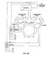
- FIG. 2is a schematic cross-sectional view of a PECVD chamber configured for performing the processes according to the present invention.
- FIG. 2 ais a schematic diagram of a gas box system for supplying gases to the PECVD chamber 200 of FIG. 2 .
- FIG. 3is a graph comparing the amount of Al consumed by MOCVD TiN and PECVD TiN.
- FIG. 4is an integrated multi-chamber processing apparatus configured for sequential metallization in accordance with the present invention.
- the present inventionprovides a method and an apparatus for improved metallization of apertures to form continuous, void-free interconnections with reduced resistivity and greater effective line width, including contacts or vias in high aspect ratio sub-half micron applications.
- One aspect of the inventionprovides a method for metallizing apertures where a refractory metal layer is deposited onto a substrate having high aspect ratio apertures formed thereon.
- a PECVD refractory metal nitride layeris formed on the refractory metal layer such as described in more detail below.
- a metal layeris deposited over the metal nitride layer.
- the processis preferably carried out in an integrated processing system that includes various chambers so that once the substrate is introduced into a vacuum environment, the metallization of the vias and contacts occurs without exposure to possible atmospheric contaminants.
- TiN barrier/wetting layerat elevated temperatures (e.g. at 450° Celsius) readily decomposes and interacts with an adjacent metal layer, such as an Al metal layer to form TiAl x (where x is a counting number).
- the TiAl xdiffuses into the Al layer which causes the Al to have a higher resistivity.
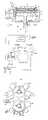
- TiAl x formation 100further reduces the linewidth 101 of the feature when Al is deposited on a Ti layer 102 /TiN layer 103 .
- TiAl x 100forms over the TiN layer 103 on the sidewalls 104 of the aperture 105 causing significant linewidth reduction 106 .
- the present inventioninvolves an improved method of depositing a metal nitride barrier/wetting layer which releases less impurities and has less interactions with the metal layer.
- the improved method of forming a PECVD metal nitride layer on a substratecomprises injecting a mixture of a metal-containing compound, a nitrogen-containing gas, and a hydrogen-containing gas in a chamber; and generating a plasma from the mixture to deposit a metal nitride layer on the substrate.
- a plasmais established from a mixture which includes a hydrogen-containing gas during the metal nitride deposition step because the hydrogen atoms, in its excited energy state, is reactive enough to scavenge the impurities in the metal nitride deposition process.
- the metal nitride filmis preferably TiN.
- the metal-containing compound usedis preferably tetrakis-dimethylamino-titanium (TDMAT) precursor gas. Carbon impurities exist in the reaction of a metallo-organic TDMAT precursor gas to form a TiN layer.
- Using hydrogen plasma in the deposition stepresults in a metal nitride layer that releases less impurities, and, thus, results in a metal nitride layer which decomposes less rapidly at high temperatures and reacts less with a metal layer that is applied to it. Furthermore, a cleaner metal nitride layer means that fewer impurities diffuse through the layer to react with the above metal layer.
- a PECVD TiN filmhas a resistivity that is reduced by about a factor of 5 when compared to a metallo-organic CVD TiN film.
- Using hydrogen plasma in the deposition stepis preferable to using hydrogen plasma to post treat a deposited metal nitride film.
- the effect of the hydrogen plasmais reduced because the carbon impurities are already formed in themetal nitride film.
- Another advantage of using hydrogen plasma during the deposition stepis that the plasma also in situ cleans the chamber. Thus, the throughput of processing the substrate is increased as a result of less time needed to clean the chamber.
- the process of forming a PECVD metal nitride filmis also advantageous because the resulting film has a poly-crystalline structure whereas a MOCVD metal nitride film has an amorphous structure.
- a poly-crystalline structurethe metal and nitrogen bonds are stronger than in an amorphous structure.
- the metal nitridecreates a better barrier layer to a metal layer that is applied over it.
- using a PECVD metal nitride layer, rather than a MOCVD metal nitride layerresults in greater effective line width for apertures because a PECVD metal nitride forms a thinner layer on the sidewalls of apertures.
- the process of depositing a metal nitride filmcan also comprise the step of treating the metal nitride film with nitrogen plasma.
- the nitrogen plasmaimproves the microstructure of the metal nitride film because both PECVD and MOCVD metal nitride films are not sufficiently densified during the deposition step.
- a nitrogen plasma treatmentreduces the resistivity of a PECVD TiN film by about a factor of 10 when compared to a metallo-organic CVD TiN film and by about a factor of 2 when compared to a PECVD TiN film without a nitrogen plasma treatment.
- the densified metal nitride filmis also a better barrier because the denser film prevents the diffusion of metals through the metal nitride film.
- the process of depositing a metal nitride filmcan further comprise pretreating the substrate with argon plasma before deposition of the metal nitride. Pretreating the substrate with argon plasma expels any contaminants on the surface of the substrate when the substrate was exposed to atmospheric conditions.
- FIG. 2illustrates a schematic cross-sectional view of an example of a PECVD chamber suitable for performing the process of the present invention.
- This specific reactor, a TxZ chamber 200is available commercially from Applied Materials, Inc., of Santa Clara, Calif. Details of this chamber have been disclosed in commonly-assigned U.S. Pat. No. 5,846,332, entitled “Thermally Floating Pedestal Collar in a Chemical Vapor Deposition Chamber”, issued Dec. 8, 1998, and commonly-assigned U.S. Pat. No. 5,993,916, entitled “Method for Substrate Processing with Improved Throughput and Yield”, issued Nov. 30, 1999, both which are incorporated herein by reference.
- the TxZ chamber 200is adapted for operation in a reduced pressure environment through connection to a vacuum pump 280 via a pumping channel 208 .
- the chamber 200comprises a chamber body 202 and a pedestal 204 that supports a substrate 290 to be processed.
- the substrate 290is transferred in and out of the chamber 200 through a slit valve 206 , and is centered upon the pedestal 204 by a centering ring 212 .
- a suitable robotics transfer assemblyis described in commonly-assigned U.S. Pat. No. 4,951,601, entitled “Multi-chamber Integrated Process System” issued on Aug. 28, 1990, the complete disclosure of which is incorporated herein by reference.
- the substrate 290is placed in close proximity to a gas distribution faceplate, or a showerhead 240 , which includes a larger number of passageways 242 to allow the flow of a process gas from a gas inlet 244 into a processing zone 250 inside the chamber 200 .
- Film depositionoccurs on the surface of the substrate 290 when the process gas reacts at the substrate 290 . Any excess process gas and byproducts are subsequently pumped out of the chamber 200 through an annular pumping channel 208 , which is connected to a pumping plenum 270 .
- the PECVD chamber 200includes an electrical power source 214 which supplies power to a resistive heater 205 of the pedestal 204 .
- the pedestal 204and thus the substrate 290 , can be maintained at an elevated temperature.
- the PECVD chamberalso includes a RF source 216 which provides RF power which is applied to the showerhead 240 , which acts as an upper electrode.
- the showerhead 240is electrically insulated from the rest of the chamber 200 by the annular isolator ring 264 , typically made of an electrically non-conductive ceramic. Sufficient voltage and power is applied by the RF source 216 to generate a plasma from the process gases within the processing region 250 .
- the chamber 200is designed to minimize undesirable deposition upon various chamber components—e.g., the centering ring 212 is maintained at a lower temperature than the pedestal 204 , such that film deposition on the centering ring can be minimized.
- a mixture of a metal-containing compoundlike TDMAT
- a nitrogen-containing gasand a hydrogen gas is injected into the chamber 200 through the showerhead 240 .
- the metal-containing compoundcan be introduced through the showerhead 240 by bubbling a carrier gas, such as helium, through a liquid sample of the metal-containing compound contained in an ampoule or bubbler (not shown).
- a direct liquid injection systemmay also be used to introduce the metal-containing compound into the chamber 200 .
- a plasmais generated from the mixture when power is applied to the RF source 216 .
- the power level applied to the RF source 216is preferably 350 to 1000 watts, and most preferably at 750 watts.
- the mixturepreferably comprises a molar ratio from the range of 5:1 to 1:1 of hydrogen to nitrogen.
- the mixturemost preferably comprises a molar ratio of about 4 to 1 hydrogen to nitrogen.
- the nitrogen-containing gasis nitrogen gas and the hydrogen-containing gas is hydrogen gas. If nitrogen gas and hydrogen gas are used, the gases are preferably injected at a flow rate of the hydrogen gas at 200 sccm and the a flow rate of the nitrogen gas at 50 sccm.
- FIG. 2 ais a schematic diagram of a gas box system for supplying gases to the PECVD chamber 200 in FIG. 2 . When PECVD TiN is to be used, the gas box is supplied with N 2 , H 2 , He, and Ar.
- the reactant TDMAT along with the inert gas Heis passed into the chamber 200 for processing.
- the substrate 290is heated from the pedestal 204 which is set at a temperature in a range that is preferably from about 350° C. to about 500° C.
- the substrateis preferably heated to a temperature in a range that is preferably from about 300° C. to about 450° C.
- the heater spacingis set at a distance of about 250 mils to about 500 mils, and preferably at 300 mils.
- the chamber pressureis maintained at a pressure from about 1 torr to about 10 torr, and preferably at about 3 torr.
- the thickness of the metal nitridedepends on the intended use of the metal nitride.
- the preferable thicknessis from about 10 angstroms to about 200 angstroms with a thickness of 50 angstroms most preferred.
- the metal nitride filmis treated with a nitrogen plasma.
- a nitrogen gasis introduced into the chamber 200 through the showerhead 240 .
- a plasmais generated from the nitrogen gas when power is applied to the RF source 216 .
- the power level applied to the RF source 216is preferably 350 to 1000 watts, and most preferably at 750 watts.
- the substrate 290is heated to a temperature that is preferably about 350° C. to about 500° C.
- the chamber pressureis maintained at a pressure that is preferably from about 1 torr to 5 torr, and most preferably at 1.5 torr.
- the substrateis treated with the nitrogen plasma for a time period that is preferably from about 20 seconds to about 70 seconds, and most preferably for about 35 seconds.
- the present inventionfurther provides a method of forming a feature on a substrate comprising the steps of depositing a refractory metal layer over the surface of an aperture, depositing a PECVD refractory metal nitride layer over the surface of the refractory metal layer, and depositing a metal layer over the refractory metal nitride layer.
- the present inventioninterposes the barrier/wetting layer between a metal layer and the dielectric to improve the wetting of the metal.
- An appropriate barrier/wetting layeris one that wets the metal better than the dielectric material. It is preferred that the barrier/wetting layer provide improved wetting even when only a thin barrier/wetting layer is deposited. It follows that a preferred barrier/wetting layer is formed substantially uniformly over the surface of the dielectric, including the walls and floors of apertures.
- the barrier/wetting layercomprises a refractory metal layer formed over the dielectric layer and then the PECVD metal nitride layer formed over the refractory metal layer.
- the underlying refractory metal layeris preferably Ti but can also include, but is not limited to, Tantalum (Ta), tungsten (W), niobium (Nb), cobalt (Co), and molybdenum (Mo).
- the refractory metal layercan be deposited by either PVD or CVD processes.
- the metal nitride layeris formed by PECVD over the refractory metal layer. The PECVD processes of the present invention have been discussed above.
- the metal nitride layeris preferably TiN.
- the preferred barrier/wetting layeris a Ti/TiN layer but the barrier/wetting layer can comprise of any of the above combinations of refractory metal layers and metal nitride layers.
- a metal layeris deposited on the barrier/wetting layer.
- Metal features formed in semiconductor devicessuch as plugs and lines formed in vias and trenches, are typically made of Al.
- Cu and Wcan also be used.
- a Ti/TiN layercannot be used as a barrier to a Cu metal layer because the Cu diffuses through the layer. Diffusion of Cu to the adjacent dielectric material can cause electrical shorts to occur.
- Cucan be used over the Ti/TiN layer of the present invention because the PECVD TiN film is a denser than a MOCVD TiN film and acts as a sufficient barrier to prevent Cu diffusion through PECVD TiN film.
- the metal layeris deposited first by a CVD metal conformal wetting layer applied over the barrier/wetting layer without sealing the top of the vias. Then a PVD metal layer is deposited thereon.
- the metal layercan be deposited by just a PVD step.
- the metal layercan be deposited by depositing a seed metal layer over the metal nitride layer and then electroplating a metal layer over the seed metal layer.
- the resulting metal layer applied over a barrier/wetting layeris substantially void free, has reduced resistivity, and has greater effective line width.
- PECVD TiNis a better barrier between the underlying refractory metal layer and the metal layer above.
- FIG. 3compares the reactivity of 100 ⁇ as dep TiN, 1 ⁇ 50 ⁇ TiN, PECVD TiN, and nitrogen-plasma-treated PECVD TiN with Al upon annealing at 450° C. in a nitrogen gas furnace for 30 minutes. For each case, 1000 ⁇ of Al is deposited on the TiN and the amount of Al consumed is calculated.
- PECVD TiNconsumes less of the Al layer formed over the metal nitride layer.
- PECVD TiNreduces the amount of Al consumed by 30%. With less Al consumption and less TiAl x formation, the Al feature has a greater effective linewidth and a lower resistivity because of less TiAl x diffusion into the Al layer.
- Electron micrographsshow complete fill for low temperature integrated Al metallization of an aperture with PECVD TiN as liner material with thicknesses of 0.25 um, 0.35 um, and 0.45 um. Complete fill was demonstrated for a film stack made up of 200 ⁇ of IMP Ti, about 100 ⁇ of nitrogen-plasma-treated PECVD TiN, 600 ⁇ of CVD Al, and 10 k ⁇ of PVD Al. PVD Al was deposited at a temperature of about 400° C. Electron micrographs also confirm the good step coverage of PECVD TiN on apertures of 0.25 um, 0.35 um, and 0.45 um.
- the process of forming a feature on a substratecan be performed in either a multi-chamber processing apparatus (e.g., a cluster tool) having PECVD, CVD, and PVD chambers, or separate single-chamber systems.
- a multi-chamber processing apparatuse.g., a cluster tool
- the use of a multi-chamber apparatusis preferred because the substrate can be kept within a vacuum environment to prevent contamination between processing steps.
- FIG. 4depicts a schematic illustration of a multi-chamber process apparatus 400 , an Endura system commercially available from Applied Materials, Inc., Santa Clara, Calif.
- a similar staged-vacuum wafer processing systemis disclosed in U.S. Pat. No. 5,186,718 entitled “Staged-Vacuum Wafer Processing System and Method” issued to Tepman et al. on Feb. 16, 1993, which is herein incorporated by reference.
- a microprocessor controller 401is provided to control the sequence and formation of the desired film layers on the substrates.
- the cluster toolgenerally includes a de-gas chamber 402 wherein the substrates are introduced to outgas contaminants.
- the substrateis then moved into a pre-clean chamber 403 where the surface of the substrate is cleaned.
- the substrateis moved by the robot into a chamber 405 to deposit a metal refractory layer like a CVD or PVD chamber.
- the substrateis moved into a chamber 406 to deposit a PECVD metal nitride.
- the apparatusfurther comprises a hydrogen gas source in communication with the metal nitride chamber.
- the substrateis moved into a CVD metal chamber 407 .
- the substrateis processed in PVD metal chamber 408 .
- the substratecan be further processed in a PVD TiN anti-reflection coating (“ARC”) chamber 409 for reducing the reflectivity of the surface and improving the photolithographic performance of the layer.
- ARCPVD TiN anti-reflection coating
- the chamberstypically include an enclosure, a substrate support member located within the enclosure and means for providing deposition material to be deposited on the substrates, and power means to provide an electrical bias within the chambers.
- the cluster toolalso generally includes two robots for transferring the substrate through the processing steps required for the formation of film layers thereon.
- the processes of the present inventioncan be implemented using a computer program product that runs on a conventional computer system comprising a central processor unit (CPU) interconnected to a memory system with peripheral control components, such as for example a 68400 microprocessor, commercially available from Synenergy Microsystems, California.
- the computer program codecan be written in any conventional computer readable programming language such as for example 68000 assembly language, C, C++, or Pascal. Suitable program code is entered into a single file, or multiple files, using a conventional text editor, and stored or embodied in a computer usable medium, such as a memory system of the computer. If the entered code text is in a high level language, the code is compiled, and the resultant compiler code is then linked with an object code of precompiled windows library routines.
- the system userinvokes the object code, causing the computer system to load the code in memory, from which the CPU reads and executes the code to perform the tasks identified in the program.
- a suitable hierarchical control structure of the present computer programis disclosed in United States patent application with an application Ser. No. 08/792,292, which is herein incorporated by reference.
Landscapes
- Chemical & Material Sciences (AREA)
- Engineering & Computer Science (AREA)
- General Chemical & Material Sciences (AREA)
- Chemical Kinetics & Catalysis (AREA)
- Manufacturing & Machinery (AREA)
- Computer Hardware Design (AREA)
- Microelectronics & Electronic Packaging (AREA)
- Power Engineering (AREA)
- Physics & Mathematics (AREA)
- General Physics & Mathematics (AREA)
- Condensed Matter Physics & Semiconductors (AREA)
- Inorganic Chemistry (AREA)
- Materials Engineering (AREA)
- Mechanical Engineering (AREA)
- Metallurgy (AREA)
- Organic Chemistry (AREA)
- Internal Circuitry In Semiconductor Integrated Circuit Devices (AREA)
- Chemical Vapour Deposition (AREA)
- Electrodes Of Semiconductors (AREA)
Abstract
Description
1. Field of the Invention
The present invention relates to the metallization of apertures to form void-free interconnections, including contacts or vias in high aspect ratio sub-half micron applications. More particularly, the present invention relates to a new metal nitride deposition process and apparatus.
2. Background of the Related Art
Sub-half micron multilevel metallization is one of the key technologies for the next generation of very large scale integration (“VLSI”). The multilevel interconnections that lie at the heart of the technology require planarization of high aspect ratio apertures, including contacts, vias, lines, or other features. Reliable formation of these interconnects is very important to the success of VLSI and to the continued effort to increase circuit density and quality of individual substrates and dies.
Physical vapor deposition (“PVD”) of aluminum (Al) or copper (Cu) is a common method to fill apertures. However, a problem with the PVD Al layer is the formation of voids which occur through a key hole process wherein the top portion of the via becomes sealed before the via has been entirely filled. As a consequence, as disclosed in U.S. Pat. No. 5,877,087 entitled “Low temperature integrated metallization process and apparatus” issued to Mosely et al. on Mar. 2, 1999 and as disclosed in its divisional United States patent application with an application Ser. No. 08/792,292 which are both incorporated herein by reference, a low temperature integrated metallization process has been developed to form void-free contacts or vias. The process comprises depositing a thin glue layer comprising a refractory metal. Possible glue layers include, but is not limited to, a titanium (Ti) and a titanium nitride (TiN) layer or a tantalum (Ta) and a tantalum nitride (TaN) layer. After the glue layer a conformal wetting layer of chemical vapor deposition (CVD) Al (or CVD Cu) is formed at low temperatures over the glue layer for the receipt of a layer of physical vapor deposition (“PVD”) Al (or PVD Cu) thereon. Then, a PVD Al (or PVD Cu) layer is deposited onto the previously formed CVD Al (or CVD Cu) layer at a temperature below that of the melting point temperature of Al (or Cu). This low temperature integrated metallization process results in a CVD/PVD Al (or Cu) layer that is substantially void-free.
However, a problem with this low temperature integrated metallization process is that high wiring resistance is found for features of dimensions less than 0.2 um. The high wiring resistance problem arises mainly with integrated circuit applications where sintering at 450° Celsius for 30 minutes is performed upon completion of all process steps to repair any damage to the capacitors. There are three major causes of the high wiring resistance problem. First, the Ti/TiN layer readily decomposes and interacts at elevated temperatures (e.g. at 450° Celsius) with an adjacent metal such as Al to form TiAlx. As a result of TiAlxformation on the sidewalls of apertures, the effective linewidth of the feature is reduced. Second, the TiN layer formed by metallo-organic chemical vapor deposition usually contains certain levels of impurities. At elevated temperatures, the impurities easily diffuse into the adjacent metal, which results in high resistivity. Third, the chemical vapor deposition of TiN using metallo-organic precusors forms a relatively thick layer of TiN on the sidewalls of apertures. This effectively reduces the line width of metal lines, especially for very thin lines.
Therefore, there is a need for a metallization process for creating line features that are void-free, have low resistivity, and greater effective line width. More particularly, it would be desirable to have a low temperature process for filling such contacts and vias with a glue layer and a metal layer where the glue layer does not react with the metal layer to form impurities, has fewer impurities that diffuse into the metal layer, and has less sidewall coverage of apertures.
The present invention generally provides improved metallization of apertures to form continuous, void-free interconnections with reduced resistivity and greater effective line width, including contacts or vias in high aspect ratio sub-half micron applications. More particularly, the present invention provides a low temperature process for filling such apertures with a glue layer and a metal layer where the glue layer does not react with the metal layer to form impurities, has fewer impurities that diffuse into the metal layer, and has less sidewall coverage of the apertures.
In one aspect of the invention, a refractory metal layer is deposited onto a substrate having high aspect ratio contacts or vias formed thereon. Next, a plasma-enhanced CVD (PECVD) refractory metal nitride layer is deposited on the refractory metal layer. Then, a metal layer is deposited over the metal nitride layer. PECVD of the metal nitride layer comprises contacting a plasma of a metal precursor gas, a nitrogen-containing gas, and a hydrogen-containing gas with the substrate to form a metal nitride layer. The deposited metal nitride layer is preferably treated with nitrogen plasma to densify the metal nitride film. The present invention reduces the interaction between the metal nitride layer and the metal layer at high temperatures because the PECVD metal nitride layer releases less impurities and has better microstructure compared to a metal nitride layer deposited by MOCVD. In addition, the metal layer has a lower resistivity because of the improved metal nitride layer. The resulting metal layer is substantially void free, has reduced resistivity, and has greater effective line width.
The present invention further provides an apparatus for providing improved step coverage and planarization of metal layers. The apparatus comprises an integrated processing system that generally includes various chambers so that once the substrate is introduced into a vacuum environment, the metallization of the vias and contacts occurs without exposure to possible contaminants.
So that the manner in which the above recited features, advantages and objects of the present invention are attained and can be understood in detail, a more particular description of the invention, briefly summarized above, may be had by reference to the embodiments thereof which are illustrated in the appended drawings.
It is to be noted, however, that the appended drawings illustrate only typical embodiments of this invention and are therefore not to be considered limiting of its scope, for the invention may admit to other equally effective embodiments.
FIG. 1 is a schematic cross-section diagram of the prior art of the effective wiring line width of an aperture.
FIG. 2 is a schematic cross-sectional view of a PECVD chamber configured for performing the processes according to the present invention.
FIG. 2ais a schematic diagram of a gas box system for supplying gases to thePECVD chamber 200 of FIG.2.
FIG. 3 is a graph comparing the amount of Al consumed by MOCVD TiN and PECVD TiN.
FIG. 4 is an integrated multi-chamber processing apparatus configured for sequential metallization in accordance with the present invention.
The present invention provides a method and an apparatus for improved metallization of apertures to form continuous, void-free interconnections with reduced resistivity and greater effective line width, including contacts or vias in high aspect ratio sub-half micron applications. One aspect of the invention provides a method for metallizing apertures where a refractory metal layer is deposited onto a substrate having high aspect ratio apertures formed thereon. Next, a PECVD refractory metal nitride layer is formed on the refractory metal layer such as described in more detail below. Then, a metal layer is deposited over the metal nitride layer. The process is preferably carried out in an integrated processing system that includes various chambers so that once the substrate is introduced into a vacuum environment, the metallization of the vias and contacts occurs without exposure to possible atmospheric contaminants.
The current low temperature integrated metallization process of depositing a metal layer over a barrier/wetting layer suffers from the problem of high metal resistivity. One of the reasons this problem occurs is that a TiN barrier/wetting layer at elevated temperatures (e.g. at 450° Celsius) readily decomposes and interacts with an adjacent metal layer, such as an Al metal layer to form TiAlx(where x is a counting number). The TiAlxdiffuses into the Al layer which causes the Al to have a higher resistivity. In addition, as shown in FIG. 1, TiAlxformation 100 further reduces thelinewidth 101 of the feature when Al is deposited on aTi layer 102/TiN layer 103. TiAlx100 forms over theTiN layer 103 on thesidewalls 104 of theaperture 105 causingsignificant linewidth reduction 106.
The present invention involves an improved method of depositing a metal nitride barrier/wetting layer which releases less impurities and has less interactions with the metal layer. The improved method of forming a PECVD metal nitride layer on a substrate comprises injecting a mixture of a metal-containing compound, a nitrogen-containing gas, and a hydrogen-containing gas in a chamber; and generating a plasma from the mixture to deposit a metal nitride layer on the substrate.
A plasma is established from a mixture which includes a hydrogen-containing gas during the metal nitride deposition step because the hydrogen atoms, in its excited energy state, is reactive enough to scavenge the impurities in the metal nitride deposition process. The metal nitride film is preferably TiN. In depositing TiN, the metal-containing compound used is preferably tetrakis-dimethylamino-titanium (TDMAT) precursor gas. Carbon impurities exist in the reaction of a metallo-organic TDMAT precursor gas to form a TiN layer. Using hydrogen plasma in the deposition step results in a metal nitride layer that releases less impurities, and, thus, results in a metal nitride layer which decomposes less rapidly at high temperatures and reacts less with a metal layer that is applied to it. Furthermore, a cleaner metal nitride layer means that fewer impurities diffuse through the layer to react with the above metal layer. In addition, a PECVD TiN film has a resistivity that is reduced by about a factor of 5 when compared to a metallo-organic CVD TiN film.
Using hydrogen plasma in the deposition step is preferable to using hydrogen plasma to post treat a deposited metal nitride film. In post-treating a metal nitride film, the effect of the hydrogen plasma is reduced because the carbon impurities are already formed in themetal nitride film. Another advantage of using hydrogen plasma during the deposition step is that the plasma also in situ cleans the chamber. Thus, the throughput of processing the substrate is increased as a result of less time needed to clean the chamber.
The process of forming a PECVD metal nitride film is also advantageous because the resulting film has a poly-crystalline structure whereas a MOCVD metal nitride film has an amorphous structure. In a poly-crystalline structure, the metal and nitrogen bonds are stronger than in an amorphous structure. Thus, the metal nitride creates a better barrier layer to a metal layer that is applied over it. Furthermore, using a PECVD metal nitride layer, rather than a MOCVD metal nitride layer, results in greater effective line width for apertures because a PECVD metal nitride forms a thinner layer on the sidewalls of apertures.
The process of depositing a metal nitride film can also comprise the step of treating the metal nitride film with nitrogen plasma. The nitrogen plasma improves the microstructure of the metal nitride film because both PECVD and MOCVD metal nitride films are not sufficiently densified during the deposition step. A nitrogen plasma treatment reduces the resistivity of a PECVD TiN film by about a factor of 10 when compared to a metallo-organic CVD TiN film and by about a factor of 2 when compared to a PECVD TiN film without a nitrogen plasma treatment. The densified metal nitride film is also a better barrier because the denser film prevents the diffusion of metals through the metal nitride film. In addition, the process of depositing a metal nitride film can further comprise pretreating the substrate with argon plasma before deposition of the metal nitride. Pretreating the substrate with argon plasma expels any contaminants on the surface of the substrate when the substrate was exposed to atmospheric conditions.
FIG. 2 illustrates a schematic cross-sectional view of an example of a PECVD chamber suitable for performing the process of the present invention. This specific reactor, aTxZ chamber 200, is available commercially from Applied Materials, Inc., of Santa Clara, Calif. Details of this chamber have been disclosed in commonly-assigned U.S. Pat. No. 5,846,332, entitled “Thermally Floating Pedestal Collar in a Chemical Vapor Deposition Chamber”, issued Dec. 8, 1998, and commonly-assigned U.S. Pat. No. 5,993,916, entitled “Method for Substrate Processing with Improved Throughput and Yield”, issued Nov. 30, 1999, both which are incorporated herein by reference. TheTxZ chamber 200 is adapted for operation in a reduced pressure environment through connection to avacuum pump 280 via apumping channel 208. Thechamber 200 comprises achamber body 202 and apedestal 204 that supports asubstrate 290 to be processed. Thesubstrate 290 is transferred in and out of thechamber 200 through aslit valve 206, and is centered upon thepedestal 204 by a centeringring 212. A suitable robotics transfer assembly is described in commonly-assigned U.S. Pat. No. 4,951,601, entitled “Multi-chamber Integrated Process System” issued on Aug. 28, 1990, the complete disclosure of which is incorporated herein by reference.
During processing, thesubstrate 290 is placed in close proximity to a gas distribution faceplate, or ashowerhead 240, which includes a larger number ofpassageways 242 to allow the flow of a process gas from agas inlet 244 into aprocessing zone 250 inside thechamber 200. Film deposition occurs on the surface of thesubstrate 290 when the process gas reacts at thesubstrate 290. Any excess process gas and byproducts are subsequently pumped out of thechamber 200 through anannular pumping channel 208, which is connected to apumping plenum 270.
ThePECVD chamber 200 includes anelectrical power source 214 which supplies power to aresistive heater 205 of thepedestal 204. Thepedestal 204, and thus thesubstrate 290, can be maintained at an elevated temperature. The PECVD chamber also includes aRF source 216 which provides RF power which is applied to theshowerhead 240, which acts as an upper electrode. Theshowerhead 240 is electrically insulated from the rest of thechamber 200 by theannular isolator ring 264, typically made of an electrically non-conductive ceramic. Sufficient voltage and power is applied by theRF source 216 to generate a plasma from the process gases within theprocessing region 250. Thechamber 200 is designed to minimize undesirable deposition upon various chamber components—e.g., the centeringring 212 is maintained at a lower temperature than thepedestal 204, such that film deposition on the centering ring can be minimized.
In the preferred process of depositing a metal nitride, a mixture of a metal-containing compound (like TDMAT), a nitrogen-containing gas, and a hydrogen gas is injected into thechamber 200 through theshowerhead 240. The metal-containing compound can be introduced through theshowerhead 240 by bubbling a carrier gas, such as helium, through a liquid sample of the metal-containing compound contained in an ampoule or bubbler (not shown). Alternatively, a direct liquid injection system may also be used to introduce the metal-containing compound into thechamber 200. A plasma is generated from the mixture when power is applied to theRF source 216. The power level applied to theRF source 216 is preferably 350 to 1000 watts, and most preferably at 750 watts. The mixture preferably comprises a molar ratio from the range of 5:1 to 1:1 of hydrogen to nitrogen. The mixture most preferably comprises a molar ratio of about 4 to 1 hydrogen to nitrogen. Preferably, the nitrogen-containing gas is nitrogen gas and the hydrogen-containing gas is hydrogen gas. If nitrogen gas and hydrogen gas are used, the gases are preferably injected at a flow rate of the hydrogen gas at 200 sccm and the a flow rate of the nitrogen gas at 50 sccm. FIG. 2ais a schematic diagram of a gas box system for supplying gases to thePECVD chamber 200 in FIG.2. When PECVD TiN is to be used, the gas box is supplied with N2, H2, He, and Ar. The reactant TDMAT along with the inert gas He is passed into thechamber 200 for processing. Thesubstrate 290 is heated from thepedestal 204 which is set at a temperature in a range that is preferably from about 350° C. to about 500° C. The substrate is preferably heated to a temperature in a range that is preferably from about 300° C. to about 450° C. The heater spacing is set at a distance of about 250 mils to about 500 mils, and preferably at 300 mils. The chamber pressure is maintained at a pressure from about 1 torr to about 10 torr, and preferably at about 3 torr. The thickness of the metal nitride depends on the intended use of the metal nitride. However, the preferable thickness is from about 10 angstroms to about 200 angstroms with a thickness of 50 angstroms most preferred. After deposition of the metal nitride on thesubstrate 290, the metal nitride film is treated with a nitrogen plasma. A nitrogen gas is introduced into thechamber 200 through theshowerhead 240. A plasma is generated from the nitrogen gas when power is applied to theRF source 216. The power level applied to theRF source 216 is preferably 350 to 1000 watts, and most preferably at 750 watts. Thesubstrate 290 is heated to a temperature that is preferably about 350° C. to about 500° C. The chamber pressure is maintained at a pressure that is preferably from about 1 torr to 5 torr, and most preferably at 1.5 torr. The substrate is treated with the nitrogen plasma for a time period that is preferably from about 20 seconds to about 70 seconds, and most preferably for about 35 seconds.
The present invention further provides a method of forming a feature on a substrate comprising the steps of depositing a refractory metal layer over the surface of an aperture, depositing a PECVD refractory metal nitride layer over the surface of the refractory metal layer, and depositing a metal layer over the refractory metal nitride layer.
It has been demonstrated that some soft metals, such as Al and Cu can flow at temperatures below their respective melting points due to the effects of surface tension. However, these metals have a tendency to dewet from an underlying dielectric layer at high temperatures. Therefore, the present invention interposes the barrier/wetting layer between a metal layer and the dielectric to improve the wetting of the metal. An appropriate barrier/wetting layer is one that wets the metal better than the dielectric material. It is preferred that the barrier/wetting layer provide improved wetting even when only a thin barrier/wetting layer is deposited. It follows that a preferred barrier/wetting layer is formed substantially uniformly over the surface of the dielectric, including the walls and floors of apertures.
According to the present invention, the barrier/wetting layer comprises a refractory metal layer formed over the dielectric layer and then the PECVD metal nitride layer formed over the refractory metal layer. The underlying refractory metal layer is preferably Ti but can also include, but is not limited to, Tantalum (Ta), tungsten (W), niobium (Nb), cobalt (Co), and molybdenum (Mo). The refractory metal layer can be deposited by either PVD or CVD processes. The metal nitride layer is formed by PECVD over the refractory metal layer. The PECVD processes of the present invention have been discussed above. The metal nitride layer is preferably TiN. The preferred barrier/wetting layer is a Ti/TiN layer but the barrier/wetting layer can comprise of any of the above combinations of refractory metal layers and metal nitride layers.
Next, a metal layer is deposited on the barrier/wetting layer. Metal features formed in semiconductor devices, such as plugs and lines formed in vias and trenches, are typically made of Al. However, Cu and W can also be used. Normally, a Ti/TiN layer cannot be used as a barrier to a Cu metal layer because the Cu diffuses through the layer. Diffusion of Cu to the adjacent dielectric material can cause electrical shorts to occur. Cu can be used over the Ti/TiN layer of the present invention because the PECVD TiN film is a denser than a MOCVD TiN film and acts as a sufficient barrier to prevent Cu diffusion through PECVD TiN film. Preferably, the metal layer is deposited first by a CVD metal conformal wetting layer applied over the barrier/wetting layer without sealing the top of the vias. Then a PVD metal layer is deposited thereon. Alternatively, the metal layer can be deposited by just a PVD step. Still another alternative is that the metal layer can be deposited by depositing a seed metal layer over the metal nitride layer and then electroplating a metal layer over the seed metal layer.
The resulting metal layer applied over a barrier/wetting layer is substantially void free, has reduced resistivity, and has greater effective line width. As shown in FIG. 3, PECVD TiN is a better barrier between the underlying refractory metal layer and the metal layer above. FIG. 3 compares the reactivity of 100 Å as dep TiN, 1×50 Å TiN, PECVD TiN, and nitrogen-plasma-treated PECVD TiN with Al upon annealing at 450° C. in a nitrogen gas furnace for 30 minutes. For each case, 1000 Å of Al is deposited on the TiN and the amount of Al consumed is calculated. FIG. 3 shows that both PECVD TiN and nitrogen-plasma-treated PECVD TiN consume less of the Al layer formed over the metal nitride layer. PECVD TiN reduces the amount of Al consumed by 30%. With less Al consumption and less TiAlxformation, the Al feature has a greater effective linewidth and a lower resistivity because of less TiAlxdiffusion into the Al layer.
Using a PECVD metal nitride liner does not compromise the low temperature integrated metallization process. Electron micrographs show complete fill for low temperature integrated Al metallization of an aperture with PECVD TiN as liner material with thicknesses of 0.25 um, 0.35 um, and 0.45 um. Complete fill was demonstrated for a film stack made up of 200 Å of IMP Ti, about 100 Å of nitrogen-plasma-treated PECVD TiN, 600 Å of CVD Al, and 10 kÅ of PVD Al. PVD Al was deposited at a temperature of about 400° C. Electron micrographs also confirm the good step coverage of PECVD TiN on apertures of 0.25 um, 0.35 um, and 0.45 um.
The process of forming a feature on a substrate can be performed in either a multi-chamber processing apparatus (e.g., a cluster tool) having PECVD, CVD, and PVD chambers, or separate single-chamber systems. The use of a multi-chamber apparatus is preferred because the substrate can be kept within a vacuum environment to prevent contamination between processing steps.
FIG. 4 depicts a schematic illustration of amulti-chamber process apparatus 400, an Endura system commercially available from Applied Materials, Inc., Santa Clara, Calif. A similar staged-vacuum wafer processing system is disclosed in U.S. Pat. No. 5,186,718 entitled “Staged-Vacuum Wafer Processing System and Method” issued to Tepman et al. on Feb. 16, 1993, which is herein incorporated by reference.
Amicroprocessor controller 401 is provided to control the sequence and formation of the desired film layers on the substrates. The cluster tool generally includes ade-gas chamber 402 wherein the substrates are introduced to outgas contaminants. The substrate is then moved into apre-clean chamber 403 where the surface of the substrate is cleaned. Depending on the particular application, the substrate is moved by the robot into achamber 405 to deposit a metal refractory layer like a CVD or PVD chamber. Next, the substrate is moved into achamber 406 to deposit a PECVD metal nitride. The apparatus further comprises a hydrogen gas source in communication with the metal nitride chamber. Following deposition of the PECVD metal nitride, the substrate is moved into aCVD metal chamber 407. Next, the substrate is processed inPVD metal chamber 408. The substrate can be further processed in a PVD TiN anti-reflection coating (“ARC”)chamber 409 for reducing the reflectivity of the surface and improving the photolithographic performance of the layer.
It should be appreciated that one of ordinary skill in the art would appreciate the structure and operation of the chambers shown in FIG.4. Generally, the chambers typically include an enclosure, a substrate support member located within the enclosure and means for providing deposition material to be deposited on the substrates, and power means to provide an electrical bias within the chambers. The cluster tool also generally includes two robots for transferring the substrate through the processing steps required for the formation of film layers thereon.
The processes of the present invention can be implemented using a computer program product that runs on a conventional computer system comprising a central processor unit (CPU) interconnected to a memory system with peripheral control components, such as for example a 68400 microprocessor, commercially available from Synenergy Microsystems, California. The computer program code can be written in any conventional computer readable programming language such as for example 68000 assembly language, C, C++, or Pascal. Suitable program code is entered into a single file, or multiple files, using a conventional text editor, and stored or embodied in a computer usable medium, such as a memory system of the computer. If the entered code text is in a high level language, the code is compiled, and the resultant compiler code is then linked with an object code of precompiled windows library routines. To execute the linked compiled object code, the system user invokes the object code, causing the computer system to load the code in memory, from which the CPU reads and executes the code to perform the tasks identified in the program. A suitable hierarchical control structure of the present computer program is disclosed in United States patent application with an application Ser. No. 08/792,292, which is herein incorporated by reference.
While the foregoing is directed to the preferred embodiment of the present invention, other and further embodiments of the invention may be devised without departing from the basic scope thereof, and the scope thereof is determined by the claims that follow.
Claims (28)
1. A method of depositing a titanium nitride film on a substrate, comprising:
(a) injecting a mixture of a titanium metallo-organic precursor compound, nitrogen gas, and hydrogen gas in a chamber;
(b) generating a plasma from the mixture; and
(c) depositing a titanium nitride film on the substrate.
2. The method ofclaim 1 , further comprising:
(d) treating the titanium nitride film with a nitrogen plasma.
3. The method ofclaim 1 , further comprising pretreating the substrate with an argon plasma before step (a).
4. The method ofclaim 1 , wherein the titanium metallo-organic compound comprises tetrakis-dimethylamino-titanium (TDMAT).
5. The method ofclaim 1 , wherein the hydrogen gas and the nitrogen gas are injected into the chamber at a flow rate ratio of about 4:1 of the hydrogen gas to the nitrogen gas.
6. The method ofclaim 1 , wherein the substrate is heated to a substrate temperature from about 300° C. to about 450° C.
7. The method ofclaim 1 , wherein the chamber is maintained at a pressure from about 1 torr to about 10 torr.
8. The method ofclaim 1 , wherein the chamber has a heater spacing from about 250 mils to about 500 mils.
9. The method ofclaim 1 , wherein the plasma is generated from a RF source supplied with a power level at a range from about 350 watts to about 1000 watts.
10. The method ofclaim 1 , wherein the titanium nitride film is deposited to a thickness from about 10 angstroms to about 200 angstroms.
11. The method ofclaim 1 , wherein the titanium nitride film is deposited over a refractory metal layer selected from the group of titanium, tantalum, tungsten, molybdenum, niobium, and cobalt.
12. The method ofclaim 1 , wherein a metal layer is deposited over the titanium nitride film selected from the group of aluminum, copper, and tungsten.
13. A method of depositing a refractory metal nitride layer on a substrate, comprising:
(a) injecting a mixture of a refractory metal metallo-organic (MO) precursor compound, a nitrogen gas, and a hydrogen gas in a chamber;
(b) generating a plasma from the mixture at a pressure in a range from about 1 torr to about 10 torr; and
(c) depositing the refractory metal nitride layer having good step coverage on the surface of the substrate.
14. The method ofclaim 13 , further comprising:
(d) treating the refractory metal nitride layer with a nitrogen plasma.
15. The method ofclaim 14 , wherein in treating the refractory metal nitride layer, the substrate is contacted with the nitrogen plasma generated from a RF source supplied with a power level from about 350 watts to about 1000 watts for a time period from about 20 seconds to 70 seconds.
16. The method ofclaim 13 , further comprising pretreating the substrate with a plasma comprising argon before step (a).
17. The method ofclaim 13 , wherein the refractory metal nitride layer is a titanium nitride layer.
18. The method ofclaim 17 , wherein the refractory metal metallo-organic (MO) precursor compound is tetrakis-dimethylamino-titanium (TDMAT).
19. The method ofclaim 13 , wherein the mixture comprises a molar ratio from about 5:1 to about 1:1 of hydrogen gas to nitrogen gas.
20. The method ofclaim 13 , wherein the substrate is heated to a temperature from about 300° C. to about 450° C.
21. The method ofclaim 13 , wherein the plasma is generated from a RF source supplied with a power level at a range from about 350 watts to about 1000 watts.
22. The method ofclaim 13 , wherein the refractory metal nitride layer is deposited to a thickness from about 10 angstroms to about 200 angstroms.
23. The method ofclaim 13 , wherein the refractory metal nitride layer is deposited over a refractory metal layer.
24. The method ofclaim 23 , wherein the refractory metal layer is selected from the group of titanium, tantalum, tungsten, molybdenum, niobium, and cobalt.
25. The method ofclaim 13 , wherein a metal layer is deposited over the refractory metal nitride layer.
26. The method ofclaim 25 , wherein the metal layer is selected from the group of aluminum, copper, and tungsten.
27. The method ofclaim 13 , wherein a hydrogen plasma generated from the hydrogen gas removes carbon impurities during deposition of the refractory metal nitride layer.
28. The method ofclaim 27 , wherein the hydrogen plasma cleans the chamber during deposition of the refractory metal nitride layer.
Priority Applications (4)
| Application Number | Priority Date | Filing Date | Title |
|---|---|---|---|
| US09/491,563US6656831B1 (en) | 2000-01-26 | 2000-01-26 | Plasma-enhanced chemical vapor deposition of a metal nitride layer |
| KR1020010003760AKR20010078086A (en) | 2000-01-26 | 2001-01-26 | Plasma-enhanced chemical vapor deposition of a metal nitride layer |
| EP01101630AEP1120474A1 (en) | 2000-01-26 | 2001-01-26 | Method for plasma-enhanced chemical vapor deposition of a metal nitride layer |
| JP2001059230AJP2001319894A (en) | 2000-01-26 | 2001-01-26 | Plasma CVD of metal nitride layer |
Applications Claiming Priority (1)
| Application Number | Priority Date | Filing Date | Title |
|---|---|---|---|
| US09/491,563US6656831B1 (en) | 2000-01-26 | 2000-01-26 | Plasma-enhanced chemical vapor deposition of a metal nitride layer |
Publications (1)
| Publication Number | Publication Date |
|---|---|
| US6656831B1true US6656831B1 (en) | 2003-12-02 |
Family
ID=23952749
Family Applications (1)
| Application Number | Title | Priority Date | Filing Date |
|---|---|---|---|
| US09/491,563Expired - Fee RelatedUS6656831B1 (en) | 2000-01-26 | 2000-01-26 | Plasma-enhanced chemical vapor deposition of a metal nitride layer |
Country Status (4)
| Country | Link |
|---|---|
| US (1) | US6656831B1 (en) |
| EP (1) | EP1120474A1 (en) |
| JP (1) | JP2001319894A (en) |
| KR (1) | KR20010078086A (en) |
Cited By (185)
| Publication number | Priority date | Publication date | Assignee | Title |
|---|---|---|---|---|
| US20050142866A1 (en)* | 2003-12-31 | 2005-06-30 | Dongbuanam Semiconductor Inc. | Method for forming aluminum interconnect |
| US20050155690A1 (en)* | 2004-01-16 | 2005-07-21 | Park Edward H. | Bonding of dynamic vulcanizates of fluorocarbon elastomers |
| US20050165168A1 (en)* | 2004-01-26 | 2005-07-28 | Park Edward H. | Dynamic vulcanization of elastomers with in-situ polymerization |
| US20050167928A1 (en)* | 2004-02-04 | 2005-08-04 | Park Edward H. | Dynamic seal using vulcanization of fluorocarbon elastomers |
| US20050272872A1 (en)* | 2003-07-15 | 2005-12-08 | Freudenberg-Nok General Partnership | Dynamic vulcanization of fluorocarbon elastomers |
| US20060004126A1 (en)* | 2004-06-30 | 2006-01-05 | Park Edward H | Thermoplastic vulcanizate with functional fillers |
| US20060130971A1 (en)* | 2004-12-21 | 2006-06-22 | Applied Materials, Inc. | Apparatus for generating plasma by RF power |
| US20060142491A1 (en)* | 2004-12-27 | 2006-06-29 | Freudenberg-Nok General Partnership | Thermoplastic vulcanizate with high temperature processing aid |
| US20060141324A1 (en)* | 2004-12-27 | 2006-06-29 | Kelley Dana A | Manifold gasket accommodating differential movement of fuel cell stack |
| US20060142467A1 (en)* | 2004-12-27 | 2006-06-29 | Freudenberg-Nok General Partnership | Fluorocarbon elastomer compositions containing wear reducing additives |
| US7101787B1 (en)* | 2004-04-09 | 2006-09-05 | National Semiconductor Corporation | System and method for minimizing increases in via resistance by applying a nitrogen plasma after a titanium liner deposition |
| US20070004865A1 (en)* | 2005-06-29 | 2007-01-04 | Freudenberg-Nok General Partnership | Dynamic vulcanization of fluorocarbon elastomers containing peroxide cure sites |
| US20070004862A1 (en)* | 2005-06-30 | 2007-01-04 | Freudenberg-Nok General Partnership | Base resistant FKM-TPV elastomers |
| US20080136040A1 (en)* | 2006-12-11 | 2008-06-12 | Samsung Electronics Co., Ltd. | Methods of Forming Electrical Interconnects Using Non-Uniformly Nitrified Metal Layers and Interconnects Formed Thereby |
| US7413697B2 (en) | 2004-06-21 | 2008-08-19 | Freudenberg-Nok General Partnership | Pre-molding heat treatment of dynamic vulcanizates of fluorocarbon elastomers |
| US7449524B2 (en) | 2005-01-05 | 2008-11-11 | Freudenberg-Nok General Partnership | Dynamic vulcanization with fluorocarbon processing aids |
| US7658387B2 (en) | 2005-06-27 | 2010-02-09 | Freudenberg-Nok General Partnership | Reinforced elastomeric seal |
| WO2010027112A1 (en)* | 2008-09-04 | 2010-03-11 | Integrated Process Systems Ltd | Method of manufacturing multi-level metal thin film and apparatus for manufacturing the same |
| US20100068413A1 (en)* | 2008-09-17 | 2010-03-18 | Synos Technology, Inc. | Vapor deposition reactor using plasma and method for forming thin film using the same |
| US20100064971A1 (en)* | 2008-09-17 | 2010-03-18 | Synos Technology, Inc. | Electrode for Generating Plasma and Plasma Generator |
| US7767024B2 (en) | 2004-02-26 | 2010-08-03 | Appplied Materials, Inc. | Method for front end of line fabrication |
| US7780793B2 (en) | 2004-02-26 | 2010-08-24 | Applied Materials, Inc. | Passivation layer formation by plasma clean process to reduce native oxide growth |
| US20100215871A1 (en)* | 2009-02-23 | 2010-08-26 | Synos Technology, Inc. | Method for forming thin film using radicals generated by plasma |
| US20100263588A1 (en)* | 2009-04-15 | 2010-10-21 | Gan Zhiyin | Methods and apparatus for epitaxial growth of semiconductor materials |
| US7827779B1 (en)* | 2007-09-10 | 2010-11-09 | Alameda Applied Sciences Corp. | Liquid metal ion thruster array |
| WO2012054323A1 (en)* | 2010-10-18 | 2012-04-26 | Synos Technology, Inc. | Deposition of layer using depositing apparatus with reciprocating susceptor |
| US8679983B2 (en) | 2011-09-01 | 2014-03-25 | Applied Materials, Inc. | Selective suppression of dry-etch rate of materials containing both silicon and nitrogen |
| US8679982B2 (en) | 2011-08-26 | 2014-03-25 | Applied Materials, Inc. | Selective suppression of dry-etch rate of materials containing both silicon and oxygen |
| US8758512B2 (en) | 2009-06-08 | 2014-06-24 | Veeco Ald Inc. | Vapor deposition reactor and method for forming thin film |
| US8765574B2 (en) | 2012-11-09 | 2014-07-01 | Applied Materials, Inc. | Dry etch process |
| US8771539B2 (en) | 2011-02-22 | 2014-07-08 | Applied Materials, Inc. | Remotely-excited fluorine and water vapor etch |
| US8801952B1 (en) | 2013-03-07 | 2014-08-12 | Applied Materials, Inc. | Conformal oxide dry etch |
| US8808563B2 (en) | 2011-10-07 | 2014-08-19 | Applied Materials, Inc. | Selective etch of silicon by way of metastable hydrogen termination |
| US8871628B2 (en) | 2009-01-21 | 2014-10-28 | Veeco Ald Inc. | Electrode structure, device comprising the same and method for forming electrode structure |
| US8877300B2 (en) | 2011-02-16 | 2014-11-04 | Veeco Ald Inc. | Atomic layer deposition using radicals of gas mixture |
| US8895449B1 (en) | 2013-05-16 | 2014-11-25 | Applied Materials, Inc. | Delicate dry clean |
| US8921234B2 (en) | 2012-12-21 | 2014-12-30 | Applied Materials, Inc. | Selective titanium nitride etching |
| US8927390B2 (en) | 2011-09-26 | 2015-01-06 | Applied Materials, Inc. | Intrench profile |
| US8951429B1 (en) | 2013-10-29 | 2015-02-10 | Applied Materials, Inc. | Tungsten oxide processing |
| US8956980B1 (en) | 2013-09-16 | 2015-02-17 | Applied Materials, Inc. | Selective etch of silicon nitride |
| US8969212B2 (en) | 2012-11-20 | 2015-03-03 | Applied Materials, Inc. | Dry-etch selectivity |
| US8975152B2 (en) | 2011-11-08 | 2015-03-10 | Applied Materials, Inc. | Methods of reducing substrate dislocation during gapfill processing |
| US8980763B2 (en) | 2012-11-30 | 2015-03-17 | Applied Materials, Inc. | Dry-etch for selective tungsten removal |
| US8999856B2 (en) | 2011-03-14 | 2015-04-07 | Applied Materials, Inc. | Methods for etch of sin films |
| US9023732B2 (en) | 2013-03-15 | 2015-05-05 | Applied Materials, Inc. | Processing systems and methods for halide scavenging |
| US9023734B2 (en) | 2012-09-18 | 2015-05-05 | Applied Materials, Inc. | Radical-component oxide etch |
| US9034770B2 (en) | 2012-09-17 | 2015-05-19 | Applied Materials, Inc. | Differential silicon oxide etch |
| US9040422B2 (en) | 2013-03-05 | 2015-05-26 | Applied Materials, Inc. | Selective titanium nitride removal |
| US9064815B2 (en) | 2011-03-14 | 2015-06-23 | Applied Materials, Inc. | Methods for etch of metal and metal-oxide films |
| US9064816B2 (en) | 2012-11-30 | 2015-06-23 | Applied Materials, Inc. | Dry-etch for selective oxidation removal |
| US9111877B2 (en) | 2012-12-18 | 2015-08-18 | Applied Materials, Inc. | Non-local plasma oxide etch |
| US9117855B2 (en) | 2013-12-04 | 2015-08-25 | Applied Materials, Inc. | Polarity control for remote plasma |
| US9114438B2 (en) | 2013-05-21 | 2015-08-25 | Applied Materials, Inc. | Copper residue chamber clean |
| US9136273B1 (en) | 2014-03-21 | 2015-09-15 | Applied Materials, Inc. | Flash gate air gap |
| US9132436B2 (en) | 2012-09-21 | 2015-09-15 | Applied Materials, Inc. | Chemical control features in wafer process equipment |
| US9159606B1 (en) | 2014-07-31 | 2015-10-13 | Applied Materials, Inc. | Metal air gap |
| US9163310B2 (en) | 2011-02-18 | 2015-10-20 | Veeco Ald Inc. | Enhanced deposition of layer on substrate using radicals |
| US9165786B1 (en) | 2014-08-05 | 2015-10-20 | Applied Materials, Inc. | Integrated oxide and nitride recess for better channel contact in 3D architectures |
| US9190293B2 (en) | 2013-12-18 | 2015-11-17 | Applied Materials, Inc. | Even tungsten etch for high aspect ratio trenches |
| US9236266B2 (en) | 2011-08-01 | 2016-01-12 | Applied Materials, Inc. | Dry-etch for silicon-and-carbon-containing films |
| US9236265B2 (en) | 2013-11-04 | 2016-01-12 | Applied Materials, Inc. | Silicon germanium processing |
| US9245762B2 (en) | 2013-12-02 | 2016-01-26 | Applied Materials, Inc. | Procedure for etch rate consistency |
| US9263278B2 (en) | 2013-12-17 | 2016-02-16 | Applied Materials, Inc. | Dopant etch selectivity control |
| US9269590B2 (en) | 2014-04-07 | 2016-02-23 | Applied Materials, Inc. | Spacer formation |
| US9287134B2 (en) | 2014-01-17 | 2016-03-15 | Applied Materials, Inc. | Titanium oxide etch |
| US9287095B2 (en) | 2013-12-17 | 2016-03-15 | Applied Materials, Inc. | Semiconductor system assemblies and methods of operation |
| US9293568B2 (en) | 2014-01-27 | 2016-03-22 | Applied Materials, Inc. | Method of fin patterning |
| US9299538B2 (en) | 2014-03-20 | 2016-03-29 | Applied Materials, Inc. | Radial waveguide systems and methods for post-match control of microwaves |
| US9299583B1 (en) | 2014-12-05 | 2016-03-29 | Applied Materials, Inc. | Aluminum oxide selective etch |
| US9299537B2 (en) | 2014-03-20 | 2016-03-29 | Applied Materials, Inc. | Radial waveguide systems and methods for post-match control of microwaves |
| US9299582B2 (en) | 2013-11-12 | 2016-03-29 | Applied Materials, Inc. | Selective etch for metal-containing materials |
| US9299575B2 (en) | 2014-03-17 | 2016-03-29 | Applied Materials, Inc. | Gas-phase tungsten etch |
| US9309598B2 (en) | 2014-05-28 | 2016-04-12 | Applied Materials, Inc. | Oxide and metal removal |
| US9324576B2 (en) | 2010-05-27 | 2016-04-26 | Applied Materials, Inc. | Selective etch for silicon films |
| US9343272B1 (en) | 2015-01-08 | 2016-05-17 | Applied Materials, Inc. | Self-aligned process |
| US9349605B1 (en) | 2015-08-07 | 2016-05-24 | Applied Materials, Inc. | Oxide etch selectivity systems and methods |
| US9355856B2 (en) | 2014-09-12 | 2016-05-31 | Applied Materials, Inc. | V trench dry etch |
| US9355862B2 (en) | 2014-09-24 | 2016-05-31 | Applied Materials, Inc. | Fluorine-based hardmask removal |
| US9362130B2 (en) | 2013-03-01 | 2016-06-07 | Applied Materials, Inc. | Enhanced etching processes using remote plasma sources |
| US9368364B2 (en) | 2014-09-24 | 2016-06-14 | Applied Materials, Inc. | Silicon etch process with tunable selectivity to SiO2 and other materials |
| US9373517B2 (en) | 2012-08-02 | 2016-06-21 | Applied Materials, Inc. | Semiconductor processing with DC assisted RF power for improved control |
| US9373522B1 (en) | 2015-01-22 | 2016-06-21 | Applied Mateials, Inc. | Titanium nitride removal |
| US9378969B2 (en) | 2014-06-19 | 2016-06-28 | Applied Materials, Inc. | Low temperature gas-phase carbon removal |
| US9378978B2 (en) | 2014-07-31 | 2016-06-28 | Applied Materials, Inc. | Integrated oxide recess and floating gate fin trimming |
| US9385028B2 (en) | 2014-02-03 | 2016-07-05 | Applied Materials, Inc. | Air gap process |
| US9390937B2 (en) | 2012-09-20 | 2016-07-12 | Applied Materials, Inc. | Silicon-carbon-nitride selective etch |
| US9396989B2 (en) | 2014-01-27 | 2016-07-19 | Applied Materials, Inc. | Air gaps between copper lines |
| US9406523B2 (en) | 2014-06-19 | 2016-08-02 | Applied Materials, Inc. | Highly selective doped oxide removal method |
| US9425058B2 (en) | 2014-07-24 | 2016-08-23 | Applied Materials, Inc. | Simplified litho-etch-litho-etch process |
| US9449846B2 (en) | 2015-01-28 | 2016-09-20 | Applied Materials, Inc. | Vertical gate separation |
| US9466524B2 (en) | 2012-01-31 | 2016-10-11 | Applied Materials, Inc. | Method of depositing metals using high frequency plasma |
| US9478432B2 (en) | 2014-09-25 | 2016-10-25 | Applied Materials, Inc. | Silicon oxide selective removal |
| US9493879B2 (en) | 2013-07-12 | 2016-11-15 | Applied Materials, Inc. | Selective sputtering for pattern transfer |
| US9496167B2 (en) | 2014-07-31 | 2016-11-15 | Applied Materials, Inc. | Integrated bit-line airgap formation and gate stack post clean |
| US9499898B2 (en) | 2014-03-03 | 2016-11-22 | Applied Materials, Inc. | Layered thin film heater and method of fabrication |
| US9502258B2 (en) | 2014-12-23 | 2016-11-22 | Applied Materials, Inc. | Anisotropic gap etch |
| TWI564419B (en)* | 2014-09-30 | 2017-01-01 | Film forming apparatus and film forming method | |
| US9553102B2 (en) | 2014-08-19 | 2017-01-24 | Applied Materials, Inc. | Tungsten separation |
| US9576809B2 (en) | 2013-11-04 | 2017-02-21 | Applied Materials, Inc. | Etch suppression with germanium |
| US9659753B2 (en) | 2014-08-07 | 2017-05-23 | Applied Materials, Inc. | Grooved insulator to reduce leakage current |
| US9691645B2 (en) | 2015-08-06 | 2017-06-27 | Applied Materials, Inc. | Bolted wafer chuck thermal management systems and methods for wafer processing systems |
| US9721789B1 (en) | 2016-10-04 | 2017-08-01 | Applied Materials, Inc. | Saving ion-damaged spacers |
| US9728437B2 (en) | 2015-02-03 | 2017-08-08 | Applied Materials, Inc. | High temperature chuck for plasma processing systems |
| US9741593B2 (en) | 2015-08-06 | 2017-08-22 | Applied Materials, Inc. | Thermal management systems and methods for wafer processing systems |
| US9768034B1 (en) | 2016-11-11 | 2017-09-19 | Applied Materials, Inc. | Removal methods for high aspect ratio structures |
| US9773648B2 (en) | 2013-08-30 | 2017-09-26 | Applied Materials, Inc. | Dual discharge modes operation for remote plasma |
| US9847289B2 (en) | 2014-05-30 | 2017-12-19 | Applied Materials, Inc. | Protective via cap for improved interconnect performance |
| US9865484B1 (en) | 2016-06-29 | 2018-01-09 | Applied Materials, Inc. | Selective etch using material modification and RF pulsing |
| US9881805B2 (en) | 2015-03-02 | 2018-01-30 | Applied Materials, Inc. | Silicon selective removal |
| US9885117B2 (en) | 2014-03-31 | 2018-02-06 | Applied Materials, Inc. | Conditioned semiconductor system parts |
| US9934942B1 (en) | 2016-10-04 | 2018-04-03 | Applied Materials, Inc. | Chamber with flow-through source |
| US9947549B1 (en) | 2016-10-10 | 2018-04-17 | Applied Materials, Inc. | Cobalt-containing material removal |
| US10026621B2 (en) | 2016-11-14 | 2018-07-17 | Applied Materials, Inc. | SiN spacer profile patterning |
| US10043674B1 (en) | 2017-08-04 | 2018-08-07 | Applied Materials, Inc. | Germanium etching systems and methods |
| US10043684B1 (en) | 2017-02-06 | 2018-08-07 | Applied Materials, Inc. | Self-limiting atomic thermal etching systems and methods |
| US10049891B1 (en) | 2017-05-31 | 2018-08-14 | Applied Materials, Inc. | Selective in situ cobalt residue removal |
| US10062587B2 (en) | 2012-07-18 | 2018-08-28 | Applied Materials, Inc. | Pedestal with multi-zone temperature control and multiple purge capabilities |
| US10062579B2 (en) | 2016-10-07 | 2018-08-28 | Applied Materials, Inc. | Selective SiN lateral recess |
| US10062575B2 (en) | 2016-09-09 | 2018-08-28 | Applied Materials, Inc. | Poly directional etch by oxidation |
| US10062585B2 (en) | 2016-10-04 | 2018-08-28 | Applied Materials, Inc. | Oxygen compatible plasma source |
| US10128086B1 (en) | 2017-10-24 | 2018-11-13 | Applied Materials, Inc. | Silicon pretreatment for nitride removal |
| US10163696B2 (en) | 2016-11-11 | 2018-12-25 | Applied Materials, Inc. | Selective cobalt removal for bottom up gapfill |
| US10170282B2 (en) | 2013-03-08 | 2019-01-01 | Applied Materials, Inc. | Insulated semiconductor faceplate designs |
| US10170336B1 (en) | 2017-08-04 | 2019-01-01 | Applied Materials, Inc. | Methods for anisotropic control of selective silicon removal |
| US10224210B2 (en) | 2014-12-09 | 2019-03-05 | Applied Materials, Inc. | Plasma processing system with direct outlet toroidal plasma source |
| US10242908B2 (en) | 2016-11-14 | 2019-03-26 | Applied Materials, Inc. | Airgap formation with damage-free copper |
| US10256112B1 (en) | 2017-12-08 | 2019-04-09 | Applied Materials, Inc. | Selective tungsten removal |
| US10256079B2 (en) | 2013-02-08 | 2019-04-09 | Applied Materials, Inc. | Semiconductor processing systems having multiple plasma configurations |
| US10283321B2 (en) | 2011-01-18 | 2019-05-07 | Applied Materials, Inc. | Semiconductor processing system and methods using capacitively coupled plasma |
| US10283324B1 (en) | 2017-10-24 | 2019-05-07 | Applied Materials, Inc. | Oxygen treatment for nitride etching |
| US10297458B2 (en) | 2017-08-07 | 2019-05-21 | Applied Materials, Inc. | Process window widening using coated parts in plasma etch processes |
| US10319739B2 (en) | 2017-02-08 | 2019-06-11 | Applied Materials, Inc. | Accommodating imperfectly aligned memory holes |
| US10319600B1 (en) | 2018-03-12 | 2019-06-11 | Applied Materials, Inc. | Thermal silicon etch |
| US10319649B2 (en) | 2017-04-11 | 2019-06-11 | Applied Materials, Inc. | Optical emission spectroscopy (OES) for remote plasma monitoring |
| US10354889B2 (en) | 2017-07-17 | 2019-07-16 | Applied Materials, Inc. | Non-halogen etching of silicon-containing materials |
| US10403507B2 (en) | 2017-02-03 | 2019-09-03 | Applied Materials, Inc. | Shaped etch profile with oxidation |
| US10431429B2 (en) | 2017-02-03 | 2019-10-01 | Applied Materials, Inc. | Systems and methods for radial and azimuthal control of plasma uniformity |
| US10468267B2 (en) | 2017-05-31 | 2019-11-05 | Applied Materials, Inc. | Water-free etching methods |
| US10490406B2 (en) | 2018-04-10 | 2019-11-26 | Appled Materials, Inc. | Systems and methods for material breakthrough |
| US10490418B2 (en) | 2014-10-14 | 2019-11-26 | Applied Materials, Inc. | Systems and methods for internal surface conditioning assessment in plasma processing equipment |
| US10497573B2 (en) | 2018-03-13 | 2019-12-03 | Applied Materials, Inc. | Selective atomic layer etching of semiconductor materials |
| US10504754B2 (en) | 2016-05-19 | 2019-12-10 | Applied Materials, Inc. | Systems and methods for improved semiconductor etching and component protection |
| US10504700B2 (en) | 2015-08-27 | 2019-12-10 | Applied Materials, Inc. | Plasma etching systems and methods with secondary plasma injection |
| US10522371B2 (en) | 2016-05-19 | 2019-12-31 | Applied Materials, Inc. | Systems and methods for improved semiconductor etching and component protection |
| US10541246B2 (en) | 2017-06-26 | 2020-01-21 | Applied Materials, Inc. | 3D flash memory cells which discourage cross-cell electrical tunneling |
| US10541184B2 (en) | 2017-07-11 | 2020-01-21 | Applied Materials, Inc. | Optical emission spectroscopic techniques for monitoring etching |
| US10546729B2 (en) | 2016-10-04 | 2020-01-28 | Applied Materials, Inc. | Dual-channel showerhead with improved profile |
| US10566206B2 (en) | 2016-12-27 | 2020-02-18 | Applied Materials, Inc. | Systems and methods for anisotropic material breakthrough |
| US10573496B2 (en) | 2014-12-09 | 2020-02-25 | Applied Materials, Inc. | Direct outlet toroidal plasma source |
| US10573527B2 (en) | 2018-04-06 | 2020-02-25 | Applied Materials, Inc. | Gas-phase selective etching systems and methods |
| US10593523B2 (en) | 2014-10-14 | 2020-03-17 | Applied Materials, Inc. | Systems and methods for internal surface conditioning in plasma processing equipment |
| US10593560B2 (en) | 2018-03-01 | 2020-03-17 | Applied Materials, Inc. | Magnetic induction plasma source for semiconductor processes and equipment |
| US10615047B2 (en) | 2018-02-28 | 2020-04-07 | Applied Materials, Inc. | Systems and methods to form airgaps |
| US10629473B2 (en) | 2016-09-09 | 2020-04-21 | Applied Materials, Inc. | Footing removal for nitride spacer |
| US10672642B2 (en) | 2018-07-24 | 2020-06-02 | Applied Materials, Inc. | Systems and methods for pedestal configuration |
| US10679870B2 (en) | 2018-02-15 | 2020-06-09 | Applied Materials, Inc. | Semiconductor processing chamber multistage mixing apparatus |
| US10699879B2 (en) | 2018-04-17 | 2020-06-30 | Applied Materials, Inc. | Two piece electrode assembly with gap for plasma control |
| US10727080B2 (en) | 2017-07-07 | 2020-07-28 | Applied Materials, Inc. | Tantalum-containing material removal |
| US10755941B2 (en) | 2018-07-06 | 2020-08-25 | Applied Materials, Inc. | Self-limiting selective etching systems and methods |
| US10854426B2 (en) | 2018-01-08 | 2020-12-01 | Applied Materials, Inc. | Metal recess for semiconductor structures |
| US10872778B2 (en) | 2018-07-06 | 2020-12-22 | Applied Materials, Inc. | Systems and methods utilizing solid-phase etchants |
| US10886137B2 (en) | 2018-04-30 | 2021-01-05 | Applied Materials, Inc. | Selective nitride removal |
| US10892198B2 (en) | 2018-09-14 | 2021-01-12 | Applied Materials, Inc. | Systems and methods for improved performance in semiconductor processing |
| US10903054B2 (en) | 2017-12-19 | 2021-01-26 | Applied Materials, Inc. | Multi-zone gas distribution systems and methods |
| US10920320B2 (en) | 2017-06-16 | 2021-02-16 | Applied Materials, Inc. | Plasma health determination in semiconductor substrate processing reactors |
| US10920319B2 (en) | 2019-01-11 | 2021-02-16 | Applied Materials, Inc. | Ceramic showerheads with conductive electrodes |
| US10943834B2 (en) | 2017-03-13 | 2021-03-09 | Applied Materials, Inc. | Replacement contact process |
| US10964512B2 (en) | 2018-02-15 | 2021-03-30 | Applied Materials, Inc. | Semiconductor processing chamber multistage mixing apparatus and methods |
| US11049755B2 (en) | 2018-09-14 | 2021-06-29 | Applied Materials, Inc. | Semiconductor substrate supports with embedded RF shield |
| US11062887B2 (en) | 2018-09-17 | 2021-07-13 | Applied Materials, Inc. | High temperature RF heater pedestals |
| US11121002B2 (en) | 2018-10-24 | 2021-09-14 | Applied Materials, Inc. | Systems and methods for etching metals and metal derivatives |
| US11239061B2 (en) | 2014-11-26 | 2022-02-01 | Applied Materials, Inc. | Methods and systems to enhance process uniformity |
| US11257693B2 (en) | 2015-01-09 | 2022-02-22 | Applied Materials, Inc. | Methods and systems to improve pedestal temperature control |
| US11276559B2 (en) | 2017-05-17 | 2022-03-15 | Applied Materials, Inc. | Semiconductor processing chamber for multiple precursor flow |
| US11276590B2 (en) | 2017-05-17 | 2022-03-15 | Applied Materials, Inc. | Multi-zone semiconductor substrate supports |
| US11328909B2 (en) | 2017-12-22 | 2022-05-10 | Applied Materials, Inc. | Chamber conditioning and removal processes |
| US11417534B2 (en) | 2018-09-21 | 2022-08-16 | Applied Materials, Inc. | Selective material removal |
| US11437242B2 (en) | 2018-11-27 | 2022-09-06 | Applied Materials, Inc. | Selective removal of silicon-containing materials |
| US11594428B2 (en) | 2015-02-03 | 2023-02-28 | Applied Materials, Inc. | Low temperature chuck for plasma processing systems |
| US11682560B2 (en) | 2018-10-11 | 2023-06-20 | Applied Materials, Inc. | Systems and methods for hafnium-containing film removal |
| US11685998B2 (en)* | 2018-06-21 | 2023-06-27 | Asm Ip Holding B.V. | Substrate processing apparatus, storage medium and substrate processing method |
| US11721527B2 (en) | 2019-01-07 | 2023-08-08 | Applied Materials, Inc. | Processing chamber mixing systems |
| WO2024147902A1 (en)* | 2023-01-04 | 2024-07-11 | Applied Materials, Inc. | Plasma-enhanced molybdenum deposition |
| US12340979B2 (en) | 2017-05-17 | 2025-06-24 | Applied Materials, Inc. | Semiconductor processing chamber for improved precursor flow |
| US12351903B2 (en) | 2020-07-20 | 2025-07-08 | Asm Ip Holding B.V. | Method and system for depositing molybdenum layers |
Families Citing this family (9)
| Publication number | Priority date | Publication date | Assignee | Title |
|---|---|---|---|---|
| US7659209B2 (en) | 2001-11-14 | 2010-02-09 | Canon Anelva Corporation | Barrier metal film production method |
| TWI253478B (en)* | 2001-11-14 | 2006-04-21 | Mitsubishi Heavy Ind Ltd | Barrier metal film production apparatus, barrier metal film production method, metal film production method, and metal film production apparatus |
| JP2010177382A (en)* | 2009-01-28 | 2010-08-12 | Tokyo Electron Ltd | Film formation method, and plasma film formation apparatus |
| US20140137801A1 (en)* | 2012-10-26 | 2014-05-22 | Applied Materials, Inc. | Epitaxial chamber with customizable flow injection |
| CN110835738A (en)* | 2018-08-17 | 2020-02-25 | 中智(泰兴)电力科技有限公司 | 7-cavity horizontal HWCVD-PVD integrated silicon wafer coating process |
| KR102553773B1 (en)* | 2019-01-09 | 2023-07-11 | 어플라이드 머티어리얼스, 인코포레이티드 | Methods of Forming Structures in Semiconductor Devices |
| US11286556B2 (en) | 2020-04-14 | 2022-03-29 | Applied Materials, Inc. | Selective deposition of titanium films |
| KR20220011092A (en)* | 2020-07-20 | 2022-01-27 | 에이에스엠 아이피 홀딩 비.브이. | Method and system for forming structures including transition metal layers |
| US12148660B2 (en) | 2020-10-06 | 2024-11-19 | Applied Materials, Inc. | Low resistance and high reliability metallization module |
Citations (44)
| Publication number | Priority date | Publication date | Assignee | Title |
|---|---|---|---|---|
| US4420498A (en) | 1981-06-26 | 1983-12-13 | Tokyo Shibaura Denki Kabushiki Kaisha | Method of forming a decorative metallic nitride coating |
| JPS639925A (en) | 1986-06-30 | 1988-01-16 | Nec Corp | Manufacture of semiconductor device |
| US4951601A (en) | 1986-12-19 | 1990-08-28 | Applied Materials, Inc. | Multi-chamber integrated process system |
| US5186718A (en) | 1989-05-19 | 1993-02-16 | Applied Materials, Inc. | Staged-vacuum wafer processing system and method |
| US5207878A (en)* | 1989-01-18 | 1993-05-04 | Idemitsu Kosan Company Limited | Method for the preparation of fine particulate metal-containing compound |
| US5250467A (en) | 1991-03-29 | 1993-10-05 | Applied Materials, Inc. | Method for forming low resistance and low defect density tungsten contacts to silicon semiconductor wafer |
| US5279857A (en) | 1991-08-16 | 1994-01-18 | Materials Research Corporation | Process for forming low resistivity titanium nitride films |
| US5300321A (en) | 1992-05-12 | 1994-04-05 | Kawasaki Steel Corporation | Process for depositing titanium nitride film by CVD |
| US5312774A (en) | 1991-12-05 | 1994-05-17 | Sharp Kabushiki Kaisha | Method for manufacturing a semiconductor device comprising titanium |
| US5330793A (en) | 1992-01-24 | 1994-07-19 | Ford Motor Company | Metallo-organic precursors to titanium nitride |
| US5391517A (en) | 1993-09-13 | 1995-02-21 | Motorola Inc. | Process for forming copper interconnect structure |
| US5399379A (en) | 1993-04-14 | 1995-03-21 | Micron Semiconductor, Inc. | Low-pressure chemical vapor deposition process for depositing high-density, highly-conformal titanium nitride films of low bulk resistivity |
| US5416045A (en)* | 1993-02-18 | 1995-05-16 | Micron Technology, Inc. | Method for chemical vapor depositing a titanium nitride layer on a semiconductor wafer and method of annealing tin films |
| US5420072A (en)* | 1994-02-04 | 1995-05-30 | Motorola, Inc. | Method for forming a conductive interconnect in an integrated circuit |
| US5496762A (en)* | 1994-06-02 | 1996-03-05 | Micron Semiconductor, Inc. | Highly resistive structures for integrated circuits and method of manufacturing the same |
| US5508066A (en) | 1991-10-07 | 1996-04-16 | Sumitomo Metal Industries, Ltd. | Method for forming a thin film |
| WO1996012048A2 (en)* | 1994-10-11 | 1996-04-25 | Gelest, Inc. | Conformal titanium-based films and method for their preparation |
| US5514425A (en) | 1993-07-05 | 1996-05-07 | Kabushiki Kaisha Toshiba | Method of forming a thin film |
| JPH08337875A (en)* | 1995-03-28 | 1996-12-24 | Hyundai Electron Ind Co Ltd | Method for forming titanium nitride film |
| US5607776A (en) | 1993-09-09 | 1997-03-04 | Applied Materials, Inc. | Article formed by in-situ cleaning a Ti target in a Ti+TiN coating process |
| EP0776037A2 (en) | 1995-11-21 | 1997-05-28 | Applied Materials, Inc. | Low temperature integrated metallization process and apparatus |
| US5721021A (en) | 1995-10-11 | 1998-02-24 | Anelva Corporation | Method of depositing titanium-containing conductive thin film |
| EP0837155A1 (en) | 1996-10-15 | 1998-04-22 | Applied Materials, Inc. | Forming TiN thin films using remote activated species generation |
| US5747116A (en)* | 1994-11-08 | 1998-05-05 | Micron Technology, Inc. | Method of forming an electrical contact to a silicon substrate |
| EP0840363A1 (en) | 1996-10-31 | 1998-05-06 | Texas Instruments Incorporated | Method for fabricating a conductive diffusion barrier layer by PECVD |
| EP0871218A2 (en) | 1997-04-11 | 1998-10-14 | Applied Materials, Inc. | Intergrated CVD/PVD Al planarization using ultra-thin nucleation layers |
| US5834068A (en)* | 1996-07-12 | 1998-11-10 | Applied Materials, Inc. | Wafer surface temperature control for deposition of thin films |
| US5846332A (en) | 1996-07-12 | 1998-12-08 | Applied Materials, Inc. | Thermally floating pedestal collar in a chemical vapor deposition chamber |
| US5956613A (en)* | 1995-12-27 | 1999-09-21 | Lsi Logic Corporation | Method for improvement of TiN CVD film quality |
| JPH11288940A (en) | 1998-02-12 | 1999-10-19 | Motorola Inc | Interconnection structure of semiconductor element and formation thereof |
| US5970378A (en)* | 1996-09-03 | 1999-10-19 | Taiwan Semiconductor Manufacturing Company, Ltd. | Multi-step plasma treatment process for forming low resistance titanium nitride layer |
| US5972179A (en)* | 1997-09-30 | 1999-10-26 | Lucent Technologies Inc. | Silicon IC contacts using composite TiN barrier layer |
| US5993916A (en) | 1996-07-12 | 1999-11-30 | Applied Materials, Inc. | Method for substrate processing with improved throughput and yield |
| WO1999063590A1 (en) | 1998-06-05 | 1999-12-09 | Applied Materials, Inc. | A method for treating a deposited film for resistivity reduction |
| US6013576A (en)* | 1996-10-16 | 2000-01-11 | Samsung Electronics Co., Ltd. | Methods for forming an amorphous tantalum nitride film |
| US6024269A (en)* | 1999-03-08 | 2000-02-15 | Basso Industry Corp | Cylinder inlet valve for a power stapler |
| US6051281A (en)* | 1996-10-01 | 2000-04-18 | Tokyo Electron Limited | Method of forming a titanium film and a barrier metal film on a surface of a substrate through lamination |
| US6063441A (en)* | 1997-12-02 | 2000-05-16 | Applied Materials, Inc. | Processing chamber and method for confining plasma |
| US6106625A (en)* | 1997-12-02 | 2000-08-22 | Applied Materials, Inc. | Reactor useful for chemical vapor deposition of titanium nitride |
| US6136690A (en)* | 1998-02-13 | 2000-10-24 | Micron Technology, Inc. | In situ plasma pre-deposition wafer treatment in chemical vapor deposition technology for semiconductor integrated circuit applications |
| US6153519A (en)* | 1997-03-31 | 2000-11-28 | Motorola, Inc. | Method of forming a barrier layer |
| US6214714B1 (en)* | 1999-06-25 | 2001-04-10 | Applied Materials, Inc. | Method of titanium/titanium nitride integration |
| US6338880B1 (en)* | 1998-09-04 | 2002-01-15 | Micron Technology, Inc. | Chemical vapor deposition process for depositing titanium nitride films from an organometallic compound |
| US6372643B1 (en)* | 1996-06-14 | 2002-04-16 | Micron Technology, Inc. | Method for forming a selective contact and local interconnect in situ and semiconductor devices carrying the same |
Family Cites Families (1)
| Publication number | Priority date | Publication date | Assignee | Title |
|---|---|---|---|---|
| EP0450106A1 (en)* | 1990-03-30 | 1991-10-09 | Siemens Aktiengesellschaft | Process and apparatus for forming a titanium nitride layer by chemical vapour depositing for highly integrated circuits |
- 2000
- 2000-01-26USUS09/491,563patent/US6656831B1/ennot_activeExpired - Fee Related
- 2001
- 2001-01-26KRKR1020010003760Apatent/KR20010078086A/ennot_activeWithdrawn
- 2001-01-26EPEP01101630Apatent/EP1120474A1/ennot_activeWithdrawn
- 2001-01-26JPJP2001059230Apatent/JP2001319894A/ennot_activeWithdrawn
Patent Citations (45)
| Publication number | Priority date | Publication date | Assignee | Title |
|---|---|---|---|---|
| US4420498A (en) | 1981-06-26 | 1983-12-13 | Tokyo Shibaura Denki Kabushiki Kaisha | Method of forming a decorative metallic nitride coating |
| JPS639925A (en) | 1986-06-30 | 1988-01-16 | Nec Corp | Manufacture of semiconductor device |
| US4951601A (en) | 1986-12-19 | 1990-08-28 | Applied Materials, Inc. | Multi-chamber integrated process system |
| US5207878A (en)* | 1989-01-18 | 1993-05-04 | Idemitsu Kosan Company Limited | Method for the preparation of fine particulate metal-containing compound |
| US5186718A (en) | 1989-05-19 | 1993-02-16 | Applied Materials, Inc. | Staged-vacuum wafer processing system and method |
| US5250467A (en) | 1991-03-29 | 1993-10-05 | Applied Materials, Inc. | Method for forming low resistance and low defect density tungsten contacts to silicon semiconductor wafer |
| US5279857A (en) | 1991-08-16 | 1994-01-18 | Materials Research Corporation | Process for forming low resistivity titanium nitride films |
| US5508066A (en) | 1991-10-07 | 1996-04-16 | Sumitomo Metal Industries, Ltd. | Method for forming a thin film |
| US5312774A (en) | 1991-12-05 | 1994-05-17 | Sharp Kabushiki Kaisha | Method for manufacturing a semiconductor device comprising titanium |
| US5330793A (en) | 1992-01-24 | 1994-07-19 | Ford Motor Company | Metallo-organic precursors to titanium nitride |
| US5300321A (en) | 1992-05-12 | 1994-04-05 | Kawasaki Steel Corporation | Process for depositing titanium nitride film by CVD |
| US5416045A (en)* | 1993-02-18 | 1995-05-16 | Micron Technology, Inc. | Method for chemical vapor depositing a titanium nitride layer on a semiconductor wafer and method of annealing tin films |
| US5399379A (en) | 1993-04-14 | 1995-03-21 | Micron Semiconductor, Inc. | Low-pressure chemical vapor deposition process for depositing high-density, highly-conformal titanium nitride films of low bulk resistivity |
| US5514425A (en) | 1993-07-05 | 1996-05-07 | Kabushiki Kaisha Toshiba | Method of forming a thin film |
| US5607776A (en) | 1993-09-09 | 1997-03-04 | Applied Materials, Inc. | Article formed by in-situ cleaning a Ti target in a Ti+TiN coating process |
| US5391517A (en) | 1993-09-13 | 1995-02-21 | Motorola Inc. | Process for forming copper interconnect structure |
| US5420072A (en)* | 1994-02-04 | 1995-05-30 | Motorola, Inc. | Method for forming a conductive interconnect in an integrated circuit |
| US5496762A (en)* | 1994-06-02 | 1996-03-05 | Micron Semiconductor, Inc. | Highly resistive structures for integrated circuits and method of manufacturing the same |
| WO1996012048A2 (en)* | 1994-10-11 | 1996-04-25 | Gelest, Inc. | Conformal titanium-based films and method for their preparation |
| US5747116A (en)* | 1994-11-08 | 1998-05-05 | Micron Technology, Inc. | Method of forming an electrical contact to a silicon substrate |
| JPH08337875A (en)* | 1995-03-28 | 1996-12-24 | Hyundai Electron Ind Co Ltd | Method for forming titanium nitride film |
| US5721021A (en) | 1995-10-11 | 1998-02-24 | Anelva Corporation | Method of depositing titanium-containing conductive thin film |
| EP0776037A2 (en) | 1995-11-21 | 1997-05-28 | Applied Materials, Inc. | Low temperature integrated metallization process and apparatus |
| US5877087A (en) | 1995-11-21 | 1999-03-02 | Applied Materials, Inc. | Low temperature integrated metallization process and apparatus |
| US5956613A (en)* | 1995-12-27 | 1999-09-21 | Lsi Logic Corporation | Method for improvement of TiN CVD film quality |
| US6372643B1 (en)* | 1996-06-14 | 2002-04-16 | Micron Technology, Inc. | Method for forming a selective contact and local interconnect in situ and semiconductor devices carrying the same |
| US5993916A (en) | 1996-07-12 | 1999-11-30 | Applied Materials, Inc. | Method for substrate processing with improved throughput and yield |
| US5846332A (en) | 1996-07-12 | 1998-12-08 | Applied Materials, Inc. | Thermally floating pedestal collar in a chemical vapor deposition chamber |
| US5834068A (en)* | 1996-07-12 | 1998-11-10 | Applied Materials, Inc. | Wafer surface temperature control for deposition of thin films |
| US5970378A (en)* | 1996-09-03 | 1999-10-19 | Taiwan Semiconductor Manufacturing Company, Ltd. | Multi-step plasma treatment process for forming low resistance titanium nitride layer |
| US6051281A (en)* | 1996-10-01 | 2000-04-18 | Tokyo Electron Limited | Method of forming a titanium film and a barrier metal film on a surface of a substrate through lamination |
| EP0837155A1 (en) | 1996-10-15 | 1998-04-22 | Applied Materials, Inc. | Forming TiN thin films using remote activated species generation |
| US6013576A (en)* | 1996-10-16 | 2000-01-11 | Samsung Electronics Co., Ltd. | Methods for forming an amorphous tantalum nitride film |
| EP0840363A1 (en) | 1996-10-31 | 1998-05-06 | Texas Instruments Incorporated | Method for fabricating a conductive diffusion barrier layer by PECVD |
| US6153519A (en)* | 1997-03-31 | 2000-11-28 | Motorola, Inc. | Method of forming a barrier layer |
| EP0871218A2 (en) | 1997-04-11 | 1998-10-14 | Applied Materials, Inc. | Intergrated CVD/PVD Al planarization using ultra-thin nucleation layers |
| US5972179A (en)* | 1997-09-30 | 1999-10-26 | Lucent Technologies Inc. | Silicon IC contacts using composite TiN barrier layer |
| US6063441A (en)* | 1997-12-02 | 2000-05-16 | Applied Materials, Inc. | Processing chamber and method for confining plasma |
| US6106625A (en)* | 1997-12-02 | 2000-08-22 | Applied Materials, Inc. | Reactor useful for chemical vapor deposition of titanium nitride |
| JPH11288940A (en) | 1998-02-12 | 1999-10-19 | Motorola Inc | Interconnection structure of semiconductor element and formation thereof |
| US6136690A (en)* | 1998-02-13 | 2000-10-24 | Micron Technology, Inc. | In situ plasma pre-deposition wafer treatment in chemical vapor deposition technology for semiconductor integrated circuit applications |
| WO1999063590A1 (en) | 1998-06-05 | 1999-12-09 | Applied Materials, Inc. | A method for treating a deposited film for resistivity reduction |
| US6338880B1 (en)* | 1998-09-04 | 2002-01-15 | Micron Technology, Inc. | Chemical vapor deposition process for depositing titanium nitride films from an organometallic compound |
| US6024269A (en)* | 1999-03-08 | 2000-02-15 | Basso Industry Corp | Cylinder inlet valve for a power stapler |
| US6214714B1 (en)* | 1999-06-25 | 2001-04-10 | Applied Materials, Inc. | Method of titanium/titanium nitride integration |
Non-Patent Citations (2)
| Title |
|---|
| Hara et al., "Formation of Titanium Nitride Layers by the Nitridation of Titanium in High-Pressure Ammonium Ambient," Applied Physics Letters 57, Oct. 15, 1990, No. 16, pp. 1660-1662. |
| Search Report for EP No. 01101630.0, dated May 18, 2001. |
Cited By (273)
| Publication number | Priority date | Publication date | Assignee | Title |
|---|---|---|---|---|
| US20050272872A1 (en)* | 2003-07-15 | 2005-12-08 | Freudenberg-Nok General Partnership | Dynamic vulcanization of fluorocarbon elastomers |
| US20050142866A1 (en)* | 2003-12-31 | 2005-06-30 | Dongbuanam Semiconductor Inc. | Method for forming aluminum interconnect |
| US7259096B2 (en) | 2003-12-31 | 2007-08-21 | Dongbu Electronics Co., Ltd. | Method for forming aluminum interconnect |
| US20050155690A1 (en)* | 2004-01-16 | 2005-07-21 | Park Edward H. | Bonding of dynamic vulcanizates of fluorocarbon elastomers |
| US20050165168A1 (en)* | 2004-01-26 | 2005-07-28 | Park Edward H. | Dynamic vulcanization of elastomers with in-situ polymerization |
| US7351769B2 (en) | 2004-01-26 | 2008-04-01 | Freudenberg-Nok General Partnership | Dynamic vulcanization of elastomers with in-situ polymerization |
| US20050167928A1 (en)* | 2004-02-04 | 2005-08-04 | Park Edward H. | Dynamic seal using vulcanization of fluorocarbon elastomers |
| US8485533B2 (en) | 2004-02-04 | 2013-07-16 | Freudenberg-Nok General Partnership | Dynamic seal using vulcanization of fluorocarbon elastomers |
| US8343307B2 (en) | 2004-02-26 | 2013-01-01 | Applied Materials, Inc. | Showerhead assembly |
| US10593539B2 (en) | 2004-02-26 | 2020-03-17 | Applied Materials, Inc. | Support assembly |
| US7780793B2 (en) | 2004-02-26 | 2010-08-24 | Applied Materials, Inc. | Passivation layer formation by plasma clean process to reduce native oxide growth |
| US7767024B2 (en) | 2004-02-26 | 2010-08-03 | Appplied Materials, Inc. | Method for front end of line fabrication |
| US7101787B1 (en)* | 2004-04-09 | 2006-09-05 | National Semiconductor Corporation | System and method for minimizing increases in via resistance by applying a nitrogen plasma after a titanium liner deposition |
| US7531896B1 (en) | 2004-04-09 | 2009-05-12 | National Semiconductor Corporation | Semiconductor device having a minimal via resistance created by applying a nitrogen plasma to a titanium via liner |
| US7413697B2 (en) | 2004-06-21 | 2008-08-19 | Freudenberg-Nok General Partnership | Pre-molding heat treatment of dynamic vulcanizates of fluorocarbon elastomers |
| US20060004126A1 (en)* | 2004-06-30 | 2006-01-05 | Park Edward H | Thermoplastic vulcanizate with functional fillers |
| US20060130971A1 (en)* | 2004-12-21 | 2006-06-22 | Applied Materials, Inc. | Apparatus for generating plasma by RF power |
| US20060142467A1 (en)* | 2004-12-27 | 2006-06-29 | Freudenberg-Nok General Partnership | Fluorocarbon elastomer compositions containing wear reducing additives |
| US7449523B2 (en) | 2004-12-27 | 2008-11-11 | Freudenberg-Nok General Partnership | Fluorocarbon elastomer compositions containing wear reducing additives |
| US20060142491A1 (en)* | 2004-12-27 | 2006-06-29 | Freudenberg-Nok General Partnership | Thermoplastic vulcanizate with high temperature processing aid |
| US20060141324A1 (en)* | 2004-12-27 | 2006-06-29 | Kelley Dana A | Manifold gasket accommodating differential movement of fuel cell stack |
| US7449524B2 (en) | 2005-01-05 | 2008-11-11 | Freudenberg-Nok General Partnership | Dynamic vulcanization with fluorocarbon processing aids |
| US7658387B2 (en) | 2005-06-27 | 2010-02-09 | Freudenberg-Nok General Partnership | Reinforced elastomeric seal |
| US20070004865A1 (en)* | 2005-06-29 | 2007-01-04 | Freudenberg-Nok General Partnership | Dynamic vulcanization of fluorocarbon elastomers containing peroxide cure sites |
| US7662886B2 (en) | 2005-06-29 | 2010-02-16 | Freudenberg-Nok General Partnership | Dynamic vulcanization of fluorocarbon elastomers containing peroxide cure sites |
| US7718736B2 (en) | 2005-06-30 | 2010-05-18 | Freudenberg-Nok General Partnership | Base resistant FKM-TPV elastomers |
| US20070004862A1 (en)* | 2005-06-30 | 2007-01-04 | Freudenberg-Nok General Partnership | Base resistant FKM-TPV elastomers |
| US20080136040A1 (en)* | 2006-12-11 | 2008-06-12 | Samsung Electronics Co., Ltd. | Methods of Forming Electrical Interconnects Using Non-Uniformly Nitrified Metal Layers and Interconnects Formed Thereby |
| US7827779B1 (en)* | 2007-09-10 | 2010-11-09 | Alameda Applied Sciences Corp. | Liquid metal ion thruster array |
| US8980742B2 (en) | 2008-09-04 | 2015-03-17 | Wonik Ips Co., Ltd. | Method of manufacturing multi-level metal thin film and apparatus for manufacturing the same |
| US20110151664A1 (en)* | 2008-09-04 | 2011-06-23 | Integrated Process Systems Ltd | Method of manufacturing multi-level metal thin film and apparatus for manufacturing the same |
| WO2010027112A1 (en)* | 2008-09-04 | 2010-03-11 | Integrated Process Systems Ltd | Method of manufacturing multi-level metal thin film and apparatus for manufacturing the same |
| US20100064971A1 (en)* | 2008-09-17 | 2010-03-18 | Synos Technology, Inc. | Electrode for Generating Plasma and Plasma Generator |
| US8770142B2 (en) | 2008-09-17 | 2014-07-08 | Veeco Ald Inc. | Electrode for generating plasma and plasma generator |
| US8851012B2 (en) | 2008-09-17 | 2014-10-07 | Veeco Ald Inc. | Vapor deposition reactor using plasma and method for forming thin film using the same |
| US20100068413A1 (en)* | 2008-09-17 | 2010-03-18 | Synos Technology, Inc. | Vapor deposition reactor using plasma and method for forming thin film using the same |
| US8871628B2 (en) | 2009-01-21 | 2014-10-28 | Veeco Ald Inc. | Electrode structure, device comprising the same and method for forming electrode structure |
| US20100215871A1 (en)* | 2009-02-23 | 2010-08-26 | Synos Technology, Inc. | Method for forming thin film using radicals generated by plasma |
| US8257799B2 (en) | 2009-02-23 | 2012-09-04 | Synos Technology, Inc. | Method for forming thin film using radicals generated by plasma |
| US20100263588A1 (en)* | 2009-04-15 | 2010-10-21 | Gan Zhiyin | Methods and apparatus for epitaxial growth of semiconductor materials |
| US8758512B2 (en) | 2009-06-08 | 2014-06-24 | Veeco Ald Inc. | Vapor deposition reactor and method for forming thin film |
| US9754800B2 (en) | 2010-05-27 | 2017-09-05 | Applied Materials, Inc. | Selective etch for silicon films |
| US9324576B2 (en) | 2010-05-27 | 2016-04-26 | Applied Materials, Inc. | Selective etch for silicon films |
| WO2012054323A1 (en)* | 2010-10-18 | 2012-04-26 | Synos Technology, Inc. | Deposition of layer using depositing apparatus with reciprocating susceptor |
| US8771791B2 (en) | 2010-10-18 | 2014-07-08 | Veeco Ald Inc. | Deposition of layer using depositing apparatus with reciprocating susceptor |
| KR101511457B1 (en) | 2010-10-18 | 2015-04-10 | 비코 에이엘디 인코포레이티드 | Deposition of layer using depositing apparatus with reciprocating susceptor |
| US10283321B2 (en) | 2011-01-18 | 2019-05-07 | Applied Materials, Inc. | Semiconductor processing system and methods using capacitively coupled plasma |
| US8877300B2 (en) | 2011-02-16 | 2014-11-04 | Veeco Ald Inc. | Atomic layer deposition using radicals of gas mixture |
| US9163310B2 (en) | 2011-02-18 | 2015-10-20 | Veeco Ald Inc. | Enhanced deposition of layer on substrate using radicals |
| US8771539B2 (en) | 2011-02-22 | 2014-07-08 | Applied Materials, Inc. | Remotely-excited fluorine and water vapor etch |
| US9842744B2 (en) | 2011-03-14 | 2017-12-12 | Applied Materials, Inc. | Methods for etch of SiN films |
| US10062578B2 (en) | 2011-03-14 | 2018-08-28 | Applied Materials, Inc. | Methods for etch of metal and metal-oxide films |
| US8999856B2 (en) | 2011-03-14 | 2015-04-07 | Applied Materials, Inc. | Methods for etch of sin films |
| US9064815B2 (en) | 2011-03-14 | 2015-06-23 | Applied Materials, Inc. | Methods for etch of metal and metal-oxide films |
| US9236266B2 (en) | 2011-08-01 | 2016-01-12 | Applied Materials, Inc. | Dry-etch for silicon-and-carbon-containing films |
| US8679982B2 (en) | 2011-08-26 | 2014-03-25 | Applied Materials, Inc. | Selective suppression of dry-etch rate of materials containing both silicon and oxygen |
| US8679983B2 (en) | 2011-09-01 | 2014-03-25 | Applied Materials, Inc. | Selective suppression of dry-etch rate of materials containing both silicon and nitrogen |
| US8927390B2 (en) | 2011-09-26 | 2015-01-06 | Applied Materials, Inc. | Intrench profile |
| US9012302B2 (en) | 2011-09-26 | 2015-04-21 | Applied Materials, Inc. | Intrench profile |
| US8808563B2 (en) | 2011-10-07 | 2014-08-19 | Applied Materials, Inc. | Selective etch of silicon by way of metastable hydrogen termination |
| US9418858B2 (en) | 2011-10-07 | 2016-08-16 | Applied Materials, Inc. | Selective etch of silicon by way of metastable hydrogen termination |
| US8975152B2 (en) | 2011-11-08 | 2015-03-10 | Applied Materials, Inc. | Methods of reducing substrate dislocation during gapfill processing |
| US9466524B2 (en) | 2012-01-31 | 2016-10-11 | Applied Materials, Inc. | Method of depositing metals using high frequency plasma |
| US10062587B2 (en) | 2012-07-18 | 2018-08-28 | Applied Materials, Inc. | Pedestal with multi-zone temperature control and multiple purge capabilities |
| US9373517B2 (en) | 2012-08-02 | 2016-06-21 | Applied Materials, Inc. | Semiconductor processing with DC assisted RF power for improved control |
| US10032606B2 (en) | 2012-08-02 | 2018-07-24 | Applied Materials, Inc. | Semiconductor processing with DC assisted RF power for improved control |
| US9034770B2 (en) | 2012-09-17 | 2015-05-19 | Applied Materials, Inc. | Differential silicon oxide etch |
| US9887096B2 (en) | 2012-09-17 | 2018-02-06 | Applied Materials, Inc. | Differential silicon oxide etch |
| US9023734B2 (en) | 2012-09-18 | 2015-05-05 | Applied Materials, Inc. | Radical-component oxide etch |
| US9437451B2 (en) | 2012-09-18 | 2016-09-06 | Applied Materials, Inc. | Radical-component oxide etch |
| US9390937B2 (en) | 2012-09-20 | 2016-07-12 | Applied Materials, Inc. | Silicon-carbon-nitride selective etch |
| US10354843B2 (en) | 2012-09-21 | 2019-07-16 | Applied Materials, Inc. | Chemical control features in wafer process equipment |
| US9978564B2 (en) | 2012-09-21 | 2018-05-22 | Applied Materials, Inc. | Chemical control features in wafer process equipment |
| US9132436B2 (en) | 2012-09-21 | 2015-09-15 | Applied Materials, Inc. | Chemical control features in wafer process equipment |
| US11264213B2 (en) | 2012-09-21 | 2022-03-01 | Applied Materials, Inc. | Chemical control features in wafer process equipment |
| US8765574B2 (en) | 2012-11-09 | 2014-07-01 | Applied Materials, Inc. | Dry etch process |
| US8969212B2 (en) | 2012-11-20 | 2015-03-03 | Applied Materials, Inc. | Dry-etch selectivity |
| US9384997B2 (en) | 2012-11-20 | 2016-07-05 | Applied Materials, Inc. | Dry-etch selectivity |
| US9412608B2 (en) | 2012-11-30 | 2016-08-09 | Applied Materials, Inc. | Dry-etch for selective tungsten removal |
| US9064816B2 (en) | 2012-11-30 | 2015-06-23 | Applied Materials, Inc. | Dry-etch for selective oxidation removal |
| US8980763B2 (en) | 2012-11-30 | 2015-03-17 | Applied Materials, Inc. | Dry-etch for selective tungsten removal |
| US9111877B2 (en) | 2012-12-18 | 2015-08-18 | Applied Materials, Inc. | Non-local plasma oxide etch |
| US9355863B2 (en) | 2012-12-18 | 2016-05-31 | Applied Materials, Inc. | Non-local plasma oxide etch |
| US9449845B2 (en) | 2012-12-21 | 2016-09-20 | Applied Materials, Inc. | Selective titanium nitride etching |
| US8921234B2 (en) | 2012-12-21 | 2014-12-30 | Applied Materials, Inc. | Selective titanium nitride etching |
| US11024486B2 (en) | 2013-02-08 | 2021-06-01 | Applied Materials, Inc. | Semiconductor processing systems having multiple plasma configurations |
| US10256079B2 (en) | 2013-02-08 | 2019-04-09 | Applied Materials, Inc. | Semiconductor processing systems having multiple plasma configurations |
| US10424485B2 (en) | 2013-03-01 | 2019-09-24 | Applied Materials, Inc. | Enhanced etching processes using remote plasma sources |
| US9362130B2 (en) | 2013-03-01 | 2016-06-07 | Applied Materials, Inc. | Enhanced etching processes using remote plasma sources |
| US9607856B2 (en) | 2013-03-05 | 2017-03-28 | Applied Materials, Inc. | Selective titanium nitride removal |
| US9040422B2 (en) | 2013-03-05 | 2015-05-26 | Applied Materials, Inc. | Selective titanium nitride removal |
| US9093390B2 (en) | 2013-03-07 | 2015-07-28 | Applied Materials, Inc. | Conformal oxide dry etch |
| US8801952B1 (en) | 2013-03-07 | 2014-08-12 | Applied Materials, Inc. | Conformal oxide dry etch |
| US10170282B2 (en) | 2013-03-08 | 2019-01-01 | Applied Materials, Inc. | Insulated semiconductor faceplate designs |
| US9704723B2 (en) | 2013-03-15 | 2017-07-11 | Applied Materials, Inc. | Processing systems and methods for halide scavenging |
| US9023732B2 (en) | 2013-03-15 | 2015-05-05 | Applied Materials, Inc. | Processing systems and methods for halide scavenging |
| US9449850B2 (en) | 2013-03-15 | 2016-09-20 | Applied Materials, Inc. | Processing systems and methods for halide scavenging |
| US9991134B2 (en) | 2013-03-15 | 2018-06-05 | Applied Materials, Inc. | Processing systems and methods for halide scavenging |
| US9184055B2 (en) | 2013-03-15 | 2015-11-10 | Applied Materials, Inc. | Processing systems and methods for halide scavenging |
| US9153442B2 (en) | 2013-03-15 | 2015-10-06 | Applied Materials, Inc. | Processing systems and methods for halide scavenging |
| US9093371B2 (en) | 2013-03-15 | 2015-07-28 | Applied Materials, Inc. | Processing systems and methods for halide scavenging |
| US9659792B2 (en) | 2013-03-15 | 2017-05-23 | Applied Materials, Inc. | Processing systems and methods for halide scavenging |
| US8895449B1 (en) | 2013-05-16 | 2014-11-25 | Applied Materials, Inc. | Delicate dry clean |
| US9114438B2 (en) | 2013-05-21 | 2015-08-25 | Applied Materials, Inc. | Copper residue chamber clean |
| US9493879B2 (en) | 2013-07-12 | 2016-11-15 | Applied Materials, Inc. | Selective sputtering for pattern transfer |
| US9773648B2 (en) | 2013-08-30 | 2017-09-26 | Applied Materials, Inc. | Dual discharge modes operation for remote plasma |
| US9209012B2 (en) | 2013-09-16 | 2015-12-08 | Applied Materials, Inc. | Selective etch of silicon nitride |
| US8956980B1 (en) | 2013-09-16 | 2015-02-17 | Applied Materials, Inc. | Selective etch of silicon nitride |
| US8951429B1 (en) | 2013-10-29 | 2015-02-10 | Applied Materials, Inc. | Tungsten oxide processing |
| US9236265B2 (en) | 2013-11-04 | 2016-01-12 | Applied Materials, Inc. | Silicon germanium processing |
| US9576809B2 (en) | 2013-11-04 | 2017-02-21 | Applied Materials, Inc. | Etch suppression with germanium |
| US9711366B2 (en) | 2013-11-12 | 2017-07-18 | Applied Materials, Inc. | Selective etch for metal-containing materials |
| US9299582B2 (en) | 2013-11-12 | 2016-03-29 | Applied Materials, Inc. | Selective etch for metal-containing materials |
| US9520303B2 (en) | 2013-11-12 | 2016-12-13 | Applied Materials, Inc. | Aluminum selective etch |
| US9472417B2 (en) | 2013-11-12 | 2016-10-18 | Applied Materials, Inc. | Plasma-free metal etch |
| US9472412B2 (en) | 2013-12-02 | 2016-10-18 | Applied Materials, Inc. | Procedure for etch rate consistency |
| US9245762B2 (en) | 2013-12-02 | 2016-01-26 | Applied Materials, Inc. | Procedure for etch rate consistency |
| US9117855B2 (en) | 2013-12-04 | 2015-08-25 | Applied Materials, Inc. | Polarity control for remote plasma |
| US9263278B2 (en) | 2013-12-17 | 2016-02-16 | Applied Materials, Inc. | Dopant etch selectivity control |
| US9287095B2 (en) | 2013-12-17 | 2016-03-15 | Applied Materials, Inc. | Semiconductor system assemblies and methods of operation |
| US9190293B2 (en) | 2013-12-18 | 2015-11-17 | Applied Materials, Inc. | Even tungsten etch for high aspect ratio trenches |
| US9287134B2 (en) | 2014-01-17 | 2016-03-15 | Applied Materials, Inc. | Titanium oxide etch |
| US9293568B2 (en) | 2014-01-27 | 2016-03-22 | Applied Materials, Inc. | Method of fin patterning |
| US9396989B2 (en) | 2014-01-27 | 2016-07-19 | Applied Materials, Inc. | Air gaps between copper lines |
| US9385028B2 (en) | 2014-02-03 | 2016-07-05 | Applied Materials, Inc. | Air gap process |
| US9499898B2 (en) | 2014-03-03 | 2016-11-22 | Applied Materials, Inc. | Layered thin film heater and method of fabrication |
| US9299575B2 (en) | 2014-03-17 | 2016-03-29 | Applied Materials, Inc. | Gas-phase tungsten etch |
| US9299537B2 (en) | 2014-03-20 | 2016-03-29 | Applied Materials, Inc. | Radial waveguide systems and methods for post-match control of microwaves |
| US9299538B2 (en) | 2014-03-20 | 2016-03-29 | Applied Materials, Inc. | Radial waveguide systems and methods for post-match control of microwaves |
| US9564296B2 (en) | 2014-03-20 | 2017-02-07 | Applied Materials, Inc. | Radial waveguide systems and methods for post-match control of microwaves |
| US9837249B2 (en) | 2014-03-20 | 2017-12-05 | Applied Materials, Inc. | Radial waveguide systems and methods for post-match control of microwaves |
| US9136273B1 (en) | 2014-03-21 | 2015-09-15 | Applied Materials, Inc. | Flash gate air gap |
| US9903020B2 (en) | 2014-03-31 | 2018-02-27 | Applied Materials, Inc. | Generation of compact alumina passivation layers on aluminum plasma equipment components |
| US9885117B2 (en) | 2014-03-31 | 2018-02-06 | Applied Materials, Inc. | Conditioned semiconductor system parts |
| US9269590B2 (en) | 2014-04-07 | 2016-02-23 | Applied Materials, Inc. | Spacer formation |
| US10465294B2 (en) | 2014-05-28 | 2019-11-05 | Applied Materials, Inc. | Oxide and metal removal |
| US9309598B2 (en) | 2014-05-28 | 2016-04-12 | Applied Materials, Inc. | Oxide and metal removal |
| US9847289B2 (en) | 2014-05-30 | 2017-12-19 | Applied Materials, Inc. | Protective via cap for improved interconnect performance |
| US9378969B2 (en) | 2014-06-19 | 2016-06-28 | Applied Materials, Inc. | Low temperature gas-phase carbon removal |
| US9406523B2 (en) | 2014-06-19 | 2016-08-02 | Applied Materials, Inc. | Highly selective doped oxide removal method |
| US9425058B2 (en) | 2014-07-24 | 2016-08-23 | Applied Materials, Inc. | Simplified litho-etch-litho-etch process |
| US9159606B1 (en) | 2014-07-31 | 2015-10-13 | Applied Materials, Inc. | Metal air gap |
| US9378978B2 (en) | 2014-07-31 | 2016-06-28 | Applied Materials, Inc. | Integrated oxide recess and floating gate fin trimming |
| US9773695B2 (en) | 2014-07-31 | 2017-09-26 | Applied Materials, Inc. | Integrated bit-line airgap formation and gate stack post clean |
| US9496167B2 (en) | 2014-07-31 | 2016-11-15 | Applied Materials, Inc. | Integrated bit-line airgap formation and gate stack post clean |
| US9165786B1 (en) | 2014-08-05 | 2015-10-20 | Applied Materials, Inc. | Integrated oxide and nitride recess for better channel contact in 3D architectures |
| US9659753B2 (en) | 2014-08-07 | 2017-05-23 | Applied Materials, Inc. | Grooved insulator to reduce leakage current |
| US9553102B2 (en) | 2014-08-19 | 2017-01-24 | Applied Materials, Inc. | Tungsten separation |
| US9355856B2 (en) | 2014-09-12 | 2016-05-31 | Applied Materials, Inc. | V trench dry etch |
| US9355862B2 (en) | 2014-09-24 | 2016-05-31 | Applied Materials, Inc. | Fluorine-based hardmask removal |
| US9368364B2 (en) | 2014-09-24 | 2016-06-14 | Applied Materials, Inc. | Silicon etch process with tunable selectivity to SiO2 and other materials |
| US9478434B2 (en) | 2014-09-24 | 2016-10-25 | Applied Materials, Inc. | Chlorine-based hardmask removal |
| US9613822B2 (en) | 2014-09-25 | 2017-04-04 | Applied Materials, Inc. | Oxide etch selectivity enhancement |
| US9478432B2 (en) | 2014-09-25 | 2016-10-25 | Applied Materials, Inc. | Silicon oxide selective removal |
| US9837284B2 (en) | 2014-09-25 | 2017-12-05 | Applied Materials, Inc. | Oxide etch selectivity enhancement |
| TWI564419B (en)* | 2014-09-30 | 2017-01-01 | Film forming apparatus and film forming method | |
| US10593523B2 (en) | 2014-10-14 | 2020-03-17 | Applied Materials, Inc. | Systems and methods for internal surface conditioning in plasma processing equipment |
| US10707061B2 (en) | 2014-10-14 | 2020-07-07 | Applied Materials, Inc. | Systems and methods for internal surface conditioning in plasma processing equipment |
| US10490418B2 (en) | 2014-10-14 | 2019-11-26 | Applied Materials, Inc. | Systems and methods for internal surface conditioning assessment in plasma processing equipment |
| US10796922B2 (en) | 2014-10-14 | 2020-10-06 | Applied Materials, Inc. | Systems and methods for internal surface conditioning assessment in plasma processing equipment |
| US11637002B2 (en) | 2014-11-26 | 2023-04-25 | Applied Materials, Inc. | Methods and systems to enhance process uniformity |
| US11239061B2 (en) | 2014-11-26 | 2022-02-01 | Applied Materials, Inc. | Methods and systems to enhance process uniformity |
| US9299583B1 (en) | 2014-12-05 | 2016-03-29 | Applied Materials, Inc. | Aluminum oxide selective etch |
| US10224210B2 (en) | 2014-12-09 | 2019-03-05 | Applied Materials, Inc. | Plasma processing system with direct outlet toroidal plasma source |
| US10573496B2 (en) | 2014-12-09 | 2020-02-25 | Applied Materials, Inc. | Direct outlet toroidal plasma source |
| US9502258B2 (en) | 2014-12-23 | 2016-11-22 | Applied Materials, Inc. | Anisotropic gap etch |
| US9343272B1 (en) | 2015-01-08 | 2016-05-17 | Applied Materials, Inc. | Self-aligned process |
| US11257693B2 (en) | 2015-01-09 | 2022-02-22 | Applied Materials, Inc. | Methods and systems to improve pedestal temperature control |
| US9373522B1 (en) | 2015-01-22 | 2016-06-21 | Applied Mateials, Inc. | Titanium nitride removal |
| US9449846B2 (en) | 2015-01-28 | 2016-09-20 | Applied Materials, Inc. | Vertical gate separation |
| US9728437B2 (en) | 2015-02-03 | 2017-08-08 | Applied Materials, Inc. | High temperature chuck for plasma processing systems |
| US12009228B2 (en) | 2015-02-03 | 2024-06-11 | Applied Materials, Inc. | Low temperature chuck for plasma processing systems |
| US11594428B2 (en) | 2015-02-03 | 2023-02-28 | Applied Materials, Inc. | Low temperature chuck for plasma processing systems |
| US10468285B2 (en) | 2015-02-03 | 2019-11-05 | Applied Materials, Inc. | High temperature chuck for plasma processing systems |
| US9881805B2 (en) | 2015-03-02 | 2018-01-30 | Applied Materials, Inc. | Silicon selective removal |
| US10607867B2 (en) | 2015-08-06 | 2020-03-31 | Applied Materials, Inc. | Bolted wafer chuck thermal management systems and methods for wafer processing systems |
| US9691645B2 (en) | 2015-08-06 | 2017-06-27 | Applied Materials, Inc. | Bolted wafer chuck thermal management systems and methods for wafer processing systems |
| US10147620B2 (en) | 2015-08-06 | 2018-12-04 | Applied Materials, Inc. | Bolted wafer chuck thermal management systems and methods for wafer processing systems |
| US11158527B2 (en) | 2015-08-06 | 2021-10-26 | Applied Materials, Inc. | Thermal management systems and methods for wafer processing systems |
| US10468276B2 (en) | 2015-08-06 | 2019-11-05 | Applied Materials, Inc. | Thermal management systems and methods for wafer processing systems |
| US9741593B2 (en) | 2015-08-06 | 2017-08-22 | Applied Materials, Inc. | Thermal management systems and methods for wafer processing systems |
| US10424463B2 (en) | 2015-08-07 | 2019-09-24 | Applied Materials, Inc. | Oxide etch selectivity systems and methods |
| US9349605B1 (en) | 2015-08-07 | 2016-05-24 | Applied Materials, Inc. | Oxide etch selectivity systems and methods |
| US10424464B2 (en) | 2015-08-07 | 2019-09-24 | Applied Materials, Inc. | Oxide etch selectivity systems and methods |
| US11476093B2 (en) | 2015-08-27 | 2022-10-18 | Applied Materials, Inc. | Plasma etching systems and methods with secondary plasma injection |
| US10504700B2 (en) | 2015-08-27 | 2019-12-10 | Applied Materials, Inc. | Plasma etching systems and methods with secondary plasma injection |
| US10504754B2 (en) | 2016-05-19 | 2019-12-10 | Applied Materials, Inc. | Systems and methods for improved semiconductor etching and component protection |
| US11735441B2 (en) | 2016-05-19 | 2023-08-22 | Applied Materials, Inc. | Systems and methods for improved semiconductor etching and component protection |
| US10522371B2 (en) | 2016-05-19 | 2019-12-31 | Applied Materials, Inc. | Systems and methods for improved semiconductor etching and component protection |
| US12057329B2 (en) | 2016-06-29 | 2024-08-06 | Applied Materials, Inc. | Selective etch using material modification and RF pulsing |
| US9865484B1 (en) | 2016-06-29 | 2018-01-09 | Applied Materials, Inc. | Selective etch using material modification and RF pulsing |
| US10062575B2 (en) | 2016-09-09 | 2018-08-28 | Applied Materials, Inc. | Poly directional etch by oxidation |
| US10629473B2 (en) | 2016-09-09 | 2020-04-21 | Applied Materials, Inc. | Footing removal for nitride spacer |
| US11049698B2 (en) | 2016-10-04 | 2021-06-29 | Applied Materials, Inc. | Dual-channel showerhead with improved profile |
| US10062585B2 (en) | 2016-10-04 | 2018-08-28 | Applied Materials, Inc. | Oxygen compatible plasma source |
| US10541113B2 (en) | 2016-10-04 | 2020-01-21 | Applied Materials, Inc. | Chamber with flow-through source |
| US10224180B2 (en) | 2016-10-04 | 2019-03-05 | Applied Materials, Inc. | Chamber with flow-through source |
| US9934942B1 (en) | 2016-10-04 | 2018-04-03 | Applied Materials, Inc. | Chamber with flow-through source |
| US9721789B1 (en) | 2016-10-04 | 2017-08-01 | Applied Materials, Inc. | Saving ion-damaged spacers |
| US10546729B2 (en) | 2016-10-04 | 2020-01-28 | Applied Materials, Inc. | Dual-channel showerhead with improved profile |
| US10319603B2 (en) | 2016-10-07 | 2019-06-11 | Applied Materials, Inc. | Selective SiN lateral recess |
| US10062579B2 (en) | 2016-10-07 | 2018-08-28 | Applied Materials, Inc. | Selective SiN lateral recess |
| US9947549B1 (en) | 2016-10-10 | 2018-04-17 | Applied Materials, Inc. | Cobalt-containing material removal |
| US9768034B1 (en) | 2016-11-11 | 2017-09-19 | Applied Materials, Inc. | Removal methods for high aspect ratio structures |
| US10770346B2 (en) | 2016-11-11 | 2020-09-08 | Applied Materials, Inc. | Selective cobalt removal for bottom up gapfill |
| US10186428B2 (en) | 2016-11-11 | 2019-01-22 | Applied Materials, Inc. | Removal methods for high aspect ratio structures |
| US10163696B2 (en) | 2016-11-11 | 2018-12-25 | Applied Materials, Inc. | Selective cobalt removal for bottom up gapfill |
| US10026621B2 (en) | 2016-11-14 | 2018-07-17 | Applied Materials, Inc. | SiN spacer profile patterning |
| US10242908B2 (en) | 2016-11-14 | 2019-03-26 | Applied Materials, Inc. | Airgap formation with damage-free copper |
| US10600639B2 (en) | 2016-11-14 | 2020-03-24 | Applied Materials, Inc. | SiN spacer profile patterning |
| US10566206B2 (en) | 2016-12-27 | 2020-02-18 | Applied Materials, Inc. | Systems and methods for anisotropic material breakthrough |
| US10403507B2 (en) | 2017-02-03 | 2019-09-03 | Applied Materials, Inc. | Shaped etch profile with oxidation |
| US10903052B2 (en) | 2017-02-03 | 2021-01-26 | Applied Materials, Inc. | Systems and methods for radial and azimuthal control of plasma uniformity |
| US10431429B2 (en) | 2017-02-03 | 2019-10-01 | Applied Materials, Inc. | Systems and methods for radial and azimuthal control of plasma uniformity |
| US10043684B1 (en) | 2017-02-06 | 2018-08-07 | Applied Materials, Inc. | Self-limiting atomic thermal etching systems and methods |
| US10319739B2 (en) | 2017-02-08 | 2019-06-11 | Applied Materials, Inc. | Accommodating imperfectly aligned memory holes |
| US10529737B2 (en) | 2017-02-08 | 2020-01-07 | Applied Materials, Inc. | Accommodating imperfectly aligned memory holes |
| US10325923B2 (en) | 2017-02-08 | 2019-06-18 | Applied Materials, Inc. | Accommodating imperfectly aligned memory holes |
| US10943834B2 (en) | 2017-03-13 | 2021-03-09 | Applied Materials, Inc. | Replacement contact process |
| US10319649B2 (en) | 2017-04-11 | 2019-06-11 | Applied Materials, Inc. | Optical emission spectroscopy (OES) for remote plasma monitoring |
| US12340979B2 (en) | 2017-05-17 | 2025-06-24 | Applied Materials, Inc. | Semiconductor processing chamber for improved precursor flow |
| US11276559B2 (en) | 2017-05-17 | 2022-03-15 | Applied Materials, Inc. | Semiconductor processing chamber for multiple precursor flow |
| US11276590B2 (en) | 2017-05-17 | 2022-03-15 | Applied Materials, Inc. | Multi-zone semiconductor substrate supports |
| US11915950B2 (en) | 2017-05-17 | 2024-02-27 | Applied Materials, Inc. | Multi-zone semiconductor substrate supports |
| US11361939B2 (en) | 2017-05-17 | 2022-06-14 | Applied Materials, Inc. | Semiconductor processing chamber for multiple precursor flow |
| US10497579B2 (en) | 2017-05-31 | 2019-12-03 | Applied Materials, Inc. | Water-free etching methods |
| US10049891B1 (en) | 2017-05-31 | 2018-08-14 | Applied Materials, Inc. | Selective in situ cobalt residue removal |
| US10468267B2 (en) | 2017-05-31 | 2019-11-05 | Applied Materials, Inc. | Water-free etching methods |
| US10920320B2 (en) | 2017-06-16 | 2021-02-16 | Applied Materials, Inc. | Plasma health determination in semiconductor substrate processing reactors |
| US10541246B2 (en) | 2017-06-26 | 2020-01-21 | Applied Materials, Inc. | 3D flash memory cells which discourage cross-cell electrical tunneling |
| US10727080B2 (en) | 2017-07-07 | 2020-07-28 | Applied Materials, Inc. | Tantalum-containing material removal |
| US10541184B2 (en) | 2017-07-11 | 2020-01-21 | Applied Materials, Inc. | Optical emission spectroscopic techniques for monitoring etching |
| US10354889B2 (en) | 2017-07-17 | 2019-07-16 | Applied Materials, Inc. | Non-halogen etching of silicon-containing materials |
| US10170336B1 (en) | 2017-08-04 | 2019-01-01 | Applied Materials, Inc. | Methods for anisotropic control of selective silicon removal |
| US10043674B1 (en) | 2017-08-04 | 2018-08-07 | Applied Materials, Inc. | Germanium etching systems and methods |
| US10593553B2 (en) | 2017-08-04 | 2020-03-17 | Applied Materials, Inc. | Germanium etching systems and methods |
| US10297458B2 (en) | 2017-08-07 | 2019-05-21 | Applied Materials, Inc. | Process window widening using coated parts in plasma etch processes |
| US11101136B2 (en) | 2017-08-07 | 2021-08-24 | Applied Materials, Inc. | Process window widening using coated parts in plasma etch processes |
| US10283324B1 (en) | 2017-10-24 | 2019-05-07 | Applied Materials, Inc. | Oxygen treatment for nitride etching |
| US10128086B1 (en) | 2017-10-24 | 2018-11-13 | Applied Materials, Inc. | Silicon pretreatment for nitride removal |
| US10256112B1 (en) | 2017-12-08 | 2019-04-09 | Applied Materials, Inc. | Selective tungsten removal |
| US10903054B2 (en) | 2017-12-19 | 2021-01-26 | Applied Materials, Inc. | Multi-zone gas distribution systems and methods |
| US12148597B2 (en) | 2017-12-19 | 2024-11-19 | Applied Materials, Inc. | Multi-zone gas distribution systems and methods |
| US11328909B2 (en) | 2017-12-22 | 2022-05-10 | Applied Materials, Inc. | Chamber conditioning and removal processes |
| US10854426B2 (en) | 2018-01-08 | 2020-12-01 | Applied Materials, Inc. | Metal recess for semiconductor structures |
| US10861676B2 (en) | 2018-01-08 | 2020-12-08 | Applied Materials, Inc. | Metal recess for semiconductor structures |
| US10964512B2 (en) | 2018-02-15 | 2021-03-30 | Applied Materials, Inc. | Semiconductor processing chamber multistage mixing apparatus and methods |
| US10679870B2 (en) | 2018-02-15 | 2020-06-09 | Applied Materials, Inc. | Semiconductor processing chamber multistage mixing apparatus |
| US10699921B2 (en) | 2018-02-15 | 2020-06-30 | Applied Materials, Inc. | Semiconductor processing chamber multistage mixing apparatus |
| US10615047B2 (en) | 2018-02-28 | 2020-04-07 | Applied Materials, Inc. | Systems and methods to form airgaps |
| US10593560B2 (en) | 2018-03-01 | 2020-03-17 | Applied Materials, Inc. | Magnetic induction plasma source for semiconductor processes and equipment |
| US11004689B2 (en) | 2018-03-12 | 2021-05-11 | Applied Materials, Inc. | Thermal silicon etch |
| US10319600B1 (en) | 2018-03-12 | 2019-06-11 | Applied Materials, Inc. | Thermal silicon etch |
| US10497573B2 (en) | 2018-03-13 | 2019-12-03 | Applied Materials, Inc. | Selective atomic layer etching of semiconductor materials |
| US10573527B2 (en) | 2018-04-06 | 2020-02-25 | Applied Materials, Inc. | Gas-phase selective etching systems and methods |
| US10490406B2 (en) | 2018-04-10 | 2019-11-26 | Appled Materials, Inc. | Systems and methods for material breakthrough |
| US10699879B2 (en) | 2018-04-17 | 2020-06-30 | Applied Materials, Inc. | Two piece electrode assembly with gap for plasma control |
| US10886137B2 (en) | 2018-04-30 | 2021-01-05 | Applied Materials, Inc. | Selective nitride removal |
| US11685998B2 (en)* | 2018-06-21 | 2023-06-27 | Asm Ip Holding B.V. | Substrate processing apparatus, storage medium and substrate processing method |
| US10755941B2 (en) | 2018-07-06 | 2020-08-25 | Applied Materials, Inc. | Self-limiting selective etching systems and methods |
| US10872778B2 (en) | 2018-07-06 | 2020-12-22 | Applied Materials, Inc. | Systems and methods utilizing solid-phase etchants |
| US10672642B2 (en) | 2018-07-24 | 2020-06-02 | Applied Materials, Inc. | Systems and methods for pedestal configuration |
| US11049755B2 (en) | 2018-09-14 | 2021-06-29 | Applied Materials, Inc. | Semiconductor substrate supports with embedded RF shield |
| US10892198B2 (en) | 2018-09-14 | 2021-01-12 | Applied Materials, Inc. | Systems and methods for improved performance in semiconductor processing |
| US11062887B2 (en) | 2018-09-17 | 2021-07-13 | Applied Materials, Inc. | High temperature RF heater pedestals |
| US11417534B2 (en) | 2018-09-21 | 2022-08-16 | Applied Materials, Inc. | Selective material removal |
| US11682560B2 (en) | 2018-10-11 | 2023-06-20 | Applied Materials, Inc. | Systems and methods for hafnium-containing film removal |
| US11121002B2 (en) | 2018-10-24 | 2021-09-14 | Applied Materials, Inc. | Systems and methods for etching metals and metal derivatives |
| US11437242B2 (en) | 2018-11-27 | 2022-09-06 | Applied Materials, Inc. | Selective removal of silicon-containing materials |
| US11721527B2 (en) | 2019-01-07 | 2023-08-08 | Applied Materials, Inc. | Processing chamber mixing systems |
| US10920319B2 (en) | 2019-01-11 | 2021-02-16 | Applied Materials, Inc. | Ceramic showerheads with conductive electrodes |
| US12351903B2 (en) | 2020-07-20 | 2025-07-08 | Asm Ip Holding B.V. | Method and system for depositing molybdenum layers |
| WO2024147902A1 (en)* | 2023-01-04 | 2024-07-11 | Applied Materials, Inc. | Plasma-enhanced molybdenum deposition |
Also Published As
| Publication number | Publication date |
|---|---|
| KR20010078086A (en) | 2001-08-20 |
| JP2001319894A (en) | 2001-11-16 |
| EP1120474A1 (en) | 2001-08-01 |
Similar Documents
| Publication | Publication Date | Title |
|---|---|---|
| US6656831B1 (en) | Plasma-enhanced chemical vapor deposition of a metal nitride layer | |
| KR102386744B1 (en) | Methods of improving tungsten contact resistance in small critical dimension features | |
| US6436819B1 (en) | Nitrogen treatment of a metal nitride/metal stack | |
| CN110959186B (en) | Deposition of ruthenium layers in interconnect metallization | |
| US6368880B2 (en) | Barrier applications for aluminum planarization | |
| US7494908B2 (en) | Apparatus for integration of barrier layer and seed layer | |
| US6534133B1 (en) | Methodology for in-situ doping of aluminum coatings | |
| US7262125B2 (en) | Method of forming low-resistivity tungsten interconnects | |
| US6491978B1 (en) | Deposition of CVD layers for copper metallization using novel metal organic chemical vapor deposition (MOCVD) precursors | |
| US7244683B2 (en) | Integration of ALD/CVD barriers with porous low k materials | |
| US7858510B1 (en) | Interfacial layers for electromigration resistance improvement in damascene interconnects | |
| KR102632800B1 (en) | Systems and methods for forming low resistivity metal contacts and interconnects by reducing and removing metallic oxide | |
| KR101742825B1 (en) | Interfacial layers for electromigration resistance improvement in damascene interconnects | |
| KR102394249B1 (en) | Manganese barrier and adhesion layers for cobalt | |
| US20030057526A1 (en) | Integration of barrier layer and seed layer | |
| US20030059538A1 (en) | Integration of barrier layer and seed layer | |
| US20060075966A1 (en) | Apparatus and method for plasma assisted deposition | |
| US20080124926A1 (en) | Methods for growing low-resistivity tungsten film | |
| US20020114886A1 (en) | Method of tisin deposition using a chemical vapor deposition process | |
| US20020168468A1 (en) | Method of TiSiN deposition using a chemical vapor deposition (CVD) process | |
| US20080260967A1 (en) | Apparatus and method for integrated surface treatment and film deposition | |
| SG174751A1 (en) | Apparatus and method for integrated surface treatment and deposition for copper interconnect | |
| CN102361004A (en) | Integration of barrier layer and seed layer |
Legal Events
| Date | Code | Title | Description |
|---|---|---|---|
| AS | Assignment | Owner name:APPLIED MATERIALS, INC., CALIFORNIA Free format text:ASSIGNMENT OF ASSIGNORS INTEREST;ASSIGNORS:LEE, WEI;GUO, TED;REEL/FRAME:010830/0715;SIGNING DATES FROM 20000502 TO 20000503 | |
| FPAY | Fee payment | Year of fee payment:4 | |
| REMI | Maintenance fee reminder mailed | ||
| LAPS | Lapse for failure to pay maintenance fees | ||
| STCH | Information on status: patent discontinuation | Free format text:PATENT EXPIRED DUE TO NONPAYMENT OF MAINTENANCE FEES UNDER 37 CFR 1.362 | |
| FP | Lapsed due to failure to pay maintenance fee | Effective date:20111202 |