US6656822B2 - Method for reduced capacitance interconnect system using gaseous implants into the ILD - Google Patents
Method for reduced capacitance interconnect system using gaseous implants into the ILDDownload PDFInfo
- Publication number
- US6656822B2 US6656822B2US09/344,918US34491899AUS6656822B2US 6656822 B2US6656822 B2US 6656822B2US 34491899 AUS34491899 AUS 34491899AUS 6656822 B2US6656822 B2US 6656822B2
- Authority
- US
- United States
- Prior art keywords
- substance
- dielectric layer
- implanting
- layer
- dielectric
- Prior art date
- Legal status (The legal status is an assumption and is not a legal conclusion. Google has not performed a legal analysis and makes no representation as to the accuracy of the status listed.)
- Expired - Fee Related
Links
Images


Classifications
- H—ELECTRICITY
- H01—ELECTRIC ELEMENTS
- H01L—SEMICONDUCTOR DEVICES NOT COVERED BY CLASS H10
- H01L23/00—Details of semiconductor or other solid state devices
- H01L23/52—Arrangements for conducting electric current within the device in operation from one component to another, i.e. interconnections, e.g. wires, lead frames
- H01L23/522—Arrangements for conducting electric current within the device in operation from one component to another, i.e. interconnections, e.g. wires, lead frames including external interconnections consisting of a multilayer structure of conductive and insulating layers inseparably formed on the semiconductor body
- H01L23/532—Arrangements for conducting electric current within the device in operation from one component to another, i.e. interconnections, e.g. wires, lead frames including external interconnections consisting of a multilayer structure of conductive and insulating layers inseparably formed on the semiconductor body characterised by the materials
- H01L23/5329—Insulating materials
- H—ELECTRICITY
- H01—ELECTRIC ELEMENTS
- H01L—SEMICONDUCTOR DEVICES NOT COVERED BY CLASS H10
- H01L21/00—Processes or apparatus adapted for the manufacture or treatment of semiconductor or solid state devices or of parts thereof
- H01L21/02—Manufacture or treatment of semiconductor devices or of parts thereof
- H01L21/04—Manufacture or treatment of semiconductor devices or of parts thereof the devices having potential barriers, e.g. a PN junction, depletion layer or carrier concentration layer
- H01L21/18—Manufacture or treatment of semiconductor devices or of parts thereof the devices having potential barriers, e.g. a PN junction, depletion layer or carrier concentration layer the devices having semiconductor bodies comprising elements of Group IV of the Periodic Table or AIIIBV compounds with or without impurities, e.g. doping materials
- H01L21/30—Treatment of semiconductor bodies using processes or apparatus not provided for in groups H01L21/20 - H01L21/26
- H01L21/31—Treatment of semiconductor bodies using processes or apparatus not provided for in groups H01L21/20 - H01L21/26 to form insulating layers thereon, e.g. for masking or by using photolithographic techniques; After treatment of these layers; Selection of materials for these layers
- H01L21/3105—After-treatment
- H01L21/3115—Doping the insulating layers
- H01L21/31155—Doping the insulating layers by ion implantation
- H—ELECTRICITY
- H01—ELECTRIC ELEMENTS
- H01L—SEMICONDUCTOR DEVICES NOT COVERED BY CLASS H10
- H01L21/00—Processes or apparatus adapted for the manufacture or treatment of semiconductor or solid state devices or of parts thereof
- H01L21/70—Manufacture or treatment of devices consisting of a plurality of solid state components formed in or on a common substrate or of parts thereof; Manufacture of integrated circuit devices or of parts thereof
- H01L21/71—Manufacture of specific parts of devices defined in group H01L21/70
- H01L21/768—Applying interconnections to be used for carrying current between separate components within a device comprising conductors and dielectrics
- H01L21/76801—Applying interconnections to be used for carrying current between separate components within a device comprising conductors and dielectrics characterised by the formation and the after-treatment of the dielectrics, e.g. smoothing
- H01L21/7682—Applying interconnections to be used for carrying current between separate components within a device comprising conductors and dielectrics characterised by the formation and the after-treatment of the dielectrics, e.g. smoothing the dielectric comprising air gaps
- H—ELECTRICITY
- H01—ELECTRIC ELEMENTS
- H01L—SEMICONDUCTOR DEVICES NOT COVERED BY CLASS H10
- H01L21/00—Processes or apparatus adapted for the manufacture or treatment of semiconductor or solid state devices or of parts thereof
- H01L21/70—Manufacture or treatment of devices consisting of a plurality of solid state components formed in or on a common substrate or of parts thereof; Manufacture of integrated circuit devices or of parts thereof
- H01L21/71—Manufacture of specific parts of devices defined in group H01L21/70
- H01L21/768—Applying interconnections to be used for carrying current between separate components within a device comprising conductors and dielectrics
- H01L21/76801—Applying interconnections to be used for carrying current between separate components within a device comprising conductors and dielectrics characterised by the formation and the after-treatment of the dielectrics, e.g. smoothing
- H01L21/76822—Modification of the material of dielectric layers, e.g. grading, after-treatment to improve the stability of the layers, to increase their density etc.
- H01L21/76825—Modification of the material of dielectric layers, e.g. grading, after-treatment to improve the stability of the layers, to increase their density etc. by exposing the layer to particle radiation, e.g. ion implantation, irradiation with UV light or electrons etc.
- H—ELECTRICITY
- H01—ELECTRIC ELEMENTS
- H01L—SEMICONDUCTOR DEVICES NOT COVERED BY CLASS H10
- H01L23/00—Details of semiconductor or other solid state devices
- H01L23/52—Arrangements for conducting electric current within the device in operation from one component to another, i.e. interconnections, e.g. wires, lead frames
- H01L23/522—Arrangements for conducting electric current within the device in operation from one component to another, i.e. interconnections, e.g. wires, lead frames including external interconnections consisting of a multilayer structure of conductive and insulating layers inseparably formed on the semiconductor body
- H01L23/5222—Capacitive arrangements or effects of, or between wiring layers
- H—ELECTRICITY
- H01—ELECTRIC ELEMENTS
- H01L—SEMICONDUCTOR DEVICES NOT COVERED BY CLASS H10
- H01L2221/00—Processes or apparatus adapted for the manufacture or treatment of semiconductor or solid state devices or of parts thereof covered by H01L21/00
- H01L2221/10—Applying interconnections to be used for carrying current between separate components within a device
- H01L2221/1005—Formation and after-treatment of dielectrics
- H01L2221/1042—Formation and after-treatment of dielectrics the dielectric comprising air gaps
- H01L2221/1047—Formation and after-treatment of dielectrics the dielectric comprising air gaps the air gaps being formed by pores in the dielectric
- H—ELECTRICITY
- H01—ELECTRIC ELEMENTS
- H01L—SEMICONDUCTOR DEVICES NOT COVERED BY CLASS H10
- H01L2924/00—Indexing scheme for arrangements or methods for connecting or disconnecting semiconductor or solid-state bodies as covered by H01L24/00
- H01L2924/0001—Technical content checked by a classifier
- H01L2924/0002—Not covered by any one of groups H01L24/00, H01L24/00 and H01L2224/00
Definitions
- Applications related to the present inventioninclude: (1) application Ser. No. 09/340,583, filed Jun. 28,1999, entitled Method of Increasing the Mobility of MOS Transistors by Use of Localized Stress Regions, which issued as U.S. Pat. No. 6,228,694 on May 8, 2001; (2) application Ser. No. 09/340,954, filed Jun. 28, 1999, entitled Technique to Obtain Increased Channel Mobilities in NMOS Transistors by Gate Electrode Enqineering, which issued as U.S. Pat. No. 6,281,532 on Aug. 28, 2001; (3) application Ser. No. 09/342,030, filed Jun. 28, 1999, entitled Methodology for Control of Short Channel Effects in MOS Transistors, which issued as U.S. Pat. No.
- a method of decreasing the global dielectric constant of an inter-level dielectricis described. More particularly, the present invention relates to the use of implants into the inter-level dielectric to decrease the global dielectric constant.
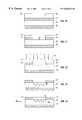
- FIG. 1illustrates a side cross-sectional view of a portion of a wafer having a first metal layer 10 and a second metal layer 12 separated by an ILD layer 14 .
- a continuous need in the manufacturing of semiconductor wafersis the reduction of the interconnect capacitance of a wafer.
- Cis the capacitance of a structure
- ⁇is the dielectric constant of a material within the structure
- Ais the cross-sectional area of the structure
- dis the distance between the two electrodes.
- the ILD layeris comprised of silicon oxide (SiO 2 ), which has a dielectric constant of 4.
- the lowest dielectric constant possibleis 1, which is the dielectric constant associated with an air gap (or vacuum).
- a method of decreasing the dielectric constant of a dielectric layeris described. First, a dielectric layer is formed on a first conductive layer. A substance is then implanted into the dielectric layer.
- FIG. 1is a side cross-sectional view of a portion of a wafer having two metal layers separated by an inter-level dielectric (ILD) layer.
- ILDinter-level dielectric
- FIG. 2is a side cross-sectional view of a substrate having gaseous implants therein.
- FIG. 3is a side cross-sectional view of a dielectric layer during implantation of a gaseous substance.
- FIG. 4is a side cross-sectional view of the voids formed in the dielectric layer after annealing.
- FIG. 5is a side cross-sectional view of the device of FIG. 4 with a second metal layer deposited above the dielectric layer.
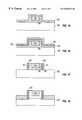
- FIG. 6is a side cross-sectional view of a dielectric layer having a photoresist mask positioned thereon.
- FIG. 7is a side cross-sectional view of the dielectric layer of FIG. 6 after etching to create a cavity.
- FIG. 8is a side cross-sectional view of the device of FIG. 7 during implantation of a gaseous substance.
- FIG. 9is a side cross-sectional view of the device of FIG. 9 illustrating the formation of the voids in the dielectric layer after annealing and the deposition of a second conductive layer in the previously formed cavity.
- FIG. 10is a side cross-sectional view of a device comprising a first and second conductive layer separated by a dielectric layer having a photoresist mask atop the second conductive layer.
- FIG. 11is a side cross-sectional view of the device of FIG. 10 after etching of the second conductive layer to form a trench.
- FIG. 12is a side cross-sectional view of the device of FIG. 11 during implantation of a gaseous substance.
- FIG. 13is a side cross-sectional view of the device of FIG. 12 after the formation of the voids in the dielectric layer and the removal of the mask.
- FIG. 14is a side cross-sectional view of the device of FIG. 13 with a second dielectric layer deposited in the previously formed trench.
- FIG. 15is a side cross-sectional view of a gate structure having a layer of nitride deposited thereon.
- FIG. 16is a side cross-sectional view of the device of FIG. 15 after implantation of a gaseous substance.
- FIG. 17is a side cross-sectional view of the device of FIG. 16 after etching of the nitride layer.
- FIG. 18is a side cross-sectional view of the device of FIG. 17 after formation of the source and drain junctions through selective epitaxy.
- ILDinter-level dielectric
- the present inventionrelates to a method of forming voids (also referred to as cavities, holes, bubbles, etc.) in an ILD to decrease the dielectric constant ( ⁇ ) associated with the given ILD. Because the dielectric constant ( ⁇ ) associated with the voids is significantly lower than that associated with the original material of the ILD, the overall dielectric constant ( ⁇ ) of the ILD having the implanted voids will be less than that of the original ILD without the voids. Because the capacitance of a device is directly proportional to the dielectric constant ( ⁇ ) of the material of the device, the capacitance for a device fabricated from the wafer containing the modified ILD and having the decreased dielectric constant ( ⁇ ) will also decrease.
- voidsalso referred to as cavities, holes, bubbles, etc.
- the substance to be implanted into the ILDmay be any one of or combination of several different gases, including but not limited to the noble gases and oxygen. Other possible species which react to form voids or gaseous regions may also be used.
- argonis the gaseous substance implanted into the substrate of the to-be-formed device. For illustrative purposes only, the following embodiments of the present invention will be discussed with use of argon-formed voids.
- FIG. 3is a side cross-sectional view of a first conductive layer (e.g., metal layer) 20 having an ILD layer 22 formed thereon.
- a gaseous implantation 24is applied at an energy of approximately 135 keV (kilo electron volts) and a dosage of approximately 10 16 to 10 17 atoms/cm 2 .
- the depth of the implantation into the ILD layer (e.g., SiO 2 ) 22is approximately 1500 ⁇ . Note that the depth of the implantation is controlled by the energy of the implant and may be modified as required by the size of a given device.
- the damageis caused by the gaseous substance 24 to the ILD 22 .
- the damagemay be comprised of displaced atoms, broken bonds, etc.
- the damage to the ILD 22 of FIG. 3begins to anneal away and the formation of voids 26 in the resulting ILD 22 A begins, as illustrated in FIG. 4 .
- a second conductive layer 28is added above the ILD 22 A and a capacitor 30 may be etched and formed having a reduced dielectric constant ( ⁇ ) (see FIG. 5 ).
- the dielectric constant ( ⁇ ) of the ILD 22 Ais a function of the dielectric constant ( ⁇ ) of the original ILD material 22 and the dielectric constant ( ⁇ ) of the voids 26 .
- the dielectric constant ( ⁇ ) of the ILD 22 A having voids 26is reduced by approximately 12% when compared to that of the original ILD 22 .
- a second embodiment of the present inventionaddresses intra-line capacitance.
- This embodimentutilizes the damascene process of fabrication and is illustrated in FIGS. 6-9.
- a photoresist mask 44is applied to the ILD layer 42 residing above a first conductive layer 40 (see FIG. 6 ).
- the ILD layer 42is then etched such that a cavity 46 is formed in the region of the ILD layer 42 left exposed by the mask 44 (see FIG. 7 ).
- gaseous substances 48are implanted into the ILD layer 42 , including the cavity 46 (see FIG. 8 ). As illustrated in FIG.
- the implantationresults in an ILD layer 42 having voids 50 formed along the surface of the ILD layer 42 , with the conductive line 52 formed within the previously etched cavity 46 .
- the gaseous implantmay be performed after the etch to open the ILD up for subsequent metal deposition.
- FIGS. 10-14A third embodiment is illustrated in FIGS. 10-14.
- FIG. 10is a side cross-sectional view illustrating a first conductive layer 70 , a dielectric layer 72 , a second conductive layer 74 , and a photoresist mask 76 applied thereto.
- FIG. 11illustrates the device of FIG. 10 after the second conductive layer 74 has been etched to form a trench 78 .
- a gaseous substance 77is then implanted into the device prior to the removal of the photoresist mask 76 (see FIG. 12 ).
- the photoresist mask 76is removed.
- a subsequent dielectric layer 73is then formed in the trench 78 to form the final device 82 illustrated in FIG. 14 .
- the above-described third embodimentfills the less critical diagonal lines and fringing capacitances.
- a blanket implant following the ILD depositioneither as inter-level dielectric, or intra-level dielectric, could also serve the same purpose.
- any voids in the interconnect systemhave the potential for weakening the interconnect ILD integrity to mechanical stress. Since the top surface of the interconnect is uncovered in this last process, however, this might allow for some relaxation of the potential stress that could result from the process.
- the present inventionmay also be applied to an MOS transistor for reduction of the overlap capacitance.
- an MOS transistorfor reduction of the overlap capacitance.
- FIGS. 15-18An embodiment illustrating use of the present invention with an MOS transistor is depicted in FIGS. 15-18.
- FIG. 15is a side cross-sectional view of a gate structure comprising a silicon layer 90 with a polysilicon layer 94 deposited thereon and separated by an oxide layer 96 .
- the gate structurethen has a layer of nitride 92 deposited thereon.
- the nitride layeris approximately 600-1200 ⁇ and the oxide layer 96 is approximately 100 ⁇ .
- FIG. 16illustrates the device of FIG. 15 after the implantation of a gaseous substance such as Helium. The implantation of Helium results in the presence of a helium layer 98 caused by the implant within the nitride layer 92 .
- Etching the nitride layer 92see FIG. 17
- forming the source and drain junctions through selective epitaxysee FIG. 18 then completes the process.
- the overlap capacitance of the transistoris reduced by approximately 25%.
- the dielectric constant of the dielectric layeris reduced, which in turn reduces the capacitance associated with the dielectric layer.
- the global dielectric constant of an inter-metal dielectricmay be decreased and consequently the speed of integrated circuits may be increased.
Landscapes
- Engineering & Computer Science (AREA)
- Physics & Mathematics (AREA)
- Condensed Matter Physics & Semiconductors (AREA)
- General Physics & Mathematics (AREA)
- Computer Hardware Design (AREA)
- Microelectronics & Electronic Packaging (AREA)
- Power Engineering (AREA)
- Manufacturing & Machinery (AREA)
- Plasma & Fusion (AREA)
- Internal Circuitry In Semiconductor Integrated Circuit Devices (AREA)
- Insulated Gate Type Field-Effect Transistor (AREA)
Abstract
Description
Applications related to the present invention include: (1) application Ser. No. 09/340,583, filed Jun. 28,1999, entitled Method of Increasing the Mobility of MOS Transistors by Use of Localized Stress Regions, which issued as U.S. Pat. No. 6,228,694 on May 8, 2001; (2) application Ser. No. 09/340,954, filed Jun. 28, 1999, entitled Technique to Obtain Increased Channel Mobilities in NMOS Transistors by Gate Electrode Enqineering, which issued as U.S. Pat. No. 6,281,532 on Aug. 28, 2001; (3) application Ser. No. 09/342,030, filed Jun. 28, 1999, entitled Methodology for Control of Short Channel Effects in MOS Transistors, which issued as U.S. Pat. No. 6,362,082 on Mar. 26, 2002; (4) application Ser. No. 10/045,346, filed Nov. 9, 2001, entitled Methodology for Control of Short Channel Effects in MOS Transistors, which is a divisional of application Ser. No. 09/342,030. Each of the related applications listed above has been assigned to the assignee of the present invention.
1. Field of the Invention
A method of decreasing the global dielectric constant of an inter-level dielectric is described. More particularly, the present invention relates to the use of implants into the inter-level dielectric to decrease the global dielectric constant.
2. Description of Related Art
Semiconductor wafers are fabricated using a substrate having stacked layers, generally a first metal layer, then an inter-level dielectric (ILD) layer, then a second metal layer, etc. FIG. 1 illustrates a side cross-sectional view of a portion of a wafer having afirst metal layer 10 and asecond metal layer 12 separated by anILD layer 14.
A continuous need in the manufacturing of semiconductor wafers is the reduction of the interconnect capacitance of a wafer. The capacitance of a structure may be calculated using the formula

wherein C is the capacitance of a structure, ∈ is the dielectric constant of a material within the structure, A is the cross-sectional area of the structure, and d is the distance between the two electrodes. Thus, to achieve the goal of lowering the capacitance of a material as much as possible, the dielectric constant (∈) must also be lowered as much as possible.
Typically, the ILD layer is comprised of silicon oxide (SiO2), which has a dielectric constant of 4. The lowest dielectric constant possible is 1, which is the dielectric constant associated with an air gap (or vacuum). By merely modifying the currently used ILD layer of silicon oxide, there is consequently little need to address the integration issues, such as etchability, adhesion, etc., that arise when a new and different ILD layer, such as one fabricated from a polymer material, is used. Thus, it would be desirable to modify the ILD layer such that silicon oxide could still be used as the primary material, but the modified ILD layer would have a smaller dielectric constant than the dielectric constant of 4 associated with silicon oxide.
A method of decreasing the dielectric constant of a dielectric layer is described. First, a dielectric layer is formed on a first conductive layer. A substance is then implanted into the dielectric layer.
The invention is further described by way of example with reference to the accompanying drawings, wherein:
FIG. 1 is a side cross-sectional view of a portion of a wafer having two metal layers separated by an inter-level dielectric (ILD) layer.
FIG. 2 is a side cross-sectional view of a substrate having gaseous implants therein.
FIG. 3 is a side cross-sectional view of a dielectric layer during implantation of a gaseous substance.
FIG. 4 is a side cross-sectional view of the voids formed in the dielectric layer after annealing.
FIG. 5 is a side cross-sectional view of the device of FIG. 4 with a second metal layer deposited above the dielectric layer.
FIG. 6 is a side cross-sectional view of a dielectric layer having a photoresist mask positioned thereon.
FIG. 7 is a side cross-sectional view of the dielectric layer of FIG. 6 after etching to create a cavity.
FIG. 8 is a side cross-sectional view of the device of FIG. 7 during implantation of a gaseous substance.
FIG. 9 is a side cross-sectional view of the device of FIG. 9 illustrating the formation of the voids in the dielectric layer after annealing and the deposition of a second conductive layer in the previously formed cavity.
FIG. 10 is a side cross-sectional view of a device comprising a first and second conductive layer separated by a dielectric layer having a photoresist mask atop the second conductive layer.
FIG. 11 is a side cross-sectional view of the device of FIG. 10 after etching of the second conductive layer to form a trench.
FIG. 12 is a side cross-sectional view of the device of FIG. 11 during implantation of a gaseous substance.
FIG. 13 is a side cross-sectional view of the device of FIG. 12 after the formation of the voids in the dielectric layer and the removal of the mask.
FIG. 14 is a side cross-sectional view of the device of FIG. 13 with a second dielectric layer deposited in the previously formed trench.
FIG. 15 is a side cross-sectional view of a gate structure having a layer of nitride deposited thereon.
FIG. 16 is a side cross-sectional view of the device of FIG. 15 after implantation of a gaseous substance.
FIG. 17 is a side cross-sectional view of the device of FIG. 16 after etching of the nitride layer.
FIG. 18 is a side cross-sectional view of the device of FIG. 17 after formation of the source and drain junctions through selective epitaxy.
A method of using implants in an inter-level dielectric (ILD) layer is described. The implants lower the dielectric constant of the ILD and thus lower the capacitance associated with devices formed therefrom. In the following description, numerous specific details are set forth such as specific materials, process parameters, dimensions, etc. in order to provide a thorough understanding of the present invention. It will be obvious, however, to one skilled in the art that these specific details need not be employed to practice the present invention. In other instances, well-known materials or methods have not been described in detail in order to avoid unnecessarily obscuring the present invention.
The present invention relates to a method of forming voids (also referred to as cavities, holes, bubbles, etc.) in an ILD to decrease the dielectric constant (∈) associated with the given ILD. Because the dielectric constant (∈) associated with the voids is significantly lower than that associated with the original material of the ILD, the overall dielectric constant (∈) of the ILD having the implanted voids will be less than that of the original ILD without the voids. Because the capacitance of a device is directly proportional to the dielectric constant (∈) of the material of the device, the capacitance for a device fabricated from the wafer containing the modified ILD and having the decreased dielectric constant (∈) will also decrease.
The substance to be implanted into the ILD may be any one of or combination of several different gases, including but not limited to the noble gases and oxygen. Other possible species which react to form voids or gaseous regions may also be used. In one embodiment of the present invention, argon is the gaseous substance implanted into the substrate of the to-be-formed device. For illustrative purposes only, the following embodiments of the present invention will be discussed with use of argon-formed voids.
The implantation of voids into a substrate is known and will not be discussed in detail herein. Thus, a conventional implanter may be used to implant the gaseous substance into the ILD. One embodiment of the present invention is illustrated in FIGS. 3 and 4. FIG. 3 is a side cross-sectional view of a first conductive layer (e.g., metal layer)20 having anILD layer 22 formed thereon. Agaseous implantation 24 is applied at an energy of approximately 135 keV (kilo electron volts) and a dosage of approximately 1016to 1017atoms/cm2. In this embodiment, the depth of the implantation into the ILD layer (e.g., SiO2)22 is approximately 1500 Å. Note that the depth of the implantation is controlled by the energy of the implant and may be modified as required by the size of a given device.
As thegaseous substance 24 is introduced into theILD 22, damage is caused by thegaseous substance 24 to theILD 22. The damage may be comprised of displaced atoms, broken bonds, etc. As theILD 22 is annealed at approximately 400-500° C. for approximately 30 seconds, the damage to theILD 22 of FIG. 3 begins to anneal away and the formation ofvoids 26 in the resultingILD 22A begins, as illustrated in FIG.4.
After thevoids 26 have been formed in theILD 22A, a secondconductive layer 28 is added above theILD 22A and acapacitor 30 may be etched and formed having a reduced dielectric constant (∈) (see FIG.5). The dielectric constant (∈) of theILD 22A is a function of the dielectric constant (∈) of theoriginal ILD material 22 and the dielectric constant (∈) of thevoids 26. In the above described embodiment, the dielectric constant (∈) of theILD 22 A having voids 26 is reduced by approximately 12% when compared to that of theoriginal ILD 22.
A second embodiment of the present invention addresses intra-line capacitance. This embodiment utilizes the damascene process of fabrication and is illustrated in FIGS. 6-9. First, aphotoresist mask 44 is applied to theILD layer 42 residing above a first conductive layer40 (see FIG.6). TheILD layer 42 is then etched such that acavity 46 is formed in the region of theILD layer 42 left exposed by the mask44 (see FIG.7). After themask 44 is removed,gaseous substances 48 are implanted into theILD layer 42, including the cavity46 (see FIG.8). As illustrated in FIG. 9, the implantation results in anILD layer 42 havingvoids 50 formed along the surface of theILD layer 42, with theconductive line 52 formed within the previously etchedcavity 46. In this manner, the gaseous implant may be performed after the etch to open the ILD up for subsequent metal deposition. Thus, the above described process requires no additional lithography steps over the current method of fabrication, but still results in voids formed in the dielectric layer which give the inter-level conductive system its reduced dielectric constant (∈).
A third embodiment is illustrated in FIGS. 10-14. In this third embodiment, a similar process is followed for a subtractive metal approach. FIG. 10 is a side cross-sectional view illustrating a firstconductive layer 70, adielectric layer 72, a secondconductive layer 74, and aphotoresist mask 76 applied thereto. FIG. 11 illustrates the device of FIG. 10 after the secondconductive layer 74 has been etched to form atrench 78. Agaseous substance 77 is then implanted into the device prior to the removal of the photoresist mask76 (see FIG.12). Next, as illustrated in FIG. 13, thephotoresist mask 76 is removed. Asubsequent dielectric layer 73 is then formed in thetrench 78 to form thefinal device 82 illustrated in FIG.14.
The above-described third embodiment fills the less critical diagonal lines and fringing capacitances. A blanket implant following the ILD deposition, either as inter-level dielectric, or intra-level dielectric, could also serve the same purpose. However, there are potential reliability problems with this alternative approach. For example, any voids in the interconnect system have the potential for weakening the interconnect ILD integrity to mechanical stress. Since the top surface of the interconnect is uncovered in this last process, however, this might allow for some relaxation of the potential stress that could result from the process.
The present invention may also be applied to an MOS transistor for reduction of the overlap capacitance. With structures having elevated source/drain structures, it is expected that the overlap capacitance will become a more substantial fraction of the transistor's capacitance than the conventional planar transistor. Consequently, the concept of a spacer having a low dielectric constant (∈) is of importance. An embodiment illustrating use of the present invention with an MOS transistor is depicted in FIGS. 15-18.
FIG. 15 is a side cross-sectional view of a gate structure comprising asilicon layer 90 with apolysilicon layer 94 deposited thereon and separated by anoxide layer 96. The gate structure then has a layer ofnitride 92 deposited thereon. In one embodiment, the nitride layer is approximately 600-1200 Å and theoxide layer 96 is approximately 100 Å. FIG. 16 illustrates the device of FIG. 15 after the implantation of a gaseous substance such as Helium. The implantation of Helium results in the presence of ahelium layer 98 caused by the implant within thenitride layer 92. Etching the nitride layer92 (see FIG. 17) and forming the source and drain junctions through selective epitaxy (see FIG. 18) then completes the process. When comparing the device of FIG. 18 with an unimplanted device, the overlap capacitance of the transistor is reduced by approximately 25%.
Thus, by implanting voids in the dielectric layer, the dielectric constant of the dielectric layer is reduced, which in turn reduces the capacitance associated with the dielectric layer. In this manner, the global dielectric constant of an inter-metal dielectric may be decreased and consequently the speed of integrated circuits may be increased.
Claims (21)
1. A method comprising:
forming a dielectric layer on a first conductive layer; and
implanting a substance into said dielectric layer without implanting said substance into said first conductive layer in order to decrease a dielectric constant of the dielectric layer;
wherein said implanting the substance further comprises implanting a gaseous substance into said dielectric layer, wherein said gaseous substance is selected from a group consisting of the noble gases, oxygen, and any combination thereof.
2. A method comprising:
forming a dielectric layer on a first conductive layer; and
implanting a substance into said dielectric layer without implanting said substance into said first conductive layer in order to decrease a dielectric constant of the dielectric layer;
wherein implanting a substance further comprises implanting a substance at a dosage of approximately 1016to 1017atoms/cm2.
3. A method comprising:
forming a dielectric layer on a first conductive layer;
implanting a substance into said dielectric layer without implanting said substance into said first conductive layer in order to decrease a dielectric constant of the dielectric layer; and
annealing said dielectric layer at approximately 400° C. such that said implanted substance forms at least one void in said dielectric layer.
4. The method ofclaim 3 wherein annealing said dielectric layer further comprises annealing said dielectric layer for at least 30 seconds such that said implanted substance forms at least one void in said dielectric layer.
5. A method comprising:
forming a dielectric layer on a first conductive layer;
implanting a substance into said dielectric layer without implanting said substance into said first conductive layer in order to decrease a dielectric constant of the dielectric layer; and
forming a second conductive layer adjacent said dielectric layer.
6. A method of decreasing the dielectric constant of a dielectric layer comprising:
forming a dielectric layer on a first conductive layer;
etching said dielectric layer to form a cavity;
implanting a substance into said dielectric layer; and,
depositing a second conductive layer in said cavity.
7. The method ofclaim 6 wherein said implanting a substance further comprises implanting a gaseous substance into said dielectric layer, wherein said substance is selected from a group consisting of the noble gases, oxygen, and any combination thereof.
8. The method ofclaim 7 wherein said implanting a substance further comprises implanting a substance at an energy level of approximately 135 keV.
9. The method ofclaim 8 wherein said implanting a substance further comprises implanting a substance at a dosage of approximately 1016to 1017atoms/cm2.
10. The method ofclaim 6 further comprising annealing said dielectric layer such that said implanted substance forms at least one void in said dielectric layer.
11. The method ofclaim 10 wherein said annealing said dielectric layer further comprises annealing said dielectric layer at approximately 400° C. such that said implanted substance forms at least one void in said dielectric layer.
12. A method of decreasing the dielectric constant of a dielectric layer, comprising:
forming a first dielectric layer on a first conductive layer;
forming a second conductive layer on said first dielectric layer;
etching said second conductive layer to form a trench, such that a portion of said first dielectric layer is exposed;
implanting a substance into said exposed portion of said first dielectric layer; and,
depositing a second dielectric layer in said trench.
13. The method ofclaim 12 wherein said implanting a substance further comprises implanting a gaseous substance into said first dielectric layer, wherein said substance is selected from a group consisting of the noble gases, oxygen, and any combination thereof.
14. The method ofclaim 12 wherein said implanting a substance further comprises implanting a substance at an energy level of approximately 135 keV.
15. The method ofclaim 14 wherein said implanting a substance further comprises implanting a substance at a dosage of approximately 1016to 1017atoms/cm2.
16. The method ofclaim 12 further comprising annealing said first dielectric layer such that said implanted substance forms at least one void in said dielectric layer.
17. The method ofclaim 16 wherein said annealing said first dielectric layer further comprises annealing said first dielectric layer at approximately 400° C. such that said implanted substance forms at least one void in said first dielectric layer.
18. A method of decreasing the overlap capacitance of a transistor, comprising:
forming a gate electrode;
forming a nitride layer on said gate electrode;
implanting a substance into said nitride layer;
etching said nitride layer; and,
forming a source and drain junction through selective epitaxy.
19. The method ofclaim 18 wherein said implanting a substance further comprises implanting a gaseous substance into said first dielectric layer, wherein said gaseous substance is selected from the group consisting of the noble gases, oxygen, and any combination thereof.
20. The method ofclaim 18 wherein said implanting a substance further comprises implanting a substance at an energy level of approximately 135 keV.
21. The method ofclaim 20 wherein said implanting a substance further comprises implanting a substance at a dosage of approximately 1016to 1017atoms/cm2.
Priority Applications (1)
| Application Number | Priority Date | Filing Date | Title |
|---|---|---|---|
| US09/344,918US6656822B2 (en) | 1999-06-28 | 1999-06-28 | Method for reduced capacitance interconnect system using gaseous implants into the ILD |
Applications Claiming Priority (1)
| Application Number | Priority Date | Filing Date | Title |
|---|---|---|---|
| US09/344,918US6656822B2 (en) | 1999-06-28 | 1999-06-28 | Method for reduced capacitance interconnect system using gaseous implants into the ILD |
Publications (2)
| Publication Number | Publication Date |
|---|---|
| US20020090791A1 US20020090791A1 (en) | 2002-07-11 |
| US6656822B2true US6656822B2 (en) | 2003-12-02 |
Family
ID=23352667
Family Applications (1)
| Application Number | Title | Priority Date | Filing Date |
|---|---|---|---|
| US09/344,918Expired - Fee RelatedUS6656822B2 (en) | 1999-06-28 | 1999-06-28 | Method for reduced capacitance interconnect system using gaseous implants into the ILD |
Country Status (1)
| Country | Link |
|---|---|
| US (1) | US6656822B2 (en) |
Cited By (19)
| Publication number | Priority date | Publication date | Assignee | Title |
|---|---|---|---|---|
| US20040173798A1 (en)* | 2003-03-05 | 2004-09-09 | Micron Technology, Inc. | Micro-mechanically strained semiconductor film |
| US20040217896A1 (en)* | 2003-01-24 | 2004-11-04 | Stmicroelectronics S.R.L | Multistage analog-to-digital converter |
| US20040217391A1 (en)* | 2003-04-29 | 2004-11-04 | Micron Technology, Inc. | Localized strained semiconductor on insulator |
| US20050017273A1 (en)* | 2003-07-21 | 2005-01-27 | Micron Technology, Inc. | Gettering using voids formed by surface transformation |
| US20050026388A1 (en)* | 2002-07-18 | 2005-02-03 | Micron Technology, Inc. | Techniques to create low K ILD for BEOL |
| US7008854B2 (en) | 2003-05-21 | 2006-03-07 | Micron Technology, Inc. | Silicon oxycarbide substrates for bonded silicon on insulator |
| US7142577B2 (en) | 2001-05-16 | 2006-11-28 | Micron Technology, Inc. | Method of forming mirrors by surface transformation of empty spaces in solid state materials and structures thereon |
| US7153753B2 (en) | 2003-08-05 | 2006-12-26 | Micron Technology, Inc. | Strained Si/SiGe/SOI islands and processes of making same |
| US7164188B2 (en) | 2000-12-13 | 2007-01-16 | Micron Technology, Inc. | Buried conductor patterns formed by surface transformation of empty spaces in solid state materials |
| US7166524B2 (en)* | 2000-08-11 | 2007-01-23 | Applied Materials, Inc. | Method for ion implanting insulator material to reduce dielectric constant |
| US7271445B2 (en) | 2003-05-21 | 2007-09-18 | Micron Technology, Inc. | Ultra-thin semiconductors bonded on glass substrates |
| US7393765B2 (en) | 2002-06-05 | 2008-07-01 | Applied Materials, Inc. | Low temperature CVD process with selected stress of the CVD layer on CMOS devices |
| US20090026879A1 (en)* | 2005-10-25 | 2009-01-29 | Prelas Mark A | Micro-Scale Power Source |
| US7501329B2 (en) | 2003-05-21 | 2009-03-10 | Micron Technology, Inc. | Wafer gettering using relaxed silicon germanium epitaxial proximity layers |
| US20090140341A1 (en)* | 2007-11-30 | 2009-06-04 | Ravi Pillarisetty | Independent n-tips for multi-gate transistors |
| US7662701B2 (en) | 2003-05-21 | 2010-02-16 | Micron Technology, Inc. | Gettering of silicon on insulator using relaxed silicon germanium epitaxial proximity layers |
| US7964124B2 (en) | 2002-01-17 | 2011-06-21 | Micron Technology, Inc. | Method of forming cellular material |
| US8227309B2 (en) | 2006-02-16 | 2012-07-24 | Micron Technology, Inc. | Localized compressive strained semiconductor |
| US20160359044A1 (en)* | 2015-06-04 | 2016-12-08 | International Business Machines Corporation | FORMATION OF DISLOCATION-FREE SiGe FINFET USING POROUS SILICON |
Families Citing this family (73)
| Publication number | Priority date | Publication date | Assignee | Title |
|---|---|---|---|---|
| US7388259B2 (en)* | 2002-11-25 | 2008-06-17 | International Business Machines Corporation | Strained finFET CMOS device structures |
| US6887798B2 (en) | 2003-05-30 | 2005-05-03 | International Business Machines Corporation | STI stress modification by nitrogen plasma treatment for improving performance in small width devices |
| US7329923B2 (en)* | 2003-06-17 | 2008-02-12 | International Business Machines Corporation | High-performance CMOS devices on hybrid crystal oriented substrates |
| US7279746B2 (en) | 2003-06-30 | 2007-10-09 | International Business Machines Corporation | High performance CMOS device structures and method of manufacture |
| US7410846B2 (en) | 2003-09-09 | 2008-08-12 | International Business Machines Corporation | Method for reduced N+ diffusion in strained Si on SiGe substrate |
| US6890808B2 (en)* | 2003-09-10 | 2005-05-10 | International Business Machines Corporation | Method and structure for improved MOSFETs using poly/silicide gate height control |
| US6887751B2 (en)* | 2003-09-12 | 2005-05-03 | International Business Machines Corporation | MOSFET performance improvement using deformation in SOI structure |
| US7170126B2 (en) | 2003-09-16 | 2007-01-30 | International Business Machines Corporation | Structure of vertical strained silicon devices |
| US6869866B1 (en) | 2003-09-22 | 2005-03-22 | International Business Machines Corporation | Silicide proximity structures for CMOS device performance improvements |
| US6872641B1 (en)* | 2003-09-23 | 2005-03-29 | International Business Machines Corporation | Strained silicon on relaxed sige film with uniform misfit dislocation density |
| US7144767B2 (en)* | 2003-09-23 | 2006-12-05 | International Business Machines Corporation | NFETs using gate induced stress modulation |
| US7119403B2 (en)* | 2003-10-16 | 2006-10-10 | International Business Machines Corporation | High performance strained CMOS devices |
| US7037770B2 (en)* | 2003-10-20 | 2006-05-02 | International Business Machines Corporation | Method of manufacturing strained dislocation-free channels for CMOS |
| US7303949B2 (en) | 2003-10-20 | 2007-12-04 | International Business Machines Corporation | High performance stress-enhanced MOSFETs using Si:C and SiGe epitaxial source/drain and method of manufacture |
| US7129126B2 (en)* | 2003-11-05 | 2006-10-31 | International Business Machines Corporation | Method and structure for forming strained Si for CMOS devices |
| US7015082B2 (en)* | 2003-11-06 | 2006-03-21 | International Business Machines Corporation | High mobility CMOS circuits |
| US7029964B2 (en)* | 2003-11-13 | 2006-04-18 | International Business Machines Corporation | Method of manufacturing a strained silicon on a SiGe on SOI substrate |
| US7122849B2 (en)* | 2003-11-14 | 2006-10-17 | International Business Machines Corporation | Stressed semiconductor device structures having granular semiconductor material |
| US7247534B2 (en) | 2003-11-19 | 2007-07-24 | International Business Machines Corporation | Silicon device on Si:C-OI and SGOI and method of manufacture |
| US7198995B2 (en)* | 2003-12-12 | 2007-04-03 | International Business Machines Corporation | Strained finFETs and method of manufacture |
| US7247912B2 (en)* | 2004-01-05 | 2007-07-24 | International Business Machines Corporation | Structures and methods for making strained MOSFETs |
| US7118999B2 (en) | 2004-01-16 | 2006-10-10 | International Business Machines Corporation | Method and apparatus to increase strain effect in a transistor channel |
| US7202132B2 (en) | 2004-01-16 | 2007-04-10 | International Business Machines Corporation | Protecting silicon germanium sidewall with silicon for strained silicon/silicon germanium MOSFETs |
| US7381609B2 (en) | 2004-01-16 | 2008-06-03 | International Business Machines Corporation | Method and structure for controlling stress in a transistor channel |
| US7923782B2 (en)* | 2004-02-27 | 2011-04-12 | International Business Machines Corporation | Hybrid SOI/bulk semiconductor transistors |
| US7205206B2 (en)* | 2004-03-03 | 2007-04-17 | International Business Machines Corporation | Method of fabricating mobility enhanced CMOS devices |
| US7504693B2 (en)* | 2004-04-23 | 2009-03-17 | International Business Machines Corporation | Dislocation free stressed channels in bulk silicon and SOI CMOS devices by gate stress engineering |
| US7223994B2 (en)* | 2004-06-03 | 2007-05-29 | International Business Machines Corporation | Strained Si on multiple materials for bulk or SOI substrates |
| US7037794B2 (en) | 2004-06-09 | 2006-05-02 | International Business Machines Corporation | Raised STI process for multiple gate ox and sidewall protection on strained Si/SGOI structure with elevated source/drain |
| TWI463526B (en) | 2004-06-24 | 2014-12-01 | Ibm | Method for improving stress-induced CMOS components and components prepared by the method |
| US7227205B2 (en) | 2004-06-24 | 2007-06-05 | International Business Machines Corporation | Strained-silicon CMOS device and method |
| US7288443B2 (en)* | 2004-06-29 | 2007-10-30 | International Business Machines Corporation | Structures and methods for manufacturing p-type MOSFET with graded embedded silicon-germanium source-drain and/or extension |
| US7217949B2 (en)* | 2004-07-01 | 2007-05-15 | International Business Machines Corporation | Strained Si MOSFET on tensile-strained SiGe-on-insulator (SGOI) |
| US6991998B2 (en)* | 2004-07-02 | 2006-01-31 | International Business Machines Corporation | Ultra-thin, high quality strained silicon-on-insulator formed by elastic strain transfer |
| US7384829B2 (en) | 2004-07-23 | 2008-06-10 | International Business Machines Corporation | Patterned strained semiconductor substrate and device |
| US7193254B2 (en)* | 2004-11-30 | 2007-03-20 | International Business Machines Corporation | Structure and method of applying stresses to PFET and NFET transistor channels for improved performance |
| US7238565B2 (en) | 2004-12-08 | 2007-07-03 | International Business Machines Corporation | Methodology for recovery of hot carrier induced degradation in bipolar devices |
| US7262087B2 (en)* | 2004-12-14 | 2007-08-28 | International Business Machines Corporation | Dual stressed SOI substrates |
| US7173312B2 (en)* | 2004-12-15 | 2007-02-06 | International Business Machines Corporation | Structure and method to generate local mechanical gate stress for MOSFET channel mobility modification |
| US7274084B2 (en)* | 2005-01-12 | 2007-09-25 | International Business Machines Corporation | Enhanced PFET using shear stress |
| US20060160317A1 (en)* | 2005-01-18 | 2006-07-20 | International Business Machines Corporation | Structure and method to enhance stress in a channel of cmos devices using a thin gate |
| US7432553B2 (en)* | 2005-01-19 | 2008-10-07 | International Business Machines Corporation | Structure and method to optimize strain in CMOSFETs |
| US7220626B2 (en)* | 2005-01-28 | 2007-05-22 | International Business Machines Corporation | Structure and method for manufacturing planar strained Si/SiGe substrate with multiple orientations and different stress levels |
| FR2881419B1 (en)* | 2005-01-28 | 2007-11-09 | Centre Nat Rech Scient | PROCESS FOR PRODUCING A MATERIAL BASED ON SILICON OXIDE AND WITH LOW DIELECTRIC CONSTANT |
| US7256081B2 (en)* | 2005-02-01 | 2007-08-14 | International Business Machines Corporation | Structure and method to induce strain in a semiconductor device channel with stressed film under the gate |
| US7224033B2 (en) | 2005-02-15 | 2007-05-29 | International Business Machines Corporation | Structure and method for manufacturing strained FINFET |
| US7545004B2 (en)* | 2005-04-12 | 2009-06-09 | International Business Machines Corporation | Method and structure for forming strained devices |
| US7544577B2 (en)* | 2005-08-26 | 2009-06-09 | International Business Machines Corporation | Mobility enhancement in SiGe heterojunction bipolar transistors |
| US7202513B1 (en)* | 2005-09-29 | 2007-04-10 | International Business Machines Corporation | Stress engineering using dual pad nitride with selective SOI device architecture |
| US20070096170A1 (en)* | 2005-11-02 | 2007-05-03 | International Business Machines Corporation | Low modulus spacers for channel stress enhancement |
| US7655511B2 (en) | 2005-11-03 | 2010-02-02 | International Business Machines Corporation | Gate electrode stress control for finFET performance enhancement |
| US7785950B2 (en)* | 2005-11-10 | 2010-08-31 | International Business Machines Corporation | Dual stress memory technique method and related structure |
| US7348638B2 (en)* | 2005-11-14 | 2008-03-25 | International Business Machines Corporation | Rotational shear stress for charge carrier mobility modification |
| US7709317B2 (en) | 2005-11-14 | 2010-05-04 | International Business Machines Corporation | Method to increase strain enhancement with spacerless FET and dual liner process |
| US7564081B2 (en) | 2005-11-30 | 2009-07-21 | International Business Machines Corporation | finFET structure with multiply stressed gate electrode |
| US7776695B2 (en)* | 2006-01-09 | 2010-08-17 | International Business Machines Corporation | Semiconductor device structure having low and high performance devices of same conductive type on same substrate |
| US7863197B2 (en) | 2006-01-09 | 2011-01-04 | International Business Machines Corporation | Method of forming a cross-section hourglass shaped channel region for charge carrier mobility modification |
| US7635620B2 (en) | 2006-01-10 | 2009-12-22 | International Business Machines Corporation | Semiconductor device structure having enhanced performance FET device |
| US20070158743A1 (en)* | 2006-01-11 | 2007-07-12 | International Business Machines Corporation | Thin silicon single diffusion field effect transistor for enhanced drive performance with stress film liners |
| US7691698B2 (en) | 2006-02-21 | 2010-04-06 | International Business Machines Corporation | Pseudomorphic Si/SiGe/Si body device with embedded SiGe source/drain |
| US8461009B2 (en)* | 2006-02-28 | 2013-06-11 | International Business Machines Corporation | Spacer and process to enhance the strain in the channel with stress liner |
| US7615418B2 (en) | 2006-04-28 | 2009-11-10 | International Business Machines Corporation | High performance stress-enhance MOSFET and method of manufacture |
| US7521307B2 (en)* | 2006-04-28 | 2009-04-21 | International Business Machines Corporation | CMOS structures and methods using self-aligned dual stressed layers |
| US7608489B2 (en)* | 2006-04-28 | 2009-10-27 | International Business Machines Corporation | High performance stress-enhance MOSFET and method of manufacture |
| US8853746B2 (en) | 2006-06-29 | 2014-10-07 | International Business Machines Corporation | CMOS devices with stressed channel regions, and methods for fabricating the same |
| US7790540B2 (en) | 2006-08-25 | 2010-09-07 | International Business Machines Corporation | Structure and method to use low k stress liner to reduce parasitic capacitance |
| US7462522B2 (en)* | 2006-08-30 | 2008-12-09 | International Business Machines Corporation | Method and structure for improving device performance variation in dual stress liner technology |
| US8754446B2 (en) | 2006-08-30 | 2014-06-17 | International Business Machines Corporation | Semiconductor structure having undercut-gate-oxide gate stack enclosed by protective barrier material |
| US8115254B2 (en) | 2007-09-25 | 2012-02-14 | International Business Machines Corporation | Semiconductor-on-insulator structures including a trench containing an insulator stressor plug and method of fabricating same |
| US8492846B2 (en) | 2007-11-15 | 2013-07-23 | International Business Machines Corporation | Stress-generating shallow trench isolation structure having dual composition |
| US8598006B2 (en)* | 2010-03-16 | 2013-12-03 | International Business Machines Corporation | Strain preserving ion implantation methods |
| KR102537286B1 (en)* | 2016-07-04 | 2023-05-30 | 삼성디스플레이 주식회사 | Display substrate and method of manufacturing the same |
| US11489053B2 (en) | 2020-04-09 | 2022-11-01 | Taiwan Semiconductor Manufacturing Co., Ltd. | Semiconductor device and method |
Citations (21)
| Publication number | Priority date | Publication date | Assignee | Title |
|---|---|---|---|---|
| US4408254A (en)* | 1981-11-18 | 1983-10-04 | International Business Machines Corporation | Thin film capacitors |
| US4671852A (en) | 1986-05-07 | 1987-06-09 | The Standard Oil Company | Method of forming suspended gate, chemically sensitive field-effect transistor |
| US4706378A (en)* | 1985-01-30 | 1987-11-17 | Texas Instruments Incorporated | Method of making vertical bipolar transistor having base above buried nitride dielectric formed by deep implantation |
| JPH0212945A (en) | 1988-06-30 | 1990-01-17 | Sony Corp | Manufacture of semiconductor device |
| US5075242A (en) | 1988-12-19 | 1991-12-24 | Kabushiki Kaisha Toshiba | Method of manufacturing CMOS semiconductor device having decreased diffusion layer capacitance |
| US5488004A (en)* | 1994-09-23 | 1996-01-30 | United Microelectronics Corporation | SOI by large angle oxygen implant |
| US5491365A (en)* | 1991-07-12 | 1996-02-13 | Hughes Aircraft Company | Self-aligned ion implanted transition metal contact diffusion barrier apparatus |
| US5508215A (en)* | 1993-07-15 | 1996-04-16 | Micron Technology, Inc. | Current leakage reduction at the storage node diffusion region of a stacked-trench dram cell by selectively oxidizing the floor of the trench |
| US5683934A (en) | 1994-09-26 | 1997-11-04 | Motorola, Inc. | Enhanced mobility MOSFET device and method |
| US5892269A (en)* | 1996-02-29 | 1999-04-06 | Sanyo Electric Co., Ltd. | Semiconductor device including an intrusion film layer |
| US5924001A (en) | 1998-01-08 | 1999-07-13 | Taiwan Semiconductor Manufacturing Company, Ltd. | Ion implantation for preventing polycide void |
| US5955767A (en) | 1996-01-24 | 1999-09-21 | Advanced Micro Devices, Inc. | Semiconductor device with self-aligned insulator |
| US5986301A (en)* | 1995-01-27 | 1999-11-16 | Kabushiki Kaisha Toshiba | Thin film capacitor with electrodes having a perovskite structure and a metallic conductivity |
| US6027977A (en)* | 1997-05-14 | 2000-02-22 | Nec Corporation | Method of fabricating semiconductor device with MIS structure |
| US6046098A (en) | 1998-02-23 | 2000-04-04 | Micron Technology, Inc. | Process of forming metal silicide interconnects |
| US6057189A (en)* | 1997-12-22 | 2000-05-02 | United Microelectronics Corp. | Method of fabricating capacitor utilizing an ion implantation method |
| US6168981B1 (en)* | 1994-07-25 | 2001-01-02 | Consorzio Per La Ricerca Sulla Microelettronica Nel Mezzogiorno | Method and apparatus for the localized reduction of the lifetime of charge carriers, particularly in integrated electronic devices |
| US6228694B1 (en)* | 1999-06-28 | 2001-05-08 | Intel Corporation | Method of increasing the mobility of MOS transistors by use of localized stress regions |
| US6281532B1 (en)* | 1999-06-28 | 2001-08-28 | Intel Corporation | Technique to obtain increased channel mobilities in NMOS transistors by gate electrode engineering |
| US6362082B1 (en)* | 1999-06-28 | 2002-03-26 | Intel Corporation | Methodology for control of short channel effects in MOS transistors |
| US6372596B1 (en)* | 1985-01-30 | 2002-04-16 | Texas Instruments Incorporated | Method of making horizontal bipolar transistor with insulated base structure |
- 1999
- 1999-06-28USUS09/344,918patent/US6656822B2/ennot_activeExpired - Fee Related
Patent Citations (21)
| Publication number | Priority date | Publication date | Assignee | Title |
|---|---|---|---|---|
| US4408254A (en)* | 1981-11-18 | 1983-10-04 | International Business Machines Corporation | Thin film capacitors |
| US4706378A (en)* | 1985-01-30 | 1987-11-17 | Texas Instruments Incorporated | Method of making vertical bipolar transistor having base above buried nitride dielectric formed by deep implantation |
| US6372596B1 (en)* | 1985-01-30 | 2002-04-16 | Texas Instruments Incorporated | Method of making horizontal bipolar transistor with insulated base structure |
| US4671852A (en) | 1986-05-07 | 1987-06-09 | The Standard Oil Company | Method of forming suspended gate, chemically sensitive field-effect transistor |
| JPH0212945A (en) | 1988-06-30 | 1990-01-17 | Sony Corp | Manufacture of semiconductor device |
| US5075242A (en) | 1988-12-19 | 1991-12-24 | Kabushiki Kaisha Toshiba | Method of manufacturing CMOS semiconductor device having decreased diffusion layer capacitance |
| US5491365A (en)* | 1991-07-12 | 1996-02-13 | Hughes Aircraft Company | Self-aligned ion implanted transition metal contact diffusion barrier apparatus |
| US5508215A (en)* | 1993-07-15 | 1996-04-16 | Micron Technology, Inc. | Current leakage reduction at the storage node diffusion region of a stacked-trench dram cell by selectively oxidizing the floor of the trench |
| US6168981B1 (en)* | 1994-07-25 | 2001-01-02 | Consorzio Per La Ricerca Sulla Microelettronica Nel Mezzogiorno | Method and apparatus for the localized reduction of the lifetime of charge carriers, particularly in integrated electronic devices |
| US5488004A (en)* | 1994-09-23 | 1996-01-30 | United Microelectronics Corporation | SOI by large angle oxygen implant |
| US5683934A (en) | 1994-09-26 | 1997-11-04 | Motorola, Inc. | Enhanced mobility MOSFET device and method |
| US5986301A (en)* | 1995-01-27 | 1999-11-16 | Kabushiki Kaisha Toshiba | Thin film capacitor with electrodes having a perovskite structure and a metallic conductivity |
| US5955767A (en) | 1996-01-24 | 1999-09-21 | Advanced Micro Devices, Inc. | Semiconductor device with self-aligned insulator |
| US5892269A (en)* | 1996-02-29 | 1999-04-06 | Sanyo Electric Co., Ltd. | Semiconductor device including an intrusion film layer |
| US6027977A (en)* | 1997-05-14 | 2000-02-22 | Nec Corporation | Method of fabricating semiconductor device with MIS structure |
| US6057189A (en)* | 1997-12-22 | 2000-05-02 | United Microelectronics Corp. | Method of fabricating capacitor utilizing an ion implantation method |
| US5924001A (en) | 1998-01-08 | 1999-07-13 | Taiwan Semiconductor Manufacturing Company, Ltd. | Ion implantation for preventing polycide void |
| US6046098A (en) | 1998-02-23 | 2000-04-04 | Micron Technology, Inc. | Process of forming metal silicide interconnects |
| US6228694B1 (en)* | 1999-06-28 | 2001-05-08 | Intel Corporation | Method of increasing the mobility of MOS transistors by use of localized stress regions |
| US6281532B1 (en)* | 1999-06-28 | 2001-08-28 | Intel Corporation | Technique to obtain increased channel mobilities in NMOS transistors by gate electrode engineering |
| US6362082B1 (en)* | 1999-06-28 | 2002-03-26 | Intel Corporation | Methodology for control of short channel effects in MOS transistors |
Non-Patent Citations (28)
| Title |
|---|
| A. Van Veen, C.C. Greffioen, and J.H. Evans, "Helium-induced Porous Layer Formation in Silicon," Mat. Res. Soc. Symp. Proc., vol. 107, pp. 449-454 (1988). |
| Cavity and Nucleation and Evolution in He-Implanted Si and GaAs. D.M. Follstaedt, S.M. Myers, G.A. Petersen, and J.C. Barbour. Mat. Res.Soc. Symp., Proc. vol. 396. 1996 Materials Research Society. pp 801-806. |
| Cavity Formation and Imputirt Gettering in He-Implanted Si. D.M. Follstaedt, S.M. Meyers, G.A. Petersen, and J.W. Medernach. Journal of Electronic Materials, vol. 25, No. 1. 1996. pp151-156. No month. |
| D.Bisero, F. Corni, C. Nobili, R. Tonini, G. Ottaviani, C. Mazzoleni and L. Pavesi, "Visible photoluminescence from He-implanted silicon," Appl. Phys. Lett., vol. 67, No. 23, pp. 3447-3449 (Dec. 4, 1995). |
| D.M. Follstaedt, S.M. Myers, G.A. Petersen, and J.C. Barbour, "Cavity Nucleation and Evolution in He-Implanted Si and GaAs," Mat. Res. Soc. Symp., vol. 396, pp. 801-806 (1996). |
| D.M. Follstaedt, S.M. Myers, G.A. Petersen, and J.W. Medernach, "Cavity Formation and Impurity Gettering in He-Implanted Si," Journal of Electronic Materials, Special Issue Paper, vol. 25, No. 1, pp. 151-164 (1996). |
| D.M. Gollstaedt, S.M. Myers, S.R. Lee, J.L. Reno, R.L. Dawson, and J. Han, "Interaction of Cavities and Dislocations in Semiconductors," Mat. Res. Soc. Symp., vol. 438, pp. 229-234 (1997). |
| Density Reproduction: A Mechanism for Amorphization at High Doses. E.D. Specht, D.A. Walko, and S.J. Zinkle. Mat. Res. Soc. Symp. Proc. vol. 316. 1994 Materials Research Society. pp. 241-246 No month. |
| E.D Sprecht, D.A. Walko, and S.J. Zinkle, "Density Reduction: A Mechanism for Amorphization at High Ion Doses," Mal. Res. Soc. Symp., vol. 316, pp. 241-246 (1994). |
| Elfenthal, et al "Migration of High Energy Defects After Pd-Implantation in Oxide Films on Titanium", Ber. Bunsenges. Phys. Chem, vol. 91, pp. 432-437, 1987.** |
| G.A. Hishmeh, et al., "Rare gas bubbles in muscovite mica implanted with xenon and krypton," J. Mater, Res., vol. 9, No. 12, pp. 3095-3107 (Dec. 1994). |
| Gas bubbles in glass melts under microgravity, Part 2, Helium diffusion. V. Jeschke and G.H. Frischat. Physics and Chemistry of Glasses vol. 28, No. 5, Oct. 1997. pp. 177-182. |
| Helium bubbles in silicon: Structure and optical properties. R. Siegele, G.C. Weatherly, H.K. Haugen, D.J. Lockwood,and L.M. Howe. American Institute of Physics. Appl. Phys. Lett. Mar. 13, 1995. pp 1319-3449. |
| Helium-Induced Porous Layer Formation in Silicon. A. Van Veen, C.C. Griffioien, and J.H. Evans. Material Research Society. Mat. Res. Soc. Symp. Proc. vol. 107. Mar. 1988, pp 449-454. |
| Interaction of Cavitiesand Dislocations in Semiconductors. D.M. Follstaedt, S.M. Myers, S.R. Lee, J.L. Reno, R.L. Dawson, and J. Han. Mat. Res. Soc. Symp. PRoc. vol. 438. 1997 Materials Research Society. pp 229-234 No month. |
| J.W. Medernach, T.A. Hill, S.M. Myers, and T.J. Headley, "Microstructural Properties of Hellium Implanted Void Layers in Silicon as Related to Front-Side Gettering," J. Electrochem. Soc., vol. 143, No. 2, pp. 725-735 (Feb. 1996). |
| Lifetime control in silocon devices by voids induce by He ion implantation. V. Raineri, G. Fallica, and S. Libertino. J. Appl. Phys. 79 (12). Jun. 15, 1996. 1996 American institute of Physics. pp 9012-9016. |
| Microstructural Properties of Helium Implanted Void Layers in Silicon as Related to Front-Side Gettering. J.W. Medernach, T.A. Hill, S.M. Myers, and T.J. Headly. J. Electrochem. Soc., Sol. 143, No. 2. Feb. 1996. pp 725-735. |
| Microstructure of Al203 and MgAl204 preimplanted with H, He, C and irradiated with Ar+ oins*. Elsevier Science B.V. Journal of Nuclear Materials 209 (1994) pp. 191-203 No month. |
| Modification Effects in Ion-Implanted SiO2 Spin-on-Glass. N. Moriya, Y. Schacham-Diamond, R. Kalish. J. Electrochem. Soc. vol. 140, No. 5, May 1993. The Electrochemical Society, Inc. pp1442-1450. |
| N. Moriya, Y. Shacham-Diamond, and R. Kalish, "Modification Effects in Ion-Implanted SiO2 Spin-on-Glass," J. Electrochem. Soc., vol. 140, No. 5, pp. 1442-1449 (May 1993). |
| R. Siegele, G.C. Weatherly, H.K. Haugen, D.J. Lockwood, and L.M. Howe, "Helium bubbles in silicon: Structure and optical properties," Appl. Phys. Lett. vol. 66, No. 11, pp. 1319-1321 (Mar. 13, 1995). |
| Radiation damage adn implanted He atom interaction during void formation. V. Raineri and. Saggio. Appl. Phys. Lett. 71 (12), Sep. 1997. pp1673-1675. |
| Rare gas bubbles in muscovite mica implanted with xenon and kryton. j.Mater. Res., vol. 9, No. 12, Dec. 1994. pp. 3095-3107. |
| Reiji Yamada, Steven J. Zinkle, and G. Philip Pells, "Microstructure of Al2O3 and MgAl2O4 preimplanted with H, He, C and irraditated with Ar ions," Journal of Nuclear Materials, vol. 209, pp. 191-203 (1994). |
| V. Rineri and M. Saggio, "Radiation damage and implanted He atom interaction during void formation in silicon," App. Phys. Lett., vol. 71, No. 12, pp. 1673-1675 (Sep. 22, 1997). |
| V. Rineri, G. Fallica, and S. Libertino, "Lifetime control in silicon devices by voids induced by He ion implantation," J. Appl. Phys., vol. 79, No. 12, pp. 9012-9016 (Jun. 15, 1996). |
| V.Jeschke and G.H. Frischat, "Gas bubbles in glass melts under microgravity. Part 2 Helium diffusion," Physics and Chemistry of Glasses, vol. 28, No. 5, pp. 177-182 (Oct. 1987). |
Cited By (39)
| Publication number | Priority date | Publication date | Assignee | Title |
|---|---|---|---|---|
| US7166524B2 (en)* | 2000-08-11 | 2007-01-23 | Applied Materials, Inc. | Method for ion implanting insulator material to reduce dielectric constant |
| US7164188B2 (en) | 2000-12-13 | 2007-01-16 | Micron Technology, Inc. | Buried conductor patterns formed by surface transformation of empty spaces in solid state materials |
| US7512170B2 (en) | 2001-05-16 | 2009-03-31 | Micron Technology, Inc. | Method of forming mirrors by surface transformation of empty spaces in solid state materials |
| US7260125B2 (en) | 2001-05-16 | 2007-08-21 | Micron Technology, Inc. | Method of forming mirrors by surface transformation of empty spaces in solid state materials |
| US7142577B2 (en) | 2001-05-16 | 2006-11-28 | Micron Technology, Inc. | Method of forming mirrors by surface transformation of empty spaces in solid state materials and structures thereon |
| US7964124B2 (en) | 2002-01-17 | 2011-06-21 | Micron Technology, Inc. | Method of forming cellular material |
| US7393765B2 (en) | 2002-06-05 | 2008-07-01 | Applied Materials, Inc. | Low temperature CVD process with selected stress of the CVD layer on CMOS devices |
| US7492030B2 (en) | 2002-07-18 | 2009-02-17 | Micron Technology, Inc. | Techniques to create low K ILD forming voids between metal lines |
| US20050026388A1 (en)* | 2002-07-18 | 2005-02-03 | Micron Technology, Inc. | Techniques to create low K ILD for BEOL |
| US7157387B2 (en)* | 2002-07-18 | 2007-01-02 | Micron Technologies, Inc. | Techniques to create low K ILD for BEOL |
| US20040217896A1 (en)* | 2003-01-24 | 2004-11-04 | Stmicroelectronics S.R.L | Multistage analog-to-digital converter |
| US7202530B2 (en) | 2003-03-05 | 2007-04-10 | Micron Technology, Inc. | Micro-mechanically strained semiconductor film |
| US7405444B2 (en) | 2003-03-05 | 2008-07-29 | Micron Technology, Inc. | Micro-mechanically strained semiconductor film |
| US7198974B2 (en) | 2003-03-05 | 2007-04-03 | Micron Technology, Inc. | Micro-mechanically strained semiconductor film |
| US20040173798A1 (en)* | 2003-03-05 | 2004-09-09 | Micron Technology, Inc. | Micro-mechanically strained semiconductor film |
| US20040217391A1 (en)* | 2003-04-29 | 2004-11-04 | Micron Technology, Inc. | Localized strained semiconductor on insulator |
| US7041575B2 (en) | 2003-04-29 | 2006-05-09 | Micron Technology, Inc. | Localized strained semiconductor on insulator |
| US7271445B2 (en) | 2003-05-21 | 2007-09-18 | Micron Technology, Inc. | Ultra-thin semiconductors bonded on glass substrates |
| US7008854B2 (en) | 2003-05-21 | 2006-03-07 | Micron Technology, Inc. | Silicon oxycarbide substrates for bonded silicon on insulator |
| US7273788B2 (en) | 2003-05-21 | 2007-09-25 | Micron Technology, Inc. | Ultra-thin semiconductors bonded on glass substrates |
| US7501329B2 (en) | 2003-05-21 | 2009-03-10 | Micron Technology, Inc. | Wafer gettering using relaxed silicon germanium epitaxial proximity layers |
| US7504310B2 (en) | 2003-05-21 | 2009-03-17 | Micron Technology, Inc. | Semiconductors bonded on glass substrates |
| US7662701B2 (en) | 2003-05-21 | 2010-02-16 | Micron Technology, Inc. | Gettering of silicon on insulator using relaxed silicon germanium epitaxial proximity layers |
| US7528463B2 (en) | 2003-05-21 | 2009-05-05 | Micron Technolgy, Inc. | Semiconductor on insulator structure |
| US7687329B2 (en) | 2003-05-21 | 2010-03-30 | Micron Technology, Inc. | Gettering of silicon on insulator using relaxed silicon germanium epitaxial proximity layers |
| US7326597B2 (en) | 2003-07-21 | 2008-02-05 | Micron Technology, Inc. | Gettering using voids formed by surface transformation |
| US6929984B2 (en)* | 2003-07-21 | 2005-08-16 | Micron Technology Inc. | Gettering using voids formed by surface transformation |
| US20050017273A1 (en)* | 2003-07-21 | 2005-01-27 | Micron Technology, Inc. | Gettering using voids formed by surface transformation |
| US7544984B2 (en) | 2003-07-21 | 2009-06-09 | Micron Technology, Inc. | Gettering using voids formed by surface transformation |
| US7564082B2 (en) | 2003-07-21 | 2009-07-21 | Micron Technology, Inc. | Gettering using voids formed by surface transformation |
| US7153753B2 (en) | 2003-08-05 | 2006-12-26 | Micron Technology, Inc. | Strained Si/SiGe/SOI islands and processes of making same |
| US20090026879A1 (en)* | 2005-10-25 | 2009-01-29 | Prelas Mark A | Micro-Scale Power Source |
| US8552616B2 (en)* | 2005-10-25 | 2013-10-08 | The Curators Of The University Of Missouri | Micro-scale power source |
| US8227309B2 (en) | 2006-02-16 | 2012-07-24 | Micron Technology, Inc. | Localized compressive strained semiconductor |
| US8435850B2 (en) | 2006-02-16 | 2013-05-07 | Micron Technology, Inc. | Localized compressive strained semiconductor |
| US7629643B2 (en) | 2007-11-30 | 2009-12-08 | Intel Corporation | Independent n-tips for multi-gate transistors |
| US20090140341A1 (en)* | 2007-11-30 | 2009-06-04 | Ravi Pillarisetty | Independent n-tips for multi-gate transistors |
| US20160359044A1 (en)* | 2015-06-04 | 2016-12-08 | International Business Machines Corporation | FORMATION OF DISLOCATION-FREE SiGe FINFET USING POROUS SILICON |
| US10833175B2 (en)* | 2015-06-04 | 2020-11-10 | International Business Machines Corporation | Formation of dislocation-free SiGe finFET using porous silicon |
Also Published As
| Publication number | Publication date |
|---|---|
| US20020090791A1 (en) | 2002-07-11 |
Similar Documents
| Publication | Publication Date | Title |
|---|---|---|
| US6656822B2 (en) | Method for reduced capacitance interconnect system using gaseous implants into the ILD | |
| US4956307A (en) | Thin oxide sidewall insulators for silicon-over-insulator transistors | |
| US6100558A (en) | Semiconductor device having enhanced gate capacitance by using both high and low dielectric materials | |
| US6017808A (en) | Nitrogen implanted polysilicon gate for MOSFET gate oxide hardening | |
| US7910440B2 (en) | Semiconductor device and method for making the same | |
| JP3965064B2 (en) | Method for forming an integrated circuit having a body contact | |
| US7521306B2 (en) | Semiconductor device and a method of fabricating the same | |
| JPH0779131B2 (en) | Trench isolation method | |
| CN1012776B (en) | Process for forming mos transistor with buried oxide regions for insulation | |
| JPH0817694A (en) | Thin film and bulk mixed semiconductor substrate for application in integrated circuits and method of forming same | |
| US5457339A (en) | Semiconductor device for element isolation and manufacturing method thereof | |
| JPS6144470A (en) | Method of producing integrated circuit chip | |
| JPH023269A (en) | Integrated circuit manufacturing method | |
| JPH01175260A (en) | Method for manufacturing insulated gate field effect transistors | |
| US5972777A (en) | Method of forming isolation by nitrogen implant to reduce bird's beak | |
| CN1152798A (en) | Method for making radiation-resistance semiconductor integrated circuit | |
| JP2000349289A (en) | Semiconductor device and manufacturing method thereof | |
| US4942448A (en) | Structure for isolating semiconductor components on an integrated circuit and a method of manufacturing therefor | |
| JPS59208851A (en) | Semiconductor devices and their manufacturing methods | |
| US8497556B2 (en) | Semiconductor devices with active semiconductor height variation | |
| JP3131850B2 (en) | Method for manufacturing thin film transistor | |
| JP3001588B2 (en) | Semiconductor device and manufacturing method thereof | |
| JPS59124142A (en) | Manufacturing method of semiconductor device | |
| CN1148273A (en) | Transistor in semiconductor device and method of making the same | |
| US6716720B2 (en) | Method for filling depressions on a semiconductor wafer |
Legal Events
| Date | Code | Title | Description |
|---|---|---|---|
| AS | Assignment | Owner name:INTEL CORPORATION, CALIFORNIA Free format text:ASSIGNMENT OF ASSIGNORS INTEREST;ASSIGNORS:DOYLE, BRIAN S.;LEE, SANDY S.;VU, QUAT;REEL/FRAME:010077/0322 Effective date:19990624 | |
| AS | Assignment | Owner name:INTEL CORPORATION, CALIFORNIA Free format text:ASSIGNMENT OF ASSIGNORS INTEREST;ASSIGNOR:ROBERDS, BRIAN;REEL/FRAME:013109/0412 Effective date:20020717 | |
| FPAY | Fee payment | Year of fee payment:4 | |
| FPAY | Fee payment | Year of fee payment:8 | |
| REMI | Maintenance fee reminder mailed | ||
| LAPS | Lapse for failure to pay maintenance fees | ||
| STCH | Information on status: patent discontinuation | Free format text:PATENT EXPIRED DUE TO NONPAYMENT OF MAINTENANCE FEES UNDER 37 CFR 1.362 | |
| FP | Lapsed due to failure to pay maintenance fee | Effective date:20151202 |