US6656798B2 - Gate processing method with reduced gate oxide corner and edge thinning - Google Patents
Gate processing method with reduced gate oxide corner and edge thinningDownload PDFInfo
- Publication number
- US6656798B2 US6656798B2US09/965,919US96591901AUS6656798B2US 6656798 B2US6656798 B2US 6656798B2US 96591901 AUS96591901 AUS 96591901AUS 6656798 B2US6656798 B2US 6656798B2
- Authority
- US
- United States
- Prior art keywords
- oxide layer
- oxide
- gate
- sacrificial
- pad
- Prior art date
- Legal status (The legal status is an assumption and is not a legal conclusion. Google has not performed a legal analysis and makes no representation as to the accuracy of the status listed.)
- Expired - Lifetime, expires
Links
Images


Classifications
- H—ELECTRICITY
- H10—SEMICONDUCTOR DEVICES; ELECTRIC SOLID-STATE DEVICES NOT OTHERWISE PROVIDED FOR
- H10D—INORGANIC ELECTRIC SEMICONDUCTOR DEVICES
- H10D64/00—Electrodes of devices having potential barriers
- H10D64/60—Electrodes characterised by their materials
- H10D64/66—Electrodes having a conductor capacitively coupled to a semiconductor by an insulator, e.g. MIS electrodes
- H10D64/68—Electrodes having a conductor capacitively coupled to a semiconductor by an insulator, e.g. MIS electrodes characterised by the insulator, e.g. by the gate insulator
- H10D64/691—Electrodes having a conductor capacitively coupled to a semiconductor by an insulator, e.g. MIS electrodes characterised by the insulator, e.g. by the gate insulator comprising metallic compounds, e.g. metal oxides or metal silicates
- H—ELECTRICITY
- H01—ELECTRIC ELEMENTS
- H01L—SEMICONDUCTOR DEVICES NOT COVERED BY CLASS H10
- H01L21/00—Processes or apparatus adapted for the manufacture or treatment of semiconductor or solid state devices or of parts thereof
- H01L21/02—Manufacture or treatment of semiconductor devices or of parts thereof
- H01L21/04—Manufacture or treatment of semiconductor devices or of parts thereof the devices having potential barriers, e.g. a PN junction, depletion layer or carrier concentration layer
- H01L21/18—Manufacture or treatment of semiconductor devices or of parts thereof the devices having potential barriers, e.g. a PN junction, depletion layer or carrier concentration layer the devices having semiconductor bodies comprising elements of Group IV of the Periodic Table or AIIIBV compounds with or without impurities, e.g. doping materials
- H01L21/28—Manufacture of electrodes on semiconductor bodies using processes or apparatus not provided for in groups H01L21/20 - H01L21/268
- H01L21/28008—Making conductor-insulator-semiconductor electrodes
- H01L21/28017—Making conductor-insulator-semiconductor electrodes the insulator being formed after the semiconductor body, the semiconductor being silicon
- H01L21/28158—Making the insulator
- H01L21/28238—Making the insulator with sacrificial oxide
- H—ELECTRICITY
- H01—ELECTRIC ELEMENTS
- H01L—SEMICONDUCTOR DEVICES NOT COVERED BY CLASS H10
- H01L21/00—Processes or apparatus adapted for the manufacture or treatment of semiconductor or solid state devices or of parts thereof
- H01L21/70—Manufacture or treatment of devices consisting of a plurality of solid state components formed in or on a common substrate or of parts thereof; Manufacture of integrated circuit devices or of parts thereof
- H01L21/71—Manufacture of specific parts of devices defined in group H01L21/70
- H01L21/76—Making of isolation regions between components
- H01L21/762—Dielectric regions, e.g. EPIC dielectric isolation, LOCOS; Trench refilling techniques, SOI technology, use of channel stoppers
- H01L21/76224—Dielectric regions, e.g. EPIC dielectric isolation, LOCOS; Trench refilling techniques, SOI technology, use of channel stoppers using trench refilling with dielectric materials
- H—ELECTRICITY
- H10—SEMICONDUCTOR DEVICES; ELECTRIC SOLID-STATE DEVICES NOT OTHERWISE PROVIDED FOR
- H10D—INORGANIC ELECTRIC SEMICONDUCTOR DEVICES
- H10D64/00—Electrodes of devices having potential barriers
- H10D64/20—Electrodes characterised by their shapes, relative sizes or dispositions
- H10D64/27—Electrodes not carrying the current to be rectified, amplified, oscillated or switched, e.g. gates
- H10D64/311—Gate electrodes for field-effect devices
- H10D64/411—Gate electrodes for field-effect devices for FETs
- H10D64/511—Gate electrodes for field-effect devices for FETs for IGFETs
- H10D64/514—Gate electrodes for field-effect devices for FETs for IGFETs characterised by the insulating layers
- H10D64/516—Gate electrodes for field-effect devices for FETs for IGFETs characterised by the insulating layers the thicknesses being non-uniform
- H—ELECTRICITY
- H10—SEMICONDUCTOR DEVICES; ELECTRIC SOLID-STATE DEVICES NOT OTHERWISE PROVIDED FOR
- H10D—INORGANIC ELECTRIC SEMICONDUCTOR DEVICES
- H10D84/00—Integrated devices formed in or on semiconductor substrates that comprise only semiconducting layers, e.g. on Si wafers or on GaAs-on-Si wafers
- H10D84/01—Manufacture or treatment
- H10D84/0123—Integrating together multiple components covered by H10D12/00 or H10D30/00, e.g. integrating multiple IGBTs
- H10D84/0126—Integrating together multiple components covered by H10D12/00 or H10D30/00, e.g. integrating multiple IGBTs the components including insulated gates, e.g. IGFETs
- H10D84/0151—Manufacturing their isolation regions
- H—ELECTRICITY
- H10—SEMICONDUCTOR DEVICES; ELECTRIC SOLID-STATE DEVICES NOT OTHERWISE PROVIDED FOR
- H10D—INORGANIC ELECTRIC SEMICONDUCTOR DEVICES
- H10D84/00—Integrated devices formed in or on semiconductor substrates that comprise only semiconducting layers, e.g. on Si wafers or on GaAs-on-Si wafers
- H10D84/01—Manufacture or treatment
- H10D84/02—Manufacture or treatment characterised by using material-based technologies
- H10D84/03—Manufacture or treatment characterised by using material-based technologies using Group IV technology, e.g. silicon technology or silicon-carbide [SiC] technology
- H10D84/038—Manufacture or treatment characterised by using material-based technologies using Group IV technology, e.g. silicon technology or silicon-carbide [SiC] technology using silicon technology, e.g. SiGe
Definitions
- This inventionrelates generally to the manufacture of semiconductor gates, more specifically to the reduction of oxide thinning at the corners and edges of gate oxides.
- Gate oxide reliabilityis often limited by gate oxide thinning at the STI (shallow trench isolation) edges and corners. The reason for this effect is the insufficient STI corner rounding during AA oxidation and the orientation-dependent and stress-induced gate oxidation around these edges.
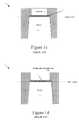
- the typical prior art processis shown in FIGS. 1 a through 1 e.
- a gate structure 1comprising a pad oxide layer, sandwiched between a pad nitride layer 3 and a silicon substrate 4 .
- Typical values of the pad nitride pullbackare from 0 to 30 nm.
- the nitride pullbackis done by using selective wet chemical etch of the pad nitride.
- the next steps in the processingare the oxidation of the exposed silicon (active area, or “AA”, oxidation) and an STI fill with a dielectric, usually oxide.
- the pad nitride 3is then stripped. This strip is selected to the oxide 5 , although it etches a small part of it. Typical etch selectivities are 1 to 50. For 100 nm of nitride that gives 2 nm of sideways oxide etch. This is followed by an etch of the pad oxide 2 . With some overetch, this etch also extends sideways into the STI isolation oxide 5 . For a typical pad oxide thickness of 5 nm, this gives a sideways etch of 5 to 7 nm. The pad oxide etch is followed by sacrificial oxidation to create a thin oxide with well-defined thickness and uniformity. This oxide is needed as a screen oxide for implants.
- the thickness of the sacrificial oxide 6is typically 5 nm to 10 nm.
- the sacrificial oxideis stripped using wet chemical oxide etch selective to nitride. Again using a slight overetch, approximately 10 nm of oxide are etched sideways into the STI. This sideways etch is sometimes even larger depending on the densification of the oxide used for the STI fill. This step leads to the exposure of the STI edge. In the following gate oxidation, the gate oxide 7 is usually thinner at the edges, especially the corners, as compared to the center. The reason is believed to be the orientation dependent oxidation rate and, to a larger extent, mechanical stress.
- a method of processing a semiconductor gate structure on a semiconductor wafercomprising providing a semiconductor structure comprising a semiconductor gate capped with a pad oxide layer bounded by one or more isolation trenches filled with silicon oxide, providing a sacrificial oxide layer by thickening said pad oxide layer to a thickness effective in using said thickened pad oxide layer as said sacrificial oxide layer, stripping said sacrificial pad oxide layer after use, and capping said semiconductor gate with a gate oxide layer.
- said thickening stepcomprises heating said semiconductor wafer in an oxygen-containing atmosphere to a temperature effective in silicon oxide growth.
- said semiconductor waferis heated to a temperature of from about 500° C. to about 1,000° C.
- said temperatureis about 700° C.
- said semiconductor waferis heated for about one hour.
- said sacrificial oxide layeris from about 20 to about 100 angstroms thick.
- said sacrificial oxide layeris from about 30 to about 50 angstroms thick.
- said sacrificial oxide layeris about 40 angstroms thick.
- said sacrificial oxide layercomprises amorphous silicon oxide.
- a semiconductor structurecomprising a semiconductor gate capped with a sacrificial oxide layer bounded by one or more isolation trenches, and said sacrificial oxide layer comprises amorphous silicon oxide.
- said sacrificial oxide layeris between about 20 to about 100 angstroms thick.
- said sacrificial oxide layeris between about 30 to about 50 angstroms thick.
- said sacrificial oxide layeris about 40 angstroms thick.
- FIGS. 1 a through 1 eshow the typical prior art method of manufacturing a gate.
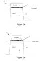
- FIGS. 2 a through 2 fshow the inventive method of manufacturing a gate.
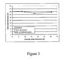
- FIG. 3shows a graph of final sacrificial oxide thickness versus starting pad oxide thickness.
- a basic idea of the present inventionis to reduce the number of oxide etch steps and therefore avoid the exposure of the STI corners.
- the basic steps of the inventionmay be summarized and compared to that described above with respect to the prior art, such as is shown in Table I, below.
- FIGS. 2 a through 2 care depicted identically to FIGS. 1 a through 1 c, excepting that different numerals are used.
- FIGS. 2 a through 2 cthere is shown a gate structure 10 having a pad oxide layer 20 sandwiched between a pad nitride layer 30 and a silicon substrate 40 , isolation trenches on either side of the gate structure 10 having been filled in with oxide 50 .
- silicon nitridehas been stripped away, but the pad oxide is left intact, resulting in a basic semiconductor structure comprising a semiconductor gate 10 capped with a pad oxide layer 20 bounded by one or more trench fills 50 .
- Preferred etches for silicon nitrideinclude phosphoric acid (H 3 PO 4 ) and sodium hydroxide (NaOH) isotropic wet etches, which are selective with respect to organic polymers, polysilicon, silicon, and metals. These etches are effected by immersing the wafer in an aqueous solution of NaOH or H 3 PO 4 at temperatures of generally 80° C. or more, preferably 100° C. or more, for ° C.
- sodium hydroxide etchesand generally 150° C. or more, preferably 180° C. or more, for phosphoric acid etches.
- concentration of etchantin solution with reflux.
- a number of chemical bath systemsare commercially available just for this purpose, such as those sold under the NITRAN brand name by Lufran, Inc., of Streetsboro, Ohio.
- FIG. 2 ethere is now a thick layer of oxide 60 upon the gate substrate 40 , which is thick enough to be used as a sacrificial oxide layer 60 .
- the manufacturermay now perform whatever implants and anneals are desired, followed by the stripping of the sacrificial oxide 60 by wet chemical etch.
- FIG. 2 fthere is shown the final gate oxide 70 that is thermally grown after stripping away of the sacrificial oxide 60 . Due to the elimination of the pad oxide strip (see prior art), the result is that the edges of the oxide show no substantial penetration into the surrounding trench fill 50 , though there will usually be some detectable, if unsubstantial, lateral widening.
- FIG. 3wherein there is shown a graph of final sacrificial oxide thickness versus starting pad oxide thickness.
- starting oxide thicknessis meant the thickness of the pad oxide 20 after the stripping of the pad nitride 30 , such as is shown in FIG. 2 d.
- the thickness of the pad oxide after pad nitride stripis dependent on the pad nitride uniformity and pad nitride etch uniformity, it typically shows large variations from wafer to wafer as well as on a wafer from center to edge.
- final thicknessis meant the measured thickness of the pad oxide layer after the thickening step as, now acting as sacrificial oxide 60 shown in FIG. 2 e. As can be seen, sacrificial oxide layer 60 thickness is maintained at about forty angstroms regardless of the starting thickness. Initial pad oxide thicknesses ranging from seven to thirty angstroms were used to generate this graph.
- the actual thickness chosenwill be a thickness effective in enabling the use of the oxide layer 60 as a sacrificial oxide for whatever implants, anneals, or other process steps the user has in mind. Generally, the thickness will be from 20 to 100 angstroms, more preferably from about 30 to about 80 angstroms for such purposes, but generally the thickness will be about 40 or 50 angstroms because the rate of reaction begins to fall off substantially at around 50 angstroms, thereby slowing the manufacturing process.
- the method of the inventionreplaces the pad oxide stripping step with an oxidation step and thereby significantly reduces lateral oxide etching of the surrounding trench fill by eliminating an etching step.
- high-k dielectricssuch as, for example, barium strontium titanate (BST), lead zirconate titanate (PZT) and lanthanam-doped PZT (PLZT).
Landscapes
- Engineering & Computer Science (AREA)
- Physics & Mathematics (AREA)
- Condensed Matter Physics & Semiconductors (AREA)
- General Physics & Mathematics (AREA)
- Manufacturing & Machinery (AREA)
- Computer Hardware Design (AREA)
- Microelectronics & Electronic Packaging (AREA)
- Power Engineering (AREA)
- Element Separation (AREA)
Abstract
Description
| TABLE I | |
| Inventive Method | |
| 1. STI dry etch through | 1. STI dry etch through |
| nitride, pad oxide, | pad nitride, pad oxide, |
| and to a predefined depth | and to a predefined |
| into the silicon. | depth into the silicon. |
| 2. Pad nitride pullback. | 2. Pad nitride pullback. |
| 3. AA oxidation. | 3. AA oxidation. |
| 4. STI oxide fill and planarization. | 4. STI oxide fill |
| and planarization. | |
| 5. Pad nitride strip. | 5. Pad nitride strip. |
| 6. Oxidation step to increase the thickness of | 6. Pad oxide strip. |
| the remaining pad oxide to the desired | 7. Sacrificial |
| oxide thickness. | oxide growth. |
| 8. Implants and anneals. | |
| 7. Implants and anneals. | 9. Sacrificial oxide strip. |
| 8. Sacrificial oxide strip. | 10. Gate oxidation. |
| 9. Gate oxidation. | |
Claims (8)
Priority Applications (2)
| Application Number | Priority Date | Filing Date | Title |
|---|---|---|---|
| US09/965,919US6656798B2 (en) | 2001-09-28 | 2001-09-28 | Gate processing method with reduced gate oxide corner and edge thinning |
| DE10244569ADE10244569B4 (en) | 2001-09-28 | 2002-09-25 | Gate processing with reduced gate oxide corner and edge thinning |
Applications Claiming Priority (1)
| Application Number | Priority Date | Filing Date | Title |
|---|---|---|---|
| US09/965,919US6656798B2 (en) | 2001-09-28 | 2001-09-28 | Gate processing method with reduced gate oxide corner and edge thinning |
Publications (2)
| Publication Number | Publication Date |
|---|---|
| US20030067035A1 US20030067035A1 (en) | 2003-04-10 |
| US6656798B2true US6656798B2 (en) | 2003-12-02 |
Family
ID=25510675
Family Applications (1)
| Application Number | Title | Priority Date | Filing Date |
|---|---|---|---|
| US09/965,919Expired - LifetimeUS6656798B2 (en) | 2001-09-28 | 2001-09-28 | Gate processing method with reduced gate oxide corner and edge thinning |
Country Status (2)
| Country | Link |
|---|---|
| US (1) | US6656798B2 (en) |
| DE (1) | DE10244569B4 (en) |
Cited By (1)
| Publication number | Priority date | Publication date | Assignee | Title |
|---|---|---|---|---|
| US20070063277A1 (en)* | 2005-09-22 | 2007-03-22 | International Business Machines Corporation | Multiple low and high k gate oxides on single gate for lower miller capacitance and improved drive current |
Families Citing this family (67)
| Publication number | Priority date | Publication date | Assignee | Title |
|---|---|---|---|---|
| US7388259B2 (en)* | 2002-11-25 | 2008-06-17 | International Business Machines Corporation | Strained finFET CMOS device structures |
| US7091104B2 (en)* | 2003-01-23 | 2006-08-15 | Silterra Malaysia Sdn. Bhd. | Shallow trench isolation |
| US6887798B2 (en) | 2003-05-30 | 2005-05-03 | International Business Machines Corporation | STI stress modification by nitrogen plasma treatment for improving performance in small width devices |
| US7410846B2 (en)* | 2003-09-09 | 2008-08-12 | International Business Machines Corporation | Method for reduced N+ diffusion in strained Si on SiGe substrate |
| US6890808B2 (en)* | 2003-09-10 | 2005-05-10 | International Business Machines Corporation | Method and structure for improved MOSFETs using poly/silicide gate height control |
| US6887751B2 (en)* | 2003-09-12 | 2005-05-03 | International Business Machines Corporation | MOSFET performance improvement using deformation in SOI structure |
| US7170126B2 (en) | 2003-09-16 | 2007-01-30 | International Business Machines Corporation | Structure of vertical strained silicon devices |
| US7144767B2 (en)* | 2003-09-23 | 2006-12-05 | International Business Machines Corporation | NFETs using gate induced stress modulation |
| US7119403B2 (en)* | 2003-10-16 | 2006-10-10 | International Business Machines Corporation | High performance strained CMOS devices |
| US7303949B2 (en) | 2003-10-20 | 2007-12-04 | International Business Machines Corporation | High performance stress-enhanced MOSFETs using Si:C and SiGe epitaxial source/drain and method of manufacture |
| US7037770B2 (en)* | 2003-10-20 | 2006-05-02 | International Business Machines Corporation | Method of manufacturing strained dislocation-free channels for CMOS |
| US7129126B2 (en)* | 2003-11-05 | 2006-10-31 | International Business Machines Corporation | Method and structure for forming strained Si for CMOS devices |
| US7015082B2 (en)* | 2003-11-06 | 2006-03-21 | International Business Machines Corporation | High mobility CMOS circuits |
| US7029964B2 (en) | 2003-11-13 | 2006-04-18 | International Business Machines Corporation | Method of manufacturing a strained silicon on a SiGe on SOI substrate |
| US7122849B2 (en)* | 2003-11-14 | 2006-10-17 | International Business Machines Corporation | Stressed semiconductor device structures having granular semiconductor material |
| US7247534B2 (en) | 2003-11-19 | 2007-07-24 | International Business Machines Corporation | Silicon device on Si:C-OI and SGOI and method of manufacture |
| US7198995B2 (en) | 2003-12-12 | 2007-04-03 | International Business Machines Corporation | Strained finFETs and method of manufacture |
| US7247912B2 (en)* | 2004-01-05 | 2007-07-24 | International Business Machines Corporation | Structures and methods for making strained MOSFETs |
| US7118999B2 (en)* | 2004-01-16 | 2006-10-10 | International Business Machines Corporation | Method and apparatus to increase strain effect in a transistor channel |
| US7202132B2 (en) | 2004-01-16 | 2007-04-10 | International Business Machines Corporation | Protecting silicon germanium sidewall with silicon for strained silicon/silicon germanium MOSFETs |
| US7381609B2 (en) | 2004-01-16 | 2008-06-03 | International Business Machines Corporation | Method and structure for controlling stress in a transistor channel |
| US7923782B2 (en)* | 2004-02-27 | 2011-04-12 | International Business Machines Corporation | Hybrid SOI/bulk semiconductor transistors |
| US7205206B2 (en)* | 2004-03-03 | 2007-04-17 | International Business Machines Corporation | Method of fabricating mobility enhanced CMOS devices |
| US7504693B2 (en) | 2004-04-23 | 2009-03-17 | International Business Machines Corporation | Dislocation free stressed channels in bulk silicon and SOI CMOS devices by gate stress engineering |
| US7223994B2 (en)* | 2004-06-03 | 2007-05-29 | International Business Machines Corporation | Strained Si on multiple materials for bulk or SOI substrates |
| US7037794B2 (en) | 2004-06-09 | 2006-05-02 | International Business Machines Corporation | Raised STI process for multiple gate ox and sidewall protection on strained Si/SGOI structure with elevated source/drain |
| US7227205B2 (en) | 2004-06-24 | 2007-06-05 | International Business Machines Corporation | Strained-silicon CMOS device and method |
| TWI463526B (en) | 2004-06-24 | 2014-12-01 | Ibm | Method for improving stress-induced CMOS components and components prepared by the method |
| US7288443B2 (en)* | 2004-06-29 | 2007-10-30 | International Business Machines Corporation | Structures and methods for manufacturing p-type MOSFET with graded embedded silicon-germanium source-drain and/or extension |
| US7217949B2 (en)* | 2004-07-01 | 2007-05-15 | International Business Machines Corporation | Strained Si MOSFET on tensile-strained SiGe-on-insulator (SGOI) |
| US6991998B2 (en)* | 2004-07-02 | 2006-01-31 | International Business Machines Corporation | Ultra-thin, high quality strained silicon-on-insulator formed by elastic strain transfer |
| US7384829B2 (en) | 2004-07-23 | 2008-06-10 | International Business Machines Corporation | Patterned strained semiconductor substrate and device |
| US7238565B2 (en) | 2004-12-08 | 2007-07-03 | International Business Machines Corporation | Methodology for recovery of hot carrier induced degradation in bipolar devices |
| US7262087B2 (en) | 2004-12-14 | 2007-08-28 | International Business Machines Corporation | Dual stressed SOI substrates |
| US7173312B2 (en)* | 2004-12-15 | 2007-02-06 | International Business Machines Corporation | Structure and method to generate local mechanical gate stress for MOSFET channel mobility modification |
| US7274084B2 (en)* | 2005-01-12 | 2007-09-25 | International Business Machines Corporation | Enhanced PFET using shear stress |
| US20060160317A1 (en)* | 2005-01-18 | 2006-07-20 | International Business Machines Corporation | Structure and method to enhance stress in a channel of cmos devices using a thin gate |
| US7432553B2 (en)* | 2005-01-19 | 2008-10-07 | International Business Machines Corporation | Structure and method to optimize strain in CMOSFETs |
| US7220626B2 (en)* | 2005-01-28 | 2007-05-22 | International Business Machines Corporation | Structure and method for manufacturing planar strained Si/SiGe substrate with multiple orientations and different stress levels |
| US7256081B2 (en)* | 2005-02-01 | 2007-08-14 | International Business Machines Corporation | Structure and method to induce strain in a semiconductor device channel with stressed film under the gate |
| US7224033B2 (en) | 2005-02-15 | 2007-05-29 | International Business Machines Corporation | Structure and method for manufacturing strained FINFET |
| US7545004B2 (en)* | 2005-04-12 | 2009-06-09 | International Business Machines Corporation | Method and structure for forming strained devices |
| US7544577B2 (en)* | 2005-08-26 | 2009-06-09 | International Business Machines Corporation | Mobility enhancement in SiGe heterojunction bipolar transistors |
| US7202513B1 (en)* | 2005-09-29 | 2007-04-10 | International Business Machines Corporation | Stress engineering using dual pad nitride with selective SOI device architecture |
| US20070096170A1 (en)* | 2005-11-02 | 2007-05-03 | International Business Machines Corporation | Low modulus spacers for channel stress enhancement |
| US7655511B2 (en) | 2005-11-03 | 2010-02-02 | International Business Machines Corporation | Gate electrode stress control for finFET performance enhancement |
| US7785950B2 (en)* | 2005-11-10 | 2010-08-31 | International Business Machines Corporation | Dual stress memory technique method and related structure |
| US7709317B2 (en) | 2005-11-14 | 2010-05-04 | International Business Machines Corporation | Method to increase strain enhancement with spacerless FET and dual liner process |
| US7348638B2 (en)* | 2005-11-14 | 2008-03-25 | International Business Machines Corporation | Rotational shear stress for charge carrier mobility modification |
| US7564081B2 (en) | 2005-11-30 | 2009-07-21 | International Business Machines Corporation | finFET structure with multiply stressed gate electrode |
| US7776695B2 (en)* | 2006-01-09 | 2010-08-17 | International Business Machines Corporation | Semiconductor device structure having low and high performance devices of same conductive type on same substrate |
| US7863197B2 (en) | 2006-01-09 | 2011-01-04 | International Business Machines Corporation | Method of forming a cross-section hourglass shaped channel region for charge carrier mobility modification |
| US7635620B2 (en) | 2006-01-10 | 2009-12-22 | International Business Machines Corporation | Semiconductor device structure having enhanced performance FET device |
| US20070158743A1 (en)* | 2006-01-11 | 2007-07-12 | International Business Machines Corporation | Thin silicon single diffusion field effect transistor for enhanced drive performance with stress film liners |
| US7691698B2 (en) | 2006-02-21 | 2010-04-06 | International Business Machines Corporation | Pseudomorphic Si/SiGe/Si body device with embedded SiGe source/drain |
| US8461009B2 (en)* | 2006-02-28 | 2013-06-11 | International Business Machines Corporation | Spacer and process to enhance the strain in the channel with stress liner |
| US7615418B2 (en)* | 2006-04-28 | 2009-11-10 | International Business Machines Corporation | High performance stress-enhance MOSFET and method of manufacture |
| US7521307B2 (en)* | 2006-04-28 | 2009-04-21 | International Business Machines Corporation | CMOS structures and methods using self-aligned dual stressed layers |
| US7608489B2 (en)* | 2006-04-28 | 2009-10-27 | International Business Machines Corporation | High performance stress-enhance MOSFET and method of manufacture |
| US8853746B2 (en) | 2006-06-29 | 2014-10-07 | International Business Machines Corporation | CMOS devices with stressed channel regions, and methods for fabricating the same |
| US7790540B2 (en) | 2006-08-25 | 2010-09-07 | International Business Machines Corporation | Structure and method to use low k stress liner to reduce parasitic capacitance |
| US7462522B2 (en)* | 2006-08-30 | 2008-12-09 | International Business Machines Corporation | Method and structure for improving device performance variation in dual stress liner technology |
| US8754446B2 (en) | 2006-08-30 | 2014-06-17 | International Business Machines Corporation | Semiconductor structure having undercut-gate-oxide gate stack enclosed by protective barrier material |
| US8115254B2 (en) | 2007-09-25 | 2012-02-14 | International Business Machines Corporation | Semiconductor-on-insulator structures including a trench containing an insulator stressor plug and method of fabricating same |
| US8492846B2 (en) | 2007-11-15 | 2013-07-23 | International Business Machines Corporation | Stress-generating shallow trench isolation structure having dual composition |
| US8598006B2 (en)* | 2010-03-16 | 2013-12-03 | International Business Machines Corporation | Strain preserving ion implantation methods |
| US11502106B2 (en)* | 2020-02-11 | 2022-11-15 | Globalfoundries U.S. Inc. | Multi-layered substrates of semiconductor devices |
Citations (5)
| Publication number | Priority date | Publication date | Assignee | Title |
|---|---|---|---|---|
| US6087243A (en)* | 1997-10-21 | 2000-07-11 | Advanced Micro Devices, Inc. | Method of forming trench isolation with high integrity, ultra thin gate oxide |
| US6309924B1 (en)* | 2000-06-02 | 2001-10-30 | International Business Machines Corporation | Method of forming self-limiting polysilicon LOCOS for DRAM cell |
| US6342431B2 (en)* | 1998-10-14 | 2002-01-29 | International Business Machines Corporation | Method for eliminating transfer gate sacrificial oxide |
| US6391720B1 (en)* | 2000-09-27 | 2002-05-21 | Chartered Semiconductor Manufacturing Ltd. | Process flow for a performance enhanced MOSFET with self-aligned, recessed channel |
| US6437381B1 (en)* | 2000-04-27 | 2002-08-20 | International Business Machines Corporation | Semiconductor memory device with reduced orientation-dependent oxidation in trench structures |
Family Cites Families (1)
| Publication number | Priority date | Publication date | Assignee | Title |
|---|---|---|---|---|
| US6194285B1 (en)* | 1999-10-04 | 2001-02-27 | Taiwan Semiconductor Manufacturing Company | Formation of shallow trench isolation (STI) |
- 2001
- 2001-09-28USUS09/965,919patent/US6656798B2/ennot_activeExpired - Lifetime
- 2002
- 2002-09-25DEDE10244569Apatent/DE10244569B4/ennot_activeExpired - Lifetime
Patent Citations (5)
| Publication number | Priority date | Publication date | Assignee | Title |
|---|---|---|---|---|
| US6087243A (en)* | 1997-10-21 | 2000-07-11 | Advanced Micro Devices, Inc. | Method of forming trench isolation with high integrity, ultra thin gate oxide |
| US6342431B2 (en)* | 1998-10-14 | 2002-01-29 | International Business Machines Corporation | Method for eliminating transfer gate sacrificial oxide |
| US6437381B1 (en)* | 2000-04-27 | 2002-08-20 | International Business Machines Corporation | Semiconductor memory device with reduced orientation-dependent oxidation in trench structures |
| US6309924B1 (en)* | 2000-06-02 | 2001-10-30 | International Business Machines Corporation | Method of forming self-limiting polysilicon LOCOS for DRAM cell |
| US6391720B1 (en)* | 2000-09-27 | 2002-05-21 | Chartered Semiconductor Manufacturing Ltd. | Process flow for a performance enhanced MOSFET with self-aligned, recessed channel |
Cited By (1)
| Publication number | Priority date | Publication date | Assignee | Title |
|---|---|---|---|---|
| US20070063277A1 (en)* | 2005-09-22 | 2007-03-22 | International Business Machines Corporation | Multiple low and high k gate oxides on single gate for lower miller capacitance and improved drive current |
Also Published As
| Publication number | Publication date |
|---|---|
| DE10244569A1 (en) | 2003-04-24 |
| DE10244569B4 (en) | 2006-08-10 |
| US20030067035A1 (en) | 2003-04-10 |
Similar Documents
| Publication | Publication Date | Title |
|---|---|---|
| US6656798B2 (en) | Gate processing method with reduced gate oxide corner and edge thinning | |
| US6746936B1 (en) | Method for forming isolation film for semiconductor devices | |
| US7696045B2 (en) | Method of manufacturing semiconductor device | |
| JP4825402B2 (en) | Manufacturing method of semiconductor device | |
| EP0624899A2 (en) | Oxidation of silicon nitride in semiconductor devices | |
| US6953727B2 (en) | Manufacture method of semiconductor device with gate insulating films of different thickness | |
| US6472324B2 (en) | Method of manufacturing trench type element isolation structure | |
| US6346457B1 (en) | Process for manufacturing semiconductor device | |
| JP5326361B2 (en) | Manufacturing method of semiconductor device | |
| US20050189609A1 (en) | Embedded semiconductor product with dual depth isolation regions | |
| US6989318B2 (en) | Method for reducing shallow trench isolation consumption in semiconductor devices | |
| KR101054320B1 (en) | Method for manufacturing semiconductor device | |
| US20030232503A1 (en) | Method for manufacturing semiconductor device | |
| US7186632B2 (en) | Method of fabricating a semiconductor device having a decreased concentration of phosphorus impurities in polysilicon | |
| KR100381849B1 (en) | Trench isolation method | |
| US6734526B1 (en) | Oxidation resistant microelectronics capacitor structure with L shaped isolation spacer | |
| US20060030118A1 (en) | Method of manufacturing a semiconductor device with field isolation regions consisting of grooves filled with isolation material | |
| US6743690B2 (en) | Method of forming a metal-oxide semiconductor transistor | |
| US6887767B2 (en) | Method for manufacturing semiconductor device | |
| KR0167252B1 (en) | Device isolation method of semiconductor integrated circuit | |
| CN1770402A (en) | Fabrication method of gate oxide layer | |
| JPH1050693A (en) | Method for manufacturing semiconductor device | |
| CN107978606A (en) | A kind of embedded flash memory technology integrating method | |
| KR100274350B1 (en) | Method of forming a field oxide firm in a semiconductor device | |
| JP2003051536A (en) | Wafer treatment method and production method for semiconductor device |
Legal Events
| Date | Code | Title | Description |
|---|---|---|---|
| AS | Assignment | Owner name:INFINEON TECHNOLOGIES NORTH AMERICA CORP., CALIFOR Free format text:ASSIGNMENT OF ASSIGNORS INTEREST;ASSIGNOR:TEWS, HELMUT;REEL/FRAME:012468/0642 Effective date:20011109 | |
| AS | Assignment | Owner name:INTERNATIONAL BUSINESS MACHINES CORPORATION, NEW Y Free format text:ASSIGNMENT OF ASSIGNORS INTEREST;ASSIGNORS:GLUSCHENKOV, OLEG;WEYBRIGHT, MARY;REEL/FRAME:012468/0633;SIGNING DATES FROM 20011107 TO 20011109 | |
| AS | Assignment | Owner name:INFINEON TECHNOLOGIES AG, GERMANY Free format text:ASSIGNMENT OF ASSIGNORS INTEREST;ASSIGNOR:INFINEON TECHNOLOGIES NORTH AMERICA CORP.;REEL/FRAME:013287/0681 Effective date:20020828 | |
| STCF | Information on status: patent grant | Free format text:PATENTED CASE | |
| FPAY | Fee payment | Year of fee payment:4 | |
| AS | Assignment | Owner name:QIMONDA AG, GERMANY Free format text:ASSIGNMENT OF ASSIGNORS INTEREST;ASSIGNOR:INFINEON TECHNOLOGIES AG;REEL/FRAME:023788/0535 Effective date:20060425 | |
| FPAY | Fee payment | Year of fee payment:8 | |
| AS | Assignment | Owner name:INFINEON TECHNOLOGIES AG, GERMANY Free format text:ASSIGNMENT OF ASSIGNORS INTEREST;ASSIGNOR:QIMONDA AG;REEL/FRAME:035623/0001 Effective date:20141009 | |
| FPAY | Fee payment | Year of fee payment:12 | |
| AS | Assignment | Owner name:GLOBALFOUNDRIES U.S. 2 LLC, NEW YORK Free format text:ASSIGNMENT OF ASSIGNORS INTEREST;ASSIGNOR:INTERNATIONAL BUSINESS MACHINES CORPORATION;REEL/FRAME:036550/0001 Effective date:20150629 | |
| AS | Assignment | Owner name:GLOBALFOUNDRIES INC., CAYMAN ISLANDS Free format text:ASSIGNMENT OF ASSIGNORS INTEREST;ASSIGNORS:GLOBALFOUNDRIES U.S. 2 LLC;GLOBALFOUNDRIES U.S. INC.;REEL/FRAME:036779/0001 Effective date:20150910 | |
| AS | Assignment | Owner name:SAMSUNG ELECTRONICS CO., LTD., KOREA, REPUBLIC OF Free format text:ASSIGNMENT OF ASSIGNORS INTEREST;ASSIGNOR:INFINEON TECHNOLOGIES AG;REEL/FRAME:037221/0885 Effective date:20150930 | |
| AS | Assignment | Owner name:WILMINGTON TRUST, NATIONAL ASSOCIATION, DELAWARE Free format text:SECURITY AGREEMENT;ASSIGNOR:GLOBALFOUNDRIES INC.;REEL/FRAME:049490/0001 Effective date:20181127 | |
| AS | Assignment | Owner name:GLOBALFOUNDRIES U.S. INC., CALIFORNIA Free format text:ASSIGNMENT OF ASSIGNORS INTEREST;ASSIGNOR:GLOBALFOUNDRIES INC.;REEL/FRAME:054633/0001 Effective date:20201022 | |
| AS | Assignment | Owner name:GLOBALFOUNDRIES INC., CAYMAN ISLANDS Free format text:RELEASE BY SECURED PARTY;ASSIGNOR:WILMINGTON TRUST, NATIONAL ASSOCIATION;REEL/FRAME:054636/0001 Effective date:20201117 | |
| AS | Assignment | Owner name:GLOBALFOUNDRIES U.S. INC., NEW YORK Free format text:RELEASE BY SECURED PARTY;ASSIGNOR:WILMINGTON TRUST, NATIONAL ASSOCIATION;REEL/FRAME:056987/0001 Effective date:20201117 |