US6656761B2 - Method for forming a semiconductor device for detecting light - Google Patents
Method for forming a semiconductor device for detecting lightDownload PDFInfo
- Publication number
- US6656761B2 US6656761B2US09/990,977US99097701AUS6656761B2US 6656761 B2US6656761 B2US 6656761B2US 99097701 AUS99097701 AUS 99097701AUS 6656761 B2US6656761 B2US 6656761B2
- Authority
- US
- United States
- Prior art keywords
- reflective
- layer
- reflective stack
- silicon
- stack
- Prior art date
- Legal status (The legal status is an assumption and is not a legal conclusion. Google has not performed a legal analysis and makes no representation as to the accuracy of the status listed.)
- Expired - Lifetime
Links
Images


Classifications
- H—ELECTRICITY
- H10—SEMICONDUCTOR DEVICES; ELECTRIC SOLID-STATE DEVICES NOT OTHERWISE PROVIDED FOR
- H10F—INORGANIC SEMICONDUCTOR DEVICES SENSITIVE TO INFRARED RADIATION, LIGHT, ELECTROMAGNETIC RADIATION OF SHORTER WAVELENGTH OR CORPUSCULAR RADIATION
- H10F30/00—Individual radiation-sensitive semiconductor devices in which radiation controls the flow of current through the devices, e.g. photodetectors
- H10F30/20—Individual radiation-sensitive semiconductor devices in which radiation controls the flow of current through the devices, e.g. photodetectors the devices having potential barriers, e.g. phototransistors
- H10F30/21—Individual radiation-sensitive semiconductor devices in which radiation controls the flow of current through the devices, e.g. photodetectors the devices having potential barriers, e.g. phototransistors the devices being sensitive to infrared, visible or ultraviolet radiation
- H10F30/22—Individual radiation-sensitive semiconductor devices in which radiation controls the flow of current through the devices, e.g. photodetectors the devices having potential barriers, e.g. phototransistors the devices being sensitive to infrared, visible or ultraviolet radiation the devices having only one potential barrier, e.g. photodiodes
- H—ELECTRICITY
- H10—SEMICONDUCTOR DEVICES; ELECTRIC SOLID-STATE DEVICES NOT OTHERWISE PROVIDED FOR
- H10F—INORGANIC SEMICONDUCTOR DEVICES SENSITIVE TO INFRARED RADIATION, LIGHT, ELECTROMAGNETIC RADIATION OF SHORTER WAVELENGTH OR CORPUSCULAR RADIATION
- H10F71/00—Manufacture or treatment of devices covered by this subclass
- H—ELECTRICITY
- H10—SEMICONDUCTOR DEVICES; ELECTRIC SOLID-STATE DEVICES NOT OTHERWISE PROVIDED FOR
- H10F—INORGANIC SEMICONDUCTOR DEVICES SENSITIVE TO INFRARED RADIATION, LIGHT, ELECTROMAGNETIC RADIATION OF SHORTER WAVELENGTH OR CORPUSCULAR RADIATION
- H10F77/00—Constructional details of devices covered by this subclass
- H10F77/30—Coatings
- H10F77/306—Coatings for devices having potential barriers
- H—ELECTRICITY
- H10—SEMICONDUCTOR DEVICES; ELECTRIC SOLID-STATE DEVICES NOT OTHERWISE PROVIDED FOR
- H10F—INORGANIC SEMICONDUCTOR DEVICES SENSITIVE TO INFRARED RADIATION, LIGHT, ELECTROMAGNETIC RADIATION OF SHORTER WAVELENGTH OR CORPUSCULAR RADIATION
- H10F77/00—Constructional details of devices covered by this subclass
- H10F77/40—Optical elements or arrangements
- H10F77/413—Optical elements or arrangements directly associated or integrated with the devices, e.g. back reflectors
Definitions
- the present inventionrelates to the field of semiconductor processing and, more particularly, to optoelectronic devices.
- a continuing object of integrated circuit manufacturingis to increase the speed of operation.
- One obstacleis the speed at which signals for the source of information are sent to the integrated circuit.
- Optical devicesare being investigated to increase the speed of operation by using light as opposed to an electrical signal as the source.
- a resonant cavity detectorincludes, two mirrors or distributed Bragg reflectors (DBR) vertically separated from each other by a silicon layer. When light is applied to the resonant cavity device the mirrors bounce the light between each other and multiply the light intensity. The greater the light intensity the more number of electron and hole pairs will be formed in the silicon to transmit a signal.
- DBRdistributed Bragg reflector
- the silicon layer between the two mirrorsis polysilicon, the current flowing in the absence of radiation (dark current) is large, which decreases the efficiency of the device.
- monocrystalline siliconhas a low dark current and is therefore used as the silicon layer in resonant cavity devices.
- One way the prior art forms a resonant cavity device with a monocrystalline silicon layer between the mirrorsis to form the bottom mirror, etch two holes within the bottom mirror to expose the underlying silicon substrate and epitaxially grow silicon through the two holes and laterally across the top surface of the bottom mirror. Afterwards, the upper mirror is formed within the epitaxially grown silicon. By growing the semiconductor material laterally across the top surface of the bottom mirror the semiconductor material also grows vertically to a thickness much greater than desired. To reduce the thickness of the epitaxial layer, a chemical mechanical polish (CMP) or etch back step is needed. This process is undesirable for manufacturability because the epitaxial growth process is slow and the CMP or etch back step increases cycle time by adding additional steps.
- CMPchemical mechanical polish
- the epitaxial growthintroduces defects in the epitaxially grown silicon at the locations where the lateral overgrowth of the silicon meets over the top surface of the mirror.
- a more manufacturable process to form a monocrystalline semiconductor material between two mirrors in an optical deviceis needed.
- FIGS. 1-4illustrate cross-sectional views of a portion of a semiconductor substrate during a process flow to form a resonant cavity device in accordance with an embodiment of the present invention
- FIG. 5illustrates an alternate embodiment of FIG. 4 also in accordance with the present invention.
- a method of forming a resonant cavity device useful for optoelectronic applicationsis formed by wafer bonding a semiconductor material, such as a silicon-comprising material, to a stack of reflective layers formed over a semiconductor substrate.
- the resonant cavity devicecan be formed on a semiconductor substrate before the formation of a transistor.
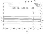
- FIG. 1illustrates a portion of a semiconductor device 10 including a first semiconductor substrate 12 and a bottom reflective stack or bottom mirror 15 that includes first reflective layers 14 and second reflective layers 16 .
- the first semiconductor substrate 12can be any semiconductor material and is preferably a silicon-comprising wafer, such as a silicon monocrystalline wafer.
- a mirrorreflects a desired wavelength of light, wherein a desired wavelength of light is the wavelength of light that carries information and is captured by a photodetector.
- the desired wavelengths of lightare most typically 850 nanometers, 1310 nanometers, and 1510 nanometers.
- a reflective stackis a stack of alternating layers of materials having different refractive indices, which together function as a mirror. Each layer has a thickness within the reflective stack that is dependent upon 1) the wavelength of light that will subsequently be applied to the semiconductor device 10 and 2) the refractive index of the material in accordance with equation 1.
- tis the thickness of the layer
- ⁇is the wavelength of the incident light
- nis the index of refraction of the material.
- the desired wavelength of lightis approximately 850 nanometers; for metropolitan area network (MAN) applications (approximately 10 km), the wavelength is 1310 nanometers and for wide area networks (WAN) applications (approximately 40-100 km), the desired wavelength is approximately 1510 nanometers.
- MANmetropolitan area network
- WANwide area networks
- a reflective stack 15 of silicon dioxide (SiO 2 ) and polysiliconis used. Because the index of refraction for silicon dioxide is approximately 1.4, the SiO 2 layer is about 146 nanometers. Polysilicon has an index of refraction of approximately 3.6, and, thus, the thickness of the polysilicon layer is about 54 nanometers.
- the reflective stack 15 and the corresponding layers above and below the reflective stackmust have alternating indices of refraction with the layers above and below the reflective stack being a material with a higher index of refraction relative to the layer of the reflective stack that is in contact with them.
- the reflective stack 15is formed between layers of monocrystalline silicon, which has an index of refraction approximately equal to that of polysilicon.
- the bottom-most and top-most layers in the reflective stack 15which in FIG. 1 are the first reflective layer 14 , should have an index of refraction less than that of monocrystalline silicon and the second reflective layers 16 . Therefore, silicon dioxide is a suitable material for the first reflective layers 14 , and polysilicon is a suitable material for the second reflective layers 16 .
- the first reflective layercould be SiO 2 and the second reflective layer could be a nitride such as silicon nitride.
- the layers of the bottom reflective stack 15can be formed by thermal growth, CVD (chemical vapor deposition), PVD (physical vapor deposition), ALD (atomic layer deposition), the like or combinations of the above. However, it is not necessary that each layer be formed by the same process.
- the first reflective layer 14 in contact with the first silicon substrate 12can be a thermally grown SiO 2 layer. Afterwards, all the second reflective layers 16 and the remaining first reflective layers 14 can be formed by CVD, for example.
- the number of alternating layers within the bottom reflective stack 15can vary. Five layers are shown in the FIG. 2 for illustrative purposes only. However, the bottom reflective stack 15 has at least two layers of alternating materials. When the layers above and below the reflective stack are monocrystalline silicon, the number of layers in the bottom reflective stack 15 will be odd in order to achieve the necessary reflection characteristics. Also note that in one embodiment, the bottom reflective stack 15 may be inlaid within the first semiconductor substrate 12 .
- FIG. 2illustrates the semiconductor device 10 and a separate second semiconductor substrate or semiconductor layer 22 prior to wafer bonding.
- the semiconductor layer 22can be any semiconductor material, such as a silicon-comprising material and preferably is a silicon monocrystalline wafer.
- the second semiconductor substrate 22can be the same material or a different material than the first semiconductor substrate 12 .
- the second substrate 22can be bonded to the semiconductor device 10 by pressing the second semiconductor substrate 22 together with the semiconductor device 10 at a high temperature. Approximately 1000° C. to 1200° C. is useful for the high temperature. In addition, this temperature range can be used to anneal the wafers after pressing them together to increase the strength of the bonds, if desired.
- the anneal timeis usually on an order of magnitude of a couple of hours. For example, the anneal time may be between one to five hours. Other temperatures and anneal times may be used.
- a portion of the second substrate 22may be removed, if needed, by grinding, polishing or a cleaving process to form the desired thickness of the monocrystalline layer over the bottom reflective stack 15 .
- this desired thicknessmay be in a range of approximately 0.5 microns to 10 microns, or, alternatively, in a range of approximately 0.5 microns to 5 microns. Therefore, the desired thickness may be any thickness that results in a resonant cavity. For example, in one embodiment, the desired thickness may be approximately 1 micron.
- the resulting semiconductor device 10(without the optional thinning) is shown in FIG. 3 .
- any wafer bonding processingcan be used to bond a semiconductor substrate to the reflective stack, such as, for example, those described in U.S. Pat. No. 6,312,797, U.S. Pat. No. 6,284,629, and U.S. Pat. No. 6,180,496.
- the present inventionis not limited by the process used for wafer bonding or, if necessary, cleaving.
- FIG. 4shows the semiconductor device 10 after the formation of a top reflective stack 32 over the second semiconductor substrate 22 .
- first, electrodes 24 and 26are formed within a top portion of the semiconductor layer 22 .
- N type electrodes 24are formed by depositing a first photoresist layer (not shown), patterning the first photoresist layer and performing an N-type ion implantation using the first photoresist layer as an implant mask.
- P-type electrodes 26are formed by removing the first photoresist layer, forming a second photoresist layer, patterning the second photoresist layer, and performing a P-type ion implantation process using the second photoresist layer as an implant mask.
- the electrodes 24can be P-type and the electrodes 26 can be N-type.
- the electrodes 24 and 26can also be formed during the formation of source and drain regions for transistors formed on other areas of the semiconductor device 10 . Such transistor fabrication is well known in the art and therefore will not be described.
- the ion implantation doses and energies that are conventially used for forming the source and drains of the transistorscan be used for forming the electrodes 24 and 26 .
- a silicidation processcan be performed, where a salicide is formed over the source and drain regions and electrodes 24 and 26 .
- silicidationis not necessary and the electrode instead can be masked during silicidation of the source and drain regions to avoid silicidation.
- the top mirror or top reflective stack 32is formed.
- the top reflective stack 32is also an alternating stack of materials with different refractive indices, like the bottom reflective stack 15 .
- the top reflective stack 32includes a third reflective layer 28 and a fourth reflective layer 30 .
- the third reflective layer 28can be the same material as the first reflective layer 14 in the bottom reflective stack 15 and the fourth reflective layer 30 can be the same material as the second reflective layer 16 in the bottom reflective stack 15 . However, it is not necessary the same materials be used.
- the top reflective stack 32generally reflects less light than the bottom reflective stack 15 in order to maximize the light entering the optical device 10 .
- the top reflective stack 32reflects approximately 30 percent of incident light and the bottom reflective stack 15 reflects approximately 95 percent of incident light. This can be achieved by having fewer layers in the top reflective stack 32 as compared to the bottom reflective stack 15 .
- the number of layers for the top reflective stack 32 in FIG. 4is for illustrative purposes only, there are at least two layers of alternating materials.
- the materials over and under the top reflective stack 32should have indices of refraction greater than the layers of the top-reflective stack 32 they are in contact with.
- any processcan be used to form the third reflective layer 28 and the fourth reflective layer 30 such as thermal growth, CVD, PVD, ALD, combinations of the above or the like. Again, it is not necessary that each layer be formed by the same process.
- CMOSComplementary Metal-Oxide-Semiconductor
- processingmay be continued to form the gate electrodes for transistors and metal interconnects, for example.
- the semiconductor device 10is a resonant cavity device.
- FIG. 5shows an alternate embodiment of forming the top reflective stack 32 , where the top reflective stack 32 is inlaid, meaning at least a portion of the top reflective stack 32 lies within the second semiconductor substrate 22 .
- a trenchis etched in the second semiconductor substrate 22 .
- the electrodes 24 and 26are formed as previously described.
- the third and fourth reflective layer 28 and 30are formed within at least a portion of the trench by thermal growth, CVD, PVD, ALD, the like and combinations of the above. Portions of the third and fourth reflective layers 28 and 30 may lie outside the trench and can be removed by CMP or an etch process.
- FIG. 5shows all the layers of the top reflective stack 32 within the trench, some of the layers may lie within the trench and others over and outside the trench.
- a resonant cavity device using the described processesis a simple process, easily manufacturable, and compatible with existing semiconductor technology and fabrication processes.
- the quality of the semiconductor material between the reflective stacksis improved over materials formed by other techniques, such as a lateral epitaxial growth material.
Landscapes
- Led Devices (AREA)
Abstract
Description
Claims (9)
Priority Applications (1)
| Application Number | Priority Date | Filing Date | Title |
|---|---|---|---|
| US09/990,977US6656761B2 (en) | 2001-11-21 | 2001-11-21 | Method for forming a semiconductor device for detecting light |
Applications Claiming Priority (1)
| Application Number | Priority Date | Filing Date | Title |
|---|---|---|---|
| US09/990,977US6656761B2 (en) | 2001-11-21 | 2001-11-21 | Method for forming a semiconductor device for detecting light |
Publications (2)
| Publication Number | Publication Date |
|---|---|
| US20030096440A1 US20030096440A1 (en) | 2003-05-22 |
| US6656761B2true US6656761B2 (en) | 2003-12-02 |
Family
ID=25536712
Family Applications (1)
| Application Number | Title | Priority Date | Filing Date |
|---|---|---|---|
| US09/990,977Expired - LifetimeUS6656761B2 (en) | 2001-11-21 | 2001-11-21 | Method for forming a semiconductor device for detecting light |
Country Status (1)
| Country | Link |
|---|---|
| US (1) | US6656761B2 (en) |
Cited By (2)
| Publication number | Priority date | Publication date | Assignee | Title |
|---|---|---|---|---|
| US20060125948A1 (en)* | 2004-12-15 | 2006-06-15 | Kenji Orita | Solid-state imaging element, solid-state imaging device, and method for fabricating the same |
| US7528403B1 (en)* | 2005-04-25 | 2009-05-05 | California Institute Of Technology | Hybrid silicon-on-insulator waveguide devices |
Families Citing this family (1)
| Publication number | Priority date | Publication date | Assignee | Title |
|---|---|---|---|---|
| CN113270504A (en)* | 2021-04-13 | 2021-08-17 | 广东省大湾区集成电路与系统应用研究院 | Photoelectric detector structure and preparation method thereof |
Citations (33)
| Publication number | Priority date | Publication date | Assignee | Title |
|---|---|---|---|---|
| US4904083A (en)* | 1987-09-11 | 1990-02-27 | Litton Systems, Inc. | Partially transparent mirror for a ring laser |
| US5063569A (en)* | 1990-12-19 | 1991-11-05 | At&T Bell Laboratories | Vertical-cavity surface-emitting laser with non-epitaxial multilayered dielectric reflectors located on both surfaces |
| US5331658A (en)* | 1992-08-26 | 1994-07-19 | Motorola, Inc. | Vertical cavity surface emitting laser and sensor |
| US5493577A (en)* | 1994-12-21 | 1996-02-20 | Sandia Corporation | Efficient semiconductor light-emitting device and method |
| US5600173A (en)* | 1992-05-28 | 1997-02-04 | Kabushiki Kaisha Toshiba | Semiconductor device capable of detecting a light position |
| US5633527A (en)* | 1995-02-06 | 1997-05-27 | Sandia Corporation | Unitary lens semiconductor device |
| US5654559A (en)* | 1993-09-23 | 1997-08-05 | Siemens Aktiengesellschaft | Optical coupling device and method for manufacturing the same |
| US5724376A (en)* | 1995-11-30 | 1998-03-03 | Hewlett-Packard Company | Transparent substrate vertical cavity surface emitting lasers fabricated by semiconductor wafer bonding |
| US5828088A (en) | 1996-09-05 | 1998-10-27 | Astropower, Inc. | Semiconductor device structures incorporating "buried" mirrors and/or "buried" metal electrodes |
| US5926317A (en)* | 1996-11-06 | 1999-07-20 | Jds Fitel Inc. | Multilayer thin film dielectric bandpass filter |
| US5956363A (en)* | 1997-08-15 | 1999-09-21 | Motorola, Inc. | Long wavelength vertical cavity surface emitting laser with oxidation layers and method of fabrication |
| US5977604A (en)* | 1996-03-08 | 1999-11-02 | The Regents Of The University Of California | Buried layer in a semiconductor formed by bonding |
| US5985686A (en)* | 1996-08-21 | 1999-11-16 | W. L. Gore & Associates, Inc. | Process for manufacturing vertical cavity surface emitting lasers using patterned wafer fusion and the device manufactured by the process |
| US6001667A (en)* | 1994-03-28 | 1999-12-14 | Seiko Instruments Inc. | Method of manufacturing a semiconductor detector for detecting light and radiation |
| US6005262A (en)* | 1997-08-20 | 1999-12-21 | Lucent Technologies Inc. | Flip-chip bonded VCSEL CMOS circuit with silicon monitor detector |
| US6061381A (en)* | 1995-09-29 | 2000-05-09 | British Telecommunications Public Limited Company | Optically resonant structure |
| US6074892A (en) | 1996-05-07 | 2000-06-13 | Ciena Corporation | Semiconductor hetero-interface photodetector |
| US6121068A (en)* | 1997-02-10 | 2000-09-19 | Motorola, Inc. | Long wavelength light emitting vertical cavity surface emitting laser and method of fabrication |
| US6134049A (en)* | 1998-09-25 | 2000-10-17 | The Regents Of The University Of California | Method to adjust multilayer film stress induced deformation of optics |
| US6150190A (en) | 1999-05-27 | 2000-11-21 | Motorola Inc. | Method of formation of buried mirror semiconductive device |
| US6180496B1 (en) | 1997-08-29 | 2001-01-30 | Silicon Genesis Corporation | In situ plasma wafer bonding method |
| US6222206B1 (en)* | 1998-06-25 | 2001-04-24 | Lucent Technologies Inc | Wafer having top and bottom emitting vertical-cavity lasers |
| US6233267B1 (en)* | 1998-01-21 | 2001-05-15 | Brown University Research Foundation | Blue/ultraviolet/green vertical cavity surface emitting laser employing lateral edge overgrowth (LEO) technique |
| US6277696B1 (en)* | 1995-06-27 | 2001-08-21 | Hewlett-Packard Company | Surface emitting laser using two wafer bonded mirrors |
| US6282219B1 (en)* | 1998-08-12 | 2001-08-28 | Texas Instruments Incorporated | Substrate stack construction for enhanced coupling efficiency of optical couplers |
| US6284629B1 (en) | 1998-07-07 | 2001-09-04 | Shin-Etsu Handotai Co., Ltd. | Method of fabricating an SOI wafer and SOI wafer fabricated by the method |
| US20010027021A1 (en)* | 1999-07-16 | 2001-10-04 | Vanguard International Semiconductor Corporation | Method for patterning semiconductor devices on a silicon substrate using oxynitride film |
| US6309950B1 (en) | 1998-08-04 | 2001-10-30 | Micron Technology, Inc. | Methods for making silicon-on-insulator structures |
| US6312797B1 (en) | 1998-07-10 | 2001-11-06 | Shin-Etsu Handotai Co., Ltd. | Method for manufacturing bonded wafer and bonded wafer |
| US6320206B1 (en)* | 1999-02-05 | 2001-11-20 | Lumileds Lighting, U.S., Llc | Light emitting devices having wafer bonded aluminum gallium indium nitride structures and mirror stacks |
| US6340788B1 (en)* | 1999-12-02 | 2002-01-22 | Hughes Electronics Corporation | Multijunction photovoltaic cells and panels using a silicon or silicon-germanium active substrate cell for space and terrestrial applications |
| US20020093025A1 (en)* | 2000-12-29 | 2002-07-18 | Malone Joshua J. | Laminated micromirror package |
| US20020102815A1 (en)* | 1994-06-02 | 2002-08-01 | Takashi Hashimoto | Method of manufacturing semiconductor integrated circuit device |
- 2001
- 2001-11-21USUS09/990,977patent/US6656761B2/ennot_activeExpired - Lifetime
Patent Citations (34)
| Publication number | Priority date | Publication date | Assignee | Title |
|---|---|---|---|---|
| US4904083A (en)* | 1987-09-11 | 1990-02-27 | Litton Systems, Inc. | Partially transparent mirror for a ring laser |
| US5063569A (en)* | 1990-12-19 | 1991-11-05 | At&T Bell Laboratories | Vertical-cavity surface-emitting laser with non-epitaxial multilayered dielectric reflectors located on both surfaces |
| US5600173A (en)* | 1992-05-28 | 1997-02-04 | Kabushiki Kaisha Toshiba | Semiconductor device capable of detecting a light position |
| US5331658A (en)* | 1992-08-26 | 1994-07-19 | Motorola, Inc. | Vertical cavity surface emitting laser and sensor |
| US5654559A (en)* | 1993-09-23 | 1997-08-05 | Siemens Aktiengesellschaft | Optical coupling device and method for manufacturing the same |
| US6001667A (en)* | 1994-03-28 | 1999-12-14 | Seiko Instruments Inc. | Method of manufacturing a semiconductor detector for detecting light and radiation |
| US20020102815A1 (en)* | 1994-06-02 | 2002-08-01 | Takashi Hashimoto | Method of manufacturing semiconductor integrated circuit device |
| US5493577A (en)* | 1994-12-21 | 1996-02-20 | Sandia Corporation | Efficient semiconductor light-emitting device and method |
| US5633527A (en)* | 1995-02-06 | 1997-05-27 | Sandia Corporation | Unitary lens semiconductor device |
| US6277696B1 (en)* | 1995-06-27 | 2001-08-21 | Hewlett-Packard Company | Surface emitting laser using two wafer bonded mirrors |
| US6061381A (en)* | 1995-09-29 | 2000-05-09 | British Telecommunications Public Limited Company | Optically resonant structure |
| US5724376A (en)* | 1995-11-30 | 1998-03-03 | Hewlett-Packard Company | Transparent substrate vertical cavity surface emitting lasers fabricated by semiconductor wafer bonding |
| US5977604A (en)* | 1996-03-08 | 1999-11-02 | The Regents Of The University Of California | Buried layer in a semiconductor formed by bonding |
| US6074892A (en) | 1996-05-07 | 2000-06-13 | Ciena Corporation | Semiconductor hetero-interface photodetector |
| US5985686A (en)* | 1996-08-21 | 1999-11-16 | W. L. Gore & Associates, Inc. | Process for manufacturing vertical cavity surface emitting lasers using patterned wafer fusion and the device manufactured by the process |
| US5828088A (en) | 1996-09-05 | 1998-10-27 | Astropower, Inc. | Semiconductor device structures incorporating "buried" mirrors and/or "buried" metal electrodes |
| US6429463B1 (en)* | 1996-09-05 | 2002-08-06 | Astropower, Inc. | Semiconductor device structures incorporating “buried” mirrors and/or “buried” metal electrodes and a process for their fabrication |
| US5926317A (en)* | 1996-11-06 | 1999-07-20 | Jds Fitel Inc. | Multilayer thin film dielectric bandpass filter |
| US6121068A (en)* | 1997-02-10 | 2000-09-19 | Motorola, Inc. | Long wavelength light emitting vertical cavity surface emitting laser and method of fabrication |
| US5956363A (en)* | 1997-08-15 | 1999-09-21 | Motorola, Inc. | Long wavelength vertical cavity surface emitting laser with oxidation layers and method of fabrication |
| US6005262A (en)* | 1997-08-20 | 1999-12-21 | Lucent Technologies Inc. | Flip-chip bonded VCSEL CMOS circuit with silicon monitor detector |
| US6180496B1 (en) | 1997-08-29 | 2001-01-30 | Silicon Genesis Corporation | In situ plasma wafer bonding method |
| US6233267B1 (en)* | 1998-01-21 | 2001-05-15 | Brown University Research Foundation | Blue/ultraviolet/green vertical cavity surface emitting laser employing lateral edge overgrowth (LEO) technique |
| US6222206B1 (en)* | 1998-06-25 | 2001-04-24 | Lucent Technologies Inc | Wafer having top and bottom emitting vertical-cavity lasers |
| US6284629B1 (en) | 1998-07-07 | 2001-09-04 | Shin-Etsu Handotai Co., Ltd. | Method of fabricating an SOI wafer and SOI wafer fabricated by the method |
| US6312797B1 (en) | 1998-07-10 | 2001-11-06 | Shin-Etsu Handotai Co., Ltd. | Method for manufacturing bonded wafer and bonded wafer |
| US6309950B1 (en) | 1998-08-04 | 2001-10-30 | Micron Technology, Inc. | Methods for making silicon-on-insulator structures |
| US6282219B1 (en)* | 1998-08-12 | 2001-08-28 | Texas Instruments Incorporated | Substrate stack construction for enhanced coupling efficiency of optical couplers |
| US6134049A (en)* | 1998-09-25 | 2000-10-17 | The Regents Of The University Of California | Method to adjust multilayer film stress induced deformation of optics |
| US6320206B1 (en)* | 1999-02-05 | 2001-11-20 | Lumileds Lighting, U.S., Llc | Light emitting devices having wafer bonded aluminum gallium indium nitride structures and mirror stacks |
| US6150190A (en) | 1999-05-27 | 2000-11-21 | Motorola Inc. | Method of formation of buried mirror semiconductive device |
| US20010027021A1 (en)* | 1999-07-16 | 2001-10-04 | Vanguard International Semiconductor Corporation | Method for patterning semiconductor devices on a silicon substrate using oxynitride film |
| US6340788B1 (en)* | 1999-12-02 | 2002-01-22 | Hughes Electronics Corporation | Multijunction photovoltaic cells and panels using a silicon or silicon-germanium active substrate cell for space and terrestrial applications |
| US20020093025A1 (en)* | 2000-12-29 | 2002-07-18 | Malone Joshua J. | Laminated micromirror package |
Non-Patent Citations (10)
| Title |
|---|
| C.Maleville et al., "Multiple SOI layers by mulitple Smart-Cut(R) transfers", 2000 IEEE International SOI Conference, Oct. 2000, pp. 134-135.* |
| C.Maleville et al., "Multiple SOI layers by mulitple Smart-Cut® transfers", 2000 IEEE International SOI Conference, Oct. 2000, pp. 134-135. |
| Cheng Li et al., "Si1-xGex/Si resonant-cavity-enhanced photodetectors with a silicon-on-oxide reflector operating near 1.3 mum", 2000 American Institute of Physics, Applied Physics Letters, vol. 77, No. 2, Jul. 10, 2000, pp. 157-159.** |
| Cheng Li et al., "Si1-xGex/Si resonant-cavity-enhanced photodetectors with a silicon-on-oxide reflector operating near 1.3 μm", 2000 American Institute of Physics, Applied Physics Letters, vol. 77, No. 2, Jul. 10, 2000, pp. 157-159.* |
| Gerold W. Neudeck et al., "Selective Epitaxial Growth Si Resonant-Cavity Photodetector", 1998 IEEE Photonics Technology Letters, vol. 10, No. 1, Jan. 1998, pp. 129-131.** |
| J.C. Bean et al., "High-Speed Polysilicon Resonant-Cavity Photodiode with SiO2-Si Bragg Reflectors", 1997 IEEE Photonics Technology Letters, vol. 9, No. 6, Jun. 1997, pp. 806-808.** |
| J.D.Schaub et al., "Resonant-Cavity-Enhanced High-Speed Si Photodiode Grown by Epitaxial Lateral Overgrowth", 1999 IEEE Photonics Technology Letters, vol. 11, No. 12, Dec. 1999, pp. 1647-1649.** |
| R.T.Carline et al., "Long-wavelength SiGe/Si resonant cavity infrared detector using a bonded silicon-on-oxide reflector", Applied Physics Letters, vol. 68, No. 4, Jan. 22, 1996, pp. 544-546.** |
| Yukari Ishikawa et al., "Epitaxy-ready Si/SiO2 Bragg reflectors by multiple separation-by-implanted-oxygen", 1996 American Institute of Physics, Appl. Phys. Lett., vol. 69, No. 25, Dec. 16, 1996, pp. 3881-3883.** |
| Z.-H. Zhu et al., "Wafer Bonding Technology and Its Applications in Optoelectronic Devices and Materials", 1997 IEEE Journal of Selected Topics In Quantum Electronics, vol. 3, No. 3, Jun. 1997, pp. 927-936.** |
Cited By (3)
| Publication number | Priority date | Publication date | Assignee | Title |
|---|---|---|---|---|
| US20060125948A1 (en)* | 2004-12-15 | 2006-06-15 | Kenji Orita | Solid-state imaging element, solid-state imaging device, and method for fabricating the same |
| US7420610B2 (en)* | 2004-12-15 | 2008-09-02 | Matsushita Electric Industrial Co., Ltd. | Solid-state imaging element, solid-state imaging device, and method for fabricating the same |
| US7528403B1 (en)* | 2005-04-25 | 2009-05-05 | California Institute Of Technology | Hybrid silicon-on-insulator waveguide devices |
Also Published As
| Publication number | Publication date |
|---|---|
| US20030096440A1 (en) | 2003-05-22 |
Similar Documents
| Publication | Publication Date | Title |
|---|---|---|
| KR100992232B1 (en) | Method for manufacturing silicon germanium-on-insulator substrates and germanium-on-insulator substrates | |
| EP3224866B1 (en) | Monolithic integration techniques for fabricating photodetectors with transistors on same substrate | |
| CN107039350B (en) | Monolithic integration of photonic and electronic components in CMOS processes | |
| US7790495B2 (en) | Optoelectronic device with germanium photodetector | |
| US7157300B2 (en) | Fabrication of thin film germanium infrared sensor by bonding to silicon wafer | |
| US6150190A (en) | Method of formation of buried mirror semiconductive device | |
| JP5523477B2 (en) | Silicon-based optoelectronic circuit | |
| US7101725B2 (en) | Solution to thermal budget | |
| US7220632B2 (en) | Method of forming a semiconductor device and an optical device and structure thereof | |
| US6656761B2 (en) | Method for forming a semiconductor device for detecting light |
Legal Events
| Date | Code | Title | Description |
|---|---|---|---|
| AS | Assignment | Owner name:MOTOROLA, INC., ILLINOIS Free format text:ASSIGNMENT OF ASSIGNORS INTEREST;ASSIGNORS:CSUTAK, SEBASTIAN M.;FOWLER, BURT W.;REEL/FRAME:012704/0857;SIGNING DATES FROM 20020129 TO 20020220 | |
| STCF | Information on status: patent grant | Free format text:PATENTED CASE | |
| AS | Assignment | Owner name:FREESCALE SEMICONDUCTOR, INC., TEXAS Free format text:ASSIGNMENT OF ASSIGNORS INTEREST;ASSIGNOR:MOTOROLA, INC.;REEL/FRAME:015698/0657 Effective date:20040404 Owner name:FREESCALE SEMICONDUCTOR, INC.,TEXAS Free format text:ASSIGNMENT OF ASSIGNORS INTEREST;ASSIGNOR:MOTOROLA, INC.;REEL/FRAME:015698/0657 Effective date:20040404 | |
| AS | Assignment | Owner name:CITIBANK, N.A. AS COLLATERAL AGENT, NEW YORK Free format text:SECURITY AGREEMENT;ASSIGNORS:FREESCALE SEMICONDUCTOR, INC.;FREESCALE ACQUISITION CORPORATION;FREESCALE ACQUISITION HOLDINGS CORP.;AND OTHERS;REEL/FRAME:018855/0129 Effective date:20061201 Owner name:CITIBANK, N.A. AS COLLATERAL AGENT,NEW YORK Free format text:SECURITY AGREEMENT;ASSIGNORS:FREESCALE SEMICONDUCTOR, INC.;FREESCALE ACQUISITION CORPORATION;FREESCALE ACQUISITION HOLDINGS CORP.;AND OTHERS;REEL/FRAME:018855/0129 Effective date:20061201 | |
| FPAY | Fee payment | Year of fee payment:4 | |
| AS | Assignment | Owner name:CITIBANK, N.A., AS COLLATERAL AGENT,NEW YORK Free format text:SECURITY AGREEMENT;ASSIGNOR:FREESCALE SEMICONDUCTOR, INC.;REEL/FRAME:024397/0001 Effective date:20100413 Owner name:CITIBANK, N.A., AS COLLATERAL AGENT, NEW YORK Free format text:SECURITY AGREEMENT;ASSIGNOR:FREESCALE SEMICONDUCTOR, INC.;REEL/FRAME:024397/0001 Effective date:20100413 | |
| FPAY | Fee payment | Year of fee payment:8 | |
| AS | Assignment | Owner name:CITIBANK, N.A., AS NOTES COLLATERAL AGENT, NEW YORK Free format text:SECURITY AGREEMENT;ASSIGNOR:FREESCALE SEMICONDUCTOR, INC.;REEL/FRAME:030633/0424 Effective date:20130521 Owner name:CITIBANK, N.A., AS NOTES COLLATERAL AGENT, NEW YOR Free format text:SECURITY AGREEMENT;ASSIGNOR:FREESCALE SEMICONDUCTOR, INC.;REEL/FRAME:030633/0424 Effective date:20130521 | |
| AS | Assignment | Owner name:CITIBANK, N.A., AS NOTES COLLATERAL AGENT, NEW YORK Free format text:SECURITY AGREEMENT;ASSIGNOR:FREESCALE SEMICONDUCTOR, INC.;REEL/FRAME:031591/0266 Effective date:20131101 Owner name:CITIBANK, N.A., AS NOTES COLLATERAL AGENT, NEW YOR Free format text:SECURITY AGREEMENT;ASSIGNOR:FREESCALE SEMICONDUCTOR, INC.;REEL/FRAME:031591/0266 Effective date:20131101 | |
| FPAY | Fee payment | Year of fee payment:12 | |
| AS | Assignment | Owner name:FREESCALE SEMICONDUCTOR, INC., TEXAS Free format text:PATENT RELEASE;ASSIGNOR:CITIBANK, N.A., AS COLLATERAL AGENT;REEL/FRAME:037356/0143 Effective date:20151207 Owner name:FREESCALE SEMICONDUCTOR, INC., TEXAS Free format text:PATENT RELEASE;ASSIGNOR:CITIBANK, N.A., AS COLLATERAL AGENT;REEL/FRAME:037354/0225 Effective date:20151207 Owner name:FREESCALE SEMICONDUCTOR, INC., TEXAS Free format text:PATENT RELEASE;ASSIGNOR:CITIBANK, N.A., AS COLLATERAL AGENT;REEL/FRAME:037356/0553 Effective date:20151207 | |
| AS | Assignment | Owner name:MORGAN STANLEY SENIOR FUNDING, INC., MARYLAND Free format text:ASSIGNMENT AND ASSUMPTION OF SECURITY INTEREST IN PATENTS;ASSIGNOR:CITIBANK, N.A.;REEL/FRAME:037486/0517 Effective date:20151207 | |
| AS | Assignment | Owner name:MORGAN STANLEY SENIOR FUNDING, INC., MARYLAND Free format text:ASSIGNMENT AND ASSUMPTION OF SECURITY INTEREST IN PATENTS;ASSIGNOR:CITIBANK, N.A.;REEL/FRAME:037518/0292 Effective date:20151207 | |
| AS | Assignment | Owner name:MORGAN STANLEY SENIOR FUNDING, INC., MARYLAND Free format text:SUPPLEMENT TO THE SECURITY AGREEMENT;ASSIGNOR:FREESCALE SEMICONDUCTOR, INC.;REEL/FRAME:039138/0001 Effective date:20160525 | |
| AS | Assignment | Owner name:NXP, B.V., F/K/A FREESCALE SEMICONDUCTOR, INC., NETHERLANDS Free format text:RELEASE BY SECURED PARTY;ASSIGNOR:MORGAN STANLEY SENIOR FUNDING, INC.;REEL/FRAME:040925/0001 Effective date:20160912 Owner name:NXP, B.V., F/K/A FREESCALE SEMICONDUCTOR, INC., NE Free format text:RELEASE BY SECURED PARTY;ASSIGNOR:MORGAN STANLEY SENIOR FUNDING, INC.;REEL/FRAME:040925/0001 Effective date:20160912 | |
| AS | Assignment | Owner name:NXP B.V., NETHERLANDS Free format text:RELEASE BY SECURED PARTY;ASSIGNOR:MORGAN STANLEY SENIOR FUNDING, INC.;REEL/FRAME:040928/0001 Effective date:20160622 | |
| AS | Assignment | Owner name:NXP USA, INC., TEXAS Free format text:CHANGE OF NAME;ASSIGNOR:FREESCALE SEMICONDUCTOR INC.;REEL/FRAME:040652/0180 Effective date:20161107 | |
| AS | Assignment | Owner name:NXP USA, INC., TEXAS Free format text:CORRECTIVE ASSIGNMENT TO CORRECT THE NATURE OF CONVEYANCE LISTED CHANGE OF NAME SHOULD BE MERGER AND CHANGE PREVIOUSLY RECORDED AT REEL: 040652 FRAME: 0180. ASSIGNOR(S) HEREBY CONFIRMS THE MERGER AND CHANGE OF NAME;ASSIGNOR:FREESCALE SEMICONDUCTOR INC.;REEL/FRAME:041354/0148 Effective date:20161107 | |
| AS | Assignment | Owner name:MORGAN STANLEY SENIOR FUNDING, INC., MARYLAND Free format text:CORRECTIVE ASSIGNMENT TO CORRECT THE REMOVE PATENTS 8108266 AND 8062324 AND REPLACE THEM WITH 6108266 AND 8060324 PREVIOUSLY RECORDED ON REEL 037518 FRAME 0292. ASSIGNOR(S) HEREBY CONFIRMS THE ASSIGNMENT AND ASSUMPTION OF SECURITY INTEREST IN PATENTS;ASSIGNOR:CITIBANK, N.A.;REEL/FRAME:041703/0536 Effective date:20151207 | |
| AS | Assignment | Owner name:VLSI TECHNOLOGY LLC, DELAWARE Free format text:ASSIGNMENT OF ASSIGNORS INTEREST;ASSIGNOR:NXP USA, INC.;REEL/FRAME:045084/0184 Effective date:20171204 | |
| AS | Assignment | Owner name:SHENZHEN XINGUODU TECHNOLOGY CO., LTD., CHINA Free format text:CORRECTIVE ASSIGNMENT TO CORRECT THE TO CORRECT THE APPLICATION NO. FROM 13,883,290 TO 13,833,290 PREVIOUSLY RECORDED ON REEL 041703 FRAME 0536. ASSIGNOR(S) HEREBY CONFIRMS THE THE ASSIGNMENT AND ASSUMPTION OF SECURITYINTEREST IN PATENTS.;ASSIGNOR:MORGAN STANLEY SENIOR FUNDING, INC.;REEL/FRAME:048734/0001 Effective date:20190217 | |
| AS | Assignment | Owner name:NXP B.V., NETHERLANDS Free format text:RELEASE BY SECURED PARTY;ASSIGNOR:MORGAN STANLEY SENIOR FUNDING, INC.;REEL/FRAME:050744/0097 Effective date:20190903 | |
| AS | Assignment | Owner name:MORGAN STANLEY SENIOR FUNDING, INC., MARYLAND Free format text:CORRECTIVE ASSIGNMENT TO CORRECT THE REMOVE APPLICATION11759915 AND REPLACE IT WITH APPLICATION 11759935 PREVIOUSLY RECORDED ON REEL 037486 FRAME 0517. ASSIGNOR(S) HEREBY CONFIRMS THE ASSIGNMENT AND ASSUMPTION OF SECURITYINTEREST IN PATENTS;ASSIGNOR:CITIBANK, N.A.;REEL/FRAME:053547/0421 Effective date:20151207 | |
| AS | Assignment | Owner name:NXP B.V., NETHERLANDS Free format text:CORRECTIVE ASSIGNMENT TO CORRECT THE REMOVEAPPLICATION 11759915 AND REPLACE IT WITH APPLICATION11759935 PREVIOUSLY RECORDED ON REEL 040928 FRAME 0001. ASSIGNOR(S) HEREBY CONFIRMS THE RELEASE OF SECURITYINTEREST;ASSIGNOR:MORGAN STANLEY SENIOR FUNDING, INC.;REEL/FRAME:052915/0001 Effective date:20160622 | |
| AS | Assignment | Owner name:NXP, B.V. F/K/A FREESCALE SEMICONDUCTOR, INC., NETHERLANDS Free format text:CORRECTIVE ASSIGNMENT TO CORRECT THE REMOVEAPPLICATION 11759915 AND REPLACE IT WITH APPLICATION11759935 PREVIOUSLY RECORDED ON REEL 040925 FRAME 0001. ASSIGNOR(S) HEREBY CONFIRMS THE RELEASE OF SECURITYINTEREST;ASSIGNOR:MORGAN STANLEY SENIOR FUNDING, INC.;REEL/FRAME:052917/0001 Effective date:20160912 |