US6656282B2 - Atomic layer deposition apparatus and process using remote plasma - Google Patents
Atomic layer deposition apparatus and process using remote plasmaDownload PDFInfo
- Publication number
- US6656282B2 US6656282B2US09/973,760US97376001AUS6656282B2US 6656282 B2US6656282 B2US 6656282B2US 97376001 AUS97376001 AUS 97376001AUS 6656282 B2US6656282 B2US 6656282B2
- Authority
- US
- United States
- Prior art keywords
- reactive gas
- gas
- vacuum chamber
- feeding
- plasma
- Prior art date
- Legal status (The legal status is an assumption and is not a legal conclusion. Google has not performed a legal analysis and makes no representation as to the accuracy of the status listed.)
- Expired - Lifetime, expires
Links
- 238000000034methodMethods0.000titleclaimsabstractdescription32
- 230000008569processEffects0.000titleclaimsabstractdescription30
- 238000000231atomic layer depositionMethods0.000titleabstractdescription23
- 239000007789gasSubstances0.000claimsabstractdescription201
- 239000010409thin filmSubstances0.000claimsabstractdescription41
- 239000012159carrier gasSubstances0.000claimsabstractdescription23
- 230000005284excitationEffects0.000claimsabstractdescription6
- 238000010926purgeMethods0.000claimsdescription35
- 239000011261inert gasSubstances0.000claimsdescription23
- 229910004537TaCl5Inorganic materials0.000claimsdescription17
- OEIMLTQPLAGXMX-UHFFFAOYSA-Itantalum(v) chlorideChemical compoundCl[Ta](Cl)(Cl)(Cl)ClOEIMLTQPLAGXMX-UHFFFAOYSA-I0.000claimsdescription17
- 238000000151depositionMethods0.000claimsdescription13
- 238000006243chemical reactionMethods0.000claimsdescription12
- 229910007245Si2Cl6Inorganic materials0.000claimsdescription10
- 229910003910SiCl4Inorganic materials0.000claimsdescription10
- 229910003074TiCl4Inorganic materials0.000claimsdescription10
- FDNAPBUWERUEDA-UHFFFAOYSA-Nsilicon tetrachlorideChemical compoundCl[Si](Cl)(Cl)ClFDNAPBUWERUEDA-UHFFFAOYSA-N0.000claimsdescription10
- XJDNKRIXUMDJCW-UHFFFAOYSA-Jtitanium tetrachlorideChemical compoundCl[Ti](Cl)(Cl)ClXJDNKRIXUMDJCW-UHFFFAOYSA-J0.000claimsdescription10
- LXEXBJXDGVGRAR-UHFFFAOYSA-Ntrichloro(trichlorosilyl)silaneChemical compoundCl[Si](Cl)(Cl)[Si](Cl)(Cl)ClLXEXBJXDGVGRAR-UHFFFAOYSA-N0.000claimsdescription10
- 230000008021depositionEffects0.000claimsdescription8
- 239000010408filmSubstances0.000claimsdescription7
- -1Ta(OC2H5)5Chemical compound0.000claimsdescription6
- 239000000758substrateSubstances0.000claimsdescription6
- ATJFFYVFTNAWJD-UHFFFAOYSA-NTinChemical compound[Sn]ATJFFYVFTNAWJD-UHFFFAOYSA-N0.000claimsdescription5
- QGZKDVFQNNGYKY-UHFFFAOYSA-NAmmoniaChemical compoundNQGZKDVFQNNGYKY-UHFFFAOYSA-N0.000claimsdescription3
- 230000007717exclusionEffects0.000claims2
- 239000000126substanceSubstances0.000claims2
- 235000012431wafersNutrition0.000description21
- 239000000463materialSubstances0.000description13
- 239000007788liquidSubstances0.000description9
- 238000005229chemical vapour depositionMethods0.000description8
- 239000002184metalSubstances0.000description7
- 239000004065semiconductorSubstances0.000description7
- 239000007787solidSubstances0.000description7
- 239000012535impuritySubstances0.000description6
- 238000010586diagramMethods0.000description5
- 238000004519manufacturing processMethods0.000description5
- 150000004767nitridesChemical class0.000description5
- 238000004140cleaningMethods0.000description4
- 230000001276controlling effectEffects0.000description4
- VYPSYNLAJGMNEJ-UHFFFAOYSA-NSilicium dioxideChemical compoundO=[Si]=OVYPSYNLAJGMNEJ-UHFFFAOYSA-N0.000description3
- 230000015572biosynthetic processEffects0.000description3
- 238000001505atmospheric-pressure chemical vapour depositionMethods0.000description2
- 238000009792diffusion processMethods0.000description2
- 238000000407epitaxyMethods0.000description2
- 238000005468ion implantationMethods0.000description2
- 238000004518low pressure chemical vapour depositionMethods0.000description2
- 229910000069nitrogen hydrideInorganic materials0.000description2
- 238000000623plasma-assisted chemical vapour depositionMethods0.000description2
- 229910021420polycrystalline siliconInorganic materials0.000description2
- 230000001105regulatory effectEffects0.000description2
- 238000000427thin-film depositionMethods0.000description2
- 101100023111Schizosaccharomyces pombe (strain 972 / ATCC 24843) mfc1 geneProteins0.000description1
- 229910052581Si3N4Inorganic materials0.000description1
- 230000004913activationEffects0.000description1
- 239000011248coating agentSubstances0.000description1
- 238000000576coating methodMethods0.000description1
- 229910052681coesiteInorganic materials0.000description1
- 150000001875compoundsChemical class0.000description1
- 229910052906cristobaliteInorganic materials0.000description1
- 239000013078crystalSubstances0.000description1
- 238000000354decomposition reactionMethods0.000description1
- 238000005137deposition processMethods0.000description1
- 238000005530etchingMethods0.000description1
- 238000001704evaporationMethods0.000description1
- 238000009413insulationMethods0.000description1
- 150000002500ionsChemical class0.000description1
- 239000011344liquid materialSubstances0.000description1
- 238000012986modificationMethods0.000description1
- 230000004048modificationEffects0.000description1
- 238000000206photolithographyMethods0.000description1
- 229920005591polysiliconPolymers0.000description1
- 239000011347resinSubstances0.000description1
- 229920005989resinPolymers0.000description1
- 239000004576sandSubstances0.000description1
- 229910052710siliconInorganic materials0.000description1
- 239000010703siliconSubstances0.000description1
- 150000003377silicon compoundsChemical class0.000description1
- 239000000377silicon dioxideSubstances0.000description1
- 229910052682stishoviteInorganic materials0.000description1
- 229910052905tridymiteInorganic materials0.000description1
Images


Classifications
- C—CHEMISTRY; METALLURGY
- C23—COATING METALLIC MATERIAL; COATING MATERIAL WITH METALLIC MATERIAL; CHEMICAL SURFACE TREATMENT; DIFFUSION TREATMENT OF METALLIC MATERIAL; COATING BY VACUUM EVAPORATION, BY SPUTTERING, BY ION IMPLANTATION OR BY CHEMICAL VAPOUR DEPOSITION, IN GENERAL; INHIBITING CORROSION OF METALLIC MATERIAL OR INCRUSTATION IN GENERAL
- C23C—COATING METALLIC MATERIAL; COATING MATERIAL WITH METALLIC MATERIAL; SURFACE TREATMENT OF METALLIC MATERIAL BY DIFFUSION INTO THE SURFACE, BY CHEMICAL CONVERSION OR SUBSTITUTION; COATING BY VACUUM EVAPORATION, BY SPUTTERING, BY ION IMPLANTATION OR BY CHEMICAL VAPOUR DEPOSITION, IN GENERAL
- C23C16/00—Chemical coating by decomposition of gaseous compounds, without leaving reaction products of surface material in the coating, i.e. chemical vapour deposition [CVD] processes
- C23C16/44—Chemical coating by decomposition of gaseous compounds, without leaving reaction products of surface material in the coating, i.e. chemical vapour deposition [CVD] processes characterised by the method of coating
- C23C16/455—Chemical coating by decomposition of gaseous compounds, without leaving reaction products of surface material in the coating, i.e. chemical vapour deposition [CVD] processes characterised by the method of coating characterised by the method used for introducing gases into reaction chamber or for modifying gas flows in reaction chamber
- C23C16/45523—Pulsed gas flow or change of composition over time
- C23C16/45525—Atomic layer deposition [ALD]
- C23C16/45544—Atomic layer deposition [ALD] characterized by the apparatus
- C—CHEMISTRY; METALLURGY
- C23—COATING METALLIC MATERIAL; COATING MATERIAL WITH METALLIC MATERIAL; CHEMICAL SURFACE TREATMENT; DIFFUSION TREATMENT OF METALLIC MATERIAL; COATING BY VACUUM EVAPORATION, BY SPUTTERING, BY ION IMPLANTATION OR BY CHEMICAL VAPOUR DEPOSITION, IN GENERAL; INHIBITING CORROSION OF METALLIC MATERIAL OR INCRUSTATION IN GENERAL
- C23C—COATING METALLIC MATERIAL; COATING MATERIAL WITH METALLIC MATERIAL; SURFACE TREATMENT OF METALLIC MATERIAL BY DIFFUSION INTO THE SURFACE, BY CHEMICAL CONVERSION OR SUBSTITUTION; COATING BY VACUUM EVAPORATION, BY SPUTTERING, BY ION IMPLANTATION OR BY CHEMICAL VAPOUR DEPOSITION, IN GENERAL
- C23C16/00—Chemical coating by decomposition of gaseous compounds, without leaving reaction products of surface material in the coating, i.e. chemical vapour deposition [CVD] processes
- C23C16/22—Chemical coating by decomposition of gaseous compounds, without leaving reaction products of surface material in the coating, i.e. chemical vapour deposition [CVD] processes characterised by the deposition of inorganic material, other than metallic material
- C23C16/30—Deposition of compounds, mixtures or solid solutions, e.g. borides, carbides, nitrides
- C23C16/34—Nitrides
- C23C16/345—Silicon nitride
- C—CHEMISTRY; METALLURGY
- C23—COATING METALLIC MATERIAL; COATING MATERIAL WITH METALLIC MATERIAL; CHEMICAL SURFACE TREATMENT; DIFFUSION TREATMENT OF METALLIC MATERIAL; COATING BY VACUUM EVAPORATION, BY SPUTTERING, BY ION IMPLANTATION OR BY CHEMICAL VAPOUR DEPOSITION, IN GENERAL; INHIBITING CORROSION OF METALLIC MATERIAL OR INCRUSTATION IN GENERAL
- C23C—COATING METALLIC MATERIAL; COATING MATERIAL WITH METALLIC MATERIAL; SURFACE TREATMENT OF METALLIC MATERIAL BY DIFFUSION INTO THE SURFACE, BY CHEMICAL CONVERSION OR SUBSTITUTION; COATING BY VACUUM EVAPORATION, BY SPUTTERING, BY ION IMPLANTATION OR BY CHEMICAL VAPOUR DEPOSITION, IN GENERAL
- C23C16/00—Chemical coating by decomposition of gaseous compounds, without leaving reaction products of surface material in the coating, i.e. chemical vapour deposition [CVD] processes
- C23C16/44—Chemical coating by decomposition of gaseous compounds, without leaving reaction products of surface material in the coating, i.e. chemical vapour deposition [CVD] processes characterised by the method of coating
- C23C16/448—Chemical coating by decomposition of gaseous compounds, without leaving reaction products of surface material in the coating, i.e. chemical vapour deposition [CVD] processes characterised by the method of coating characterised by the method used for generating reactive gas streams, e.g. by evaporation or sublimation of precursor materials
- C23C16/452—Chemical coating by decomposition of gaseous compounds, without leaving reaction products of surface material in the coating, i.e. chemical vapour deposition [CVD] processes characterised by the method of coating characterised by the method used for generating reactive gas streams, e.g. by evaporation or sublimation of precursor materials by activating reactive gas streams before their introduction into the reaction chamber, e.g. by ionisation or addition of reactive species
- C—CHEMISTRY; METALLURGY
- C23—COATING METALLIC MATERIAL; COATING MATERIAL WITH METALLIC MATERIAL; CHEMICAL SURFACE TREATMENT; DIFFUSION TREATMENT OF METALLIC MATERIAL; COATING BY VACUUM EVAPORATION, BY SPUTTERING, BY ION IMPLANTATION OR BY CHEMICAL VAPOUR DEPOSITION, IN GENERAL; INHIBITING CORROSION OF METALLIC MATERIAL OR INCRUSTATION IN GENERAL
- C23C—COATING METALLIC MATERIAL; COATING MATERIAL WITH METALLIC MATERIAL; SURFACE TREATMENT OF METALLIC MATERIAL BY DIFFUSION INTO THE SURFACE, BY CHEMICAL CONVERSION OR SUBSTITUTION; COATING BY VACUUM EVAPORATION, BY SPUTTERING, BY ION IMPLANTATION OR BY CHEMICAL VAPOUR DEPOSITION, IN GENERAL
- C23C16/00—Chemical coating by decomposition of gaseous compounds, without leaving reaction products of surface material in the coating, i.e. chemical vapour deposition [CVD] processes
- C23C16/44—Chemical coating by decomposition of gaseous compounds, without leaving reaction products of surface material in the coating, i.e. chemical vapour deposition [CVD] processes characterised by the method of coating
- C23C16/455—Chemical coating by decomposition of gaseous compounds, without leaving reaction products of surface material in the coating, i.e. chemical vapour deposition [CVD] processes characterised by the method of coating characterised by the method used for introducing gases into reaction chamber or for modifying gas flows in reaction chamber
- C23C16/45523—Pulsed gas flow or change of composition over time
- C23C16/45525—Atomic layer deposition [ALD]
- C23C16/45527—Atomic layer deposition [ALD] characterized by the ALD cycle, e.g. different flows or temperatures during half-reactions, unusual pulsing sequence, use of precursor mixtures or auxiliary reactants or activations
- C23C16/45536—Use of plasma, radiation or electromagnetic fields
- C23C16/45542—Plasma being used non-continuously during the ALD reactions
Definitions
- the present inventionrelates to atomic layer deposition. More particularly, the present invention relates to an apparatus for and process of depositing a thin film on a wafer through atomic layer deposition using remote plasma.
- a semiconductor deviceis fabricated after conducting a wafer process, an epitaxy process, a thin film deposition process, a diffusion/ion implantation process, a photolithography process, and an etching process.
- siliceous materialssuch as sand, are formed through polycrystalline ingots into monocrystalline wafers which are then subjected to an epitaxy process that involves the deposition of silicon or silicon compounds on the wafer continuing and perfecting the crystal structure of the bare wafer underneath.
- ionsare implanted into the wafer and diffused to form devices, followed by dicing the wafer into individual chips.
- a leadframeis provided to each semiconductor chip which is then sealed with, for example, resin.
- oxidesSiO 2
- nitridesSi 3 N 4
- polysilicon filmspoly-Si
- metallic filmsas electrodes for interconnecting elements to elements or connecting elements to external terminals.
- CVDchemical vapor deposition
- APCVDatmospheric pressure CVD
- LPCVDlow pressure CVD
- PECVDplasma enhanced CVD
- energy CVDenergy CVD
- ALDatomic layer deposition
- reaction materials contained in a carrierare alternately fed at predetermined time intervals using a typical bubble method, whereby reaction materials can be transferred to a vacuum chamber where desired metal layers or oxide or nitride films are deposited on wafers.
- Reactive gasesare fed one by one into the vacuum chamber in an alternating manner to form atomic layers on wafers, thereby reducing impurity concentration and controlling the thin film to a desired thickness.
- an apparatus for depositing a thin film using remote plasmain which a first reactive gas and a second reactive gas is fed with the aid of a carrier gas into vacuum chamber, comprising: a plurality of transfer pipes for individually transferring the first and the second reactive gas and the carrier gas to the vacuum chamber; an energy supplier, provided inside the transfer pipe for transferring the first and the second reactive gas, for supplying excitation energy to generate excited plasma to ionize the first reactive gas; and a valve controller, established in the transfer pipes, for alternately feeding into the vacuum chamber the second reactive gas and the first reactive gas ionized by the plasma excited in the energy supplier at predetermined time intervals.
- the energy supplierfunctions as a plasma generator by generating a high frequency to ionize either the first or the second reactive gas to plasma.
- an apparatus for depositing a thin film on a wafer in a vacuum chamber using remote plasmacomprising: a plasma generator for ionizing a first reactive gas to plasma with the excitation energy supplied by a high frequency, said first reactive gas containing N or H; a reactive gas feeder for feeding a second reactive gas; a purge gas feeder for feeding an inert gas; a plurality of valves for feeding the first reactive gas and the second reactive gas in an alternating manner alternately and providing an inert gas between the feeding of the first reactive gas and the second reactive gas, said first reactive gas being ionized by the plasma of the plasma generator; and a valve controller for generating control signals to operate the valves in concert.
- the first reactive gasis NH 3 or H 2 and the second reactive gas is provided from a solid source of TaCl 5 or a liquid source of TiCl 4 , Ta(OC 2 H 5 ) 5 , SiCl 4 or Si 2 Cl 6 .
- the excited, first reactive gas and the unexcited second reactive gasare set to be NH 3 and TiCl 4 , respectively, to form a TiN thin film; NH 3 and TaCl 5 or Ta(OC 2 H 5 ) 5 , respectively, to form a TaN thin film; NH 3 and SiCl 4 or Si 2 Cl 6 , respectively, to form an SiN thin film; and H 2 and TaCl 5 or Ta(OC 2 H 5 ) 5 , respectively, to form a Ta thin film.
- the valvescomprises: a first feeding valve unit for feeding the unexcited reactive gas to a wafer placed in a vacuum chamber; a second feeding valve unit for feeding to the wafer the gas ionized by the plasma of the plasma generator; and a purge valve unit for feeding a cleaning gas after the operation of the first feeding valve unit and the second feeding valve unit.
- the excited gas in the plasma generator, the unexcited reactive gas, and the cleaning gasare provided under the control of the valves, and the thin film is deposited by performing a provision cycle consisting of the sequential feeding of the second reactive gas, the cleansing gas, the first reactive gas, and the cleansing gas, once or many times.
- the thin filmis formed on the wafer to a thickness of ones of Angstrom after one provision cycle and to a desired thickness after one or more provision cycles.
- an atomatic layer deposition process using remote plasmain which a first reactive gas, a second reactive gas, and a carrier gas are fed into a vacuum chamber, comprising the steps of: feeding the first reactive gas, the second reactive gas, and the carrier gas, individually, into the vacuum chamber; ionizing either the first reactive gas or the second reactive gas to plasma; and controlling the flow of gases in such a way that the first reactive gas and the second reactive gas are fed in an alternating manner and the carrier gas is fed between the feeding of the first reactive gas and the second reactive gas.
- an atomic layer deposition process using remote plasmacomprising the steps of: ionizing a first reactive gas to plasma by use of a high frequency, the first reactive gas containing N or H; preparing an inert gas; preparing an unexcited, second reactive gas; feeding the first reactive gas, the second reactive gas, and the inert gas in such a way that the first reactive gas and the second reactive gas are provided in an alternating manner and the carrier gas is provided between the feeding of the first reactive gas and the second reactive gas, whereby a thin film is formed to a predetermined thickness on a wafer.
- the first reactive gasis NH 3 or H 2 and the second reactive gas is provided from a solid source of TaCl 5 or a liquid source of TiCl 4 , Ta(OC 2 H 5 ) 5 , SiCl 4 or Si 2 Cl 6 .
- the feeding stepis conducted many times.
- the excited, first reactive gas and the unexcited second reactive gasare set to be NH 3 and TiCl 4 , respectively, to form a TiN thin film; NH 3 and TaCl 5 or Ta(OC 2 H 5 ) 5 , respectively, to form a TaN thin film; NH 3 and SiCl 4 or Si 2 Cl 6 , respectively, to form an SiN thin film; and H 2 and TaCl 5 or Ta(OC 2 H 5 ) 5 , respectively, to form a Ta thin film.
- FIG. 1is a schematic cross sectional view showing a conventional structure of a thin film deposition apparatus
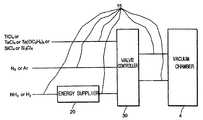
- FIG. 2is a conceptual block diagram showing an atomic layer deposition apparatus using remote plasma, according to the present invention
- FIG. 3is a flow diagram corresponding to a reactive gas feeder for use in an atomic layer deposition apparatus using remote plasma in accordance with an embodiment of the present invention.
- FIGS. 4A and 4Bshow the operation of the apparatus of the present invention in terms of the operational (open/close) states of the controllers according to the time sequence for supplying reaction materials stepwise.
- the conventional atomic layer deposition apparatuscomprises a feeder 1 for feeding a plurality of reactive gases alternately, a susceptor 3 for receiving wafers 2 , and a chamber 4 for housing the susceptor 3 , where the reactive gases fed from the carrier 1 are deposited onto the wafers 2 .
- the reactive gas feedercomprises a plurality of transfer pipes 15 for guiding a first reactive gas (NH 3 or H 2 ), a second reactive gas (TiCl 4 , TaCl 5 , SiCl 4 , Si 2 Cl 6 ), and a carrier gas for carrying the reactive gases, into a vacuum chamber 4 ; an energy supplier 20 , provided inside the transfer pipes 15 , for supplying excitation energy to generate excited plasma to ionize the first reactive gas; and a valve controller 30 , established in the transfer pipes 15 , for alternately feeding into a vacuum chamber 4 the second reactive gas and the first reactive gas ionized by the plasma excited in the energy supplier 20 .
- the reactive materialsare deposited on semiconductor wafers.
- the energy supplier 20is a plasma generator where the first reactive gas is ionized by excited plasma using a high frequency
- valve controller 30is operated to feed the carrier gas to purge the reactive gas atmosphere at each process after the feeding of the first and second gases.
- the reactive gas feedercomprises a flow controller 6 for controlling a solid source of the reactive material TaCl 5 and the reactive gas generated from the solid source in predetermined quantities, and a first feeding valve unit 23 (V 1 , V 2 , V 3 , V 9 , V 11 ) for transferring the reactive gas generated with the passage of time to a vacuum chamber or bypass line P.
- the reactive gas feedercomprises a purge valve unit 27 (V 4 , V 5 , V 13 ) for supplying inert gas (N 2 and Ar) to purge the initially introduced reactive gas out of the vacuum chamber.
- a mass flow controller MFC 1for controlling the flow of carrier gas at a constant amount.
- a mass flow controller MFC 2is provided for supplying NH 3 or H 2 gas sources at a constant flow rate.
- the reactive gas feederfurther comprises a plasma generator 7 for exciting the gas sources to ionization with a high frequency of 13.56 MHz to generate plasma and a second feeding unit 25 (V 6 , V 7 , V 8 , V 10 ) for transferring the gas ionized by the plasma of NH 3 through the vacuum chamber or the bypass line P sequentially with time.
- the first feeding valve unit 23(V 1 , V 2 , V 3 , V 9 , V 11 ), the second feeding valve unit 25 (V 9 , V 7 , V 8 , V 10 ), and the purge valve unit 27 (V 4 , V 5 , V 13 ), collectively named a valve operating unit 21 , function, in concert, to feed the gas ionized by the plasma of the plasma generator 7 and the reactive gas of the reactive gas generator alternately into the chamber and to supply a cleaning gas subsequent to the feeding of any of the reactive gases.
- the first feeding valve unit 23(V 1 , V 2 , V 3 , V 9 , V 11 ), the second feeding valve unit 25 (V 6 , V 7 , V 8 , V 10 ), and the purge valve unit 27 (V 5 , V 5 , V 13 ) are under the control of a valve controller (not shown).
- the first feeding unit 23is regulated by the valve controller so as to feed the reactive gas of TaCl 5 into the vacuum chamber 4 which is then purged with inert gas such as N 2 or Ar according to the operation of the purge valve unit 27 under the control of the valve controller.
- valve controllerregulates the second feeding valve unit 25 and the purge valve unit 27 in such a way that the gas ionized by the plasma of NH 3 or H 2 is fed into the vacuum chamber 4 which is then purged with inert gas containing N 2 or Ar.
- the gas used to purge the vacuum chamberis a carrier gas.
- the first feeding valve unit 23(V 1 , V 2 , V 9 , V 11 ), the second feeding valve unit 25 (V 6 , V 7 , V 8 , V 10 ), and the purge valve unit 27 (V 4 , V 5 , V 13 ) are operated under the control of the valve controller so as to implement a cycle consisting of the feeding of the reactive gas of TaCl 5 , the purging with inert gas, the feeding of a gas ionized by plasma of NH 3 or H 2 , and the purging with inert gas, in sequence.
- the cyclemay be performed repeatedly according to designed processes.
- the carrier gasmay be supplied, along with the reactive gas of TaCl 5 or the gas ionized with plasma of NH 3 or H 2 , in order to quickly carry the reaction materials.
- the reactive gas feedercomprises a container 8 for storing a reaction material by use of pressurized gas, an abstracter 9 for removing the pressurized gas from a pressurized liquid material to carry a pure reactive liquid only, a liquid flow controller 10 for supplying a predetermined amount of the liquid reactive gas source, and an evaporizer 11 for evaporating the carried liquid at a predetermined temperature.
- the reactive gas induced from the evaporizer 11is passed through the first feeding valve unit 23 (V 1 , V 2 , V 3 , V 9 , V 11 ) into the vacuum chamber or bypass line and thus takes part in the operation cycle in concert with the plasma-ionized gas and the purging gas which are regulated by the second feeding valve unit 25 and the purge valve unit 27 , respectively.
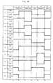
- FIG. 4there is illustrated the atomic layer using remote plasma in terms of the operational (open/close) states of the controllers V 1 to V 10 according to the time sequence for supplying reaction materials stepwise.
- Steps 1 to 6show a process flow according to time sequence. Preliminary operation steps, represented by Steps 1 and 2 , are set to quickly implement the initial process after the introduction of wafers into the reactor. In Steps 3 to 6 , which constitute a continuously repeated cycle, 1 feeding/1 purge and 1 feeding/2 purges are carried out with the first reactive gas, the second reactive gas and the cleaning gas at each step according to time sequence.
- FIG. 4 ashows the process flow of atomic layer deposition with remote plasma generation being in ON/OFF states, in which the generated remote plasma is introduced into the vacuum chamber and the bypass.
- the second reactive gas and the carrier gasare needed.
- the valves V 1 and V 3are opened under the closed state of the first feeding valve unit 23 (V 1 , V 2 , V 3 , V 9 , V 11 ) to provide the second reactive gas while only the valve V 5 is opened in the purge valve unit 27 (V 4 , V 5 and V 13 ) with the other valves closed for provision of the carrier gas.
- the purge A with inert gas containing N 2 and Arit can be carried out by opening the valve V 4 out of the purge valve unit (V 4 , V 5 , V 13 ) to clean the feeding pipe connected to the valve V 3 .
- valves V 2 and V 9are opened (bypass) to maintain the feeding pressure constant while the valves V 6 and V 8 are opened (bypass) to control the pressure for the second feeding.
- V 13 of the purge unitis open with V 5 remaining closed.
- the feeding (B) of the first reactive gas ionized by the plasma of NH 3 or H 2 into the vacuum chamberis performed with the aid of the carrier gas.
- the valves V 6 and V 7are opened under the closed state of the second feeding valve unit 25 (V 6 , V 7 , V 8 , V 10 ) to provide the gas ionized by plasma, while only the valve V 4 is opened in the purge valve unit 27 (V 4 , V 5 and V 13 ) with the other valves closed for provision of the carrier gas.
- valves V 2 and V 9are opened (bypass) to maintain the feeding pressure constant.
- valve V 5 out of the purge valve unit(V 4 , V 5 , V 13 ) is opened to clean the feeding pipe connected to the valve V 7 .
- pressure control upon feeding of reactive gasesit is achieved by opening the valves V 1 and V 2 for the first feeding and the valves V 8 and V 10 for the second feeding.
- valve controlis conducted in such a way as to maintain the pressure of the energy supplier constant.
- various thin filmsTi, TiN, Ta, TaN, SiN
- the thin film to be depositedcan be desirably adjusted in thickness. After one cycle of the process, the thin film is formed at ones of Angstrom.
- the deposition of Ti, TiN, Ta, TaN and SiN thin filmsis performed by use of reactive gases comprising NH 3 or H 2 , and any one of a solid source of TaCl 5 and a liquid source of TiCl 4 , Ta(OC 2 H 5 ) 5 , SiCl 4 or Si 2 Cl 6 , in combination with an inert gas in accordance with the time sequence suggested in FIGS. 4 a and 4 b.
- reactive materials for use in the formation of oxide, nitride and metal thin films through atomic layer depositioncan be supplied at low temperatures, instead of by use of high heat energy, in the process and apparatus using remote plasma of the present invention, thereby yielding thin films almost free of impurities.
- the use of the excited reactive gasrestrains the formation of impurities in addition to allowing the formation of thin films at low temperatures, thereby improving the production yield.
Landscapes
- Chemical & Material Sciences (AREA)
- Engineering & Computer Science (AREA)
- Mechanical Engineering (AREA)
- Chemical Kinetics & Catalysis (AREA)
- General Chemical & Material Sciences (AREA)
- Materials Engineering (AREA)
- Metallurgy (AREA)
- Organic Chemistry (AREA)
- Inorganic Chemistry (AREA)
- Physics & Mathematics (AREA)
- Electromagnetism (AREA)
- Plasma & Fusion (AREA)
- Chemical Vapour Deposition (AREA)
Abstract
Description
Claims (15)
Priority Applications (1)
| Application Number | Priority Date | Filing Date | Title |
|---|---|---|---|
| US09/973,760US6656282B2 (en) | 2001-10-11 | 2001-10-11 | Atomic layer deposition apparatus and process using remote plasma |
Applications Claiming Priority (1)
| Application Number | Priority Date | Filing Date | Title |
|---|---|---|---|
| US09/973,760US6656282B2 (en) | 2001-10-11 | 2001-10-11 | Atomic layer deposition apparatus and process using remote plasma |
Publications (2)
| Publication Number | Publication Date |
|---|---|
| US20030070617A1 US20030070617A1 (en) | 2003-04-17 |
| US6656282B2true US6656282B2 (en) | 2003-12-02 |
Family
ID=25521197
Family Applications (1)
| Application Number | Title | Priority Date | Filing Date |
|---|---|---|---|
| US09/973,760Expired - LifetimeUS6656282B2 (en) | 2001-10-11 | 2001-10-11 | Atomic layer deposition apparatus and process using remote plasma |
Country Status (1)
| Country | Link |
|---|---|
| US (1) | US6656282B2 (en) |
Cited By (313)
| Publication number | Priority date | Publication date | Assignee | Title |
|---|---|---|---|---|
| US20040140513A1 (en)* | 2002-08-22 | 2004-07-22 | Micron Technology, Inc. | Atomic layer deposition of CMOS gates with variable work functions |
| US20050048785A1 (en)* | 2003-08-26 | 2005-03-03 | Lam Research Corporation | Reduction of feature critical dimensions |
| US20050120954A1 (en)* | 2002-05-24 | 2005-06-09 | Carpenter Craig M. | Apparatus for controlling gas pulsing in processes for depositing materials onto micro-device workpieces |
| US20050193947A1 (en)* | 2002-08-15 | 2005-09-08 | Cem Basceri | Deposition reactors and systems |
| US20050223982A1 (en)* | 2002-04-19 | 2005-10-13 | Park Young H | Apparatus and method for depositing thin film on wafer using remote plasma |
| US6967154B2 (en)* | 2002-08-26 | 2005-11-22 | Micron Technology, Inc. | Enhanced atomic layer deposition |
| US20050287806A1 (en)* | 2004-06-24 | 2005-12-29 | Hiroyuki Matsuura | Vertical CVD apparatus and CVD method using the same |
| US20060063346A1 (en)* | 2004-06-10 | 2006-03-23 | Jong-Cheol Lee | Method of forming a layer and method of forming a capacitor of a semiconductor device having the same |
| US20060060139A1 (en)* | 2004-04-12 | 2006-03-23 | Mks Instruments, Inc. | Precursor gas delivery with carrier gas mixing |
| US20060134917A1 (en)* | 2004-12-16 | 2006-06-22 | Lam Research Corporation | Reduction of etch mask feature critical dimensions |
| US20060194439A1 (en)* | 2005-03-08 | 2006-08-31 | Lam Research Corporation | Etch with striation control |
| US20060205220A1 (en)* | 2005-03-08 | 2006-09-14 | Lam Research Corporation | Stabilized photoresist structure for etching process |
| US20060210723A1 (en)* | 2005-03-21 | 2006-09-21 | Tokyo Electron Limited | Plasma enhanced atomic layer deposition system and method |
| US20070042607A1 (en)* | 2005-08-18 | 2007-02-22 | Lam Research Corporation | Etch features with reduced line edge roughness |
| WO2007061273A1 (en)* | 2005-11-28 | 2007-05-31 | Aet Co., Ltd. | Method of forming silicon film by two step deposition |
| US7279398B2 (en) | 2003-09-17 | 2007-10-09 | Micron Technology, Inc. | Microfeature workpiece processing apparatus and methods for controlling deposition of materials on microfeature workpieces |
| US7282239B2 (en) | 2003-09-18 | 2007-10-16 | Micron Technology, Inc. | Systems and methods for depositing material onto microfeature workpieces in reaction chambers |
| US7309646B1 (en) | 2006-10-10 | 2007-12-18 | Lam Research Corporation | De-fluoridation process |
| US7335396B2 (en) | 2003-04-24 | 2008-02-26 | Micron Technology, Inc. | Methods for controlling mass flow rates and pressures in passageways coupled to reaction chambers and systems for depositing material onto microfeature workpieces in reaction chambers |
| KR100819336B1 (en) | 2004-02-19 | 2008-04-02 | 한국과학기술원 | Plasma generating method and apparatus thereof having low electron temperature |
| US7393562B2 (en)* | 2002-02-25 | 2008-07-01 | Micron Technology, Inc. | Deposition methods for improved delivery of metastable species |
| US20080160214A1 (en)* | 2002-10-08 | 2008-07-03 | Masanori Sakai | Substrate processing apparatus |
| US7422635B2 (en) | 2003-08-28 | 2008-09-09 | Micron Technology, Inc. | Methods and apparatus for processing microfeature workpieces, e.g., for depositing materials on microfeature workpieces |
| US7581511B2 (en) | 2003-10-10 | 2009-09-01 | Micron Technology, Inc. | Apparatus and methods for manufacturing microfeatures on workpieces using plasma vapor processes |
| US20090223448A1 (en)* | 2008-01-31 | 2009-09-10 | Hitachi Kokusai Electric Inc. | Substrate processing apparatus and method for manufacturing semiconductor device |
| US7588804B2 (en) | 2002-08-15 | 2009-09-15 | Micron Technology, Inc. | Reactors with isolated gas connectors and methods for depositing materials onto micro-device workpieces |
| US7629256B2 (en) | 2007-05-14 | 2009-12-08 | Asm International N.V. | In situ silicon and titanium nitride deposition |
| US7691757B2 (en) | 2006-06-22 | 2010-04-06 | Asm International N.V. | Deposition of complex nitride films |
| US7692222B2 (en) | 2006-11-07 | 2010-04-06 | Raytheon Company | Atomic layer deposition in the formation of gate structures for III-V semiconductor |
| US7699932B2 (en) | 2004-06-02 | 2010-04-20 | Micron Technology, Inc. | Reactors, systems and methods for depositing thin films onto microfeature workpieces |
| US7709402B2 (en) | 2006-02-16 | 2010-05-04 | Micron Technology, Inc. | Conductive layers for hafnium silicon oxynitride films |
| US7732350B2 (en) | 2004-09-22 | 2010-06-08 | Asm International N.V. | Chemical vapor deposition of TiN films in a batch reactor |
| US20100140077A1 (en)* | 2008-12-04 | 2010-06-10 | Bon-Woong Koo | Excited gas injection for ion implant control |
| US7771537B2 (en) | 2003-12-10 | 2010-08-10 | Micron Technology, Inc. | Methods and systems for controlling temperature during microfeature workpiece processing, E.G. CVD deposition |
| US7833906B2 (en) | 2008-12-11 | 2010-11-16 | Asm International N.V. | Titanium silicon nitride deposition |
| US8384192B2 (en) | 2004-01-28 | 2013-02-26 | Micron Technology, Inc. | Methods for forming small-scale capacitor structures |
| US8633110B2 (en) | 2005-07-20 | 2014-01-21 | Micron Technology, Inc. | Titanium nitride films |
| US20140216339A1 (en)* | 2011-08-01 | 2014-08-07 | Fujikin Incorporated | Raw material vaporizing and supplying apparatus |
| US9632511B2 (en) | 2011-05-10 | 2017-04-25 | Fujikin Incorporated | Pressure type flow control system with flow monitoring, and method for detecting anomaly in fluid supply system and handling method at abnormal monitoring flow rate using the same |
| US9631777B2 (en) | 2011-09-06 | 2017-04-25 | Fujikin Incorporated | Raw material vaporizing and supplying apparatus equipped with raw material concentration |
| US11001925B2 (en) | 2016-12-19 | 2021-05-11 | Asm Ip Holding B.V. | Substrate processing apparatus |
| US11004977B2 (en) | 2017-07-19 | 2021-05-11 | Asm Ip Holding B.V. | Method for depositing a group IV semiconductor and related semiconductor device structures |
| US11018002B2 (en) | 2017-07-19 | 2021-05-25 | Asm Ip Holding B.V. | Method for selectively depositing a Group IV semiconductor and related semiconductor device structures |
| US11015245B2 (en) | 2014-03-19 | 2021-05-25 | Asm Ip Holding B.V. | Gas-phase reactor and system having exhaust plenum and components thereof |
| US11022879B2 (en) | 2017-11-24 | 2021-06-01 | Asm Ip Holding B.V. | Method of forming an enhanced unexposed photoresist layer |
| US11031242B2 (en) | 2018-11-07 | 2021-06-08 | Asm Ip Holding B.V. | Methods for depositing a boron doped silicon germanium film |
| USD922229S1 (en) | 2019-06-05 | 2021-06-15 | Asm Ip Holding B.V. | Device for controlling a temperature of a gas supply unit |
| US11049751B2 (en) | 2018-09-14 | 2021-06-29 | Asm Ip Holding B.V. | Cassette supply system to store and handle cassettes and processing apparatus equipped therewith |
| US11056344B2 (en) | 2017-08-30 | 2021-07-06 | Asm Ip Holding B.V. | Layer forming method |
| US11053591B2 (en) | 2018-08-06 | 2021-07-06 | Asm Ip Holding B.V. | Multi-port gas injection system and reactor system including same |
| US11069510B2 (en) | 2017-08-30 | 2021-07-20 | Asm Ip Holding B.V. | Substrate processing apparatus |
| US11081345B2 (en) | 2018-02-06 | 2021-08-03 | Asm Ip Holding B.V. | Method of post-deposition treatment for silicon oxide film |
| US11088002B2 (en) | 2018-03-29 | 2021-08-10 | Asm Ip Holding B.V. | Substrate rack and a substrate processing system and method |
| US11087997B2 (en) | 2018-10-31 | 2021-08-10 | Asm Ip Holding B.V. | Substrate processing apparatus for processing substrates |
| US11094546B2 (en) | 2017-10-05 | 2021-08-17 | Asm Ip Holding B.V. | Method for selectively depositing a metallic film on a substrate |
| US11094582B2 (en) | 2016-07-08 | 2021-08-17 | Asm Ip Holding B.V. | Selective deposition method to form air gaps |
| US11101370B2 (en) | 2016-05-02 | 2021-08-24 | Asm Ip Holding B.V. | Method of forming a germanium oxynitride film |
| US11107676B2 (en) | 2016-07-28 | 2021-08-31 | Asm Ip Holding B.V. | Method and apparatus for filling a gap |
| US11114294B2 (en) | 2019-03-08 | 2021-09-07 | Asm Ip Holding B.V. | Structure including SiOC layer and method of forming same |
| US11114283B2 (en) | 2018-03-16 | 2021-09-07 | Asm Ip Holding B.V. | Reactor, system including the reactor, and methods of manufacturing and using same |
| USD930782S1 (en) | 2019-08-22 | 2021-09-14 | Asm Ip Holding B.V. | Gas distributor |
| US11127589B2 (en) | 2019-02-01 | 2021-09-21 | Asm Ip Holding B.V. | Method of topology-selective film formation of silicon oxide |
| US11127617B2 (en) | 2017-11-27 | 2021-09-21 | Asm Ip Holding B.V. | Storage device for storing wafer cassettes for use with a batch furnace |
| USD931978S1 (en) | 2019-06-27 | 2021-09-28 | Asm Ip Holding B.V. | Showerhead vacuum transport |
| US11139308B2 (en) | 2015-12-29 | 2021-10-05 | Asm Ip Holding B.V. | Atomic layer deposition of III-V compounds to form V-NAND devices |
| US11139191B2 (en) | 2017-08-09 | 2021-10-05 | Asm Ip Holding B.V. | Storage apparatus for storing cassettes for substrates and processing apparatus equipped therewith |
| US11158513B2 (en) | 2018-12-13 | 2021-10-26 | Asm Ip Holding B.V. | Methods for forming a rhenium-containing film on a substrate by a cyclical deposition process and related semiconductor device structures |
| US11164955B2 (en) | 2017-07-18 | 2021-11-02 | Asm Ip Holding B.V. | Methods for forming a semiconductor device structure and related semiconductor device structures |
| US11171025B2 (en) | 2019-01-22 | 2021-11-09 | Asm Ip Holding B.V. | Substrate processing device |
| USD935572S1 (en) | 2019-05-24 | 2021-11-09 | Asm Ip Holding B.V. | Gas channel plate |
| US11168395B2 (en) | 2018-06-29 | 2021-11-09 | Asm Ip Holding B.V. | Temperature-controlled flange and reactor system including same |
| US11205585B2 (en) | 2016-07-28 | 2021-12-21 | Asm Ip Holding B.V. | Substrate processing apparatus and method of operating the same |
| US11217444B2 (en) | 2018-11-30 | 2022-01-04 | Asm Ip Holding B.V. | Method for forming an ultraviolet radiation responsive metal oxide-containing film |
| USD940837S1 (en) | 2019-08-22 | 2022-01-11 | Asm Ip Holding B.V. | Electrode |
| US11222772B2 (en) | 2016-12-14 | 2022-01-11 | Asm Ip Holding B.V. | Substrate processing apparatus |
| US11227789B2 (en) | 2019-02-20 | 2022-01-18 | Asm Ip Holding B.V. | Method and apparatus for filling a recess formed within a substrate surface |
| US11227782B2 (en) | 2019-07-31 | 2022-01-18 | Asm Ip Holding B.V. | Vertical batch furnace assembly |
| US11232963B2 (en) | 2018-10-03 | 2022-01-25 | Asm Ip Holding B.V. | Substrate processing apparatus and method |
| US11230766B2 (en) | 2018-03-29 | 2022-01-25 | Asm Ip Holding B.V. | Substrate processing apparatus and method |
| US11233133B2 (en) | 2015-10-21 | 2022-01-25 | Asm Ip Holding B.V. | NbMC layers |
| US11242598B2 (en) | 2015-06-26 | 2022-02-08 | Asm Ip Holding B.V. | Structures including metal carbide material, devices including the structures, and methods of forming same |
| US11244825B2 (en) | 2018-11-16 | 2022-02-08 | Asm Ip Holding B.V. | Methods for depositing a transition metal chalcogenide film on a substrate by a cyclical deposition process |
| US11251040B2 (en) | 2019-02-20 | 2022-02-15 | Asm Ip Holding B.V. | Cyclical deposition method including treatment step and apparatus for same |
| US11251035B2 (en) | 2016-12-22 | 2022-02-15 | Asm Ip Holding B.V. | Method of forming a structure on a substrate |
| US11251068B2 (en) | 2018-10-19 | 2022-02-15 | Asm Ip Holding B.V. | Substrate processing apparatus and substrate processing method |
| USD944946S1 (en) | 2019-06-14 | 2022-03-01 | Asm Ip Holding B.V. | Shower plate |
| US11270899B2 (en) | 2018-06-04 | 2022-03-08 | Asm Ip Holding B.V. | Wafer handling chamber with moisture reduction |
| US11274369B2 (en) | 2018-09-11 | 2022-03-15 | Asm Ip Holding B.V. | Thin film deposition method |
| US11282698B2 (en) | 2019-07-19 | 2022-03-22 | Asm Ip Holding B.V. | Method of forming topology-controlled amorphous carbon polymer film |
| US11286558B2 (en) | 2019-08-23 | 2022-03-29 | Asm Ip Holding B.V. | Methods for depositing a molybdenum nitride film on a surface of a substrate by a cyclical deposition process and related semiconductor device structures including a molybdenum nitride film |
| US11289326B2 (en) | 2019-05-07 | 2022-03-29 | Asm Ip Holding B.V. | Method for reforming amorphous carbon polymer film |
| US11286562B2 (en) | 2018-06-08 | 2022-03-29 | Asm Ip Holding B.V. | Gas-phase chemical reactor and method of using same |
| US11295980B2 (en) | 2017-08-30 | 2022-04-05 | Asm Ip Holding B.V. | Methods for depositing a molybdenum metal film over a dielectric surface of a substrate by a cyclical deposition process and related semiconductor device structures |
| USD947913S1 (en) | 2019-05-17 | 2022-04-05 | Asm Ip Holding B.V. | Susceptor shaft |
| US11296189B2 (en) | 2018-06-21 | 2022-04-05 | Asm Ip Holding B.V. | Method for depositing a phosphorus doped silicon arsenide film and related semiconductor device structures |
| USD948463S1 (en) | 2018-10-24 | 2022-04-12 | Asm Ip Holding B.V. | Susceptor for semiconductor substrate supporting apparatus |
| US11306395B2 (en) | 2017-06-28 | 2022-04-19 | Asm Ip Holding B.V. | Methods for depositing a transition metal nitride film on a substrate by atomic layer deposition and related deposition apparatus |
| USD949319S1 (en) | 2019-08-22 | 2022-04-19 | Asm Ip Holding B.V. | Exhaust duct |
| US11315794B2 (en) | 2019-10-21 | 2022-04-26 | Asm Ip Holding B.V. | Apparatus and methods for selectively etching films |
| US11342216B2 (en) | 2019-02-20 | 2022-05-24 | Asm Ip Holding B.V. | Cyclical deposition method and apparatus for filling a recess formed within a substrate surface |
| US11339476B2 (en) | 2019-10-08 | 2022-05-24 | Asm Ip Holding B.V. | Substrate processing device having connection plates, substrate processing method |
| US11345999B2 (en) | 2019-06-06 | 2022-05-31 | Asm Ip Holding B.V. | Method of using a gas-phase reactor system including analyzing exhausted gas |
| US11355338B2 (en) | 2019-05-10 | 2022-06-07 | Asm Ip Holding B.V. | Method of depositing material onto a surface and structure formed according to the method |
| US11361990B2 (en) | 2018-05-28 | 2022-06-14 | Asm Ip Holding B.V. | Substrate processing method and device manufactured by using the same |
| US11374112B2 (en) | 2017-07-19 | 2022-06-28 | Asm Ip Holding B.V. | Method for depositing a group IV semiconductor and related semiconductor device structures |
| US11378337B2 (en) | 2019-03-28 | 2022-07-05 | Asm Ip Holding B.V. | Door opener and substrate processing apparatus provided therewith |
| US11387106B2 (en) | 2018-02-14 | 2022-07-12 | Asm Ip Holding B.V. | Method for depositing a ruthenium-containing film on a substrate by a cyclical deposition process |
| US11387120B2 (en) | 2017-09-28 | 2022-07-12 | Asm Ip Holding B.V. | Chemical dispensing apparatus and methods for dispensing a chemical to a reaction chamber |
| US11393690B2 (en) | 2018-01-19 | 2022-07-19 | Asm Ip Holding B.V. | Deposition method |
| US11390945B2 (en) | 2019-07-03 | 2022-07-19 | Asm Ip Holding B.V. | Temperature control assembly for substrate processing apparatus and method of using same |
| US11390950B2 (en) | 2017-01-10 | 2022-07-19 | Asm Ip Holding B.V. | Reactor system and method to reduce residue buildup during a film deposition process |
| US11390946B2 (en) | 2019-01-17 | 2022-07-19 | Asm Ip Holding B.V. | Methods of forming a transition metal containing film on a substrate by a cyclical deposition process |
| US11396702B2 (en) | 2016-11-15 | 2022-07-26 | Asm Ip Holding B.V. | Gas supply unit and substrate processing apparatus including the gas supply unit |
| US11398382B2 (en) | 2018-03-27 | 2022-07-26 | Asm Ip Holding B.V. | Method of forming an electrode on a substrate and a semiconductor device structure including an electrode |
| US11401605B2 (en) | 2019-11-26 | 2022-08-02 | Asm Ip Holding B.V. | Substrate processing apparatus |
| US11411088B2 (en) | 2018-11-16 | 2022-08-09 | Asm Ip Holding B.V. | Methods for forming a metal silicate film on a substrate in a reaction chamber and related semiconductor device structures |
| US11410851B2 (en) | 2017-02-15 | 2022-08-09 | Asm Ip Holding B.V. | Methods for forming a metallic film on a substrate by cyclical deposition and related semiconductor device structures |
| US11414760B2 (en) | 2018-10-08 | 2022-08-16 | Asm Ip Holding B.V. | Substrate support unit, thin film deposition apparatus including the same, and substrate processing apparatus including the same |
| US11417545B2 (en) | 2017-08-08 | 2022-08-16 | Asm Ip Holding B.V. | Radiation shield |
| US11424119B2 (en) | 2019-03-08 | 2022-08-23 | Asm Ip Holding B.V. | Method for selective deposition of silicon nitride layer and structure including selectively-deposited silicon nitride layer |
| US11430640B2 (en) | 2019-07-30 | 2022-08-30 | Asm Ip Holding B.V. | Substrate processing apparatus |
| US11430674B2 (en) | 2018-08-22 | 2022-08-30 | Asm Ip Holding B.V. | Sensor array, apparatus for dispensing a vapor phase reactant to a reaction chamber and related methods |
| US11437241B2 (en) | 2020-04-08 | 2022-09-06 | Asm Ip Holding B.V. | Apparatus and methods for selectively etching silicon oxide films |
| US11443926B2 (en) | 2019-07-30 | 2022-09-13 | Asm Ip Holding B.V. | Substrate processing apparatus |
| US11447864B2 (en) | 2019-04-19 | 2022-09-20 | Asm Ip Holding B.V. | Layer forming method and apparatus |
| US11447861B2 (en) | 2016-12-15 | 2022-09-20 | Asm Ip Holding B.V. | Sequential infiltration synthesis apparatus and a method of forming a patterned structure |
| US11453943B2 (en) | 2016-05-25 | 2022-09-27 | Asm Ip Holding B.V. | Method for forming carbon-containing silicon/metal oxide or nitride film by ALD using silicon precursor and hydrocarbon precursor |
| USD965044S1 (en) | 2019-08-19 | 2022-09-27 | Asm Ip Holding B.V. | Susceptor shaft |
| USD965524S1 (en) | 2019-08-19 | 2022-10-04 | Asm Ip Holding B.V. | Susceptor support |
| US11469098B2 (en) | 2018-05-08 | 2022-10-11 | Asm Ip Holding B.V. | Methods for depositing an oxide film on a substrate by a cyclical deposition process and related device structures |
| US11476109B2 (en) | 2019-06-11 | 2022-10-18 | Asm Ip Holding B.V. | Method of forming an electronic structure using reforming gas, system for performing the method, and structure formed using the method |
| US11473195B2 (en) | 2018-03-01 | 2022-10-18 | Asm Ip Holding B.V. | Semiconductor processing apparatus and a method for processing a substrate |
| US11482533B2 (en) | 2019-02-20 | 2022-10-25 | Asm Ip Holding B.V. | Apparatus and methods for plug fill deposition in 3-D NAND applications |
| US11482418B2 (en) | 2018-02-20 | 2022-10-25 | Asm Ip Holding B.V. | Substrate processing method and apparatus |
| US11482412B2 (en) | 2018-01-19 | 2022-10-25 | Asm Ip Holding B.V. | Method for depositing a gap-fill layer by plasma-assisted deposition |
| US11488854B2 (en) | 2020-03-11 | 2022-11-01 | Asm Ip Holding B.V. | Substrate handling device with adjustable joints |
| US11488819B2 (en) | 2018-12-04 | 2022-11-01 | Asm Ip Holding B.V. | Method of cleaning substrate processing apparatus |
| US11495459B2 (en) | 2019-09-04 | 2022-11-08 | Asm Ip Holding B.V. | Methods for selective deposition using a sacrificial capping layer |
| US11492703B2 (en) | 2018-06-27 | 2022-11-08 | Asm Ip Holding B.V. | Cyclic deposition methods for forming metal-containing material and films and structures including the metal-containing material |
| US11501956B2 (en) | 2012-10-12 | 2022-11-15 | Asm Ip Holding B.V. | Semiconductor reaction chamber showerhead |
| US11499222B2 (en) | 2018-06-27 | 2022-11-15 | Asm Ip Holding B.V. | Cyclic deposition methods for forming metal-containing material and films and structures including the metal-containing material |
| US11501968B2 (en) | 2019-11-15 | 2022-11-15 | Asm Ip Holding B.V. | Method for providing a semiconductor device with silicon filled gaps |
| US11499226B2 (en) | 2018-11-02 | 2022-11-15 | Asm Ip Holding B.V. | Substrate supporting unit and a substrate processing device including the same |
| US11501973B2 (en) | 2018-01-16 | 2022-11-15 | Asm Ip Holding B.V. | Method for depositing a material film on a substrate within a reaction chamber by a cyclical deposition process and related device structures |
| US11515187B2 (en) | 2020-05-01 | 2022-11-29 | Asm Ip Holding B.V. | Fast FOUP swapping with a FOUP handler |
| US11515188B2 (en) | 2019-05-16 | 2022-11-29 | Asm Ip Holding B.V. | Wafer boat handling device, vertical batch furnace and method |
| US11521851B2 (en) | 2020-02-03 | 2022-12-06 | Asm Ip Holding B.V. | Method of forming structures including a vanadium or indium layer |
| US11527403B2 (en) | 2019-12-19 | 2022-12-13 | Asm Ip Holding B.V. | Methods for filling a gap feature on a substrate surface and related semiconductor structures |
| US11527400B2 (en) | 2019-08-23 | 2022-12-13 | Asm Ip Holding B.V. | Method for depositing silicon oxide film having improved quality by peald using bis(diethylamino)silane |
| US11530876B2 (en) | 2020-04-24 | 2022-12-20 | Asm Ip Holding B.V. | Vertical batch furnace assembly comprising a cooling gas supply |
| US11530483B2 (en) | 2018-06-21 | 2022-12-20 | Asm Ip Holding B.V. | Substrate processing system |
| US11532757B2 (en) | 2016-10-27 | 2022-12-20 | Asm Ip Holding B.V. | Deposition of charge trapping layers |
| US11551912B2 (en) | 2020-01-20 | 2023-01-10 | Asm Ip Holding B.V. | Method of forming thin film and method of modifying surface of thin film |
| US11551925B2 (en) | 2019-04-01 | 2023-01-10 | Asm Ip Holding B.V. | Method for manufacturing a semiconductor device |
| US11557474B2 (en) | 2019-07-29 | 2023-01-17 | Asm Ip Holding B.V. | Methods for selective deposition utilizing n-type dopants and/or alternative dopants to achieve high dopant incorporation |
| USD975665S1 (en) | 2019-05-17 | 2023-01-17 | Asm Ip Holding B.V. | Susceptor shaft |
| US11562901B2 (en) | 2019-09-25 | 2023-01-24 | Asm Ip Holding B.V. | Substrate processing method |
| US11572620B2 (en) | 2018-11-06 | 2023-02-07 | Asm Ip Holding B.V. | Methods for selectively depositing an amorphous silicon film on a substrate |
| US11581186B2 (en) | 2016-12-15 | 2023-02-14 | Asm Ip Holding B.V. | Sequential infiltration synthesis apparatus |
| US11587814B2 (en) | 2019-07-31 | 2023-02-21 | Asm Ip Holding B.V. | Vertical batch furnace assembly |
| US11587815B2 (en) | 2019-07-31 | 2023-02-21 | Asm Ip Holding B.V. | Vertical batch furnace assembly |
| US11587821B2 (en) | 2017-08-08 | 2023-02-21 | Asm Ip Holding B.V. | Substrate lift mechanism and reactor including same |
| US11594600B2 (en) | 2019-11-05 | 2023-02-28 | Asm Ip Holding B.V. | Structures with doped semiconductor layers and methods and systems for forming same |
| USD979506S1 (en) | 2019-08-22 | 2023-02-28 | Asm Ip Holding B.V. | Insulator |
| US11594450B2 (en) | 2019-08-22 | 2023-02-28 | Asm Ip Holding B.V. | Method for forming a structure with a hole |
| USD980814S1 (en) | 2021-05-11 | 2023-03-14 | Asm Ip Holding B.V. | Gas distributor for substrate processing apparatus |
| US11605528B2 (en) | 2019-07-09 | 2023-03-14 | Asm Ip Holding B.V. | Plasma device using coaxial waveguide, and substrate treatment method |
| USD980813S1 (en) | 2021-05-11 | 2023-03-14 | Asm Ip Holding B.V. | Gas flow control plate for substrate processing apparatus |
| US11610774B2 (en) | 2019-10-02 | 2023-03-21 | Asm Ip Holding B.V. | Methods for forming a topographically selective silicon oxide film by a cyclical plasma-enhanced deposition process |
| US11610775B2 (en) | 2016-07-28 | 2023-03-21 | Asm Ip Holding B.V. | Method and apparatus for filling a gap |
| USD981973S1 (en) | 2021-05-11 | 2023-03-28 | Asm Ip Holding B.V. | Reactor wall for substrate processing apparatus |
| US11615970B2 (en) | 2019-07-17 | 2023-03-28 | Asm Ip Holding B.V. | Radical assist ignition plasma system and method |
| US11626308B2 (en) | 2020-05-13 | 2023-04-11 | Asm Ip Holding B.V. | Laser alignment fixture for a reactor system |
| US11626316B2 (en) | 2019-11-20 | 2023-04-11 | Asm Ip Holding B.V. | Method of depositing carbon-containing material on a surface of a substrate, structure formed using the method, and system for forming the structure |
| US11629407B2 (en) | 2019-02-22 | 2023-04-18 | Asm Ip Holding B.V. | Substrate processing apparatus and method for processing substrates |
| US11629406B2 (en) | 2018-03-09 | 2023-04-18 | Asm Ip Holding B.V. | Semiconductor processing apparatus comprising one or more pyrometers for measuring a temperature of a substrate during transfer of the substrate |
| US11637014B2 (en) | 2019-10-17 | 2023-04-25 | Asm Ip Holding B.V. | Methods for selective deposition of doped semiconductor material |
| US11637011B2 (en) | 2019-10-16 | 2023-04-25 | Asm Ip Holding B.V. | Method of topology-selective film formation of silicon oxide |
| US11639548B2 (en) | 2019-08-21 | 2023-05-02 | Asm Ip Holding B.V. | Film-forming material mixed-gas forming device and film forming device |
| US11639811B2 (en) | 2017-11-27 | 2023-05-02 | Asm Ip Holding B.V. | Apparatus including a clean mini environment |
| US11646204B2 (en) | 2020-06-24 | 2023-05-09 | Asm Ip Holding B.V. | Method for forming a layer provided with silicon |
| US11646205B2 (en) | 2019-10-29 | 2023-05-09 | Asm Ip Holding B.V. | Methods of selectively forming n-type doped material on a surface, systems for selectively forming n-type doped material, and structures formed using same |
| US11644758B2 (en) | 2020-07-17 | 2023-05-09 | Asm Ip Holding B.V. | Structures and methods for use in photolithography |
| US11646184B2 (en) | 2019-11-29 | 2023-05-09 | Asm Ip Holding B.V. | Substrate processing apparatus |
| US11646197B2 (en) | 2018-07-03 | 2023-05-09 | Asm Ip Holding B.V. | Method for depositing silicon-free carbon-containing film as gap-fill layer by pulse plasma-assisted deposition |
| US11643724B2 (en) | 2019-07-18 | 2023-05-09 | Asm Ip Holding B.V. | Method of forming structures using a neutral beam |
| US11649546B2 (en) | 2016-07-08 | 2023-05-16 | Asm Ip Holding B.V. | Organic reactants for atomic layer deposition |
| US11658035B2 (en) | 2020-06-30 | 2023-05-23 | Asm Ip Holding B.V. | Substrate processing method |
| US11658029B2 (en) | 2018-12-14 | 2023-05-23 | Asm Ip Holding B.V. | Method of forming a device structure using selective deposition of gallium nitride and system for same |
| US11658030B2 (en) | 2017-03-29 | 2023-05-23 | Asm Ip Holding B.V. | Method for forming doped metal oxide films on a substrate by cyclical deposition and related semiconductor device structures |
| US11664199B2 (en) | 2018-10-19 | 2023-05-30 | Asm Ip Holding B.V. | Substrate processing apparatus and substrate processing method |
| US11664245B2 (en) | 2019-07-16 | 2023-05-30 | Asm Ip Holding B.V. | Substrate processing device |
| US11664267B2 (en) | 2019-07-10 | 2023-05-30 | Asm Ip Holding B.V. | Substrate support assembly and substrate processing device including the same |
| US11676812B2 (en) | 2016-02-19 | 2023-06-13 | Asm Ip Holding B.V. | Method for forming silicon nitride film selectively on top/bottom portions |
| US11674220B2 (en) | 2020-07-20 | 2023-06-13 | Asm Ip Holding B.V. | Method for depositing molybdenum layers using an underlayer |
| US11680839B2 (en) | 2019-08-05 | 2023-06-20 | Asm Ip Holding B.V. | Liquid level sensor for a chemical source vessel |
| US11688603B2 (en) | 2019-07-17 | 2023-06-27 | Asm Ip Holding B.V. | Methods of forming silicon germanium structures |
| USD990441S1 (en) | 2021-09-07 | 2023-06-27 | Asm Ip Holding B.V. | Gas flow control plate |
| USD990534S1 (en) | 2020-09-11 | 2023-06-27 | Asm Ip Holding B.V. | Weighted lift pin |
| US11685991B2 (en) | 2018-02-14 | 2023-06-27 | Asm Ip Holding B.V. | Method for depositing a ruthenium-containing film on a substrate by a cyclical deposition process |
| US11705333B2 (en) | 2020-05-21 | 2023-07-18 | Asm Ip Holding B.V. | Structures including multiple carbon layers and methods of forming and using same |
| US11718913B2 (en) | 2018-06-04 | 2023-08-08 | Asm Ip Holding B.V. | Gas distribution system and reactor system including same |
| US11725277B2 (en) | 2011-07-20 | 2023-08-15 | Asm Ip Holding B.V. | Pressure transmitter for a semiconductor processing environment |
| US11725280B2 (en) | 2020-08-26 | 2023-08-15 | Asm Ip Holding B.V. | Method for forming metal silicon oxide and metal silicon oxynitride layers |
| US11735422B2 (en) | 2019-10-10 | 2023-08-22 | Asm Ip Holding B.V. | Method of forming a photoresist underlayer and structure including same |
| US11742189B2 (en) | 2015-03-12 | 2023-08-29 | Asm Ip Holding B.V. | Multi-zone reactor, system including the reactor, and method of using the same |
| US11742198B2 (en) | 2019-03-08 | 2023-08-29 | Asm Ip Holding B.V. | Structure including SiOCN layer and method of forming same |
| US11767589B2 (en) | 2020-05-29 | 2023-09-26 | Asm Ip Holding B.V. | Substrate processing device |
| US11769682B2 (en) | 2017-08-09 | 2023-09-26 | Asm Ip Holding B.V. | Storage apparatus for storing cassettes for substrates and processing apparatus equipped therewith |
| US11776846B2 (en) | 2020-02-07 | 2023-10-03 | Asm Ip Holding B.V. | Methods for depositing gap filling fluids and related systems and devices |
| US11781221B2 (en) | 2019-05-07 | 2023-10-10 | Asm Ip Holding B.V. | Chemical source vessel with dip tube |
| US11781243B2 (en) | 2020-02-17 | 2023-10-10 | Asm Ip Holding B.V. | Method for depositing low temperature phosphorous-doped silicon |
| US11795545B2 (en) | 2014-10-07 | 2023-10-24 | Asm Ip Holding B.V. | Multiple temperature range susceptor, assembly, reactor and system including the susceptor, and methods of using the same |
| US11804388B2 (en) | 2018-09-11 | 2023-10-31 | Asm Ip Holding B.V. | Substrate processing apparatus and method |
| US11804364B2 (en) | 2020-05-19 | 2023-10-31 | Asm Ip Holding B.V. | Substrate processing apparatus |
| US11802338B2 (en) | 2017-07-26 | 2023-10-31 | Asm Ip Holding B.V. | Chemical treatment, deposition and/or infiltration apparatus and method for using the same |
| US11810788B2 (en) | 2016-11-01 | 2023-11-07 | Asm Ip Holding B.V. | Methods for forming a transition metal niobium nitride film on a substrate by atomic layer deposition and related semiconductor device structures |
| US11814747B2 (en) | 2019-04-24 | 2023-11-14 | Asm Ip Holding B.V. | Gas-phase reactor system-with a reaction chamber, a solid precursor source vessel, a gas distribution system, and a flange assembly |
| US11821078B2 (en) | 2020-04-15 | 2023-11-21 | Asm Ip Holding B.V. | Method for forming precoat film and method for forming silicon-containing film |
| US11823866B2 (en) | 2020-04-02 | 2023-11-21 | Asm Ip Holding B.V. | Thin film forming method |
| US11823876B2 (en) | 2019-09-05 | 2023-11-21 | Asm Ip Holding B.V. | Substrate processing apparatus |
| US11830738B2 (en) | 2020-04-03 | 2023-11-28 | Asm Ip Holding B.V. | Method for forming barrier layer and method for manufacturing semiconductor device |
| US11827981B2 (en) | 2020-10-14 | 2023-11-28 | Asm Ip Holding B.V. | Method of depositing material on stepped structure |
| US11828707B2 (en) | 2020-02-04 | 2023-11-28 | Asm Ip Holding B.V. | Method and apparatus for transmittance measurements of large articles |
| US11830730B2 (en) | 2017-08-29 | 2023-11-28 | Asm Ip Holding B.V. | Layer forming method and apparatus |
| US11840761B2 (en) | 2019-12-04 | 2023-12-12 | Asm Ip Holding B.V. | Substrate processing apparatus |
| US11848200B2 (en) | 2017-05-08 | 2023-12-19 | Asm Ip Holding B.V. | Methods for selectively forming a silicon nitride film on a substrate and related semiconductor device structures |
| US11873557B2 (en) | 2020-10-22 | 2024-01-16 | Asm Ip Holding B.V. | Method of depositing vanadium metal |
| US11876356B2 (en) | 2020-03-11 | 2024-01-16 | Asm Ip Holding B.V. | Lockout tagout assembly and system and method of using same |
| USD1012873S1 (en) | 2020-09-24 | 2024-01-30 | Asm Ip Holding B.V. | Electrode for semiconductor processing apparatus |
| US11887857B2 (en) | 2020-04-24 | 2024-01-30 | Asm Ip Holding B.V. | Methods and systems for depositing a layer comprising vanadium, nitrogen, and a further element |
| US11885023B2 (en) | 2018-10-01 | 2024-01-30 | Asm Ip Holding B.V. | Substrate retaining apparatus, system including the apparatus, and method of using same |
| US11885020B2 (en) | 2020-12-22 | 2024-01-30 | Asm Ip Holding B.V. | Transition metal deposition method |
| US11885013B2 (en) | 2019-12-17 | 2024-01-30 | Asm Ip Holding B.V. | Method of forming vanadium nitride layer and structure including the vanadium nitride layer |
| US11891696B2 (en) | 2020-11-30 | 2024-02-06 | Asm Ip Holding B.V. | Injector configured for arrangement within a reaction chamber of a substrate processing apparatus |
| US11901179B2 (en) | 2020-10-28 | 2024-02-13 | Asm Ip Holding B.V. | Method and device for depositing silicon onto substrates |
| US11898243B2 (en) | 2020-04-24 | 2024-02-13 | Asm Ip Holding B.V. | Method of forming vanadium nitride-containing layer |
| US11915929B2 (en) | 2019-11-26 | 2024-02-27 | Asm Ip Holding B.V. | Methods for selectively forming a target film on a substrate comprising a first dielectric surface and a second metallic surface |
| US11923181B2 (en) | 2019-11-29 | 2024-03-05 | Asm Ip Holding B.V. | Substrate processing apparatus for minimizing the effect of a filling gas during substrate processing |
| US11923190B2 (en) | 2018-07-03 | 2024-03-05 | Asm Ip Holding B.V. | Method for depositing silicon-free carbon-containing film as gap-fill layer by pulse plasma-assisted deposition |
| US11929251B2 (en) | 2019-12-02 | 2024-03-12 | Asm Ip Holding B.V. | Substrate processing apparatus having electrostatic chuck and substrate processing method |
| US11939673B2 (en) | 2018-02-23 | 2024-03-26 | Asm Ip Holding B.V. | Apparatus for detecting or monitoring for a chemical precursor in a high temperature environment |
| US11946137B2 (en) | 2020-12-16 | 2024-04-02 | Asm Ip Holding B.V. | Runout and wobble measurement fixtures |
| US11959168B2 (en) | 2020-04-29 | 2024-04-16 | Asm Ip Holding B.V. | Solid source precursor vessel |
| US11961741B2 (en) | 2020-03-12 | 2024-04-16 | Asm Ip Holding B.V. | Method for fabricating layer structure having target topological profile |
| US11967488B2 (en) | 2013-02-01 | 2024-04-23 | Asm Ip Holding B.V. | Method for treatment of deposition reactor |
| USD1023959S1 (en) | 2021-05-11 | 2024-04-23 | Asm Ip Holding B.V. | Electrode for substrate processing apparatus |
| US11976359B2 (en) | 2020-01-06 | 2024-05-07 | Asm Ip Holding B.V. | Gas supply assembly, components thereof, and reactor system including same |
| US11986868B2 (en) | 2020-02-28 | 2024-05-21 | Asm Ip Holding B.V. | System dedicated for parts cleaning |
| US11987881B2 (en) | 2020-05-22 | 2024-05-21 | Asm Ip Holding B.V. | Apparatus for depositing thin films using hydrogen peroxide |
| US11996292B2 (en) | 2019-10-25 | 2024-05-28 | Asm Ip Holding B.V. | Methods for filling a gap feature on a substrate surface and related semiconductor structures |
| US11996289B2 (en) | 2020-04-16 | 2024-05-28 | Asm Ip Holding B.V. | Methods of forming structures including silicon germanium and silicon layers, devices formed using the methods, and systems for performing the methods |
| US11996309B2 (en) | 2019-05-16 | 2024-05-28 | Asm Ip Holding B.V. | Wafer boat handling device, vertical batch furnace and method |
| US11993847B2 (en) | 2020-01-08 | 2024-05-28 | Asm Ip Holding B.V. | Injector |
| US12006572B2 (en) | 2019-10-08 | 2024-06-11 | Asm Ip Holding B.V. | Reactor system including a gas distribution assembly for use with activated species and method of using same |
| US12009241B2 (en) | 2019-10-14 | 2024-06-11 | Asm Ip Holding B.V. | Vertical batch furnace assembly with detector to detect cassette |
| US12009224B2 (en) | 2020-09-29 | 2024-06-11 | Asm Ip Holding B.V. | Apparatus and method for etching metal nitrides |
| US12020934B2 (en) | 2020-07-08 | 2024-06-25 | Asm Ip Holding B.V. | Substrate processing method |
| US12025484B2 (en) | 2018-05-08 | 2024-07-02 | Asm Ip Holding B.V. | Thin film forming method |
| US12027365B2 (en) | 2020-11-24 | 2024-07-02 | Asm Ip Holding B.V. | Methods for filling a gap and related systems and devices |
| US12033885B2 (en) | 2020-01-06 | 2024-07-09 | Asm Ip Holding B.V. | Channeled lift pin |
| US12040184B2 (en) | 2017-10-30 | 2024-07-16 | Asm Ip Holding B.V. | Methods for forming a semiconductor structure and related semiconductor structures |
| US12040200B2 (en) | 2017-06-20 | 2024-07-16 | Asm Ip Holding B.V. | Semiconductor processing apparatus and methods for calibrating a semiconductor processing apparatus |
| US12040199B2 (en) | 2018-11-28 | 2024-07-16 | Asm Ip Holding B.V. | Substrate processing apparatus for processing substrates |
| US12040177B2 (en) | 2020-08-18 | 2024-07-16 | Asm Ip Holding B.V. | Methods for forming a laminate film by cyclical plasma-enhanced deposition processes |
| US12051602B2 (en) | 2020-05-04 | 2024-07-30 | Asm Ip Holding B.V. | Substrate processing system for processing substrates with an electronics module located behind a door in a front wall of the substrate processing system |
| US12051567B2 (en) | 2020-10-07 | 2024-07-30 | Asm Ip Holding B.V. | Gas supply unit and substrate processing apparatus including gas supply unit |
| US12057314B2 (en) | 2020-05-15 | 2024-08-06 | Asm Ip Holding B.V. | Methods for silicon germanium uniformity control using multiple precursors |
| US12074022B2 (en) | 2020-08-27 | 2024-08-27 | Asm Ip Holding B.V. | Method and system for forming patterned structures using multiple patterning process |
| US12087586B2 (en) | 2020-04-15 | 2024-09-10 | Asm Ip Holding B.V. | Method of forming chromium nitride layer and structure including the chromium nitride layer |
| US12107005B2 (en) | 2020-10-06 | 2024-10-01 | Asm Ip Holding B.V. | Deposition method and an apparatus for depositing a silicon-containing material |
| US12106944B2 (en) | 2020-06-02 | 2024-10-01 | Asm Ip Holding B.V. | Rotating substrate support |
| US12112940B2 (en) | 2019-07-19 | 2024-10-08 | Asm Ip Holding B.V. | Method of forming topology-controlled amorphous carbon polymer film |
| US12125700B2 (en) | 2020-01-16 | 2024-10-22 | Asm Ip Holding B.V. | Method of forming high aspect ratio features |
| US12129545B2 (en) | 2020-12-22 | 2024-10-29 | Asm Ip Holding B.V. | Precursor capsule, a vessel and a method |
| US12131885B2 (en) | 2020-12-22 | 2024-10-29 | Asm Ip Holding B.V. | Plasma treatment device having matching box |
| US12148609B2 (en) | 2020-09-16 | 2024-11-19 | Asm Ip Holding B.V. | Silicon oxide deposition method |
| US12154824B2 (en) | 2020-08-14 | 2024-11-26 | Asm Ip Holding B.V. | Substrate processing method |
| US12159788B2 (en) | 2020-12-14 | 2024-12-03 | Asm Ip Holding B.V. | Method of forming structures for threshold voltage control |
| US12169361B2 (en) | 2019-07-30 | 2024-12-17 | Asm Ip Holding B.V. | Substrate processing apparatus and method |
| US12173404B2 (en) | 2020-03-17 | 2024-12-24 | Asm Ip Holding B.V. | Method of depositing epitaxial material, structure formed using the method, and system for performing the method |
| US12173402B2 (en) | 2018-02-15 | 2024-12-24 | Asm Ip Holding B.V. | Method of forming a transition metal containing film on a substrate by a cyclical deposition process, a method for supplying a transition metal halide compound to a reaction chamber, and related vapor deposition apparatus |
| US12195852B2 (en) | 2020-11-23 | 2025-01-14 | Asm Ip Holding B.V. | Substrate processing apparatus with an injector |
| US12211742B2 (en) | 2020-09-10 | 2025-01-28 | Asm Ip Holding B.V. | Methods for depositing gap filling fluid |
| US12209308B2 (en) | 2020-11-12 | 2025-01-28 | Asm Ip Holding B.V. | Reactor and related methods |
| US12217954B2 (en) | 2020-08-25 | 2025-02-04 | Asm Ip Holding B.V. | Method of cleaning a surface |
| US12218000B2 (en) | 2020-09-25 | 2025-02-04 | Asm Ip Holding B.V. | Semiconductor processing method |
| USD1060598S1 (en) | 2021-12-03 | 2025-02-04 | Asm Ip Holding B.V. | Split showerhead cover |
| US12217946B2 (en) | 2020-10-15 | 2025-02-04 | Asm Ip Holding B.V. | Method of manufacturing semiconductor device, and substrate treatment apparatus using ether-CAT |
| US12218269B2 (en) | 2020-02-13 | 2025-02-04 | Asm Ip Holding B.V. | Substrate processing apparatus including light receiving device and calibration method of light receiving device |
| US12221357B2 (en) | 2020-04-24 | 2025-02-11 | Asm Ip Holding B.V. | Methods and apparatus for stabilizing vanadium compounds |
| US12230531B2 (en) | 2018-04-09 | 2025-02-18 | Asm Ip Holding B.V. | Substrate supporting apparatus, substrate processing apparatus including the same, and substrate processing method |
| US12243747B2 (en) | 2020-04-24 | 2025-03-04 | Asm Ip Holding B.V. | Methods of forming structures including vanadium boride and vanadium phosphide layers |
| US12243757B2 (en) | 2020-05-21 | 2025-03-04 | Asm Ip Holding B.V. | Flange and apparatus for processing substrates |
| US12241158B2 (en) | 2020-07-20 | 2025-03-04 | Asm Ip Holding B.V. | Method for forming structures including transition metal layers |
| US12243742B2 (en) | 2020-04-21 | 2025-03-04 | Asm Ip Holding B.V. | Method for processing a substrate |
| US12240760B2 (en) | 2016-03-18 | 2025-03-04 | Asm Ip Holding B.V. | Aligned carbon nanotubes |
| US12247286B2 (en) | 2019-08-09 | 2025-03-11 | Asm Ip Holding B.V. | Heater assembly including cooling apparatus and method of using same |
| US12255053B2 (en) | 2020-12-10 | 2025-03-18 | Asm Ip Holding B.V. | Methods and systems for depositing a layer |
| US12252785B2 (en) | 2019-06-10 | 2025-03-18 | Asm Ip Holding B.V. | Method for cleaning quartz epitaxial chambers |
| US12266524B2 (en) | 2020-06-16 | 2025-04-01 | Asm Ip Holding B.V. | Method for depositing boron containing silicon germanium layers |
| US12272527B2 (en) | 2018-05-09 | 2025-04-08 | Asm Ip Holding B.V. | Apparatus for use with hydrogen radicals and method of using same |
| US12278129B2 (en) | 2020-03-04 | 2025-04-15 | Asm Ip Holding B.V. | Alignment fixture for a reactor system |
| US12276023B2 (en) | 2017-08-04 | 2025-04-15 | Asm Ip Holding B.V. | Showerhead assembly for distributing a gas within a reaction chamber |
| US12288710B2 (en) | 2020-12-18 | 2025-04-29 | Asm Ip Holding B.V. | Wafer processing apparatus with a rotatable table |
| US12322591B2 (en) | 2020-07-27 | 2025-06-03 | Asm Ip Holding B.V. | Thin film deposition process |
| US12378665B2 (en) | 2018-10-26 | 2025-08-05 | Asm Ip Holding B.V. | High temperature coatings for a preclean and etch apparatus and related methods |
| US12406846B2 (en) | 2020-05-26 | 2025-09-02 | Asm Ip Holding B.V. | Method for depositing boron and gallium containing silicon germanium layers |
| US12410515B2 (en) | 2020-01-29 | 2025-09-09 | Asm Ip Holding B.V. | Contaminant trap system for a reactor system |
| US12428726B2 (en) | 2019-10-08 | 2025-09-30 | Asm Ip Holding B.V. | Gas injection system and reactor system including same |
| US12431354B2 (en) | 2020-07-01 | 2025-09-30 | Asm Ip Holding B.V. | Silicon nitride and silicon oxide deposition methods using fluorine inhibitor |
| US12431334B2 (en) | 2020-02-13 | 2025-09-30 | Asm Ip Holding B.V. | Gas distribution assembly |
| US12444599B2 (en) | 2021-12-08 | 2025-10-14 | Asm Ip Holding B.V. | Method for forming an ultraviolet radiation responsive metal oxide-containing film |
Families Citing this family (51)
| Publication number | Priority date | Publication date | Assignee | Title |
|---|---|---|---|---|
| US6200893B1 (en)* | 1999-03-11 | 2001-03-13 | Genus, Inc | Radical-assisted sequential CVD |
| JP3985899B2 (en)* | 2002-03-28 | 2007-10-03 | 株式会社日立国際電気 | Substrate processing equipment |
| US7439191B2 (en)* | 2002-04-05 | 2008-10-21 | Applied Materials, Inc. | Deposition of silicon layers for active matrix liquid crystal display (AMLCD) applications |
| US6861094B2 (en)* | 2002-04-25 | 2005-03-01 | Micron Technology, Inc. | Methods for forming thin layers of materials on micro-device workpieces |
| US20050211167A1 (en)* | 2002-06-10 | 2005-09-29 | Tokyo Electron Limited | Processing device and processing method |
| JP4192148B2 (en)* | 2002-06-10 | 2008-12-03 | 東京エレクトロン株式会社 | Atomic layer deposition processing equipment |
| US7118783B2 (en)* | 2002-06-26 | 2006-10-10 | Micron Technology, Inc. | Methods and apparatus for vapor processing of micro-device workpieces |
| US6821347B2 (en)* | 2002-07-08 | 2004-11-23 | Micron Technology, Inc. | Apparatus and method for depositing materials onto microelectronic workpieces |
| US20060124058A1 (en)* | 2002-11-11 | 2006-06-15 | Hitachi Kokusai Electric Inc. | Substrate processing device |
| JP4647311B2 (en)* | 2002-12-09 | 2011-03-09 | アイメック | Method for forming dielectric stack |
| US7790228B2 (en)* | 2003-03-24 | 2010-09-07 | Japan Science And Technology Agency | Method for high-efficiency synthesis of carbon nanostructure |
| US7399357B2 (en) | 2003-05-08 | 2008-07-15 | Arthur Sherman | Atomic layer deposition using multilayers |
| US7344755B2 (en) | 2003-08-21 | 2008-03-18 | Micron Technology, Inc. | Methods and apparatus for processing microfeature workpieces; methods for conditioning ALD reaction chambers |
| US7235138B2 (en) | 2003-08-21 | 2007-06-26 | Micron Technology, Inc. | Microfeature workpiece processing apparatus and methods for batch deposition of materials on microfeature workpieces |
| US7323231B2 (en) | 2003-10-09 | 2008-01-29 | Micron Technology, Inc. | Apparatus and methods for plasma vapor deposition processes |
| US7647886B2 (en) | 2003-10-15 | 2010-01-19 | Micron Technology, Inc. | Systems for depositing material onto workpieces in reaction chambers and methods for removing byproducts from reaction chambers |
| US7584942B2 (en) | 2004-03-31 | 2009-09-08 | Micron Technology, Inc. | Ampoules for producing a reaction gas and systems for depositing materials onto microfeature workpieces in reaction chambers |
| US8133554B2 (en) | 2004-05-06 | 2012-03-13 | Micron Technology, Inc. | Methods for depositing material onto microfeature workpieces in reaction chambers and systems for depositing materials onto microfeature workpieces |
| US20080029197A1 (en)* | 2006-07-04 | 2008-02-07 | Matsushita Electric Industrial Co., Ltd. | Surface treating apparatus using atomic hydrogen |
| US20090203197A1 (en)* | 2008-02-08 | 2009-08-13 | Hiroji Hanawa | Novel method for conformal plasma immersed ion implantation assisted by atomic layer deposition |
| JP2009263764A (en)* | 2008-04-01 | 2009-11-12 | Hitachi Kokusai Electric Inc | Semiconductor manufacturing apparatus and semiconductor device manufacturing method |
| US9394608B2 (en) | 2009-04-06 | 2016-07-19 | Asm America, Inc. | Semiconductor processing reactor and components thereof |
| US8802201B2 (en) | 2009-08-14 | 2014-08-12 | Asm America, Inc. | Systems and methods for thin-film deposition of metal oxides using excited nitrogen-oxygen species |
| JP5520552B2 (en)* | 2009-09-11 | 2014-06-11 | 株式会社日立国際電気 | Semiconductor device manufacturing method and substrate processing apparatus |
| US9017481B1 (en) | 2011-10-28 | 2015-04-28 | Asm America, Inc. | Process feed management for semiconductor substrate processing |
| JP6107327B2 (en)* | 2013-03-29 | 2017-04-05 | 東京エレクトロン株式会社 | Film forming apparatus, gas supply apparatus, and film forming method |
| US10858737B2 (en) | 2014-07-28 | 2020-12-08 | Asm Ip Holding B.V. | Showerhead assembly and components thereof |
| US9890456B2 (en)* | 2014-08-21 | 2018-02-13 | Asm Ip Holding B.V. | Method and system for in situ formation of gas-phase compounds |
| US10100407B2 (en)* | 2014-12-19 | 2018-10-16 | Lam Research Corporation | Hardware and process for film uniformity improvement |
| US10190213B2 (en) | 2016-04-21 | 2019-01-29 | Asm Ip Holding B.V. | Deposition of metal borides |
| US10865475B2 (en) | 2016-04-21 | 2020-12-15 | Asm Ip Holding B.V. | Deposition of metal borides and silicides |
| US10643826B2 (en) | 2016-10-26 | 2020-05-05 | Asm Ip Holdings B.V. | Methods for thermally calibrating reaction chambers |
| US10229833B2 (en) | 2016-11-01 | 2019-03-12 | Asm Ip Holding B.V. | Methods for forming a transition metal nitride film on a substrate by atomic layer deposition and related semiconductor device structures |
| US10867788B2 (en) | 2016-12-28 | 2020-12-15 | Asm Ip Holding B.V. | Method of forming a structure on a substrate |
| KR102457289B1 (en) | 2017-04-25 | 2022-10-21 | 에이에스엠 아이피 홀딩 비.브이. | Method for depositing a thin film and manufacturing a semiconductor device |
| US10892156B2 (en) | 2017-05-08 | 2021-01-12 | Asm Ip Holding B.V. | Methods for forming a silicon nitride film on a substrate and related semiconductor device structures |
| US10886123B2 (en) | 2017-06-02 | 2021-01-05 | Asm Ip Holding B.V. | Methods for forming low temperature semiconductor layers and related semiconductor device structures |
| KR102155281B1 (en)* | 2017-07-28 | 2020-09-11 | 주성엔지니어링(주) | Apparatus for Distributing Gas, and Apparatus and Method for Processing Substrate |
| KR102401446B1 (en) | 2017-08-31 | 2022-05-24 | 에이에스엠 아이피 홀딩 비.브이. | Substrate processing apparatus |
| KR102630301B1 (en) | 2017-09-21 | 2024-01-29 | 에이에스엠 아이피 홀딩 비.브이. | Method of sequential infiltration synthesis treatment of infiltrateable material and structures and devices formed using same |
| US10844484B2 (en) | 2017-09-22 | 2020-11-24 | Asm Ip Holding B.V. | Apparatus for dispensing a vapor phase reactant to a reaction chamber and related methods |
| US10910262B2 (en) | 2017-11-16 | 2021-02-02 | Asm Ip Holding B.V. | Method of selectively depositing a capping layer structure on a semiconductor device structure |
| US11018047B2 (en) | 2018-01-25 | 2021-05-25 | Asm Ip Holding B.V. | Hybrid lift pin |
| USD880437S1 (en) | 2018-02-01 | 2020-04-07 | Asm Ip Holding B.V. | Gas supply plate for semiconductor manufacturing apparatus |
| KR102501472B1 (en) | 2018-03-30 | 2023-02-20 | 에이에스엠 아이피 홀딩 비.브이. | Substrate processing method |
| KR20190129718A (en) | 2018-05-11 | 2019-11-20 | 에이에스엠 아이피 홀딩 비.브이. | Methods for forming a doped metal carbide film on a substrate and related semiconductor device structures |
| KR102686758B1 (en) | 2018-06-29 | 2024-07-18 | 에이에스엠 아이피 홀딩 비.브이. | Method for depositing a thin film and manufacturing a semiconductor device |
| US10767789B2 (en) | 2018-07-16 | 2020-09-08 | Asm Ip Holding B.V. | Diaphragm valves, valve components, and methods for forming valve components |
| WO2020031778A1 (en)* | 2018-08-09 | 2020-02-13 | 東京エレクトロン株式会社 | Film forming apparatus and film forming method |
| US10883175B2 (en) | 2018-08-09 | 2021-01-05 | Asm Ip Holding B.V. | Vertical furnace for processing substrates and a liner for use therein |
| US10829852B2 (en) | 2018-08-16 | 2020-11-10 | Asm Ip Holding B.V. | Gas distribution device for a wafer processing apparatus |
Citations (3)
| Publication number | Priority date | Publication date | Assignee | Title |
|---|---|---|---|---|
| US5262199A (en)* | 1992-04-17 | 1993-11-16 | Center For Innovative Technology | Coating porous materials with metal oxides and other ceramics by MOCVD |
| US6325017B1 (en)* | 1997-02-27 | 2001-12-04 | Micron Technology, Inc. | Apparatus for forming a high dielectric film |
| US6360685B1 (en)* | 1998-05-05 | 2002-03-26 | Applied Materials, Inc. | Sub-atmospheric chemical vapor deposition system with dopant bypass |
- 2001
- 2001-10-11USUS09/973,760patent/US6656282B2/ennot_activeExpired - Lifetime
Patent Citations (3)
| Publication number | Priority date | Publication date | Assignee | Title |
|---|---|---|---|---|
| US5262199A (en)* | 1992-04-17 | 1993-11-16 | Center For Innovative Technology | Coating porous materials with metal oxides and other ceramics by MOCVD |
| US6325017B1 (en)* | 1997-02-27 | 2001-12-04 | Micron Technology, Inc. | Apparatus for forming a high dielectric film |
| US6360685B1 (en)* | 1998-05-05 | 2002-03-26 | Applied Materials, Inc. | Sub-atmospheric chemical vapor deposition system with dopant bypass |
Cited By (396)
| Publication number | Priority date | Publication date | Assignee | Title |
|---|---|---|---|---|
| US7393562B2 (en)* | 2002-02-25 | 2008-07-01 | Micron Technology, Inc. | Deposition methods for improved delivery of metastable species |
| US7527693B2 (en) | 2002-02-25 | 2009-05-05 | Micron Technology, Inc. | Apparatus for improved delivery of metastable species |
| US20050223982A1 (en)* | 2002-04-19 | 2005-10-13 | Park Young H | Apparatus and method for depositing thin film on wafer using remote plasma |
| US7481887B2 (en) | 2002-05-24 | 2009-01-27 | Micron Technology, Inc. | Apparatus for controlling gas pulsing in processes for depositing materials onto micro-device workpieces |
| US20050120954A1 (en)* | 2002-05-24 | 2005-06-09 | Carpenter Craig M. | Apparatus for controlling gas pulsing in processes for depositing materials onto micro-device workpieces |
| US20050193947A1 (en)* | 2002-08-15 | 2005-09-08 | Cem Basceri | Deposition reactors and systems |
| US7588804B2 (en) | 2002-08-15 | 2009-09-15 | Micron Technology, Inc. | Reactors with isolated gas connectors and methods for depositing materials onto micro-device workpieces |
| US7399499B2 (en) | 2002-08-15 | 2008-07-15 | Micron Technology, Inc. | Methods of gas delivery for deposition processes and methods of depositing material on a substrate |
| US20040140513A1 (en)* | 2002-08-22 | 2004-07-22 | Micron Technology, Inc. | Atomic layer deposition of CMOS gates with variable work functions |
| US7351628B2 (en) | 2002-08-22 | 2008-04-01 | Micron Technology, Inc. | Atomic layer deposition of CMOS gates with variable work functions |
| US7872291B2 (en) | 2002-08-26 | 2011-01-18 | Round Rock Research, Llc | Enhanced atomic layer deposition |
| US7279732B2 (en)* | 2002-08-26 | 2007-10-09 | Micron Technology, Inc. | Enhanced atomic layer deposition |
| US8362576B2 (en) | 2002-08-26 | 2013-01-29 | Round Rock Research, Llc | Transistor with reduced depletion field width |
| US8816447B2 (en) | 2002-08-26 | 2014-08-26 | Round Rock Research, Llc | Transistor with reduced depletion field width |
| US6967154B2 (en)* | 2002-08-26 | 2005-11-22 | Micron Technology, Inc. | Enhanced atomic layer deposition |
| US20080160214A1 (en)* | 2002-10-08 | 2008-07-03 | Masanori Sakai | Substrate processing apparatus |
| US7713582B2 (en)* | 2002-10-08 | 2010-05-11 | Hitachi Kokusai Electric | Substrate processing method for film formation |
| US7335396B2 (en) | 2003-04-24 | 2008-02-26 | Micron Technology, Inc. | Methods for controlling mass flow rates and pressures in passageways coupled to reaction chambers and systems for depositing material onto microfeature workpieces in reaction chambers |
| US7541291B2 (en) | 2003-08-26 | 2009-06-02 | Lam Research Corporation | Reduction of feature critical dimensions |
| US20050048785A1 (en)* | 2003-08-26 | 2005-03-03 | Lam Research Corporation | Reduction of feature critical dimensions |
| US20070293050A1 (en)* | 2003-08-26 | 2007-12-20 | Lam Research Corporation | Reduction of feature critical dimensions |
| US7250371B2 (en)* | 2003-08-26 | 2007-07-31 | Lam Research Corporation | Reduction of feature critical dimensions |
| US7422635B2 (en) | 2003-08-28 | 2008-09-09 | Micron Technology, Inc. | Methods and apparatus for processing microfeature workpieces, e.g., for depositing materials on microfeature workpieces |
| US7279398B2 (en) | 2003-09-17 | 2007-10-09 | Micron Technology, Inc. | Microfeature workpiece processing apparatus and methods for controlling deposition of materials on microfeature workpieces |
| US7282239B2 (en) | 2003-09-18 | 2007-10-16 | Micron Technology, Inc. | Systems and methods for depositing material onto microfeature workpieces in reaction chambers |
| US7581511B2 (en) | 2003-10-10 | 2009-09-01 | Micron Technology, Inc. | Apparatus and methods for manufacturing microfeatures on workpieces using plasma vapor processes |
| US8518184B2 (en) | 2003-12-10 | 2013-08-27 | Micron Technology, Inc. | Methods and systems for controlling temperature during microfeature workpiece processing, E.G., CVD deposition |
| US7771537B2 (en) | 2003-12-10 | 2010-08-10 | Micron Technology, Inc. | Methods and systems for controlling temperature during microfeature workpiece processing, E.G. CVD deposition |
| US8384192B2 (en) | 2004-01-28 | 2013-02-26 | Micron Technology, Inc. | Methods for forming small-scale capacitor structures |
| KR100819336B1 (en) | 2004-02-19 | 2008-04-02 | 한국과학기술원 | Plasma generating method and apparatus thereof having low electron temperature |
| US20060060139A1 (en)* | 2004-04-12 | 2006-03-23 | Mks Instruments, Inc. | Precursor gas delivery with carrier gas mixing |
| US7699932B2 (en) | 2004-06-02 | 2010-04-20 | Micron Technology, Inc. | Reactors, systems and methods for depositing thin films onto microfeature workpieces |
| US20060063346A1 (en)* | 2004-06-10 | 2006-03-23 | Jong-Cheol Lee | Method of forming a layer and method of forming a capacitor of a semiconductor device having the same |
| US20080213478A1 (en)* | 2004-06-24 | 2008-09-04 | Tokyo Electron Limited | Vertical cvd apparatus and cvd method using the same |
| US7927662B2 (en) | 2004-06-24 | 2011-04-19 | Tokyo Electron Limited | CVD method in vertical CVD apparatus using different reactive gases |
| US20050287806A1 (en)* | 2004-06-24 | 2005-12-29 | Hiroyuki Matsuura | Vertical CVD apparatus and CVD method using the same |
| US7966969B2 (en)* | 2004-09-22 | 2011-06-28 | Asm International N.V. | Deposition of TiN films in a batch reactor |
| US7732350B2 (en) | 2004-09-22 | 2010-06-08 | Asm International N.V. | Chemical vapor deposition of TiN films in a batch reactor |
| US20060134917A1 (en)* | 2004-12-16 | 2006-06-22 | Lam Research Corporation | Reduction of etch mask feature critical dimensions |
| US7241683B2 (en) | 2005-03-08 | 2007-07-10 | Lam Research Corporation | Stabilized photoresist structure for etching process |
| US20060205220A1 (en)* | 2005-03-08 | 2006-09-14 | Lam Research Corporation | Stabilized photoresist structure for etching process |
| US7491647B2 (en) | 2005-03-08 | 2009-02-17 | Lam Research Corporation | Etch with striation control |
| US20090121324A1 (en)* | 2005-03-08 | 2009-05-14 | Lam Research Corporation | Etch with striation control |
| US20060194439A1 (en)* | 2005-03-08 | 2006-08-31 | Lam Research Corporation | Etch with striation control |
| US20060210723A1 (en)* | 2005-03-21 | 2006-09-21 | Tokyo Electron Limited | Plasma enhanced atomic layer deposition system and method |
| US8633110B2 (en) | 2005-07-20 | 2014-01-21 | Micron Technology, Inc. | Titanium nitride films |
| US7273815B2 (en) | 2005-08-18 | 2007-09-25 | Lam Research Corporation | Etch features with reduced line edge roughness |
| US20070042607A1 (en)* | 2005-08-18 | 2007-02-22 | Lam Research Corporation | Etch features with reduced line edge roughness |
| US20070284690A1 (en)* | 2005-08-18 | 2007-12-13 | Lam Research Corporation | Etch features with reduced line edge roughness |
| WO2007061273A1 (en)* | 2005-11-28 | 2007-05-31 | Aet Co., Ltd. | Method of forming silicon film by two step deposition |
| US8067794B2 (en) | 2006-02-16 | 2011-11-29 | Micron Technology, Inc. | Conductive layers for hafnium silicon oxynitride films |
| US7709402B2 (en) | 2006-02-16 | 2010-05-04 | Micron Technology, Inc. | Conductive layers for hafnium silicon oxynitride films |
| US8785312B2 (en) | 2006-02-16 | 2014-07-22 | Micron Technology, Inc. | Conductive layers for hafnium silicon oxynitride |
| US7691757B2 (en) | 2006-06-22 | 2010-04-06 | Asm International N.V. | Deposition of complex nitride films |
| US7309646B1 (en) | 2006-10-10 | 2007-12-18 | Lam Research Corporation | De-fluoridation process |
| US20080083502A1 (en)* | 2006-10-10 | 2008-04-10 | Lam Research Corporation | De-fluoridation process |
| US8172948B2 (en) | 2006-10-10 | 2012-05-08 | Lam Research Corporation | De-fluoridation process |
| US7692222B2 (en) | 2006-11-07 | 2010-04-06 | Raytheon Company | Atomic layer deposition in the formation of gate structures for III-V semiconductor |
| US7629256B2 (en) | 2007-05-14 | 2009-12-08 | Asm International N.V. | In situ silicon and titanium nitride deposition |
| US8828141B2 (en)* | 2008-01-31 | 2014-09-09 | Hitachi Kokusai Electric Inc. | Substrate processing apparatus and method for manufacturing semiconductor device |
| US8461062B2 (en)* | 2008-01-31 | 2013-06-11 | Hitachi Kokusai Electric Inc. | Substrate processing apparatus and method for manufacturing semiconductor device |
| US20090223448A1 (en)* | 2008-01-31 | 2009-09-10 | Hitachi Kokusai Electric Inc. | Substrate processing apparatus and method for manufacturing semiconductor device |
| US20120122318A1 (en)* | 2008-01-31 | 2012-05-17 | Hitachi Kokusai Electric Inc. | Substrate processing apparatus and method for manufacturing semiconductor device |
| US20100140077A1 (en)* | 2008-12-04 | 2010-06-10 | Bon-Woong Koo | Excited gas injection for ion implant control |
| US8501624B2 (en) | 2008-12-04 | 2013-08-06 | Varian Semiconductor Equipment Associates, Inc. | Excited gas injection for ion implant control |
| US9018829B2 (en) | 2008-12-04 | 2015-04-28 | Varian Semiconductor Equipment Associates, Inc. | Excited gas injection for ion implant control |
| US7833906B2 (en) | 2008-12-11 | 2010-11-16 | Asm International N.V. | Titanium silicon nitride deposition |
| US10386861B2 (en) | 2011-05-10 | 2019-08-20 | Fujikin Incorporated | Pressure type flow control system with flow monitoring, and method for detecting anomaly in fluid supply system and handling method at abnormal monitoring flow rate using the same |
| US9632511B2 (en) | 2011-05-10 | 2017-04-25 | Fujikin Incorporated | Pressure type flow control system with flow monitoring, and method for detecting anomaly in fluid supply system and handling method at abnormal monitoring flow rate using the same |
| US11725277B2 (en) | 2011-07-20 | 2023-08-15 | Asm Ip Holding B.V. | Pressure transmitter for a semiconductor processing environment |
| US20140216339A1 (en)* | 2011-08-01 | 2014-08-07 | Fujikin Incorporated | Raw material vaporizing and supplying apparatus |
| US9631777B2 (en) | 2011-09-06 | 2017-04-25 | Fujikin Incorporated | Raw material vaporizing and supplying apparatus equipped with raw material concentration |
| US11501956B2 (en) | 2012-10-12 | 2022-11-15 | Asm Ip Holding B.V. | Semiconductor reaction chamber showerhead |
| US11967488B2 (en) | 2013-02-01 | 2024-04-23 | Asm Ip Holding B.V. | Method for treatment of deposition reactor |
| US11015245B2 (en) | 2014-03-19 | 2021-05-25 | Asm Ip Holding B.V. | Gas-phase reactor and system having exhaust plenum and components thereof |
| US11795545B2 (en) | 2014-10-07 | 2023-10-24 | Asm Ip Holding B.V. | Multiple temperature range susceptor, assembly, reactor and system including the susceptor, and methods of using the same |
| US11742189B2 (en) | 2015-03-12 | 2023-08-29 | Asm Ip Holding B.V. | Multi-zone reactor, system including the reactor, and method of using the same |
| US11242598B2 (en) | 2015-06-26 | 2022-02-08 | Asm Ip Holding B.V. | Structures including metal carbide material, devices including the structures, and methods of forming same |
| US11233133B2 (en) | 2015-10-21 | 2022-01-25 | Asm Ip Holding B.V. | NbMC layers |
| US11139308B2 (en) | 2015-12-29 | 2021-10-05 | Asm Ip Holding B.V. | Atomic layer deposition of III-V compounds to form V-NAND devices |
| US11956977B2 (en) | 2015-12-29 | 2024-04-09 | Asm Ip Holding B.V. | Atomic layer deposition of III-V compounds to form V-NAND devices |
| US11676812B2 (en) | 2016-02-19 | 2023-06-13 | Asm Ip Holding B.V. | Method for forming silicon nitride film selectively on top/bottom portions |
| US12240760B2 (en) | 2016-03-18 | 2025-03-04 | Asm Ip Holding B.V. | Aligned carbon nanotubes |
| US11101370B2 (en) | 2016-05-02 | 2021-08-24 | Asm Ip Holding B.V. | Method of forming a germanium oxynitride film |
| US11453943B2 (en) | 2016-05-25 | 2022-09-27 | Asm Ip Holding B.V. | Method for forming carbon-containing silicon/metal oxide or nitride film by ALD using silicon precursor and hydrocarbon precursor |
| US11649546B2 (en) | 2016-07-08 | 2023-05-16 | Asm Ip Holding B.V. | Organic reactants for atomic layer deposition |
| US11094582B2 (en) | 2016-07-08 | 2021-08-17 | Asm Ip Holding B.V. | Selective deposition method to form air gaps |
| US11749562B2 (en) | 2016-07-08 | 2023-09-05 | Asm Ip Holding B.V. | Selective deposition method to form air gaps |
| US11205585B2 (en) | 2016-07-28 | 2021-12-21 | Asm Ip Holding B.V. | Substrate processing apparatus and method of operating the same |
| US11107676B2 (en) | 2016-07-28 | 2021-08-31 | Asm Ip Holding B.V. | Method and apparatus for filling a gap |
| US11694892B2 (en) | 2016-07-28 | 2023-07-04 | Asm Ip Holding B.V. | Method and apparatus for filling a gap |
| US11610775B2 (en) | 2016-07-28 | 2023-03-21 | Asm Ip Holding B.V. | Method and apparatus for filling a gap |
| US11532757B2 (en) | 2016-10-27 | 2022-12-20 | Asm Ip Holding B.V. | Deposition of charge trapping layers |
| US11810788B2 (en) | 2016-11-01 | 2023-11-07 | Asm Ip Holding B.V. | Methods for forming a transition metal niobium nitride film on a substrate by atomic layer deposition and related semiconductor device structures |
| US11396702B2 (en) | 2016-11-15 | 2022-07-26 | Asm Ip Holding B.V. | Gas supply unit and substrate processing apparatus including the gas supply unit |
| US11222772B2 (en) | 2016-12-14 | 2022-01-11 | Asm Ip Holding B.V. | Substrate processing apparatus |
| US12000042B2 (en) | 2016-12-15 | 2024-06-04 | Asm Ip Holding B.V. | Sequential infiltration synthesis apparatus and a method of forming a patterned structure |
| US11581186B2 (en) | 2016-12-15 | 2023-02-14 | Asm Ip Holding B.V. | Sequential infiltration synthesis apparatus |
| US11851755B2 (en) | 2016-12-15 | 2023-12-26 | Asm Ip Holding B.V. | Sequential infiltration synthesis apparatus and a method of forming a patterned structure |
| US11447861B2 (en) | 2016-12-15 | 2022-09-20 | Asm Ip Holding B.V. | Sequential infiltration synthesis apparatus and a method of forming a patterned structure |
| US11970766B2 (en) | 2016-12-15 | 2024-04-30 | Asm Ip Holding B.V. | Sequential infiltration synthesis apparatus |
| US11001925B2 (en) | 2016-12-19 | 2021-05-11 | Asm Ip Holding B.V. | Substrate processing apparatus |
| US11251035B2 (en) | 2016-12-22 | 2022-02-15 | Asm Ip Holding B.V. | Method of forming a structure on a substrate |
| US12043899B2 (en) | 2017-01-10 | 2024-07-23 | Asm Ip Holding B.V. | Reactor system and method to reduce residue buildup during a film deposition process |
| US11390950B2 (en) | 2017-01-10 | 2022-07-19 | Asm Ip Holding B.V. | Reactor system and method to reduce residue buildup during a film deposition process |
| US11410851B2 (en) | 2017-02-15 | 2022-08-09 | Asm Ip Holding B.V. | Methods for forming a metallic film on a substrate by cyclical deposition and related semiconductor device structures |
| US12106965B2 (en) | 2017-02-15 | 2024-10-01 | Asm Ip Holding B.V. | Methods for forming a metallic film on a substrate by cyclical deposition and related semiconductor device structures |
| US11658030B2 (en) | 2017-03-29 | 2023-05-23 | Asm Ip Holding B.V. | Method for forming doped metal oxide films on a substrate by cyclical deposition and related semiconductor device structures |
| US11848200B2 (en) | 2017-05-08 | 2023-12-19 | Asm Ip Holding B.V. | Methods for selectively forming a silicon nitride film on a substrate and related semiconductor device structures |
| US12040200B2 (en) | 2017-06-20 | 2024-07-16 | Asm Ip Holding B.V. | Semiconductor processing apparatus and methods for calibrating a semiconductor processing apparatus |
| US11306395B2 (en) | 2017-06-28 | 2022-04-19 | Asm Ip Holding B.V. | Methods for depositing a transition metal nitride film on a substrate by atomic layer deposition and related deposition apparatus |
| US11976361B2 (en) | 2017-06-28 | 2024-05-07 | Asm Ip Holding B.V. | Methods for depositing a transition metal nitride film on a substrate by atomic layer deposition and related deposition apparatus |
| US11695054B2 (en) | 2017-07-18 | 2023-07-04 | Asm Ip Holding B.V. | Methods for forming a semiconductor device structure and related semiconductor device structures |
| US11164955B2 (en) | 2017-07-18 | 2021-11-02 | Asm Ip Holding B.V. | Methods for forming a semiconductor device structure and related semiconductor device structures |
| US11018002B2 (en) | 2017-07-19 | 2021-05-25 | Asm Ip Holding B.V. | Method for selectively depositing a Group IV semiconductor and related semiconductor device structures |
| US11004977B2 (en) | 2017-07-19 | 2021-05-11 | Asm Ip Holding B.V. | Method for depositing a group IV semiconductor and related semiconductor device structures |
| US11374112B2 (en) | 2017-07-19 | 2022-06-28 | Asm Ip Holding B.V. | Method for depositing a group IV semiconductor and related semiconductor device structures |
| US12363960B2 (en) | 2017-07-19 | 2025-07-15 | Asm Ip Holding B.V. | Method for depositing a Group IV semiconductor and related semiconductor device structures |
| US11802338B2 (en) | 2017-07-26 | 2023-10-31 | Asm Ip Holding B.V. | Chemical treatment, deposition and/or infiltration apparatus and method for using the same |
| US12276023B2 (en) | 2017-08-04 | 2025-04-15 | Asm Ip Holding B.V. | Showerhead assembly for distributing a gas within a reaction chamber |
| US11587821B2 (en) | 2017-08-08 | 2023-02-21 | Asm Ip Holding B.V. | Substrate lift mechanism and reactor including same |
| US11417545B2 (en) | 2017-08-08 | 2022-08-16 | Asm Ip Holding B.V. | Radiation shield |
| US11139191B2 (en) | 2017-08-09 | 2021-10-05 | Asm Ip Holding B.V. | Storage apparatus for storing cassettes for substrates and processing apparatus equipped therewith |
| US11769682B2 (en) | 2017-08-09 | 2023-09-26 | Asm Ip Holding B.V. | Storage apparatus for storing cassettes for substrates and processing apparatus equipped therewith |
| US11830730B2 (en) | 2017-08-29 | 2023-11-28 | Asm Ip Holding B.V. | Layer forming method and apparatus |
| US11295980B2 (en) | 2017-08-30 | 2022-04-05 | Asm Ip Holding B.V. | Methods for depositing a molybdenum metal film over a dielectric surface of a substrate by a cyclical deposition process and related semiconductor device structures |
| US11069510B2 (en) | 2017-08-30 | 2021-07-20 | Asm Ip Holding B.V. | Substrate processing apparatus |
| US11056344B2 (en) | 2017-08-30 | 2021-07-06 | Asm Ip Holding B.V. | Layer forming method |
| US11581220B2 (en) | 2017-08-30 | 2023-02-14 | Asm Ip Holding B.V. | Methods for depositing a molybdenum metal film over a dielectric surface of a substrate by a cyclical deposition process and related semiconductor device structures |
| US11387120B2 (en) | 2017-09-28 | 2022-07-12 | Asm Ip Holding B.V. | Chemical dispensing apparatus and methods for dispensing a chemical to a reaction chamber |
| US12033861B2 (en) | 2017-10-05 | 2024-07-09 | Asm Ip Holding B.V. | Method for selectively depositing a metallic film on a substrate |
| US11094546B2 (en) | 2017-10-05 | 2021-08-17 | Asm Ip Holding B.V. | Method for selectively depositing a metallic film on a substrate |
| US12040184B2 (en) | 2017-10-30 | 2024-07-16 | Asm Ip Holding B.V. | Methods for forming a semiconductor structure and related semiconductor structures |
| US11022879B2 (en) | 2017-11-24 | 2021-06-01 | Asm Ip Holding B.V. | Method of forming an enhanced unexposed photoresist layer |
| US11127617B2 (en) | 2017-11-27 | 2021-09-21 | Asm Ip Holding B.V. | Storage device for storing wafer cassettes for use with a batch furnace |
| US11639811B2 (en) | 2017-11-27 | 2023-05-02 | Asm Ip Holding B.V. | Apparatus including a clean mini environment |
| US11682572B2 (en) | 2017-11-27 | 2023-06-20 | Asm Ip Holdings B.V. | Storage device for storing wafer cassettes for use with a batch furnace |
| US11501973B2 (en) | 2018-01-16 | 2022-11-15 | Asm Ip Holding B.V. | Method for depositing a material film on a substrate within a reaction chamber by a cyclical deposition process and related device structures |
| US11482412B2 (en) | 2018-01-19 | 2022-10-25 | Asm Ip Holding B.V. | Method for depositing a gap-fill layer by plasma-assisted deposition |
| US11393690B2 (en) | 2018-01-19 | 2022-07-19 | Asm Ip Holding B.V. | Deposition method |
| US12119228B2 (en) | 2018-01-19 | 2024-10-15 | Asm Ip Holding B.V. | Deposition method |
| US11972944B2 (en) | 2018-01-19 | 2024-04-30 | Asm Ip Holding B.V. | Method for depositing a gap-fill layer by plasma-assisted deposition |
| US11735414B2 (en) | 2018-02-06 | 2023-08-22 | Asm Ip Holding B.V. | Method of post-deposition treatment for silicon oxide film |
| US11081345B2 (en) | 2018-02-06 | 2021-08-03 | Asm Ip Holding B.V. | Method of post-deposition treatment for silicon oxide film |
| US11685991B2 (en) | 2018-02-14 | 2023-06-27 | Asm Ip Holding B.V. | Method for depositing a ruthenium-containing film on a substrate by a cyclical deposition process |
| US11387106B2 (en) | 2018-02-14 | 2022-07-12 | Asm Ip Holding B.V. | Method for depositing a ruthenium-containing film on a substrate by a cyclical deposition process |
| US12173402B2 (en) | 2018-02-15 | 2024-12-24 | Asm Ip Holding B.V. | Method of forming a transition metal containing film on a substrate by a cyclical deposition process, a method for supplying a transition metal halide compound to a reaction chamber, and related vapor deposition apparatus |
| US11482418B2 (en) | 2018-02-20 | 2022-10-25 | Asm Ip Holding B.V. | Substrate processing method and apparatus |
| US11939673B2 (en) | 2018-02-23 | 2024-03-26 | Asm Ip Holding B.V. | Apparatus for detecting or monitoring for a chemical precursor in a high temperature environment |
| US11473195B2 (en) | 2018-03-01 | 2022-10-18 | Asm Ip Holding B.V. | Semiconductor processing apparatus and a method for processing a substrate |
| US11629406B2 (en) | 2018-03-09 | 2023-04-18 | Asm Ip Holding B.V. | Semiconductor processing apparatus comprising one or more pyrometers for measuring a temperature of a substrate during transfer of the substrate |
| US11114283B2 (en) | 2018-03-16 | 2021-09-07 | Asm Ip Holding B.V. | Reactor, system including the reactor, and methods of manufacturing and using same |
| US12020938B2 (en) | 2018-03-27 | 2024-06-25 | Asm Ip Holding B.V. | Method of forming an electrode on a substrate and a semiconductor device structure including an electrode |
| US11398382B2 (en) | 2018-03-27 | 2022-07-26 | Asm Ip Holding B.V. | Method of forming an electrode on a substrate and a semiconductor device structure including an electrode |
| US11230766B2 (en) | 2018-03-29 | 2022-01-25 | Asm Ip Holding B.V. | Substrate processing apparatus and method |
| US11088002B2 (en) | 2018-03-29 | 2021-08-10 | Asm Ip Holding B.V. | Substrate rack and a substrate processing system and method |
| US12230531B2 (en) | 2018-04-09 | 2025-02-18 | Asm Ip Holding B.V. | Substrate supporting apparatus, substrate processing apparatus including the same, and substrate processing method |
| US12025484B2 (en) | 2018-05-08 | 2024-07-02 | Asm Ip Holding B.V. | Thin film forming method |
| US11469098B2 (en) | 2018-05-08 | 2022-10-11 | Asm Ip Holding B.V. | Methods for depositing an oxide film on a substrate by a cyclical deposition process and related device structures |
| US12272527B2 (en) | 2018-05-09 | 2025-04-08 | Asm Ip Holding B.V. | Apparatus for use with hydrogen radicals and method of using same |
| US11908733B2 (en) | 2018-05-28 | 2024-02-20 | Asm Ip Holding B.V. | Substrate processing method and device manufactured by using the same |
| US11361990B2 (en) | 2018-05-28 | 2022-06-14 | Asm Ip Holding B.V. | Substrate processing method and device manufactured by using the same |
| US11718913B2 (en) | 2018-06-04 | 2023-08-08 | Asm Ip Holding B.V. | Gas distribution system and reactor system including same |
| US11270899B2 (en) | 2018-06-04 | 2022-03-08 | Asm Ip Holding B.V. | Wafer handling chamber with moisture reduction |
| US11837483B2 (en) | 2018-06-04 | 2023-12-05 | Asm Ip Holding B.V. | Wafer handling chamber with moisture reduction |
| US11286562B2 (en) | 2018-06-08 | 2022-03-29 | Asm Ip Holding B.V. | Gas-phase chemical reactor and method of using same |
| US11296189B2 (en) | 2018-06-21 | 2022-04-05 | Asm Ip Holding B.V. | Method for depositing a phosphorus doped silicon arsenide film and related semiconductor device structures |
| US11530483B2 (en) | 2018-06-21 | 2022-12-20 | Asm Ip Holding B.V. | Substrate processing system |
| US11499222B2 (en) | 2018-06-27 | 2022-11-15 | Asm Ip Holding B.V. | Cyclic deposition methods for forming metal-containing material and films and structures including the metal-containing material |
| US11952658B2 (en) | 2018-06-27 | 2024-04-09 | Asm Ip Holding B.V. | Cyclic deposition methods for forming metal-containing material and films and structures including the metal-containing material |
| US11814715B2 (en) | 2018-06-27 | 2023-11-14 | Asm Ip Holding B.V. | Cyclic deposition methods for forming metal-containing material and films and structures including the metal-containing material |
| US11492703B2 (en) | 2018-06-27 | 2022-11-08 | Asm Ip Holding B.V. | Cyclic deposition methods for forming metal-containing material and films and structures including the metal-containing material |
| US11168395B2 (en) | 2018-06-29 | 2021-11-09 | Asm Ip Holding B.V. | Temperature-controlled flange and reactor system including same |
| US11923190B2 (en) | 2018-07-03 | 2024-03-05 | Asm Ip Holding B.V. | Method for depositing silicon-free carbon-containing film as gap-fill layer by pulse plasma-assisted deposition |
| US11646197B2 (en) | 2018-07-03 | 2023-05-09 | Asm Ip Holding B.V. | Method for depositing silicon-free carbon-containing film as gap-fill layer by pulse plasma-assisted deposition |
| US11053591B2 (en) | 2018-08-06 | 2021-07-06 | Asm Ip Holding B.V. | Multi-port gas injection system and reactor system including same |
| US11430674B2 (en) | 2018-08-22 | 2022-08-30 | Asm Ip Holding B.V. | Sensor array, apparatus for dispensing a vapor phase reactant to a reaction chamber and related methods |
| US11804388B2 (en) | 2018-09-11 | 2023-10-31 | Asm Ip Holding B.V. | Substrate processing apparatus and method |
| US11274369B2 (en) | 2018-09-11 | 2022-03-15 | Asm Ip Holding B.V. | Thin film deposition method |
| US11049751B2 (en) | 2018-09-14 | 2021-06-29 | Asm Ip Holding B.V. | Cassette supply system to store and handle cassettes and processing apparatus equipped therewith |
| US11885023B2 (en) | 2018-10-01 | 2024-01-30 | Asm Ip Holding B.V. | Substrate retaining apparatus, system including the apparatus, and method of using same |
| US11232963B2 (en) | 2018-10-03 | 2022-01-25 | Asm Ip Holding B.V. | Substrate processing apparatus and method |
| US11414760B2 (en) | 2018-10-08 | 2022-08-16 | Asm Ip Holding B.V. | Substrate support unit, thin film deposition apparatus including the same, and substrate processing apparatus including the same |
| US11251068B2 (en) | 2018-10-19 | 2022-02-15 | Asm Ip Holding B.V. | Substrate processing apparatus and substrate processing method |
| US11664199B2 (en) | 2018-10-19 | 2023-05-30 | Asm Ip Holding B.V. | Substrate processing apparatus and substrate processing method |
| USD948463S1 (en) | 2018-10-24 | 2022-04-12 | Asm Ip Holding B.V. | Susceptor for semiconductor substrate supporting apparatus |
| US12378665B2 (en) | 2018-10-26 | 2025-08-05 | Asm Ip Holding B.V. | High temperature coatings for a preclean and etch apparatus and related methods |
| US11735445B2 (en) | 2018-10-31 | 2023-08-22 | Asm Ip Holding B.V. | Substrate processing apparatus for processing substrates |
| US11087997B2 (en) | 2018-10-31 | 2021-08-10 | Asm Ip Holding B.V. | Substrate processing apparatus for processing substrates |
| US11866823B2 (en) | 2018-11-02 | 2024-01-09 | Asm Ip Holding B.V. | Substrate supporting unit and a substrate processing device including the same |
| US11499226B2 (en) | 2018-11-02 | 2022-11-15 | Asm Ip Holding B.V. | Substrate supporting unit and a substrate processing device including the same |
| US11572620B2 (en) | 2018-11-06 | 2023-02-07 | Asm Ip Holding B.V. | Methods for selectively depositing an amorphous silicon film on a substrate |
| US11031242B2 (en) | 2018-11-07 | 2021-06-08 | Asm Ip Holding B.V. | Methods for depositing a boron doped silicon germanium film |
| US11798999B2 (en) | 2018-11-16 | 2023-10-24 | Asm Ip Holding B.V. | Methods for forming a metal silicate film on a substrate in a reaction chamber and related semiconductor device structures |
| US11244825B2 (en) | 2018-11-16 | 2022-02-08 | Asm Ip Holding B.V. | Methods for depositing a transition metal chalcogenide film on a substrate by a cyclical deposition process |
| US11411088B2 (en) | 2018-11-16 | 2022-08-09 | Asm Ip Holding B.V. | Methods for forming a metal silicate film on a substrate in a reaction chamber and related semiconductor device structures |
| US12040199B2 (en) | 2018-11-28 | 2024-07-16 | Asm Ip Holding B.V. | Substrate processing apparatus for processing substrates |
| US11217444B2 (en) | 2018-11-30 | 2022-01-04 | Asm Ip Holding B.V. | Method for forming an ultraviolet radiation responsive metal oxide-containing film |
| US11488819B2 (en) | 2018-12-04 | 2022-11-01 | Asm Ip Holding B.V. | Method of cleaning substrate processing apparatus |
| US11158513B2 (en) | 2018-12-13 | 2021-10-26 | Asm Ip Holding B.V. | Methods for forming a rhenium-containing film on a substrate by a cyclical deposition process and related semiconductor device structures |
| US11769670B2 (en) | 2018-12-13 | 2023-09-26 | Asm Ip Holding B.V. | Methods for forming a rhenium-containing film on a substrate by a cyclical deposition process and related semiconductor device structures |
| US11658029B2 (en) | 2018-12-14 | 2023-05-23 | Asm Ip Holding B.V. | Method of forming a device structure using selective deposition of gallium nitride and system for same |
| US11390946B2 (en) | 2019-01-17 | 2022-07-19 | Asm Ip Holding B.V. | Methods of forming a transition metal containing film on a substrate by a cyclical deposition process |
| US11959171B2 (en) | 2019-01-17 | 2024-04-16 | Asm Ip Holding B.V. | Methods of forming a transition metal containing film on a substrate by a cyclical deposition process |
| US11171025B2 (en) | 2019-01-22 | 2021-11-09 | Asm Ip Holding B.V. | Substrate processing device |
| US11127589B2 (en) | 2019-02-01 | 2021-09-21 | Asm Ip Holding B.V. | Method of topology-selective film formation of silicon oxide |
| US11615980B2 (en) | 2019-02-20 | 2023-03-28 | Asm Ip Holding B.V. | Method and apparatus for filling a recess formed within a substrate surface |
| US11482533B2 (en) | 2019-02-20 | 2022-10-25 | Asm Ip Holding B.V. | Apparatus and methods for plug fill deposition in 3-D NAND applications |
| US11251040B2 (en) | 2019-02-20 | 2022-02-15 | Asm Ip Holding B.V. | Cyclical deposition method including treatment step and apparatus for same |
| US11227789B2 (en) | 2019-02-20 | 2022-01-18 | Asm Ip Holding B.V. | Method and apparatus for filling a recess formed within a substrate surface |
| US11342216B2 (en) | 2019-02-20 | 2022-05-24 | Asm Ip Holding B.V. | Cyclical deposition method and apparatus for filling a recess formed within a substrate surface |
| US12176243B2 (en) | 2019-02-20 | 2024-12-24 | Asm Ip Holding B.V. | Method and apparatus for filling a recess formed within a substrate surface |
| US11798834B2 (en) | 2019-02-20 | 2023-10-24 | Asm Ip Holding B.V. | Cyclical deposition method and apparatus for filling a recess formed within a substrate surface |
| US11629407B2 (en) | 2019-02-22 | 2023-04-18 | Asm Ip Holding B.V. | Substrate processing apparatus and method for processing substrates |
| US12410522B2 (en) | 2019-02-22 | 2025-09-09 | Asm Ip Holding B.V. | Substrate processing apparatus and method for processing substrates |
| US11114294B2 (en) | 2019-03-08 | 2021-09-07 | Asm Ip Holding B.V. | Structure including SiOC layer and method of forming same |
| US11742198B2 (en) | 2019-03-08 | 2023-08-29 | Asm Ip Holding B.V. | Structure including SiOCN layer and method of forming same |
| US11424119B2 (en) | 2019-03-08 | 2022-08-23 | Asm Ip Holding B.V. | Method for selective deposition of silicon nitride layer and structure including selectively-deposited silicon nitride layer |
| US11901175B2 (en) | 2019-03-08 | 2024-02-13 | Asm Ip Holding B.V. | Method for selective deposition of silicon nitride layer and structure including selectively-deposited silicon nitride layer |
| US11378337B2 (en) | 2019-03-28 | 2022-07-05 | Asm Ip Holding B.V. | Door opener and substrate processing apparatus provided therewith |
| US11551925B2 (en) | 2019-04-01 | 2023-01-10 | Asm Ip Holding B.V. | Method for manufacturing a semiconductor device |
| US11447864B2 (en) | 2019-04-19 | 2022-09-20 | Asm Ip Holding B.V. | Layer forming method and apparatus |
| US11814747B2 (en) | 2019-04-24 | 2023-11-14 | Asm Ip Holding B.V. | Gas-phase reactor system-with a reaction chamber, a solid precursor source vessel, a gas distribution system, and a flange assembly |
| US11781221B2 (en) | 2019-05-07 | 2023-10-10 | Asm Ip Holding B.V. | Chemical source vessel with dip tube |
| US11289326B2 (en) | 2019-05-07 | 2022-03-29 | Asm Ip Holding B.V. | Method for reforming amorphous carbon polymer film |
| US11355338B2 (en) | 2019-05-10 | 2022-06-07 | Asm Ip Holding B.V. | Method of depositing material onto a surface and structure formed according to the method |
| US11515188B2 (en) | 2019-05-16 | 2022-11-29 | Asm Ip Holding B.V. | Wafer boat handling device, vertical batch furnace and method |
| US11996309B2 (en) | 2019-05-16 | 2024-05-28 | Asm Ip Holding B.V. | Wafer boat handling device, vertical batch furnace and method |
| USD947913S1 (en) | 2019-05-17 | 2022-04-05 | Asm Ip Holding B.V. | Susceptor shaft |
| USD975665S1 (en) | 2019-05-17 | 2023-01-17 | Asm Ip Holding B.V. | Susceptor shaft |
| USD935572S1 (en) | 2019-05-24 | 2021-11-09 | Asm Ip Holding B.V. | Gas channel plate |
| USD922229S1 (en) | 2019-06-05 | 2021-06-15 | Asm Ip Holding B.V. | Device for controlling a temperature of a gas supply unit |
| US11453946B2 (en) | 2019-06-06 | 2022-09-27 | Asm Ip Holding B.V. | Gas-phase reactor system including a gas detector |
| US11345999B2 (en) | 2019-06-06 | 2022-05-31 | Asm Ip Holding B.V. | Method of using a gas-phase reactor system including analyzing exhausted gas |
| US12195855B2 (en) | 2019-06-06 | 2025-01-14 | Asm Ip Holding B.V. | Gas-phase reactor system including a gas detector |
| US12252785B2 (en) | 2019-06-10 | 2025-03-18 | Asm Ip Holding B.V. | Method for cleaning quartz epitaxial chambers |
| US11476109B2 (en) | 2019-06-11 | 2022-10-18 | Asm Ip Holding B.V. | Method of forming an electronic structure using reforming gas, system for performing the method, and structure formed using the method |
| US11908684B2 (en) | 2019-06-11 | 2024-02-20 | Asm Ip Holding B.V. | Method of forming an electronic structure using reforming gas, system for performing the method, and structure formed using the method |
| USD944946S1 (en) | 2019-06-14 | 2022-03-01 | Asm Ip Holding B.V. | Shower plate |
| USD931978S1 (en) | 2019-06-27 | 2021-09-28 | Asm Ip Holding B.V. | Showerhead vacuum transport |
| US11390945B2 (en) | 2019-07-03 | 2022-07-19 | Asm Ip Holding B.V. | Temperature control assembly for substrate processing apparatus and method of using same |
| US11746414B2 (en) | 2019-07-03 | 2023-09-05 | Asm Ip Holding B.V. | Temperature control assembly for substrate processing apparatus and method of using same |
| US11605528B2 (en) | 2019-07-09 | 2023-03-14 | Asm Ip Holding B.V. | Plasma device using coaxial waveguide, and substrate treatment method |
| US11664267B2 (en) | 2019-07-10 | 2023-05-30 | Asm Ip Holding B.V. | Substrate support assembly and substrate processing device including the same |
| US12107000B2 (en) | 2019-07-10 | 2024-10-01 | Asm Ip Holding B.V. | Substrate support assembly and substrate processing device including the same |
| US11996304B2 (en) | 2019-07-16 | 2024-05-28 | Asm Ip Holding B.V. | Substrate processing device |
| US11664245B2 (en) | 2019-07-16 | 2023-05-30 | Asm Ip Holding B.V. | Substrate processing device |
| US11615970B2 (en) | 2019-07-17 | 2023-03-28 | Asm Ip Holding B.V. | Radical assist ignition plasma system and method |
| US11688603B2 (en) | 2019-07-17 | 2023-06-27 | Asm Ip Holding B.V. | Methods of forming silicon germanium structures |
| US11643724B2 (en) | 2019-07-18 | 2023-05-09 | Asm Ip Holding B.V. | Method of forming structures using a neutral beam |
| US12129548B2 (en) | 2019-07-18 | 2024-10-29 | Asm Ip Holding B.V. | Method of forming structures using a neutral beam |
| US12112940B2 (en) | 2019-07-19 | 2024-10-08 | Asm Ip Holding B.V. | Method of forming topology-controlled amorphous carbon polymer film |
| US11282698B2 (en) | 2019-07-19 | 2022-03-22 | Asm Ip Holding B.V. | Method of forming topology-controlled amorphous carbon polymer film |
| US11557474B2 (en) | 2019-07-29 | 2023-01-17 | Asm Ip Holding B.V. | Methods for selective deposition utilizing n-type dopants and/or alternative dopants to achieve high dopant incorporation |
| US12169361B2 (en) | 2019-07-30 | 2024-12-17 | Asm Ip Holding B.V. | Substrate processing apparatus and method |
| US11443926B2 (en) | 2019-07-30 | 2022-09-13 | Asm Ip Holding B.V. | Substrate processing apparatus |
| US11430640B2 (en) | 2019-07-30 | 2022-08-30 | Asm Ip Holding B.V. | Substrate processing apparatus |
| US11876008B2 (en) | 2019-07-31 | 2024-01-16 | Asm Ip Holding B.V. | Vertical batch furnace assembly |
| US11587814B2 (en) | 2019-07-31 | 2023-02-21 | Asm Ip Holding B.V. | Vertical batch furnace assembly |
| US11227782B2 (en) | 2019-07-31 | 2022-01-18 | Asm Ip Holding B.V. | Vertical batch furnace assembly |
| US11587815B2 (en) | 2019-07-31 | 2023-02-21 | Asm Ip Holding B.V. | Vertical batch furnace assembly |
| US11680839B2 (en) | 2019-08-05 | 2023-06-20 | Asm Ip Holding B.V. | Liquid level sensor for a chemical source vessel |
| US12247286B2 (en) | 2019-08-09 | 2025-03-11 | Asm Ip Holding B.V. | Heater assembly including cooling apparatus and method of using same |
| USD965044S1 (en) | 2019-08-19 | 2022-09-27 | Asm Ip Holding B.V. | Susceptor shaft |
| USD965524S1 (en) | 2019-08-19 | 2022-10-04 | Asm Ip Holding B.V. | Susceptor support |
| US11639548B2 (en) | 2019-08-21 | 2023-05-02 | Asm Ip Holding B.V. | Film-forming material mixed-gas forming device and film forming device |
| US11594450B2 (en) | 2019-08-22 | 2023-02-28 | Asm Ip Holding B.V. | Method for forming a structure with a hole |
| US12040229B2 (en) | 2019-08-22 | 2024-07-16 | Asm Ip Holding B.V. | Method for forming a structure with a hole |
| USD940837S1 (en) | 2019-08-22 | 2022-01-11 | Asm Ip Holding B.V. | Electrode |
| USD930782S1 (en) | 2019-08-22 | 2021-09-14 | Asm Ip Holding B.V. | Gas distributor |
| USD949319S1 (en) | 2019-08-22 | 2022-04-19 | Asm Ip Holding B.V. | Exhaust duct |
| USD979506S1 (en) | 2019-08-22 | 2023-02-28 | Asm Ip Holding B.V. | Insulator |
| US11286558B2 (en) | 2019-08-23 | 2022-03-29 | Asm Ip Holding B.V. | Methods for depositing a molybdenum nitride film on a surface of a substrate by a cyclical deposition process and related semiconductor device structures including a molybdenum nitride film |
| US11827978B2 (en) | 2019-08-23 | 2023-11-28 | Asm Ip Holding B.V. | Methods for depositing a molybdenum nitride film on a surface of a substrate by a cyclical deposition process and related semiconductor device structures including a molybdenum nitride film |
| US11898242B2 (en) | 2019-08-23 | 2024-02-13 | Asm Ip Holding B.V. | Methods for forming a polycrystalline molybdenum film over a surface of a substrate and related structures including a polycrystalline molybdenum film |
| US11527400B2 (en) | 2019-08-23 | 2022-12-13 | Asm Ip Holding B.V. | Method for depositing silicon oxide film having improved quality by peald using bis(diethylamino)silane |
| US12033849B2 (en) | 2019-08-23 | 2024-07-09 | Asm Ip Holding B.V. | Method for depositing silicon oxide film having improved quality by PEALD using bis(diethylamino)silane |
| US11495459B2 (en) | 2019-09-04 | 2022-11-08 | Asm Ip Holding B.V. | Methods for selective deposition using a sacrificial capping layer |
| US11823876B2 (en) | 2019-09-05 | 2023-11-21 | Asm Ip Holding B.V. | Substrate processing apparatus |
| US11562901B2 (en) | 2019-09-25 | 2023-01-24 | Asm Ip Holding B.V. | Substrate processing method |
| US11610774B2 (en) | 2019-10-02 | 2023-03-21 | Asm Ip Holding B.V. | Methods for forming a topographically selective silicon oxide film by a cyclical plasma-enhanced deposition process |
| US12230497B2 (en) | 2019-10-02 | 2025-02-18 | Asm Ip Holding B.V. | Methods for forming a topographically selective silicon oxide film by a cyclical plasma-enhanced deposition process |
| US12006572B2 (en) | 2019-10-08 | 2024-06-11 | Asm Ip Holding B.V. | Reactor system including a gas distribution assembly for use with activated species and method of using same |
| US12428726B2 (en) | 2019-10-08 | 2025-09-30 | Asm Ip Holding B.V. | Gas injection system and reactor system including same |
| US11339476B2 (en) | 2019-10-08 | 2022-05-24 | Asm Ip Holding B.V. | Substrate processing device having connection plates, substrate processing method |
| US11735422B2 (en) | 2019-10-10 | 2023-08-22 | Asm Ip Holding B.V. | Method of forming a photoresist underlayer and structure including same |
| US12009241B2 (en) | 2019-10-14 | 2024-06-11 | Asm Ip Holding B.V. | Vertical batch furnace assembly with detector to detect cassette |
| US11637011B2 (en) | 2019-10-16 | 2023-04-25 | Asm Ip Holding B.V. | Method of topology-selective film formation of silicon oxide |
| US11637014B2 (en) | 2019-10-17 | 2023-04-25 | Asm Ip Holding B.V. | Methods for selective deposition of doped semiconductor material |
| US11315794B2 (en) | 2019-10-21 | 2022-04-26 | Asm Ip Holding B.V. | Apparatus and methods for selectively etching films |
| US11996292B2 (en) | 2019-10-25 | 2024-05-28 | Asm Ip Holding B.V. | Methods for filling a gap feature on a substrate surface and related semiconductor structures |
| US11646205B2 (en) | 2019-10-29 | 2023-05-09 | Asm Ip Holding B.V. | Methods of selectively forming n-type doped material on a surface, systems for selectively forming n-type doped material, and structures formed using same |
| US12266695B2 (en) | 2019-11-05 | 2025-04-01 | Asm Ip Holding B.V. | Structures with doped semiconductor layers and methods and systems for forming same |
| US11594600B2 (en) | 2019-11-05 | 2023-02-28 | Asm Ip Holding B.V. | Structures with doped semiconductor layers and methods and systems for forming same |
| US11501968B2 (en) | 2019-11-15 | 2022-11-15 | Asm Ip Holding B.V. | Method for providing a semiconductor device with silicon filled gaps |
| US11626316B2 (en) | 2019-11-20 | 2023-04-11 | Asm Ip Holding B.V. | Method of depositing carbon-containing material on a surface of a substrate, structure formed using the method, and system for forming the structure |
| US11915929B2 (en) | 2019-11-26 | 2024-02-27 | Asm Ip Holding B.V. | Methods for selectively forming a target film on a substrate comprising a first dielectric surface and a second metallic surface |
| US11401605B2 (en) | 2019-11-26 | 2022-08-02 | Asm Ip Holding B.V. | Substrate processing apparatus |
| US11646184B2 (en) | 2019-11-29 | 2023-05-09 | Asm Ip Holding B.V. | Substrate processing apparatus |
| US11923181B2 (en) | 2019-11-29 | 2024-03-05 | Asm Ip Holding B.V. | Substrate processing apparatus for minimizing the effect of a filling gas during substrate processing |
| US11929251B2 (en) | 2019-12-02 | 2024-03-12 | Asm Ip Holding B.V. | Substrate processing apparatus having electrostatic chuck and substrate processing method |
| US11840761B2 (en) | 2019-12-04 | 2023-12-12 | Asm Ip Holding B.V. | Substrate processing apparatus |
| US11885013B2 (en) | 2019-12-17 | 2024-01-30 | Asm Ip Holding B.V. | Method of forming vanadium nitride layer and structure including the vanadium nitride layer |
| US12119220B2 (en) | 2019-12-19 | 2024-10-15 | Asm Ip Holding B.V. | Methods for filling a gap feature on a substrate surface and related semiconductor structures |
| US11527403B2 (en) | 2019-12-19 | 2022-12-13 | Asm Ip Holding B.V. | Methods for filling a gap feature on a substrate surface and related semiconductor structures |
| US11976359B2 (en) | 2020-01-06 | 2024-05-07 | Asm Ip Holding B.V. | Gas supply assembly, components thereof, and reactor system including same |
| US12033885B2 (en) | 2020-01-06 | 2024-07-09 | Asm Ip Holding B.V. | Channeled lift pin |
| US11993847B2 (en) | 2020-01-08 | 2024-05-28 | Asm Ip Holding B.V. | Injector |
| US12125700B2 (en) | 2020-01-16 | 2024-10-22 | Asm Ip Holding B.V. | Method of forming high aspect ratio features |
| US11551912B2 (en) | 2020-01-20 | 2023-01-10 | Asm Ip Holding B.V. | Method of forming thin film and method of modifying surface of thin film |
| US12410515B2 (en) | 2020-01-29 | 2025-09-09 | Asm Ip Holding B.V. | Contaminant trap system for a reactor system |
| US11521851B2 (en) | 2020-02-03 | 2022-12-06 | Asm Ip Holding B.V. | Method of forming structures including a vanadium or indium layer |
| US11828707B2 (en) | 2020-02-04 | 2023-11-28 | Asm Ip Holding B.V. | Method and apparatus for transmittance measurements of large articles |
| US11776846B2 (en) | 2020-02-07 | 2023-10-03 | Asm Ip Holding B.V. | Methods for depositing gap filling fluids and related systems and devices |
| US12431334B2 (en) | 2020-02-13 | 2025-09-30 | Asm Ip Holding B.V. | Gas distribution assembly |
| US12218269B2 (en) | 2020-02-13 | 2025-02-04 | Asm Ip Holding B.V. | Substrate processing apparatus including light receiving device and calibration method of light receiving device |
| US11781243B2 (en) | 2020-02-17 | 2023-10-10 | Asm Ip Holding B.V. | Method for depositing low temperature phosphorous-doped silicon |
| US11986868B2 (en) | 2020-02-28 | 2024-05-21 | Asm Ip Holding B.V. | System dedicated for parts cleaning |
| US12278129B2 (en) | 2020-03-04 | 2025-04-15 | Asm Ip Holding B.V. | Alignment fixture for a reactor system |
| US11488854B2 (en) | 2020-03-11 | 2022-11-01 | Asm Ip Holding B.V. | Substrate handling device with adjustable joints |
| US11876356B2 (en) | 2020-03-11 | 2024-01-16 | Asm Ip Holding B.V. | Lockout tagout assembly and system and method of using same |
| US11837494B2 (en) | 2020-03-11 | 2023-12-05 | Asm Ip Holding B.V. | Substrate handling device with adjustable joints |
| US11961741B2 (en) | 2020-03-12 | 2024-04-16 | Asm Ip Holding B.V. | Method for fabricating layer structure having target topological profile |
| US12173404B2 (en) | 2020-03-17 | 2024-12-24 | Asm Ip Holding B.V. | Method of depositing epitaxial material, structure formed using the method, and system for performing the method |
| US11823866B2 (en) | 2020-04-02 | 2023-11-21 | Asm Ip Holding B.V. | Thin film forming method |
| US11830738B2 (en) | 2020-04-03 | 2023-11-28 | Asm Ip Holding B.V. | Method for forming barrier layer and method for manufacturing semiconductor device |
| US11437241B2 (en) | 2020-04-08 | 2022-09-06 | Asm Ip Holding B.V. | Apparatus and methods for selectively etching silicon oxide films |
| US12087586B2 (en) | 2020-04-15 | 2024-09-10 | Asm Ip Holding B.V. | Method of forming chromium nitride layer and structure including the chromium nitride layer |
| US11821078B2 (en) | 2020-04-15 | 2023-11-21 | Asm Ip Holding B.V. | Method for forming precoat film and method for forming silicon-containing film |
| US11996289B2 (en) | 2020-04-16 | 2024-05-28 | Asm Ip Holding B.V. | Methods of forming structures including silicon germanium and silicon layers, devices formed using the methods, and systems for performing the methods |
| US12243742B2 (en) | 2020-04-21 | 2025-03-04 | Asm Ip Holding B.V. | Method for processing a substrate |
| US12130084B2 (en) | 2020-04-24 | 2024-10-29 | Asm Ip Holding B.V. | Vertical batch furnace assembly comprising a cooling gas supply |
| US11887857B2 (en) | 2020-04-24 | 2024-01-30 | Asm Ip Holding B.V. | Methods and systems for depositing a layer comprising vanadium, nitrogen, and a further element |
| US11898243B2 (en) | 2020-04-24 | 2024-02-13 | Asm Ip Holding B.V. | Method of forming vanadium nitride-containing layer |
| US12243747B2 (en) | 2020-04-24 | 2025-03-04 | Asm Ip Holding B.V. | Methods of forming structures including vanadium boride and vanadium phosphide layers |
| US11530876B2 (en) | 2020-04-24 | 2022-12-20 | Asm Ip Holding B.V. | Vertical batch furnace assembly comprising a cooling gas supply |
| US12221357B2 (en) | 2020-04-24 | 2025-02-11 | Asm Ip Holding B.V. | Methods and apparatus for stabilizing vanadium compounds |
| US11959168B2 (en) | 2020-04-29 | 2024-04-16 | Asm Ip Holding B.V. | Solid source precursor vessel |
| US11798830B2 (en) | 2020-05-01 | 2023-10-24 | Asm Ip Holding B.V. | Fast FOUP swapping with a FOUP handler |
| US11515187B2 (en) | 2020-05-01 | 2022-11-29 | Asm Ip Holding B.V. | Fast FOUP swapping with a FOUP handler |
| US12051602B2 (en) | 2020-05-04 | 2024-07-30 | Asm Ip Holding B.V. | Substrate processing system for processing substrates with an electronics module located behind a door in a front wall of the substrate processing system |
| US11626308B2 (en) | 2020-05-13 | 2023-04-11 | Asm Ip Holding B.V. | Laser alignment fixture for a reactor system |
| US12057314B2 (en) | 2020-05-15 | 2024-08-06 | Asm Ip Holding B.V. | Methods for silicon germanium uniformity control using multiple precursors |
| US11804364B2 (en) | 2020-05-19 | 2023-10-31 | Asm Ip Holding B.V. | Substrate processing apparatus |
| US11705333B2 (en) | 2020-05-21 | 2023-07-18 | Asm Ip Holding B.V. | Structures including multiple carbon layers and methods of forming and using same |
| US12243757B2 (en) | 2020-05-21 | 2025-03-04 | Asm Ip Holding B.V. | Flange and apparatus for processing substrates |
| US11987881B2 (en) | 2020-05-22 | 2024-05-21 | Asm Ip Holding B.V. | Apparatus for depositing thin films using hydrogen peroxide |
| US12406846B2 (en) | 2020-05-26 | 2025-09-02 | Asm Ip Holding B.V. | Method for depositing boron and gallium containing silicon germanium layers |
| US11767589B2 (en) | 2020-05-29 | 2023-09-26 | Asm Ip Holding B.V. | Substrate processing device |
| US12106944B2 (en) | 2020-06-02 | 2024-10-01 | Asm Ip Holding B.V. | Rotating substrate support |
| US12266524B2 (en) | 2020-06-16 | 2025-04-01 | Asm Ip Holding B.V. | Method for depositing boron containing silicon germanium layers |
| US11646204B2 (en) | 2020-06-24 | 2023-05-09 | Asm Ip Holding B.V. | Method for forming a layer provided with silicon |
| US11658035B2 (en) | 2020-06-30 | 2023-05-23 | Asm Ip Holding B.V. | Substrate processing method |
| US12431354B2 (en) | 2020-07-01 | 2025-09-30 | Asm Ip Holding B.V. | Silicon nitride and silicon oxide deposition methods using fluorine inhibitor |
| US12020934B2 (en) | 2020-07-08 | 2024-06-25 | Asm Ip Holding B.V. | Substrate processing method |
| US12055863B2 (en) | 2020-07-17 | 2024-08-06 | Asm Ip Holding B.V. | Structures and methods for use in photolithography |
| US11644758B2 (en) | 2020-07-17 | 2023-05-09 | Asm Ip Holding B.V. | Structures and methods for use in photolithography |
| US12241158B2 (en) | 2020-07-20 | 2025-03-04 | Asm Ip Holding B.V. | Method for forming structures including transition metal layers |
| US11674220B2 (en) | 2020-07-20 | 2023-06-13 | Asm Ip Holding B.V. | Method for depositing molybdenum layers using an underlayer |
| US12322591B2 (en) | 2020-07-27 | 2025-06-03 | Asm Ip Holding B.V. | Thin film deposition process |
| US12154824B2 (en) | 2020-08-14 | 2024-11-26 | Asm Ip Holding B.V. | Substrate processing method |
| US12040177B2 (en) | 2020-08-18 | 2024-07-16 | Asm Ip Holding B.V. | Methods for forming a laminate film by cyclical plasma-enhanced deposition processes |
| US12217954B2 (en) | 2020-08-25 | 2025-02-04 | Asm Ip Holding B.V. | Method of cleaning a surface |
| US11725280B2 (en) | 2020-08-26 | 2023-08-15 | Asm Ip Holding B.V. | Method for forming metal silicon oxide and metal silicon oxynitride layers |
| US12074022B2 (en) | 2020-08-27 | 2024-08-27 | Asm Ip Holding B.V. | Method and system for forming patterned structures using multiple patterning process |
| US12211742B2 (en) | 2020-09-10 | 2025-01-28 | Asm Ip Holding B.V. | Methods for depositing gap filling fluid |
| USD990534S1 (en) | 2020-09-11 | 2023-06-27 | Asm Ip Holding B.V. | Weighted lift pin |
| US12148609B2 (en) | 2020-09-16 | 2024-11-19 | Asm Ip Holding B.V. | Silicon oxide deposition method |
| USD1012873S1 (en) | 2020-09-24 | 2024-01-30 | Asm Ip Holding B.V. | Electrode for semiconductor processing apparatus |
| US12218000B2 (en) | 2020-09-25 | 2025-02-04 | Asm Ip Holding B.V. | Semiconductor processing method |
| US12009224B2 (en) | 2020-09-29 | 2024-06-11 | Asm Ip Holding B.V. | Apparatus and method for etching metal nitrides |
| US12107005B2 (en) | 2020-10-06 | 2024-10-01 | Asm Ip Holding B.V. | Deposition method and an apparatus for depositing a silicon-containing material |
| US12051567B2 (en) | 2020-10-07 | 2024-07-30 | Asm Ip Holding B.V. | Gas supply unit and substrate processing apparatus including gas supply unit |
| US11827981B2 (en) | 2020-10-14 | 2023-11-28 | Asm Ip Holding B.V. | Method of depositing material on stepped structure |
| US12217946B2 (en) | 2020-10-15 | 2025-02-04 | Asm Ip Holding B.V. | Method of manufacturing semiconductor device, and substrate treatment apparatus using ether-CAT |
| US11873557B2 (en) | 2020-10-22 | 2024-01-16 | Asm Ip Holding B.V. | Method of depositing vanadium metal |
| US11901179B2 (en) | 2020-10-28 | 2024-02-13 | Asm Ip Holding B.V. | Method and device for depositing silicon onto substrates |
| US12209308B2 (en) | 2020-11-12 | 2025-01-28 | Asm Ip Holding B.V. | Reactor and related methods |
| US12195852B2 (en) | 2020-11-23 | 2025-01-14 | Asm Ip Holding B.V. | Substrate processing apparatus with an injector |
| US12027365B2 (en) | 2020-11-24 | 2024-07-02 | Asm Ip Holding B.V. | Methods for filling a gap and related systems and devices |
| US11891696B2 (en) | 2020-11-30 | 2024-02-06 | Asm Ip Holding B.V. | Injector configured for arrangement within a reaction chamber of a substrate processing apparatus |
| US12255053B2 (en) | 2020-12-10 | 2025-03-18 | Asm Ip Holding B.V. | Methods and systems for depositing a layer |
| US12159788B2 (en) | 2020-12-14 | 2024-12-03 | Asm Ip Holding B.V. | Method of forming structures for threshold voltage control |
| US11946137B2 (en) | 2020-12-16 | 2024-04-02 | Asm Ip Holding B.V. | Runout and wobble measurement fixtures |
| US12288710B2 (en) | 2020-12-18 | 2025-04-29 | Asm Ip Holding B.V. | Wafer processing apparatus with a rotatable table |
| US12129545B2 (en) | 2020-12-22 | 2024-10-29 | Asm Ip Holding B.V. | Precursor capsule, a vessel and a method |
| US11885020B2 (en) | 2020-12-22 | 2024-01-30 | Asm Ip Holding B.V. | Transition metal deposition method |
| US12131885B2 (en) | 2020-12-22 | 2024-10-29 | Asm Ip Holding B.V. | Plasma treatment device having matching box |
| US12442082B2 (en) | 2021-05-04 | 2025-10-14 | Asm Ip Holding B.V. | Reactor system comprising a tuning circuit |
| USD981973S1 (en) | 2021-05-11 | 2023-03-28 | Asm Ip Holding B.V. | Reactor wall for substrate processing apparatus |
| USD1023959S1 (en) | 2021-05-11 | 2024-04-23 | Asm Ip Holding B.V. | Electrode for substrate processing apparatus |
| USD980813S1 (en) | 2021-05-11 | 2023-03-14 | Asm Ip Holding B.V. | Gas flow control plate for substrate processing apparatus |
| USD980814S1 (en) | 2021-05-11 | 2023-03-14 | Asm Ip Holding B.V. | Gas distributor for substrate processing apparatus |
| USD990441S1 (en) | 2021-09-07 | 2023-06-27 | Asm Ip Holding B.V. | Gas flow control plate |
| USD1060598S1 (en) | 2021-12-03 | 2025-02-04 | Asm Ip Holding B.V. | Split showerhead cover |
| US12444599B2 (en) | 2021-12-08 | 2025-10-14 | Asm Ip Holding B.V. | Method for forming an ultraviolet radiation responsive metal oxide-containing film |
Also Published As
| Publication number | Publication date |
|---|---|
| US20030070617A1 (en) | 2003-04-17 |
Similar Documents
| Publication | Publication Date | Title |
|---|---|---|
| US6656282B2 (en) | Atomic layer deposition apparatus and process using remote plasma | |
| US10998187B2 (en) | Selective deposition with atomic layer etch reset | |
| US8227346B2 (en) | Method of producing semiconductor device | |
| US7183208B2 (en) | Methods for treating pluralities of discrete semiconductor substrates | |
| US7141499B2 (en) | Apparatus and method for growth of a thin film | |
| KR100684910B1 (en) | Plasma processing apparatus and its cleaning method | |
| US20070087579A1 (en) | Semiconductor device manufacturing method | |
| US20050223982A1 (en) | Apparatus and method for depositing thin film on wafer using remote plasma | |
| US20070292974A1 (en) | Substrate Processing Method and Substrate Processing Apparatus | |
| US11823909B2 (en) | Selective processing with etch residue-based inhibitors | |
| US20070240644A1 (en) | Vertical plasma processing apparatus for semiconductor process | |
| US20120279451A1 (en) | Film deposition apparatus, method of manufacturing a semiconductor device, and method of coating the film deposition apparatus | |
| EP1189706A1 (en) | Method and apparatus for metal oxide chemical vapor deposition on a substrate surface | |
| KR100375834B1 (en) | gas transfer device of ALE apparatus using the remote plasma | |
| US20020197828A1 (en) | Method and apparatus for manufacturing a semiconductor device and processing a substrate | |
| US20240290612A1 (en) | Conformal and selective sin deposition | |
| KR19980015361A (en) | Thin Film Forming Method Using Chemical Vapor Deposition (CVD) Device | |
| TW202534197A (en) | Modification of carbon films in a plasma chamber | |
| TW202340503A (en) | Large grain tungsten growth in features | |
| KR20070029342A (en) | Batch Control System for Semiconductor Manufacturing Process | |
| JPH07142445A (en) | Drt etching system |
Legal Events
| Date | Code | Title | Description |
|---|---|---|---|
| AS | Assignment | Owner name:MOOHAN CO., LTD., KOREA, REPUBLIC OF Free format text:ASSIGNMENT OF ASSIGNORS INTEREST;ASSIGNORS:KIM, YONG-IL;LEE, WON-HYUNG;CHO, BYUNG-HA;REEL/FRAME:012423/0260 Effective date:20011026 | |
| AS | Assignment | Owner name:MOOHAN CO., LTD., KOREA, REPUBLIC OF Free format text:ASSIGNMENT OF ASSIGNORS INTEREST;ASSIGNORS:KIM, YONG-IL;LEE WON-HYUNG;CHO, BYUNG-HA;REEL/FRAME:012334/0685 Effective date:20011026 | |
| STCF | Information on status: patent grant | Free format text:PATENTED CASE | |
| FEPP | Fee payment procedure | Free format text:PAYOR NUMBER ASSIGNED (ORIGINAL EVENT CODE: ASPN); ENTITY STATUS OF PATENT OWNER: SMALL ENTITY | |
| FPAY | Fee payment | Year of fee payment:4 | |
| FPAY | Fee payment | Year of fee payment:8 | |
| FEPP | Fee payment procedure | Free format text:PAYOR NUMBER ASSIGNED (ORIGINAL EVENT CODE: ASPN); ENTITY STATUS OF PATENT OWNER: SMALL ENTITY Free format text:PAYER NUMBER DE-ASSIGNED (ORIGINAL EVENT CODE: RMPN); ENTITY STATUS OF PATENT OWNER: SMALL ENTITY | |
| FPAY | Fee payment | Year of fee payment:12 |