US6655286B2 - Method for preventing distortions in a flexibly transferred feature pattern - Google Patents
Method for preventing distortions in a flexibly transferred feature patternDownload PDFInfo
- Publication number
- US6655286B2 US6655286B2US09/967,343US96734301AUS6655286B2US 6655286 B2US6655286 B2US 6655286B2US 96734301 AUS96734301 AUS 96734301AUS 6655286 B2US6655286 B2US 6655286B2
- Authority
- US
- United States
- Prior art keywords
- substrate
- stamp
- contact
- feature pattern
- flexing
- Prior art date
- Legal status (The legal status is an assumption and is not a legal conclusion. Google has not performed a legal analysis and makes no representation as to the accuracy of the status listed.)
- Expired - Lifetime, expires
Links
Images


Classifications
- H—ELECTRICITY
- H05—ELECTRIC TECHNIQUES NOT OTHERWISE PROVIDED FOR
- H05K—PRINTED CIRCUITS; CASINGS OR CONSTRUCTIONAL DETAILS OF ELECTRIC APPARATUS; MANUFACTURE OF ASSEMBLAGES OF ELECTRICAL COMPONENTS
- H05K3/00—Apparatus or processes for manufacturing printed circuits
- H05K3/10—Apparatus or processes for manufacturing printed circuits in which conductive material is applied to the insulating support in such a manner as to form the desired conductive pattern
- H05K3/12—Apparatus or processes for manufacturing printed circuits in which conductive material is applied to the insulating support in such a manner as to form the desired conductive pattern using thick film techniques, e.g. printing techniques to apply the conductive material or similar techniques for applying conductive paste or ink patterns
- H05K3/1275—Apparatus or processes for manufacturing printed circuits in which conductive material is applied to the insulating support in such a manner as to form the desired conductive pattern using thick film techniques, e.g. printing techniques to apply the conductive material or similar techniques for applying conductive paste or ink patterns by other printing techniques, e.g. letterpress printing, intaglio printing, lithographic printing, offset printing
- H—ELECTRICITY
- H01—ELECTRIC ELEMENTS
- H01L—SEMICONDUCTOR DEVICES NOT COVERED BY CLASS H10
- H01L21/00—Processes or apparatus adapted for the manufacture or treatment of semiconductor or solid state devices or of parts thereof
- H01L21/02—Manufacture or treatment of semiconductor devices or of parts thereof
- H01L21/04—Manufacture or treatment of semiconductor devices or of parts thereof the devices having potential barriers, e.g. a PN junction, depletion layer or carrier concentration layer
- H01L21/48—Manufacture or treatment of parts, e.g. containers, prior to assembly of the devices, using processes not provided for in a single one of the groups H01L21/18 - H01L21/326 or H10D48/04 - H10D48/07
- H01L21/4814—Conductive parts
- H01L21/4846—Leads on or in insulating or insulated substrates, e.g. metallisation
- H01L21/4867—Applying pastes or inks, e.g. screen printing
- H—ELECTRICITY
- H05—ELECTRIC TECHNIQUES NOT OTHERWISE PROVIDED FOR
- H05K—PRINTED CIRCUITS; CASINGS OR CONSTRUCTIONAL DETAILS OF ELECTRIC APPARATUS; MANUFACTURE OF ASSEMBLAGES OF ELECTRICAL COMPONENTS
- H05K3/00—Apparatus or processes for manufacturing printed circuits
- H05K3/22—Secondary treatment of printed circuits
- H05K3/26—Cleaning or polishing of the conductive pattern
- H—ELECTRICITY
- H05—ELECTRIC TECHNIQUES NOT OTHERWISE PROVIDED FOR
- H05K—PRINTED CIRCUITS; CASINGS OR CONSTRUCTIONAL DETAILS OF ELECTRIC APPARATUS; MANUFACTURE OF ASSEMBLAGES OF ELECTRICAL COMPONENTS
- H05K1/00—Printed circuits
- H05K1/02—Details
- H05K1/03—Use of materials for the substrate
- H05K1/0393—Flexible materials
- H—ELECTRICITY
- H05—ELECTRIC TECHNIQUES NOT OTHERWISE PROVIDED FOR
- H05K—PRINTED CIRCUITS; CASINGS OR CONSTRUCTIONAL DETAILS OF ELECTRIC APPARATUS; MANUFACTURE OF ASSEMBLAGES OF ELECTRICAL COMPONENTS
- H05K2201/00—Indexing scheme relating to printed circuits covered by H05K1/00
- H05K2201/01—Dielectrics
- H05K2201/0104—Properties and characteristics in general
- H05K2201/0133—Elastomeric or compliant polymer
- H—ELECTRICITY
- H05—ELECTRIC TECHNIQUES NOT OTHERWISE PROVIDED FOR
- H05K—PRINTED CIRCUITS; CASINGS OR CONSTRUCTIONAL DETAILS OF ELECTRIC APPARATUS; MANUFACTURE OF ASSEMBLAGES OF ELECTRICAL COMPONENTS
- H05K2203/00—Indexing scheme relating to apparatus or processes for manufacturing printed circuits covered by H05K3/00
- H05K2203/01—Tools for processing; Objects used during processing
- H05K2203/0104—Tools for processing; Objects used during processing for patterning or coating
- H05K2203/0108—Male die used for patterning, punching or transferring
- H—ELECTRICITY
- H05—ELECTRIC TECHNIQUES NOT OTHERWISE PROVIDED FOR
- H05K—PRINTED CIRCUITS; CASINGS OR CONSTRUCTIONAL DETAILS OF ELECTRIC APPARATUS; MANUFACTURE OF ASSEMBLAGES OF ELECTRICAL COMPONENTS
- H05K2203/00—Indexing scheme relating to apparatus or processes for manufacturing printed circuits covered by H05K3/00
- H05K2203/01—Tools for processing; Objects used during processing
- H05K2203/0104—Tools for processing; Objects used during processing for patterning or coating
- H05K2203/0113—Female die used for patterning or transferring, e.g. temporary substrate having recessed pattern
- H—ELECTRICITY
- H05—ELECTRIC TECHNIQUES NOT OTHERWISE PROVIDED FOR
- H05K—PRINTED CIRCUITS; CASINGS OR CONSTRUCTIONAL DETAILS OF ELECTRIC APPARATUS; MANUFACTURE OF ASSEMBLAGES OF ELECTRICAL COMPONENTS
- H05K2203/00—Indexing scheme relating to apparatus or processes for manufacturing printed circuits covered by H05K3/00
- H05K2203/01—Tools for processing; Objects used during processing
- H05K2203/0104—Tools for processing; Objects used during processing for patterning or coating
- H05K2203/0143—Using a roller; Specific shape thereof; Providing locally adhesive portions thereon
- H—ELECTRICITY
- H05—ELECTRIC TECHNIQUES NOT OTHERWISE PROVIDED FOR
- H05K—PRINTED CIRCUITS; CASINGS OR CONSTRUCTIONAL DETAILS OF ELECTRIC APPARATUS; MANUFACTURE OF ASSEMBLAGES OF ELECTRICAL COMPONENTS
- H05K2203/00—Indexing scheme relating to apparatus or processes for manufacturing printed circuits covered by H05K3/00
- H05K2203/01—Tools for processing; Objects used during processing
- H05K2203/0191—Using tape or non-metallic foil in a process, e.g. during filling of a hole with conductive paste
- H—ELECTRICITY
- H05—ELECTRIC TECHNIQUES NOT OTHERWISE PROVIDED FOR
- H05K—PRINTED CIRCUITS; CASINGS OR CONSTRUCTIONAL DETAILS OF ELECTRIC APPARATUS; MANUFACTURE OF ASSEMBLAGES OF ELECTRICAL COMPONENTS
- H05K3/00—Apparatus or processes for manufacturing printed circuits
- H05K3/10—Apparatus or processes for manufacturing printed circuits in which conductive material is applied to the insulating support in such a manner as to form the desired conductive pattern
- H05K3/12—Apparatus or processes for manufacturing printed circuits in which conductive material is applied to the insulating support in such a manner as to form the desired conductive pattern using thick film techniques, e.g. printing techniques to apply the conductive material or similar techniques for applying conductive paste or ink patterns
Definitions
- the present inventionis related to transferring a feature pattern from an inked surface to a substrate.
- Such feature patternsmay be inked with patterning ink and then transferred from feature pattern stamps to a surface by using a transfer process wherein an inked stamp and the surface are contacted.
- An example of the use of such transfersis in the production of thin, lightweight electrophoretic displays.
- Such displayscomprise a plane of interconnected transistors on a flexible (e.g., plastic) substrate that is placed underneath a layer of cells filled with electrophoretic display ink. When current is passed through a transistor underneath a specific ink cell, the perceived color of the ink in that cell changes, e.g., from black to white, allowing images to be displayed.
- various feature patternsmust be created on various substrates to, for example, define a pattern of resist material that establishes an etch pattern (e.g., for etching the cells to hold ink), define a pattern of transistors, or interconnect the transistors together via conductive material.
- etch patterne.g., for etching the cells to hold ink
- Typical stamps for such applicationsutilize a material with a high number of pores (e.g., less than a few nanometers in diameter), which hold the patterning ink. This small pore size is required to transfer relatively fine feature details. Additionally, such stamps are highly conformable to surfaces they contact and are thus able to accurately transfer the fine feature details to the surface that is to be printed.
- a material typically used that exhibits such desired pore size and conformabilityis polydimethylsiloxane.
- the pressure exerted during the contactcauses portions of the stamp feature patterns to shift when in contact with the substrate, thereby distorting the pattern when transferred from the stamp to the substrate. Such distortion can render the transferred feature pattern unusable.
- FIG. 1shows another prior art method wherein the substrate 201 is brought into contact with one edge 203 of the stamp 202 . The raised end of the substrate 201 is then lowered in direction 204 ultimately bringing the feature pattern 205 into contact with the substrate 201 . This method can also result in trapped air bubbles.
- the inventorhas recognized that the aforementioned problem of the presence of air bubbles between the stamp and the substrate can be overcome by flexing the stamp or substrate during the transfer of the feature pattern on the stamp to the substrate. It is preferable to form a cylindrical, or approximately cylindrical, surface that is convex toward either the substrate or the inked surface of the stamp, respectively. For example, in the case where the substrate is flexed, at least one point of the substrate is brought into contact with at least one point on the stamp and the substrate is then partially unflexed to create a line of contact between the feature pattern and the stamp. The substrate is then permitted to flatten progressively across the stamp surface.
- a line of contact between the substrate and the stampadvances across the stamp surface, with full contact between the substrate and the stamp being achieved at all points behind the advancing line of contact. It is beneficial to slightly raise the side edges of the substrate, thereby introducing a slight saddle shape, i.e., a very small additional convexity of the substrate toward the stamp that runs perpendicular to the main convexity. Thus the advancing line of contact tends to begin in its own center portion and to advance both along and perpendicular to the direction of advancement.
- a similar procedurecould be used in the case where the stamp is flexed, with the roles of the stamp and the substrate, in the procedure described hereinabove being reversed.
- An alternative to this methodis to roll a cylindrical substrate across the surface of the stamp (or vice versa).
- the cylinderis contacted with the stamp and is rolled across the feature pattern on the stamp.
- a similar procedurecould be used where a cylindrical stamp is rolled across a substrate. Any of the aforementioned methods greatly reduce the likelihood that air bubbles will form between the substrate and the stamp.
- the method of transferring a feature pattern described hereinabovemay appear, at first glance, to be a straightforward expedient. Indeed, similar methods have been used, for example, to reduce buckling when installing products such as plastic laminate. In installing such products, it was previously realized that rolling the product onto a surface would prevent unwanted premature contact between specific areas of the product and specific areas of the underlying surface to which adhesive may have already been applied. However, the problem solved by the present invention is not that of preventing such premature contact but is, rather, preventing air from becoming trapped between the substrate and the features of the stamp. In such situations, removing all air from underneath the product was not intended and was not necessary.
- the features on the feature pattern of the stamp used in accordance with the present inventionare in many cases smaller than 100 ⁇ m in at least one lateral dimension. It was left to the present inventor to discover that, by flexing the substrate in the manner described hereinabove, sufficient air is removed from underneath the substrate to permit the very high degree of surface contact required to transfer such small features from the feature pattern on the stamp to the substrate.
- FIG. 1shows a prior art method of transferring a feature pattern from a stamp to a substrate wherein the entire pattern is brought into contact with the substrate at one time;
- FIG. 2shows a prior art method of transferring a feature pattern to a substrate wherein the substrate is first brought into contact with one edge of the stamp;
- FIG. 3shows a method wherein, before the feature pattern is inked, dust is removed from the stamp
- FIG. 4shows a method of the present invention wherein, before the substrate is brought into contact with the stamp, the substrate is flexed into a saddle shape
- FIG. 5shows the method of FIG. 4 wherein, in accordance with the present invention, the substrate is progressively unflexed in such a way that a line of contact advances across the stamp surface.
- FIG. 3shows an embodiment in accordance with the invention set forth in the above cited patent application, titled “Method for Removing Unwanted Particles From a Surface Used in the Process of Flexibly Transferring a Feature Pattern from an Inked Surface to a Substrate,” wherein, prior to transferring ink from the feature pattern 304 on stamp 301 , dust 303 is removed from the stamp.
- roller 302is rolled over stamp 301 .
- Roller 302is, for example, an adhesive-tape lint remover. However, any adhesive surface that can remove dust and other particles in a similar manner is suitable. Dust 303 adheres to the surface of the roller 302 and is thus removed from stamp 301 .
- a similar procedurecan be used to remove dust particles from the substrate to which transfer of the feature pattern 304 is desired.
- Feature pattern 304is illustrated for simplicity as a series of regularly spaced parallel features. However, feature patterns of various complexities may also be used. Features on the feature pattern, as used herein, are defined as those individual elements of the feature pattern that are intended to be transferred to the substrate and result in a functional part of the transferred feature pattern.
- FIG. 4shows an embodiment in accordance with the present invention wherein the features on the feature pattern stamp (or a portion of the stamp) are parts of individual transistors arranged in a grid with rows 402 and columns 403 .
- the features on the feature pattern stampare parts of individual transistors arranged in a grid with rows 402 and columns 403 .
- each transistor in the grid of FIG. 4such as transistor 404 , has, among other dimensions, lateral dimensions such as length 405 and width 406 .
- the method of the present inventionis suitable for use with the features of FIG. 4 , even when those features are very small, e.g., where at least one of lateral dimensions 405 and 406 is less than 100 ⁇ m.
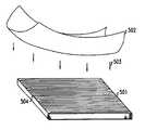
- FIG. 5shows an embodiment in accordance with the present invention wherein the substrate 502 to be imprinted with the feature pattern on stamp 501 is flexed prior to being lowered in direction 503 to make contact with feature pattern 504 .
- the features on stamp 501are smaller than 100 ⁇ m in at least one lateral dimension.
- the substrate 502is flexed axially to form a cylindrical, or approximately cylindrical, surface that is convex toward the stamp. It is beneficial to slightly raise the side edges of the substrate, thereby introducing a slight saddle shape, i.e., a very small additional convexity of the substrate toward the stamp that runs perpendicular to the main convexity.
- An alternate method of applying the substrate to the feature pattern on the stampwould be to wrap the substrate around a cylindrical roller and roll the substrate across the feature pattern.
- An exemplary substrate useful in producing electrophoretic displaysis a sheet of Mylar® material overcoated with desired layers, such as a layer of the material to be patterned by etching.
- Mylar materialhas a relatively high Young's modulus and also has a low flexural rigidity in the dimensions used herein (e.g., a thin substrate) such that the material can be flexed relatively easily.
- Young's modulusalso known as the elastic modulus, describes the elasticity of a material.
- a material, such as Mylar material, with a high Young's moduluscan be flexed with less distortion to the features on the surface of the material than a material with a low Young's modulus.
- Flexural rigiditydefines the resistance of a material to flexing.
- a material with relatively low flexural rigidity, such as thin substrate of Mylar materialcan be flexed with relative ease.
- features on the pattern-receiving surface of a Mylar material substrateare not substantially distorted during flexure of the substrate. If a substrate with a low elastic modulus is flexed in this manner to facilitate the transfer of a feature pattern, the feature pattern would be distorted during the pattern transfer process. In the case of the substrate 502 , flexing the substrate will not substantially distort the feature pattern during the pattern transfer process.
- the hereinabove described transfer of a feature patterncan also be accomplished by flexing a stamp (rather than the substrate) and then contacting the stamp and the substrate. This can be accomplished by reversing flexural rigidity properties of the stamp and the substrate, i.e., so the stamp has a low flexural rigidity relative to the substrate.
- the same transfer method described hereinabovemay be affected by flexing the stamp in a saddle or other shape, or the stamp may be applied to a cylindrical roller and rolled over a relatively rigid substrate.
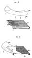
- FIG. 6shows an embodiment in accordance with the present invention wherein the substrate 602 is brought into contact with the feature pattern 504 in FIG. 5 on stamp 501 in an advantageous manner.
- the substrate 602After the substrate 602 has been flexed into a saddle shape as described above, it is brought into contact with at least one point along edge 603 of the inked surface of the stamp and is then partially unflexed to create a line of contact with edge 603 . The substrate is then permitted to flatten progressively across the stamp surface.
- the flexural rigidity of stamp 501may advantageously be higher than the substrate 602 . Flexural rigidity is a function of both the Young's (elastic) modulus and the physical dimensions of a material and is related to how easily that material is flexed. By having a stamp 501 with significantly high elastic modulus it will not distort when the substrate is brought into contact with the feature pattern 504 in FIG. 5 . Thus, the features on the stamp 501 will not shift and will be transferred accurately to the substrate 602
- a line of contact 604 between the substrate 602 and the stamp 501advances across the stamp surface in direction 605 , with full contact between the substrate and the stamp being achieved at all points behind the advancing line of contact 604 .
- a similar procedureis used in the case where the stamp is flexed, with the roles of the stamp and the substrate, as used in the procedure described hereinabove, being reversed.
- flexing the stamp or substrateis described as a method of contacting a portion of the stamp and a portion of the substrate.
- the line of contactis progressively advanced across the stamp from one side to the other.
- the stampor, alternatively, the substrate
- the stampmay be flexed in a convex manner such that the center portion of the stamp (substrate) contacts the center portion of the substrate (stamp).
- the area of contact between the stamp and the substratewould grow larger by progressively radiating in all or some directions from the center of the substrate (stamp) along the surface of the substrate (stamp). Any such method of flexing either the stamp or substrate and bringing about such advancing contact is intended to be encompassed by the present invention.
Landscapes
- Engineering & Computer Science (AREA)
- Manufacturing & Machinery (AREA)
- Microelectronics & Electronic Packaging (AREA)
- Ceramic Engineering (AREA)
- Physics & Mathematics (AREA)
- Condensed Matter Physics & Semiconductors (AREA)
- General Physics & Mathematics (AREA)
- Computer Hardware Design (AREA)
- Power Engineering (AREA)
- Manufacturing Of Printed Wiring (AREA)
Abstract
Description
Claims (12)
Priority Applications (1)
| Application Number | Priority Date | Filing Date | Title |
|---|---|---|---|
| US09/967,343US6655286B2 (en) | 2001-01-19 | 2001-09-29 | Method for preventing distortions in a flexibly transferred feature pattern |
Applications Claiming Priority (2)
| Application Number | Priority Date | Filing Date | Title |
|---|---|---|---|
| US26282101P | 2001-01-19 | 2001-01-19 | |
| US09/967,343US6655286B2 (en) | 2001-01-19 | 2001-09-29 | Method for preventing distortions in a flexibly transferred feature pattern |
Publications (2)
| Publication Number | Publication Date |
|---|---|
| US20030041762A1 US20030041762A1 (en) | 2003-03-06 |
| US6655286B2true US6655286B2 (en) | 2003-12-02 |
Family
ID=26949474
Family Applications (1)
| Application Number | Title | Priority Date | Filing Date |
|---|---|---|---|
| US09/967,343Expired - LifetimeUS6655286B2 (en) | 2001-01-19 | 2001-09-29 | Method for preventing distortions in a flexibly transferred feature pattern |
Country Status (1)
| Country | Link |
|---|---|
| US (1) | US6655286B2 (en) |
Cited By (41)
| Publication number | Priority date | Publication date | Assignee | Title |
|---|---|---|---|---|
| US20050167847A1 (en)* | 2002-06-07 | 2005-08-04 | Lennart Olsson | Method for transferring a pattern |
| US20050238967A1 (en)* | 2004-04-27 | 2005-10-27 | The Board Of Trustees Of The University Of Illinois | Composite patterning devices for soft lithography |
| US20060131266A1 (en)* | 2004-12-20 | 2006-06-22 | Palo Alto Research Center Incorporated | Large area electronic device with high and low resolution patterned film features |
| US20060286785A1 (en)* | 2004-06-04 | 2006-12-21 | The Board Of Trustees Of The University Of Illinois | A Stretchable Form of Single Crystal Silicon for High Performance Electronics on Rubber Substrates |
| US20070032089A1 (en)* | 2004-06-04 | 2007-02-08 | The Board Of Trustees Of The University Of Illinois | Printable Semiconductor Structures and Related Methods of Making and Assembling |
| US20080055581A1 (en)* | 2004-04-27 | 2008-03-06 | Rogers John A | Devices and methods for pattern generation by ink lithography |
| US20080157235A1 (en)* | 2004-06-04 | 2008-07-03 | Rogers John A | Controlled buckling structures in semiconductor interconnects and nanomembranes for stretchable electronics |
| US7557367B2 (en) | 2004-06-04 | 2009-07-07 | The Board Of Trustees Of The University Of Illinois | Stretchable semiconductor elements and stretchable electrical circuits |
| US7943491B2 (en) | 2004-06-04 | 2011-05-17 | The Board Of Trustees Of The University Of Illinois | Pattern transfer printing by kinetic control of adhesion to an elastomeric stamp |
| US7972875B2 (en) | 2007-01-17 | 2011-07-05 | The Board Of Trustees Of The University Of Illinois | Optical systems fabricated by printing-based assembly |
| US8097926B2 (en) | 2008-10-07 | 2012-01-17 | Mc10, Inc. | Systems, methods, and devices having stretchable integrated circuitry for sensing and delivering therapy |
| US8367035B2 (en) | 2006-03-03 | 2013-02-05 | The Board Of Trustees Of The University Of Illinois | Methods of making spatially aligned nanotubes and nanotube arrays |
| US8372726B2 (en) | 2008-10-07 | 2013-02-12 | Mc10, Inc. | Methods and applications of non-planar imaging arrays |
| US8389862B2 (en) | 2008-10-07 | 2013-03-05 | Mc10, Inc. | Extremely stretchable electronics |
| US8470701B2 (en) | 2008-04-03 | 2013-06-25 | Advanced Diamond Technologies, Inc. | Printable, flexible and stretchable diamond for thermal management |
| US8552299B2 (en) | 2008-03-05 | 2013-10-08 | The Board Of Trustees Of The University Of Illinois | Stretchable and foldable electronic devices |
| US8666471B2 (en) | 2010-03-17 | 2014-03-04 | The Board Of Trustees Of The University Of Illinois | Implantable biomedical devices on bioresorbable substrates |
| US8865489B2 (en) | 2009-05-12 | 2014-10-21 | The Board Of Trustees Of The University Of Illinois | Printed assemblies of ultrathin, microscale inorganic light emitting diodes for deformable and semitransparent displays |
| US8886334B2 (en) | 2008-10-07 | 2014-11-11 | Mc10, Inc. | Systems, methods, and devices using stretchable or flexible electronics for medical applications |
| US8934965B2 (en) | 2011-06-03 | 2015-01-13 | The Board Of Trustees Of The University Of Illinois | Conformable actively multiplexed high-density surface electrode array for brain interfacing |
| US8946683B2 (en) | 2008-06-16 | 2015-02-03 | The Board Of Trustees Of The University Of Illinois | Medium scale carbon nanotube thin film integrated circuits on flexible plastic substrates |
| US9159635B2 (en) | 2011-05-27 | 2015-10-13 | Mc10, Inc. | Flexible electronic structure |
| US9171794B2 (en) | 2012-10-09 | 2015-10-27 | Mc10, Inc. | Embedding thin chips in polymer |
| US9289132B2 (en) | 2008-10-07 | 2016-03-22 | Mc10, Inc. | Catheter balloon having stretchable integrated circuitry and sensor array |
| US9442285B2 (en) | 2011-01-14 | 2016-09-13 | The Board Of Trustees Of The University Of Illinois | Optical component array having adjustable curvature |
| US9554484B2 (en) | 2012-03-30 | 2017-01-24 | The Board Of Trustees Of The University Of Illinois | Appendage mountable electronic devices conformable to surfaces |
| US9691873B2 (en) | 2011-12-01 | 2017-06-27 | The Board Of Trustees Of The University Of Illinois | Transient devices designed to undergo programmable transformations |
| US9723122B2 (en) | 2009-10-01 | 2017-08-01 | Mc10, Inc. | Protective cases with integrated electronics |
| US9765934B2 (en) | 2011-05-16 | 2017-09-19 | The Board Of Trustees Of The University Of Illinois | Thermally managed LED arrays assembled by printing |
| US9936574B2 (en) | 2009-12-16 | 2018-04-03 | The Board Of Trustees Of The University Of Illinois | Waterproof stretchable optoelectronics |
| US10441185B2 (en) | 2009-12-16 | 2019-10-15 | The Board Of Trustees Of The University Of Illinois | Flexible and stretchable electronic systems for epidermal electronics |
| US10918298B2 (en) | 2009-12-16 | 2021-02-16 | The Board Of Trustees Of The University Of Illinois | High-speed, high-resolution electrophysiology in-vivo using conformal electronics |
| US10925543B2 (en) | 2015-11-11 | 2021-02-23 | The Board Of Trustees Of The University Of Illinois | Bioresorbable silicon electronics for transient implants |
| US11029198B2 (en) | 2015-06-01 | 2021-06-08 | The Board Of Trustees Of The University Of Illinois | Alternative approach for UV sensing |
| US11118965B2 (en) | 2015-06-01 | 2021-09-14 | The Board Of Trustees Of The University Of Illinois | Miniaturized electronic systems with wireless power and near-field communication capabilities |
| US11596329B2 (en) | 2016-06-17 | 2023-03-07 | The Board Of Trustees Of The University Of Illinois | Soft, wearable microfluidic systems capable of capture, storage and sensing of biofluids |
| US11660005B1 (en) | 2021-06-04 | 2023-05-30 | Huxley Medical, Inc. | Processing and analyzing biometric data |
| US11717221B1 (en) | 2020-03-11 | 2023-08-08 | Huxley Medical, Inc. | Patch for improved biometric data capture and related processes |
| US12109010B1 (en) | 2021-08-24 | 2024-10-08 | Huxley Medical, Inc. | Photoplethysmography sensors and processes |
| US12114980B1 (en) | 2021-08-24 | 2024-10-15 | Huxley Medical, Inc. | Photoplethysmography sensors and processes |
| US12178552B1 (en) | 2021-06-04 | 2024-12-31 | Huxley Medical, Inc. | Systems and processes for detecting oxygen saturation and compensating for skin tone variation |
Citations (5)
| Publication number | Priority date | Publication date | Assignee | Title |
|---|---|---|---|---|
| US4098184A (en)* | 1977-01-17 | 1978-07-04 | Honda Giken Kogyo Kabushiki Kaisha | Pressure operated flexible transfer member for screen printer |
| US5205210A (en)* | 1990-08-14 | 1993-04-27 | Walter Mathis | Method and apparatus for dry printing using a hot embossing foil |
| US5641372A (en)* | 1990-07-18 | 1997-06-24 | Nissha Printing Co., Ltd. | Transferring apparatus and transferring method |
| US5925259A (en)* | 1995-08-04 | 1999-07-20 | International Business Machines Corporation | Lithographic surface or thin layer modification |
| US6413790B1 (en)* | 1999-07-21 | 2002-07-02 | E Ink Corporation | Preferred methods for producing electrical circuit elements used to control an electronic display |
- 2001
- 2001-09-29USUS09/967,343patent/US6655286B2/ennot_activeExpired - Lifetime
Patent Citations (5)
| Publication number | Priority date | Publication date | Assignee | Title |
|---|---|---|---|---|
| US4098184A (en)* | 1977-01-17 | 1978-07-04 | Honda Giken Kogyo Kabushiki Kaisha | Pressure operated flexible transfer member for screen printer |
| US5641372A (en)* | 1990-07-18 | 1997-06-24 | Nissha Printing Co., Ltd. | Transferring apparatus and transferring method |
| US5205210A (en)* | 1990-08-14 | 1993-04-27 | Walter Mathis | Method and apparatus for dry printing using a hot embossing foil |
| US5925259A (en)* | 1995-08-04 | 1999-07-20 | International Business Machines Corporation | Lithographic surface or thin layer modification |
| US6413790B1 (en)* | 1999-07-21 | 2002-07-02 | E Ink Corporation | Preferred methods for producing electrical circuit elements used to control an electronic display |
Cited By (96)
| Publication number | Priority date | Publication date | Assignee | Title |
|---|---|---|---|---|
| US20050167847A1 (en)* | 2002-06-07 | 2005-08-04 | Lennart Olsson | Method for transferring a pattern |
| US7082876B2 (en)* | 2002-06-07 | 2006-08-01 | Obducat Ab | Method for transferring a pattern |
| US7195733B2 (en) | 2004-04-27 | 2007-03-27 | The Board Of Trustees Of The University Of Illinois | Composite patterning devices for soft lithography |
| US20050238967A1 (en)* | 2004-04-27 | 2005-10-27 | The Board Of Trustees Of The University Of Illinois | Composite patterning devices for soft lithography |
| US20080055581A1 (en)* | 2004-04-27 | 2008-03-06 | Rogers John A | Devices and methods for pattern generation by ink lithography |
| US8440546B2 (en) | 2004-06-04 | 2013-05-14 | The Board Of Trustees Of The University Of Illinois | Methods and devices for fabricating and assembling printable semiconductor elements |
| US7943491B2 (en) | 2004-06-04 | 2011-05-17 | The Board Of Trustees Of The University Of Illinois | Pattern transfer printing by kinetic control of adhesion to an elastomeric stamp |
| US20060286785A1 (en)* | 2004-06-04 | 2006-12-21 | The Board Of Trustees Of The University Of Illinois | A Stretchable Form of Single Crystal Silicon for High Performance Electronics on Rubber Substrates |
| US9768086B2 (en) | 2004-06-04 | 2017-09-19 | The Board Of Trustees Of The University Of Illinois | Methods and devices for fabricating and assembling printable semiconductor elements |
| US20080157235A1 (en)* | 2004-06-04 | 2008-07-03 | Rogers John A | Controlled buckling structures in semiconductor interconnects and nanomembranes for stretchable electronics |
| US7521292B2 (en) | 2004-06-04 | 2009-04-21 | The Board Of Trustees Of The University Of Illinois | Stretchable form of single crystal silicon for high performance electronics on rubber substrates |
| US7557367B2 (en) | 2004-06-04 | 2009-07-07 | The Board Of Trustees Of The University Of Illinois | Stretchable semiconductor elements and stretchable electrical circuits |
| US7622367B1 (en) | 2004-06-04 | 2009-11-24 | The Board Of Trustees Of The University Of Illinois | Methods and devices for fabricating and assembling printable semiconductor elements |
| US20090294803A1 (en)* | 2004-06-04 | 2009-12-03 | The Board Of Trustees Of The University Of Illinois | Methods and devices for fabricating and assembling printable semiconductor elements |
| US9515025B2 (en) | 2004-06-04 | 2016-12-06 | The Board Of Trustees Of The University Of Illinois | Stretchable form of single crystal silicon for high performance electronics on rubber substrates |
| US11456258B2 (en) | 2004-06-04 | 2022-09-27 | The Board Of Trustees Of The University Of Illinois | Stretchable form of single crystal silicon for high performance electronics on rubber substrates |
| US9450043B2 (en) | 2004-06-04 | 2016-09-20 | The Board Of Trustees Of The University Of Illinois | Methods and devices for fabricating and assembling printable semiconductor elements |
| US7982296B2 (en) | 2004-06-04 | 2011-07-19 | The Board Of Trustees Of The University Of Illinois | Methods and devices for fabricating and assembling printable semiconductor elements |
| US8039847B2 (en) | 2004-06-04 | 2011-10-18 | The Board Of Trustees Of The University Of Illinois | Printable semiconductor structures and related methods of making and assembling |
| US10204864B2 (en) | 2004-06-04 | 2019-02-12 | The Board Of Trustees Of The University Of Illinois | Stretchable form of single crystal silicon for high performance electronics on rubber substrates |
| US8198621B2 (en) | 2004-06-04 | 2012-06-12 | The Board Of Trustees Of The University Of Illinois | Stretchable form of single crystal silicon for high performance electronics on rubber substrates |
| US8217381B2 (en) | 2004-06-04 | 2012-07-10 | The Board Of Trustees Of The University Of Illinois | Controlled buckling structures in semiconductor interconnects and nanomembranes for stretchable electronics |
| US9324733B2 (en) | 2004-06-04 | 2016-04-26 | The Board Of Trustees Of The University Of Illinois | Controlled buckling structures in semiconductor interconnects and nanomembranes for stretchable electronics |
| US10355113B2 (en) | 2004-06-04 | 2019-07-16 | The Board Of Trustees Of The University Of Illinois | Controlled buckling structures in semiconductor interconnects and nanomembranes for stretchable electronics |
| US12074213B2 (en) | 2004-06-04 | 2024-08-27 | The Board Of Trustees Of The University Of Illinois | Methods and devices for fabricating and assembling printable semiconductor elements |
| US8394706B2 (en) | 2004-06-04 | 2013-03-12 | The Board Of Trustees Of The University Of Illinois | Printable semiconductor structures and related methods of making and assembling |
| US9761444B2 (en) | 2004-06-04 | 2017-09-12 | The Board Of Trustees Of The University Of Illinois | Methods and devices for fabricating and assembling printable semiconductor elements |
| US20070032089A1 (en)* | 2004-06-04 | 2007-02-08 | The Board Of Trustees Of The University Of Illinois | Printable Semiconductor Structures and Related Methods of Making and Assembling |
| US9105555B2 (en) | 2004-06-04 | 2015-08-11 | The Board Of Trustees Of The University Of Illinois | Stretchable form of single crystal silicon for high performance electronics on rubber substrates |
| US7799699B2 (en) | 2004-06-04 | 2010-09-21 | The Board Of Trustees Of The University Of Illinois | Printable semiconductor structures and related methods of making and assembling |
| US8664699B2 (en) | 2004-06-04 | 2014-03-04 | The Board Of Trustees Of The University Of Illinois | Methods and devices for fabricating and assembling printable semiconductor elements |
| US10374072B2 (en) | 2004-06-04 | 2019-08-06 | The Board Of Trustees Of The University Of Illinois | Methods and devices for fabricating and assembling printable semiconductor elements |
| US11088268B2 (en) | 2004-06-04 | 2021-08-10 | The Board Of Trustees Of The University Of Illinois | Methods and devices for fabricating and assembling printable semiconductor elements |
| US8729524B2 (en) | 2004-06-04 | 2014-05-20 | The Board Of Trustees Of The University Of Illinois | Controlled buckling structures in semiconductor interconnects and nanomembranes for stretchable electronics |
| US8754396B2 (en) | 2004-06-04 | 2014-06-17 | The Board Of Trustees Of The University Of Illinois | Stretchable form of single crystal silicon for high performance electronics on rubber substrates |
| US20060131266A1 (en)* | 2004-12-20 | 2006-06-22 | Palo Alto Research Center Incorporated | Large area electronic device with high and low resolution patterned film features |
| US7125495B2 (en) | 2004-12-20 | 2006-10-24 | Palo Alto Research Center, Inc. | Large area electronic device with high and low resolution patterned film features |
| US8367035B2 (en) | 2006-03-03 | 2013-02-05 | The Board Of Trustees Of The University Of Illinois | Methods of making spatially aligned nanotubes and nanotube arrays |
| US12136620B2 (en) | 2007-01-17 | 2024-11-05 | The Board Of Trustees Of The University Of Illinois | Optical systems fabricated by printing-based assembly |
| US7972875B2 (en) | 2007-01-17 | 2011-07-05 | The Board Of Trustees Of The University Of Illinois | Optical systems fabricated by printing-based assembly |
| US11309305B2 (en) | 2007-01-17 | 2022-04-19 | The Board Of Trustees Of The University Of Illinois | Optical systems fabricated by printing-based assembly |
| US9601671B2 (en) | 2007-01-17 | 2017-03-21 | The Board Of Trustees Of The University Of Illinois | Optical systems fabricated by printing-based assembly |
| US8722458B2 (en) | 2007-01-17 | 2014-05-13 | The Board Of Trustees Of The University Of Illinois | Optical systems fabricated by printing-based assembly |
| US10424572B2 (en) | 2007-01-17 | 2019-09-24 | The Board Of Trustees Of The University Of Illinois | Optical systems fabricated by printing-based assembly |
| US10504882B2 (en) | 2007-01-17 | 2019-12-10 | The Board Of Trustees Of The University Of Illinois | Optical systems fabricated by printing-based assembly |
| US9117940B2 (en) | 2007-01-17 | 2015-08-25 | The Board Of Trustees Of The University Of Illinois | Optical systems fabricated by printing-based assembly |
| US10361180B2 (en) | 2007-01-17 | 2019-07-23 | The Board Of Trustees Of The University Of Illinois | Optical systems fabricated by printing-based assembly |
| US10292261B2 (en) | 2008-03-05 | 2019-05-14 | The Board Of Trustees Of The University Of Illinois | Stretchable and foldable electronic devices |
| US10064269B2 (en) | 2008-03-05 | 2018-08-28 | The Board Of Trustees Of The University Of Illinois | Stretchable and foldable electronic devices |
| US8552299B2 (en) | 2008-03-05 | 2013-10-08 | The Board Of Trustees Of The University Of Illinois | Stretchable and foldable electronic devices |
| US8905772B2 (en) | 2008-03-05 | 2014-12-09 | The Board Of Trustees Of The University Of Illinois | Stretchable and foldable electronic devices |
| US8470701B2 (en) | 2008-04-03 | 2013-06-25 | Advanced Diamond Technologies, Inc. | Printable, flexible and stretchable diamond for thermal management |
| US8946683B2 (en) | 2008-06-16 | 2015-02-03 | The Board Of Trustees Of The University Of Illinois | Medium scale carbon nanotube thin film integrated circuits on flexible plastic substrates |
| US8372726B2 (en) | 2008-10-07 | 2013-02-12 | Mc10, Inc. | Methods and applications of non-planar imaging arrays |
| US9516758B2 (en) | 2008-10-07 | 2016-12-06 | Mc10, Inc. | Extremely stretchable electronics |
| US8097926B2 (en) | 2008-10-07 | 2012-01-17 | Mc10, Inc. | Systems, methods, and devices having stretchable integrated circuitry for sensing and delivering therapy |
| US8389862B2 (en) | 2008-10-07 | 2013-03-05 | Mc10, Inc. | Extremely stretchable electronics |
| US8536667B2 (en) | 2008-10-07 | 2013-09-17 | Mc10, Inc. | Systems, methods, and devices having stretchable integrated circuitry for sensing and delivering therapy |
| US8886334B2 (en) | 2008-10-07 | 2014-11-11 | Mc10, Inc. | Systems, methods, and devices using stretchable or flexible electronics for medical applications |
| US9012784B2 (en) | 2008-10-07 | 2015-04-21 | Mc10, Inc. | Extremely stretchable electronics |
| US9289132B2 (en) | 2008-10-07 | 2016-03-22 | Mc10, Inc. | Catheter balloon having stretchable integrated circuitry and sensor array |
| US10546841B2 (en) | 2009-05-12 | 2020-01-28 | The Board Of Trustees Of The University Of Illinois | Printed assemblies of ultrathin, microscale inorganic light emitting diodes for deformable and semitransparent displays |
| US8865489B2 (en) | 2009-05-12 | 2014-10-21 | The Board Of Trustees Of The University Of Illinois | Printed assemblies of ultrathin, microscale inorganic light emitting diodes for deformable and semitransparent displays |
| US9647171B2 (en) | 2009-05-12 | 2017-05-09 | The Board Of Trustees Of The University Of Illinois | Printed assemblies of ultrathin, microscale inorganic light emitting diodes for deformable and semitransparent displays |
| US9723122B2 (en) | 2009-10-01 | 2017-08-01 | Mc10, Inc. | Protective cases with integrated electronics |
| US11057991B2 (en) | 2009-12-16 | 2021-07-06 | The Board Of Trustees Of The University Of Illinois | Waterproof stretchable optoelectronics |
| US9936574B2 (en) | 2009-12-16 | 2018-04-03 | The Board Of Trustees Of The University Of Illinois | Waterproof stretchable optoelectronics |
| US10441185B2 (en) | 2009-12-16 | 2019-10-15 | The Board Of Trustees Of The University Of Illinois | Flexible and stretchable electronic systems for epidermal electronics |
| US10918298B2 (en) | 2009-12-16 | 2021-02-16 | The Board Of Trustees Of The University Of Illinois | High-speed, high-resolution electrophysiology in-vivo using conformal electronics |
| US9986924B2 (en) | 2010-03-17 | 2018-06-05 | The Board Of Trustees Of The University Of Illinois | Implantable biomedical devices on bioresorbable substrates |
| US8666471B2 (en) | 2010-03-17 | 2014-03-04 | The Board Of Trustees Of The University Of Illinois | Implantable biomedical devices on bioresorbable substrates |
| US9442285B2 (en) | 2011-01-14 | 2016-09-13 | The Board Of Trustees Of The University Of Illinois | Optical component array having adjustable curvature |
| US9765934B2 (en) | 2011-05-16 | 2017-09-19 | The Board Of Trustees Of The University Of Illinois | Thermally managed LED arrays assembled by printing |
| US9159635B2 (en) | 2011-05-27 | 2015-10-13 | Mc10, Inc. | Flexible electronic structure |
| US10349860B2 (en) | 2011-06-03 | 2019-07-16 | The Board Of Trustees Of The University Of Illinois | Conformable actively multiplexed high-density surface electrode array for brain interfacing |
| US8934965B2 (en) | 2011-06-03 | 2015-01-13 | The Board Of Trustees Of The University Of Illinois | Conformable actively multiplexed high-density surface electrode array for brain interfacing |
| US10396173B2 (en) | 2011-12-01 | 2019-08-27 | The Board Of Trustees Of The University Of Illinois | Transient devices designed to undergo programmable transformations |
| US9691873B2 (en) | 2011-12-01 | 2017-06-27 | The Board Of Trustees Of The University Of Illinois | Transient devices designed to undergo programmable transformations |
| US9554484B2 (en) | 2012-03-30 | 2017-01-24 | The Board Of Trustees Of The University Of Illinois | Appendage mountable electronic devices conformable to surfaces |
| US10052066B2 (en) | 2012-03-30 | 2018-08-21 | The Board Of Trustees Of The University Of Illinois | Appendage mountable electronic devices conformable to surfaces |
| US10357201B2 (en) | 2012-03-30 | 2019-07-23 | The Board Of Trustees Of The University Of Illinois | Appendage mountable electronic devices conformable to surfaces |
| US9171794B2 (en) | 2012-10-09 | 2015-10-27 | Mc10, Inc. | Embedding thin chips in polymer |
| US11029198B2 (en) | 2015-06-01 | 2021-06-08 | The Board Of Trustees Of The University Of Illinois | Alternative approach for UV sensing |
| US11118965B2 (en) | 2015-06-01 | 2021-09-14 | The Board Of Trustees Of The University Of Illinois | Miniaturized electronic systems with wireless power and near-field communication capabilities |
| US10925543B2 (en) | 2015-11-11 | 2021-02-23 | The Board Of Trustees Of The University Of Illinois | Bioresorbable silicon electronics for transient implants |
| US11596329B2 (en) | 2016-06-17 | 2023-03-07 | The Board Of Trustees Of The University Of Illinois | Soft, wearable microfluidic systems capable of capture, storage and sensing of biofluids |
| US12171576B1 (en) | 2020-03-11 | 2024-12-24 | Huxley Medical, Inc. | Patch for improved biometric data capture and related processes |
| US11717221B1 (en) | 2020-03-11 | 2023-08-08 | Huxley Medical, Inc. | Patch for improved biometric data capture and related processes |
| US12076117B1 (en) | 2021-06-04 | 2024-09-03 | Huxley Medical, Inc. | Processing and analyzing biometric data |
| US11660005B1 (en) | 2021-06-04 | 2023-05-30 | Huxley Medical, Inc. | Processing and analyzing biometric data |
| US12178552B1 (en) | 2021-06-04 | 2024-12-31 | Huxley Medical, Inc. | Systems and processes for detecting oxygen saturation and compensating for skin tone variation |
| US12329497B1 (en) | 2021-06-04 | 2025-06-17 | Huxley Medical, Inc. | Processing and analyzing biometric data |
| US12109010B1 (en) | 2021-08-24 | 2024-10-08 | Huxley Medical, Inc. | Photoplethysmography sensors and processes |
| US12114980B1 (en) | 2021-08-24 | 2024-10-15 | Huxley Medical, Inc. | Photoplethysmography sensors and processes |
| US12279853B1 (en) | 2021-08-24 | 2025-04-22 | Huxley Medical, Inc. | Photoplethysmography sensors and processes |
| US12414699B1 (en) | 2021-08-24 | 2025-09-16 | Huxley Medical, Inc. | Photoplethysmography sensors and processes |
Also Published As
| Publication number | Publication date |
|---|---|
| US20030041762A1 (en) | 2003-03-06 |
Similar Documents
| Publication | Publication Date | Title |
|---|---|---|
| US6655286B2 (en) | Method for preventing distortions in a flexibly transferred feature pattern | |
| US8291820B2 (en) | Intaglio printing plate, production method for intaglio printing plate, production method for electronic substrate, and production method for display device | |
| JP2008246829A (en) | Printing plate for letterpress reverse offset printing, method for manufacturing the same, display device, and method for manufacturing substrate for display device | |
| JP2702068B2 (en) | Method of forming thin film transistor circuit by offset printing method | |
| EP1939006B1 (en) | Method of printing | |
| EP2762313B1 (en) | Cliche for offset-printing and method for manufacturing same | |
| KR100825476B1 (en) | Fine pattern printing method | |
| US20020098618A1 (en) | Method and apparatus for transferring a feature pattern from an inked surface to a substrate | |
| JP2010058330A (en) | Method for forming image pattern and image pattern and semiconductor device, electric circuit, display module, color filter, and light emitting element | |
| US20030041761A1 (en) | Method for removing unwanted particles from a surface used in the process of flexibly transferring a feature pattern from an inked surface to a substrate | |
| JP2004017409A (en) | Letterpress and pattern forming method | |
| KR20180039228A (en) | Method of manufacturing display apparatus | |
| JPH04239684A (en) | Method for forming of fine pattern | |
| US11541676B2 (en) | Positioning aid for a stamping tool | |
| JP2012071506A (en) | Device and method for forming pattern | |
| KR20100072969A (en) | Method of fabricating cliche for roll print and method of fabricating liquid crystal display device using thereof | |
| CN100429568C (en) | Printing apparatus and fabricating method thereof | |
| CN100553971C (en) | Method and apparatus for printing a patterned layer on a flat substrate using a flat bed machine | |
| KR102113903B1 (en) | Method for manufacturing cliche for offset printing and cliche for offset printing | |
| Chang et al. | 43.1: Distinguished Paper: Design Parameters of Roll Printing Process for TFT‐LCD Fabrication | |
| Chang et al. | A study of roll‐printing technology for TFT‐LCD fabrication | |
| CN207623679U (en) | A kind of nano-imprint stamp | |
| KR101186520B1 (en) | Method on mold fabricating for formatting pattern and thin film transistor- crystal display device using it | |
| JP2000238402A (en) | Printing substrate, printed matter, and high-definition printing method | |
| KR102016616B1 (en) | Method for manufacturing cliche for offset printing and cliche for offset printing |
Legal Events
| Date | Code | Title | Description |
|---|---|---|---|
| AS | Assignment | Owner name:LUCENT TECHNOLOGIES INC., NEW JERSEY Free format text:ASSIGNMENT OF ASSIGNORS INTEREST;ASSIGNOR:ROGERS, JOHN A.;REEL/FRAME:012220/0335 Effective date:20010928 | |
| STCF | Information on status: patent grant | Free format text:PATENTED CASE | |
| FEPP | Fee payment procedure | Free format text:PAYOR NUMBER ASSIGNED (ORIGINAL EVENT CODE: ASPN); ENTITY STATUS OF PATENT OWNER: LARGE ENTITY | |
| FPAY | Fee payment | Year of fee payment:4 | |
| FPAY | Fee payment | Year of fee payment:8 | |
| AS | Assignment | Owner name:CREDIT SUISSE AG, NEW YORK Free format text:SECURITY INTEREST;ASSIGNOR:ALCATEL-LUCENT USA INC.;REEL/FRAME:030510/0627 Effective date:20130130 | |
| AS | Assignment | Owner name:ALCATEL-LUCENT USA INC., NEW JERSEY Free format text:RELEASE BY SECURED PARTY;ASSIGNOR:CREDIT SUISSE AG;REEL/FRAME:033950/0261 Effective date:20140819 | |
| FPAY | Fee payment | Year of fee payment:12 | |
| AS | Assignment | Owner name:OMEGA CREDIT OPPORTUNITIES MASTER FUND, LP, NEW YORK Free format text:SECURITY INTEREST;ASSIGNOR:WSOU INVESTMENTS, LLC;REEL/FRAME:043966/0574 Effective date:20170822 Owner name:OMEGA CREDIT OPPORTUNITIES MASTER FUND, LP, NEW YO Free format text:SECURITY INTEREST;ASSIGNOR:WSOU INVESTMENTS, LLC;REEL/FRAME:043966/0574 Effective date:20170822 | |
| AS | Assignment | Owner name:WSOU INVESTMENTS, LLC, CALIFORNIA Free format text:ASSIGNMENT OF ASSIGNORS INTEREST;ASSIGNOR:ALCATEL LUCENT;REEL/FRAME:044000/0053 Effective date:20170722 | |
| AS | Assignment | Owner name:BP FUNDING TRUST, SERIES SPL-VI, NEW YORK Free format text:SECURITY INTEREST;ASSIGNOR:WSOU INVESTMENTS, LLC;REEL/FRAME:049235/0068 Effective date:20190516 | |
| AS | Assignment | Owner name:WSOU INVESTMENTS, LLC, CALIFORNIA Free format text:RELEASE BY SECURED PARTY;ASSIGNOR:OCO OPPORTUNITIES MASTER FUND, L.P. (F/K/A OMEGA CREDIT OPPORTUNITIES MASTER FUND LP;REEL/FRAME:049246/0405 Effective date:20190516 | |
| AS | Assignment | Owner name:OT WSOU TERRIER HOLDINGS, LLC, CALIFORNIA Free format text:SECURITY INTEREST;ASSIGNOR:WSOU INVESTMENTS, LLC;REEL/FRAME:056990/0081 Effective date:20210528 | |
| AS | Assignment | Owner name:WSOU INVESTMENTS, LLC, CALIFORNIA Free format text:RELEASE BY SECURED PARTY;ASSIGNOR:TERRIER SSC, LLC;REEL/FRAME:056526/0093 Effective date:20210528 |