US6653721B2 - LOC semiconductor assembled with room temperature adhesive - Google Patents
LOC semiconductor assembled with room temperature adhesiveDownload PDFInfo
- Publication number
- US6653721B2 US6653721B2US09/942,140US94214001AUS6653721B2US 6653721 B2US6653721 B2US 6653721B2US 94214001 AUS94214001 AUS 94214001AUS 6653721 B2US6653721 B2US 6653721B2
- Authority
- US
- United States
- Prior art keywords
- semiconductor device
- lead frame
- percent
- lead
- adhesive
- Prior art date
- Legal status (The legal status is an assumption and is not a legal conclusion. Google has not performed a legal analysis and makes no representation as to the accuracy of the status listed.)
- Expired - Lifetime
Links
Images


Classifications
- H—ELECTRICITY
- H01—ELECTRIC ELEMENTS
- H01L—SEMICONDUCTOR DEVICES NOT COVERED BY CLASS H10
- H01L24/00—Arrangements for connecting or disconnecting semiconductor or solid-state bodies; Methods or apparatus related thereto
- H01L24/01—Means for bonding being attached to, or being formed on, the surface to be connected, e.g. chip-to-package, die-attach, "first-level" interconnects; Manufacturing methods related thereto
- H01L24/26—Layer connectors, e.g. plate connectors, solder or adhesive layers; Manufacturing methods related thereto
- H01L24/27—Manufacturing methods
- H—ELECTRICITY
- H01—ELECTRIC ELEMENTS
- H01L—SEMICONDUCTOR DEVICES NOT COVERED BY CLASS H10
- H01L23/00—Details of semiconductor or other solid state devices
- H01L23/48—Arrangements for conducting electric current to or from the solid state body in operation, e.g. leads, terminal arrangements ; Selection of materials therefor
- H01L23/488—Arrangements for conducting electric current to or from the solid state body in operation, e.g. leads, terminal arrangements ; Selection of materials therefor consisting of soldered or bonded constructions
- H01L23/495—Lead-frames or other flat leads
- H01L23/49503—Lead-frames or other flat leads characterised by the die pad
- H01L23/4951—Chip-on-leads or leads-on-chip techniques, i.e. inner lead fingers being used as die pad
- H—ELECTRICITY
- H01—ELECTRIC ELEMENTS
- H01L—SEMICONDUCTOR DEVICES NOT COVERED BY CLASS H10
- H01L23/00—Details of semiconductor or other solid state devices
- H01L23/48—Arrangements for conducting electric current to or from the solid state body in operation, e.g. leads, terminal arrangements ; Selection of materials therefor
- H01L23/488—Arrangements for conducting electric current to or from the solid state body in operation, e.g. leads, terminal arrangements ; Selection of materials therefor consisting of soldered or bonded constructions
- H01L23/495—Lead-frames or other flat leads
- H01L23/49503—Lead-frames or other flat leads characterised by the die pad
- H01L23/49513—Lead-frames or other flat leads characterised by the die pad having bonding material between chip and die pad
- H—ELECTRICITY
- H01—ELECTRIC ELEMENTS
- H01L—SEMICONDUCTOR DEVICES NOT COVERED BY CLASS H10
- H01L24/00—Arrangements for connecting or disconnecting semiconductor or solid-state bodies; Methods or apparatus related thereto
- H01L24/01—Means for bonding being attached to, or being formed on, the surface to be connected, e.g. chip-to-package, die-attach, "first-level" interconnects; Manufacturing methods related thereto
- H01L24/26—Layer connectors, e.g. plate connectors, solder or adhesive layers; Manufacturing methods related thereto
- H01L24/28—Structure, shape, material or disposition of the layer connectors prior to the connecting process
- H01L24/29—Structure, shape, material or disposition of the layer connectors prior to the connecting process of an individual layer connector
- H—ELECTRICITY
- H01—ELECTRIC ELEMENTS
- H01L—SEMICONDUCTOR DEVICES NOT COVERED BY CLASS H10
- H01L24/00—Arrangements for connecting or disconnecting semiconductor or solid-state bodies; Methods or apparatus related thereto
- H01L24/01—Means for bonding being attached to, or being formed on, the surface to be connected, e.g. chip-to-package, die-attach, "first-level" interconnects; Manufacturing methods related thereto
- H01L24/26—Layer connectors, e.g. plate connectors, solder or adhesive layers; Manufacturing methods related thereto
- H01L24/31—Structure, shape, material or disposition of the layer connectors after the connecting process
- H01L24/32—Structure, shape, material or disposition of the layer connectors after the connecting process of an individual layer connector
- H—ELECTRICITY
- H01—ELECTRIC ELEMENTS
- H01L—SEMICONDUCTOR DEVICES NOT COVERED BY CLASS H10
- H01L24/00—Arrangements for connecting or disconnecting semiconductor or solid-state bodies; Methods or apparatus related thereto
- H01L24/74—Apparatus for manufacturing arrangements for connecting or disconnecting semiconductor or solid-state bodies
- H01L24/741—Apparatus for manufacturing means for bonding, e.g. connectors
- H01L24/743—Apparatus for manufacturing layer connectors
- H—ELECTRICITY
- H01—ELECTRIC ELEMENTS
- H01L—SEMICONDUCTOR DEVICES NOT COVERED BY CLASS H10
- H01L24/00—Arrangements for connecting or disconnecting semiconductor or solid-state bodies; Methods or apparatus related thereto
- H01L24/80—Methods for connecting semiconductor or other solid state bodies using means for bonding being attached to, or being formed on, the surface to be connected
- H01L24/83—Methods for connecting semiconductor or other solid state bodies using means for bonding being attached to, or being formed on, the surface to be connected using a layer connector
- H—ELECTRICITY
- H01—ELECTRIC ELEMENTS
- H01L—SEMICONDUCTOR DEVICES NOT COVERED BY CLASS H10
- H01L2224/00—Indexing scheme for arrangements for connecting or disconnecting semiconductor or solid-state bodies and methods related thereto as covered by H01L24/00
- H01L2224/01—Means for bonding being attached to, or being formed on, the surface to be connected, e.g. chip-to-package, die-attach, "first-level" interconnects; Manufacturing methods related thereto
- H01L2224/26—Layer connectors, e.g. plate connectors, solder or adhesive layers; Manufacturing methods related thereto
- H01L2224/31—Structure, shape, material or disposition of the layer connectors after the connecting process
- H01L2224/32—Structure, shape, material or disposition of the layer connectors after the connecting process of an individual layer connector
- H01L2224/3201—Structure
- H01L2224/32012—Structure relative to the bonding area, e.g. bond pad
- H01L2224/32014—Structure relative to the bonding area, e.g. bond pad the layer connector being smaller than the bonding area, e.g. bond pad
- H—ELECTRICITY
- H01—ELECTRIC ELEMENTS
- H01L—SEMICONDUCTOR DEVICES NOT COVERED BY CLASS H10
- H01L2224/00—Indexing scheme for arrangements for connecting or disconnecting semiconductor or solid-state bodies and methods related thereto as covered by H01L24/00
- H01L2224/01—Means for bonding being attached to, or being formed on, the surface to be connected, e.g. chip-to-package, die-attach, "first-level" interconnects; Manufacturing methods related thereto
- H01L2224/26—Layer connectors, e.g. plate connectors, solder or adhesive layers; Manufacturing methods related thereto
- H01L2224/31—Structure, shape, material or disposition of the layer connectors after the connecting process
- H01L2224/32—Structure, shape, material or disposition of the layer connectors after the connecting process of an individual layer connector
- H01L2224/321—Disposition
- H01L2224/32151—Disposition the layer connector connecting between a semiconductor or solid-state body and an item not being a semiconductor or solid-state body, e.g. chip-to-substrate, chip-to-passive
- H01L2224/32221—Disposition the layer connector connecting between a semiconductor or solid-state body and an item not being a semiconductor or solid-state body, e.g. chip-to-substrate, chip-to-passive the body and the item being stacked
- H01L2224/32245—Disposition the layer connector connecting between a semiconductor or solid-state body and an item not being a semiconductor or solid-state body, e.g. chip-to-substrate, chip-to-passive the body and the item being stacked the item being metallic
- H—ELECTRICITY
- H01—ELECTRIC ELEMENTS
- H01L—SEMICONDUCTOR DEVICES NOT COVERED BY CLASS H10
- H01L2224/00—Indexing scheme for arrangements for connecting or disconnecting semiconductor or solid-state bodies and methods related thereto as covered by H01L24/00
- H01L2224/01—Means for bonding being attached to, or being formed on, the surface to be connected, e.g. chip-to-package, die-attach, "first-level" interconnects; Manufacturing methods related thereto
- H01L2224/42—Wire connectors; Manufacturing methods related thereto
- H01L2224/47—Structure, shape, material or disposition of the wire connectors after the connecting process
- H01L2224/48—Structure, shape, material or disposition of the wire connectors after the connecting process of an individual wire connector
- H01L2224/4805—Shape
- H01L2224/4809—Loop shape
- H01L2224/48091—Arched
- H—ELECTRICITY
- H01—ELECTRIC ELEMENTS
- H01L—SEMICONDUCTOR DEVICES NOT COVERED BY CLASS H10
- H01L2224/00—Indexing scheme for arrangements for connecting or disconnecting semiconductor or solid-state bodies and methods related thereto as covered by H01L24/00
- H01L2224/01—Means for bonding being attached to, or being formed on, the surface to be connected, e.g. chip-to-package, die-attach, "first-level" interconnects; Manufacturing methods related thereto
- H01L2224/42—Wire connectors; Manufacturing methods related thereto
- H01L2224/47—Structure, shape, material or disposition of the wire connectors after the connecting process
- H01L2224/48—Structure, shape, material or disposition of the wire connectors after the connecting process of an individual wire connector
- H01L2224/481—Disposition
- H01L2224/48151—Connecting between a semiconductor or solid-state body and an item not being a semiconductor or solid-state body, e.g. chip-to-substrate, chip-to-passive
- H01L2224/48221—Connecting between a semiconductor or solid-state body and an item not being a semiconductor or solid-state body, e.g. chip-to-substrate, chip-to-passive the body and the item being stacked
- H01L2224/48225—Connecting between a semiconductor or solid-state body and an item not being a semiconductor or solid-state body, e.g. chip-to-substrate, chip-to-passive the body and the item being stacked the item being non-metallic, e.g. insulating substrate with or without metallisation
- H01L2224/4824—Connecting between the body and an opposite side of the item with respect to the body
- H—ELECTRICITY
- H01—ELECTRIC ELEMENTS
- H01L—SEMICONDUCTOR DEVICES NOT COVERED BY CLASS H10
- H01L2224/00—Indexing scheme for arrangements for connecting or disconnecting semiconductor or solid-state bodies and methods related thereto as covered by H01L24/00
- H01L2224/01—Means for bonding being attached to, or being formed on, the surface to be connected, e.g. chip-to-package, die-attach, "first-level" interconnects; Manufacturing methods related thereto
- H01L2224/42—Wire connectors; Manufacturing methods related thereto
- H01L2224/47—Structure, shape, material or disposition of the wire connectors after the connecting process
- H01L2224/48—Structure, shape, material or disposition of the wire connectors after the connecting process of an individual wire connector
- H01L2224/481—Disposition
- H01L2224/48151—Connecting between a semiconductor or solid-state body and an item not being a semiconductor or solid-state body, e.g. chip-to-substrate, chip-to-passive
- H01L2224/48221—Connecting between a semiconductor or solid-state body and an item not being a semiconductor or solid-state body, e.g. chip-to-substrate, chip-to-passive the body and the item being stacked
- H01L2224/48245—Connecting between a semiconductor or solid-state body and an item not being a semiconductor or solid-state body, e.g. chip-to-substrate, chip-to-passive the body and the item being stacked the item being metallic
- H01L2224/48247—Connecting between a semiconductor or solid-state body and an item not being a semiconductor or solid-state body, e.g. chip-to-substrate, chip-to-passive the body and the item being stacked the item being metallic connecting the wire to a bond pad of the item
- H—ELECTRICITY
- H01—ELECTRIC ELEMENTS
- H01L—SEMICONDUCTOR DEVICES NOT COVERED BY CLASS H10
- H01L2224/00—Indexing scheme for arrangements for connecting or disconnecting semiconductor or solid-state bodies and methods related thereto as covered by H01L24/00
- H01L2224/01—Means for bonding being attached to, or being formed on, the surface to be connected, e.g. chip-to-package, die-attach, "first-level" interconnects; Manufacturing methods related thereto
- H01L2224/42—Wire connectors; Manufacturing methods related thereto
- H01L2224/47—Structure, shape, material or disposition of the wire connectors after the connecting process
- H01L2224/48—Structure, shape, material or disposition of the wire connectors after the connecting process of an individual wire connector
- H01L2224/481—Disposition
- H01L2224/48151—Connecting between a semiconductor or solid-state body and an item not being a semiconductor or solid-state body, e.g. chip-to-substrate, chip-to-passive
- H01L2224/48221—Connecting between a semiconductor or solid-state body and an item not being a semiconductor or solid-state body, e.g. chip-to-substrate, chip-to-passive the body and the item being stacked
- H01L2224/48245—Connecting between a semiconductor or solid-state body and an item not being a semiconductor or solid-state body, e.g. chip-to-substrate, chip-to-passive the body and the item being stacked the item being metallic
- H01L2224/4826—Connecting between the body and an opposite side of the item with respect to the body
- H—ELECTRICITY
- H01—ELECTRIC ELEMENTS
- H01L—SEMICONDUCTOR DEVICES NOT COVERED BY CLASS H10
- H01L2224/00—Indexing scheme for arrangements for connecting or disconnecting semiconductor or solid-state bodies and methods related thereto as covered by H01L24/00
- H01L2224/01—Means for bonding being attached to, or being formed on, the surface to be connected, e.g. chip-to-package, die-attach, "first-level" interconnects; Manufacturing methods related thereto
- H01L2224/42—Wire connectors; Manufacturing methods related thereto
- H01L2224/47—Structure, shape, material or disposition of the wire connectors after the connecting process
- H01L2224/48—Structure, shape, material or disposition of the wire connectors after the connecting process of an individual wire connector
- H01L2224/484—Connecting portions
- H01L2224/48463—Connecting portions the connecting portion on the bonding area of the semiconductor or solid-state body being a ball bond
- H01L2224/48465—Connecting portions the connecting portion on the bonding area of the semiconductor or solid-state body being a ball bond the other connecting portion not on the bonding area being a wedge bond, i.e. ball-to-wedge, regular stitch
- H—ELECTRICITY
- H01—ELECTRIC ELEMENTS
- H01L—SEMICONDUCTOR DEVICES NOT COVERED BY CLASS H10
- H01L2224/00—Indexing scheme for arrangements for connecting or disconnecting semiconductor or solid-state bodies and methods related thereto as covered by H01L24/00
- H01L2224/73—Means for bonding being of different types provided for in two or more of groups H01L2224/10, H01L2224/18, H01L2224/26, H01L2224/34, H01L2224/42, H01L2224/50, H01L2224/63, H01L2224/71
- H01L2224/732—Location after the connecting process
- H01L2224/73201—Location after the connecting process on the same surface
- H01L2224/73215—Layer and wire connectors
- H—ELECTRICITY
- H01—ELECTRIC ELEMENTS
- H01L—SEMICONDUCTOR DEVICES NOT COVERED BY CLASS H10
- H01L2224/00—Indexing scheme for arrangements for connecting or disconnecting semiconductor or solid-state bodies and methods related thereto as covered by H01L24/00
- H01L2224/74—Apparatus for manufacturing arrangements for connecting or disconnecting semiconductor or solid-state bodies and for methods related thereto
- H01L2224/741—Apparatus for manufacturing means for bonding, e.g. connectors
- H01L2224/743—Apparatus for manufacturing layer connectors
- H—ELECTRICITY
- H01—ELECTRIC ELEMENTS
- H01L—SEMICONDUCTOR DEVICES NOT COVERED BY CLASS H10
- H01L2224/00—Indexing scheme for arrangements for connecting or disconnecting semiconductor or solid-state bodies and methods related thereto as covered by H01L24/00
- H01L2224/80—Methods for connecting semiconductor or other solid state bodies using means for bonding being attached to, or being formed on, the surface to be connected
- H01L2224/83—Methods for connecting semiconductor or other solid state bodies using means for bonding being attached to, or being formed on, the surface to be connected using a layer connector
- H01L2224/831—Methods for connecting semiconductor or other solid state bodies using means for bonding being attached to, or being formed on, the surface to be connected using a layer connector the layer connector being supplied to the parts to be connected in the bonding apparatus
- H01L2224/83101—Methods for connecting semiconductor or other solid state bodies using means for bonding being attached to, or being formed on, the surface to be connected using a layer connector the layer connector being supplied to the parts to be connected in the bonding apparatus as prepeg comprising a layer connector, e.g. provided in an insulating plate member
- H—ELECTRICITY
- H01—ELECTRIC ELEMENTS
- H01L—SEMICONDUCTOR DEVICES NOT COVERED BY CLASS H10
- H01L2224/00—Indexing scheme for arrangements for connecting or disconnecting semiconductor or solid-state bodies and methods related thereto as covered by H01L24/00
- H01L2224/80—Methods for connecting semiconductor or other solid state bodies using means for bonding being attached to, or being formed on, the surface to be connected
- H01L2224/83—Methods for connecting semiconductor or other solid state bodies using means for bonding being attached to, or being formed on, the surface to be connected using a layer connector
- H01L2224/8319—Arrangement of the layer connectors prior to mounting
- H01L2224/83192—Arrangement of the layer connectors prior to mounting wherein the layer connectors are disposed only on another item or body to be connected to the semiconductor or solid-state body
- H—ELECTRICITY
- H01—ELECTRIC ELEMENTS
- H01L—SEMICONDUCTOR DEVICES NOT COVERED BY CLASS H10
- H01L2224/00—Indexing scheme for arrangements for connecting or disconnecting semiconductor or solid-state bodies and methods related thereto as covered by H01L24/00
- H01L2224/80—Methods for connecting semiconductor or other solid state bodies using means for bonding being attached to, or being formed on, the surface to be connected
- H01L2224/83—Methods for connecting semiconductor or other solid state bodies using means for bonding being attached to, or being formed on, the surface to be connected using a layer connector
- H01L2224/838—Bonding techniques
- H01L2224/8385—Bonding techniques using a polymer adhesive, e.g. an adhesive based on silicone, epoxy, polyimide, polyester
- H—ELECTRICITY
- H01—ELECTRIC ELEMENTS
- H01L—SEMICONDUCTOR DEVICES NOT COVERED BY CLASS H10
- H01L2224/00—Indexing scheme for arrangements for connecting or disconnecting semiconductor or solid-state bodies and methods related thereto as covered by H01L24/00
- H01L2224/91—Methods for connecting semiconductor or solid state bodies including different methods provided for in two or more of groups H01L2224/80 - H01L2224/90
- H01L2224/92—Specific sequence of method steps
- H01L2224/921—Connecting a surface with connectors of different types
- H01L2224/9212—Sequential connecting processes
- H01L2224/92142—Sequential connecting processes the first connecting process involving a layer connector
- H01L2224/92147—Sequential connecting processes the first connecting process involving a layer connector the second connecting process involving a wire connector
- H—ELECTRICITY
- H01—ELECTRIC ELEMENTS
- H01L—SEMICONDUCTOR DEVICES NOT COVERED BY CLASS H10
- H01L2224/00—Indexing scheme for arrangements for connecting or disconnecting semiconductor or solid-state bodies and methods related thereto as covered by H01L24/00
- H01L2224/91—Methods for connecting semiconductor or solid state bodies including different methods provided for in two or more of groups H01L2224/80 - H01L2224/90
- H01L2224/92—Specific sequence of method steps
- H01L2224/922—Connecting different surfaces of the semiconductor or solid-state body with connectors of different types
- H01L2224/9222—Sequential connecting processes
- H01L2224/92242—Sequential connecting processes the first connecting process involving a layer connector
- H01L2224/92247—Sequential connecting processes the first connecting process involving a layer connector the second connecting process involving a wire connector
- H—ELECTRICITY
- H01—ELECTRIC ELEMENTS
- H01L—SEMICONDUCTOR DEVICES NOT COVERED BY CLASS H10
- H01L24/00—Arrangements for connecting or disconnecting semiconductor or solid-state bodies; Methods or apparatus related thereto
- H01L24/01—Means for bonding being attached to, or being formed on, the surface to be connected, e.g. chip-to-package, die-attach, "first-level" interconnects; Manufacturing methods related thereto
- H01L24/26—Layer connectors, e.g. plate connectors, solder or adhesive layers; Manufacturing methods related thereto
- H01L24/28—Structure, shape, material or disposition of the layer connectors prior to the connecting process
- H—ELECTRICITY
- H01—ELECTRIC ELEMENTS
- H01L—SEMICONDUCTOR DEVICES NOT COVERED BY CLASS H10
- H01L24/00—Arrangements for connecting or disconnecting semiconductor or solid-state bodies; Methods or apparatus related thereto
- H01L24/01—Means for bonding being attached to, or being formed on, the surface to be connected, e.g. chip-to-package, die-attach, "first-level" interconnects; Manufacturing methods related thereto
- H01L24/42—Wire connectors; Manufacturing methods related thereto
- H01L24/47—Structure, shape, material or disposition of the wire connectors after the connecting process
- H01L24/48—Structure, shape, material or disposition of the wire connectors after the connecting process of an individual wire connector
- H—ELECTRICITY
- H01—ELECTRIC ELEMENTS
- H01L—SEMICONDUCTOR DEVICES NOT COVERED BY CLASS H10
- H01L2924/00—Indexing scheme for arrangements or methods for connecting or disconnecting semiconductor or solid-state bodies as covered by H01L24/00
- H01L2924/0001—Technical content checked by a classifier
- H01L2924/00014—Technical content checked by a classifier the subject-matter covered by the group, the symbol of which is combined with the symbol of this group, being disclosed without further technical details
- H—ELECTRICITY
- H01—ELECTRIC ELEMENTS
- H01L—SEMICONDUCTOR DEVICES NOT COVERED BY CLASS H10
- H01L2924/00—Indexing scheme for arrangements or methods for connecting or disconnecting semiconductor or solid-state bodies as covered by H01L24/00
- H01L2924/01—Chemical elements
- H01L2924/01005—Boron [B]
- H—ELECTRICITY
- H01—ELECTRIC ELEMENTS
- H01L—SEMICONDUCTOR DEVICES NOT COVERED BY CLASS H10
- H01L2924/00—Indexing scheme for arrangements or methods for connecting or disconnecting semiconductor or solid-state bodies as covered by H01L24/00
- H01L2924/01—Chemical elements
- H01L2924/01006—Carbon [C]
- H—ELECTRICITY
- H01—ELECTRIC ELEMENTS
- H01L—SEMICONDUCTOR DEVICES NOT COVERED BY CLASS H10
- H01L2924/00—Indexing scheme for arrangements or methods for connecting or disconnecting semiconductor or solid-state bodies as covered by H01L24/00
- H01L2924/01—Chemical elements
- H01L2924/01013—Aluminum [Al]
- H—ELECTRICITY
- H01—ELECTRIC ELEMENTS
- H01L—SEMICONDUCTOR DEVICES NOT COVERED BY CLASS H10
- H01L2924/00—Indexing scheme for arrangements or methods for connecting or disconnecting semiconductor or solid-state bodies as covered by H01L24/00
- H01L2924/01—Chemical elements
- H01L2924/01033—Arsenic [As]
- H—ELECTRICITY
- H01—ELECTRIC ELEMENTS
- H01L—SEMICONDUCTOR DEVICES NOT COVERED BY CLASS H10
- H01L2924/00—Indexing scheme for arrangements or methods for connecting or disconnecting semiconductor or solid-state bodies as covered by H01L24/00
- H01L2924/01—Chemical elements
- H01L2924/01074—Tungsten [W]
- H—ELECTRICITY
- H01—ELECTRIC ELEMENTS
- H01L—SEMICONDUCTOR DEVICES NOT COVERED BY CLASS H10
- H01L2924/00—Indexing scheme for arrangements or methods for connecting or disconnecting semiconductor or solid-state bodies as covered by H01L24/00
- H01L2924/01—Chemical elements
- H01L2924/01082—Lead [Pb]
- H—ELECTRICITY
- H01—ELECTRIC ELEMENTS
- H01L—SEMICONDUCTOR DEVICES NOT COVERED BY CLASS H10
- H01L2924/00—Indexing scheme for arrangements or methods for connecting or disconnecting semiconductor or solid-state bodies as covered by H01L24/00
- H01L2924/06—Polymers
- H01L2924/078—Adhesive characteristics other than chemical
- H01L2924/07802—Adhesive characteristics other than chemical not being an ohmic electrical conductor
- H—ELECTRICITY
- H01—ELECTRIC ELEMENTS
- H01L—SEMICONDUCTOR DEVICES NOT COVERED BY CLASS H10
- H01L2924/00—Indexing scheme for arrangements or methods for connecting or disconnecting semiconductor or solid-state bodies as covered by H01L24/00
- H01L2924/10—Details of semiconductor or other solid state devices to be connected
- H01L2924/11—Device type
- H01L2924/12—Passive devices, e.g. 2 terminal devices
- H01L2924/1204—Optical Diode
- H01L2924/12044—OLED
- Y—GENERAL TAGGING OF NEW TECHNOLOGICAL DEVELOPMENTS; GENERAL TAGGING OF CROSS-SECTIONAL TECHNOLOGIES SPANNING OVER SEVERAL SECTIONS OF THE IPC; TECHNICAL SUBJECTS COVERED BY FORMER USPC CROSS-REFERENCE ART COLLECTIONS [XRACs] AND DIGESTS
- Y10—TECHNICAL SUBJECTS COVERED BY FORMER USPC
- Y10T—TECHNICAL SUBJECTS COVERED BY FORMER US CLASSIFICATION
- Y10T428/00—Stock material or miscellaneous articles
- Y10T428/24—Structurally defined web or sheet [e.g., overall dimension, etc.]
- Y10T428/2419—Fold at edge
- Y10T428/24207—Fold at edge with strand[s] or strand-portion[s] between layers [e.g., upholstery trim, etc.]
Definitions
- a semiconductor device assemblyis formed by joining a lead frame and a semiconductor device.
- the lead frameincludes a plurality of lead fingers, each lead finger having a lower attaching surface for adhesive attachment to portions of the active surface of a semiconductor device.
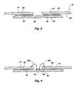
- FIG. 4is a cross sectional depiction of portions of a semiconductor device assembly of the invention with the semiconductor device and the lead frame in contact.
- a semiconductor device assembly 10includes a lead frame 12 having a plurality of lead fingers 14 thereon.
- the lead frame 12is one of a plurality that is connected in end-to-end fashion, thereby forming a strip or roll of lead frames. That is, lead frame 12 is positioned between a preceding frame 16 and a following frame 18 .
- the lead frame 12 as well as the preceding frame 16 and following frame 18are driven or moved through a manufacturing environment by an appropriate drive or indexing system that engages the apertures 20 formed in the opposite edges or rails 22 and 24 .
- the lead frames 12 , 16 and 18are separated one from the other and the opposite edges or rails 22 and 24 are removed so that each frame with a semiconductor device attached thereto becomes a separate and useable semiconductor device assembly.
Landscapes
- Engineering & Computer Science (AREA)
- Computer Hardware Design (AREA)
- Microelectronics & Electronic Packaging (AREA)
- Power Engineering (AREA)
- Physics & Mathematics (AREA)
- Condensed Matter Physics & Semiconductors (AREA)
- General Physics & Mathematics (AREA)
- Manufacturing & Machinery (AREA)
- Die Bonding (AREA)
- Adhesives Or Adhesive Processes (AREA)
Abstract
Description
Claims (12)
Priority Applications (1)
| Application Number | Priority Date | Filing Date | Title |
|---|---|---|---|
| US09/942,140US6653721B2 (en) | 1997-08-14 | 2001-08-29 | LOC semiconductor assembled with room temperature adhesive |
Applications Claiming Priority (4)
| Application Number | Priority Date | Filing Date | Title |
|---|---|---|---|
| US08/916,977US5840598A (en) | 1997-08-14 | 1997-08-14 | LOC semiconductor assembled with room temperature adhesive |
| US09/177,000US5959347A (en) | 1997-08-14 | 1998-10-22 | LOC semiconductor assembled with room temperature adhesive |
| US09/339,718US6316823B1 (en) | 1997-08-14 | 1999-06-24 | LOC semiconductor assembled with room temperature adhesive |
| US09/942,140US6653721B2 (en) | 1997-08-14 | 2001-08-29 | LOC semiconductor assembled with room temperature adhesive |
Related Parent Applications (1)
| Application Number | Title | Priority Date | Filing Date |
|---|---|---|---|
| US09/339,718DivisionUS6316823B1 (en) | 1997-08-14 | 1999-06-24 | LOC semiconductor assembled with room temperature adhesive |
Publications (2)
| Publication Number | Publication Date |
|---|---|
| US20020030253A1 US20020030253A1 (en) | 2002-03-14 |
| US6653721B2true US6653721B2 (en) | 2003-11-25 |
Family
ID=25438175
Family Applications (11)
| Application Number | Title | Priority Date | Filing Date |
|---|---|---|---|
| US08/916,977Expired - LifetimeUS5840598A (en) | 1997-08-14 | 1997-08-14 | LOC semiconductor assembled with room temperature adhesive |
| US09/176,967Expired - LifetimeUS6248611B1 (en) | 1997-08-14 | 1998-10-22 | LOC semiconductor assembled with room temperature adhesive |
| US09/177,000Expired - LifetimeUS5959347A (en) | 1997-08-14 | 1998-10-22 | LOC semiconductor assembled with room temperature adhesive |
| US09/339,718Expired - Fee RelatedUS6316823B1 (en) | 1997-08-14 | 1999-06-24 | LOC semiconductor assembled with room temperature adhesive |
| US09/569,216Expired - LifetimeUS6337511B1 (en) | 1997-08-14 | 2000-05-11 | LOC semiconductor assembled with room temperature adhesive |
| US09/795,889Expired - Fee RelatedUS6391680B2 (en) | 1997-08-14 | 2001-02-28 | LOC semiconductor assembled with room temperature adhesive |
| US09/942,140Expired - LifetimeUS6653721B2 (en) | 1997-08-14 | 2001-08-29 | LOC semiconductor assembled with room temperature adhesive |
| US10/035,078Expired - Fee RelatedUS6979888B2 (en) | 1997-08-14 | 2001-12-28 | LOC semiconductor assembled with room temperature adhesive |
| US10/067,592Expired - LifetimeUS6534342B2 (en) | 1997-08-14 | 2002-02-04 | Method of manufacturing LOC semiconductor assembled with room temperature adhesive |
| US10/389,511Expired - Fee RelatedUS6787396B2 (en) | 1997-08-14 | 2003-03-14 | Method of manufacturing LOC semiconductor assembled with room temperature adhesive |
| US11/237,049AbandonedUS20060022314A1 (en) | 1997-08-14 | 2005-09-27 | LOC semiconductor assembled with room temperature adhesive |
Family Applications Before (6)
| Application Number | Title | Priority Date | Filing Date |
|---|---|---|---|
| US08/916,977Expired - LifetimeUS5840598A (en) | 1997-08-14 | 1997-08-14 | LOC semiconductor assembled with room temperature adhesive |
| US09/176,967Expired - LifetimeUS6248611B1 (en) | 1997-08-14 | 1998-10-22 | LOC semiconductor assembled with room temperature adhesive |
| US09/177,000Expired - LifetimeUS5959347A (en) | 1997-08-14 | 1998-10-22 | LOC semiconductor assembled with room temperature adhesive |
| US09/339,718Expired - Fee RelatedUS6316823B1 (en) | 1997-08-14 | 1999-06-24 | LOC semiconductor assembled with room temperature adhesive |
| US09/569,216Expired - LifetimeUS6337511B1 (en) | 1997-08-14 | 2000-05-11 | LOC semiconductor assembled with room temperature adhesive |
| US09/795,889Expired - Fee RelatedUS6391680B2 (en) | 1997-08-14 | 2001-02-28 | LOC semiconductor assembled with room temperature adhesive |
Family Applications After (4)
| Application Number | Title | Priority Date | Filing Date |
|---|---|---|---|
| US10/035,078Expired - Fee RelatedUS6979888B2 (en) | 1997-08-14 | 2001-12-28 | LOC semiconductor assembled with room temperature adhesive |
| US10/067,592Expired - LifetimeUS6534342B2 (en) | 1997-08-14 | 2002-02-04 | Method of manufacturing LOC semiconductor assembled with room temperature adhesive |
| US10/389,511Expired - Fee RelatedUS6787396B2 (en) | 1997-08-14 | 2003-03-14 | Method of manufacturing LOC semiconductor assembled with room temperature adhesive |
| US11/237,049AbandonedUS20060022314A1 (en) | 1997-08-14 | 2005-09-27 | LOC semiconductor assembled with room temperature adhesive |
Country Status (1)
| Country | Link |
|---|---|
| US (11) | US5840598A (en) |
Families Citing this family (71)
| Publication number | Priority date | Publication date | Assignee | Title |
|---|---|---|---|---|
| US6826827B1 (en)* | 1994-12-29 | 2004-12-07 | Tessera, Inc. | Forming conductive posts by selective removal of conductive material |
| US5810926A (en)* | 1996-03-11 | 1998-09-22 | Micron Technology, Inc. | Method and apparatus for applying atomized adhesive to a leadframe for chip bonding |
| US6030857A (en) | 1996-03-11 | 2000-02-29 | Micron Technology, Inc. | Method for application of spray adhesive to a leadframe for chip bonding |
| US6132798A (en)* | 1998-08-13 | 2000-10-17 | Micron Technology, Inc. | Method for applying atomized adhesive to a leadframe for chip bonding |
| US6017776A (en) | 1997-04-29 | 2000-01-25 | Micron Technology, Inc. | Method of attaching a leadframe to singulated semiconductor dice |
| US6013535A (en)* | 1997-08-05 | 2000-01-11 | Micron Technology, Inc. | Method for applying adhesives to a lead frame |
| US6336973B1 (en) | 1997-08-05 | 2002-01-08 | Micron Technology, Inc. | Apparatus and method for modifying the configuration of an exposed surface of a viscous fluid |
| US6040205A (en)* | 1997-08-05 | 2000-03-21 | Micron Technology, Inc. | Apparatus and method for controlling the depth of immersion of a semiconductor element in an exposed surface of a viscous fluid |
| US5840598A (en)* | 1997-08-14 | 1998-11-24 | Micron Technology, Inc. | LOC semiconductor assembled with room temperature adhesive |
| DE19856833A1 (en)* | 1998-12-09 | 2000-06-21 | Siemens Ag | Method of making an integrated circuit |
| US6291881B1 (en)* | 1999-03-04 | 2001-09-18 | United Microelectronics Corp. | Dual silicon chip package |
| US6359334B1 (en) | 1999-06-08 | 2002-03-19 | Micron Technology, Inc. | Thermally conductive adhesive tape for semiconductor devices and method using the same |
| US7174626B2 (en)* | 1999-06-30 | 2007-02-13 | Intersil Americas, Inc. | Method of manufacturing a plated electronic termination |
| US6774480B1 (en) | 1999-07-30 | 2004-08-10 | Micron Technology, Inc. | Method and structure for manufacturing improved yield semiconductor packaged devices |
| US7049761B2 (en) | 2000-02-11 | 2006-05-23 | Altair Engineering, Inc. | Light tube and power supply circuit |
| TW445558B (en)* | 2000-04-14 | 2001-07-11 | Via Tech Inc | Manufacturing method for cavity-down plastic ball grid array package substrate |
| US6426552B1 (en) | 2000-05-19 | 2002-07-30 | Micron Technology, Inc. | Methods employing hybrid adhesive materials to secure components of semiconductor device assemblies and packages to one another and assemblies and packages including components secured to one another with such hybrid adhesive materials |
| TW497236B (en)* | 2001-08-27 | 2002-08-01 | Chipmos Technologies Inc | A soc packaging process |
| US6501187B1 (en)* | 2001-11-21 | 2002-12-31 | Nai Hua Yeh | Semiconductor package structure having central leads and method for packaging the same |
| US7262074B2 (en)* | 2002-07-08 | 2007-08-28 | Micron Technology, Inc. | Methods of fabricating underfilled, encapsulated semiconductor die assemblies |
| US6934928B2 (en)* | 2002-08-27 | 2005-08-23 | Micron Technology, Inc. | Method and apparatus for designing a pattern on a semiconductor surface |
| US6898779B2 (en)* | 2002-08-28 | 2005-05-24 | Micron Technology, Inc. | Pattern generation on a semiconductor surface |
| US6969914B2 (en)* | 2002-08-29 | 2005-11-29 | Micron Technology, Inc. | Electronic device package |
| TWI267959B (en)* | 2002-11-27 | 2006-12-01 | Siliconware Precision Industries Co Ltd | Semiconductor package with chip-supporting member |
| US7303949B2 (en)* | 2003-10-20 | 2007-12-04 | International Business Machines Corporation | High performance stress-enhanced MOSFETs using Si:C and SiGe epitaxial source/drain and method of manufacture |
| DE10350239A1 (en)* | 2003-10-27 | 2005-06-16 | Infineon Technologies Ag | Semiconductor component with housing plastic material, semiconductor chip and circuit carrier and method for producing the same |
| US7453157B2 (en)* | 2004-06-25 | 2008-11-18 | Tessera, Inc. | Microelectronic packages and methods therefor |
| US7511364B2 (en) | 2004-08-31 | 2009-03-31 | Micron Technology, Inc. | Floating lead finger on a lead frame, lead frame strip, and lead frame assembly including same |
| US7443011B2 (en)* | 2006-02-10 | 2008-10-28 | Marvell International Technology Ltd. | System and method for routing supply voltages or other signals between side-by-side die and a lead frame for system in a package (SIP) devices |
| US8325894B2 (en)* | 2006-08-03 | 2012-12-04 | International Business Machines Corporation | Method, system, and program product for managing conference calls |
| AU2007320024B2 (en) | 2006-10-02 | 2012-11-08 | E. R. Squibb & Sons, L.L.C. | Human antibodies that bind CXCR4 and uses thereof |
| US20080150101A1 (en)* | 2006-12-20 | 2008-06-26 | Tessera, Inc. | Microelectronic packages having improved input/output connections and methods therefor |
| US8699684B2 (en) | 2006-12-20 | 2014-04-15 | International Business Machines Corporation | Method, system, and program product for contacting conference call participants |
| US8105880B2 (en) | 2007-12-05 | 2012-01-31 | Analog Devices, Inc. | Method for attaching a semiconductor die to a leadframe, and a semiconductor device |
| AU2009226028B2 (en)* | 2008-03-21 | 2013-11-14 | Variation Reduction Solutions, Inc. | External system for robotic accuracy enhancement |
| US9137903B2 (en) | 2010-12-21 | 2015-09-15 | Tessera, Inc. | Semiconductor chip assembly and method for making same |
| WO2013100783A1 (en) | 2011-12-29 | 2013-07-04 | Intel Corporation | Method and system for control signalling in a data path module |
| US10331583B2 (en) | 2013-09-26 | 2019-06-25 | Intel Corporation | Executing distributed memory operations using processing elements connected by distributed channels |
| US10402168B2 (en)* | 2016-10-01 | 2019-09-03 | Intel Corporation | Low energy consumption mantissa multiplication for floating point multiply-add operations |
| US10558575B2 (en) | 2016-12-30 | 2020-02-11 | Intel Corporation | Processors, methods, and systems with a configurable spatial accelerator |
| US10572376B2 (en) | 2016-12-30 | 2020-02-25 | Intel Corporation | Memory ordering in acceleration hardware |
| US10474375B2 (en) | 2016-12-30 | 2019-11-12 | Intel Corporation | Runtime address disambiguation in acceleration hardware |
| US10416999B2 (en) | 2016-12-30 | 2019-09-17 | Intel Corporation | Processors, methods, and systems with a configurable spatial accelerator |
| US10515046B2 (en) | 2017-07-01 | 2019-12-24 | Intel Corporation | Processors, methods, and systems with a configurable spatial accelerator |
| US10467183B2 (en) | 2017-07-01 | 2019-11-05 | Intel Corporation | Processors and methods for pipelined runtime services in a spatial array |
| US10515049B1 (en) | 2017-07-01 | 2019-12-24 | Intel Corporation | Memory circuits and methods for distributed memory hazard detection and error recovery |
| US10445451B2 (en) | 2017-07-01 | 2019-10-15 | Intel Corporation | Processors, methods, and systems for a configurable spatial accelerator with performance, correctness, and power reduction features |
| US10387319B2 (en) | 2017-07-01 | 2019-08-20 | Intel Corporation | Processors, methods, and systems for a configurable spatial accelerator with memory system performance, power reduction, and atomics support features |
| US10469397B2 (en) | 2017-07-01 | 2019-11-05 | Intel Corporation | Processors and methods with configurable network-based dataflow operator circuits |
| US10445234B2 (en) | 2017-07-01 | 2019-10-15 | Intel Corporation | Processors, methods, and systems for a configurable spatial accelerator with transactional and replay features |
| US11086816B2 (en) | 2017-09-28 | 2021-08-10 | Intel Corporation | Processors, methods, and systems for debugging a configurable spatial accelerator |
| US10496574B2 (en) | 2017-09-28 | 2019-12-03 | Intel Corporation | Processors, methods, and systems for a memory fence in a configurable spatial accelerator |
| US10380063B2 (en) | 2017-09-30 | 2019-08-13 | Intel Corporation | Processors, methods, and systems with a configurable spatial accelerator having a sequencer dataflow operator |
| US10445098B2 (en) | 2017-09-30 | 2019-10-15 | Intel Corporation | Processors and methods for privileged configuration in a spatial array |
| US10565134B2 (en) | 2017-12-30 | 2020-02-18 | Intel Corporation | Apparatus, methods, and systems for multicast in a configurable spatial accelerator |
| US10445250B2 (en) | 2017-12-30 | 2019-10-15 | Intel Corporation | Apparatus, methods, and systems with a configurable spatial accelerator |
| US10417175B2 (en) | 2017-12-30 | 2019-09-17 | Intel Corporation | Apparatus, methods, and systems for memory consistency in a configurable spatial accelerator |
| US10564980B2 (en) | 2018-04-03 | 2020-02-18 | Intel Corporation | Apparatus, methods, and systems for conditional queues in a configurable spatial accelerator |
| US11307873B2 (en) | 2018-04-03 | 2022-04-19 | Intel Corporation | Apparatus, methods, and systems for unstructured data flow in a configurable spatial accelerator with predicate propagation and merging |
| US10853073B2 (en) | 2018-06-30 | 2020-12-01 | Intel Corporation | Apparatuses, methods, and systems for conditional operations in a configurable spatial accelerator |
| US11200186B2 (en) | 2018-06-30 | 2021-12-14 | Intel Corporation | Apparatuses, methods, and systems for operations in a configurable spatial accelerator |
| US10891240B2 (en) | 2018-06-30 | 2021-01-12 | Intel Corporation | Apparatus, methods, and systems for low latency communication in a configurable spatial accelerator |
| US10459866B1 (en) | 2018-06-30 | 2019-10-29 | Intel Corporation | Apparatuses, methods, and systems for integrated control and data processing in a configurable spatial accelerator |
| US10678724B1 (en) | 2018-12-29 | 2020-06-09 | Intel Corporation | Apparatuses, methods, and systems for in-network storage in a configurable spatial accelerator |
| US11029927B2 (en) | 2019-03-30 | 2021-06-08 | Intel Corporation | Methods and apparatus to detect and annotate backedges in a dataflow graph |
| US10965536B2 (en) | 2019-03-30 | 2021-03-30 | Intel Corporation | Methods and apparatus to insert buffers in a dataflow graph |
| US10915471B2 (en) | 2019-03-30 | 2021-02-09 | Intel Corporation | Apparatuses, methods, and systems for memory interface circuit allocation in a configurable spatial accelerator |
| US10817291B2 (en) | 2019-03-30 | 2020-10-27 | Intel Corporation | Apparatuses, methods, and systems for swizzle operations in a configurable spatial accelerator |
| US11037050B2 (en) | 2019-06-29 | 2021-06-15 | Intel Corporation | Apparatuses, methods, and systems for memory interface circuit arbitration in a configurable spatial accelerator |
| US11907713B2 (en) | 2019-12-28 | 2024-02-20 | Intel Corporation | Apparatuses, methods, and systems for fused operations using sign modification in a processing element of a configurable spatial accelerator |
| US12086080B2 (en) | 2020-09-26 | 2024-09-10 | Intel Corporation | Apparatuses, methods, and systems for a configurable accelerator having dataflow execution circuits |
Citations (22)
| Publication number | Priority date | Publication date | Assignee | Title |
|---|---|---|---|---|
| US4934820A (en) | 1987-10-20 | 1990-06-19 | Hitachi, Ltd. | Semiconductor device |
| US4937656A (en) | 1988-04-22 | 1990-06-26 | Mitsubishi Denki Kabushiki Kaisha | Semiconductor device |
| US5073521A (en) | 1989-11-15 | 1991-12-17 | Olin Corporation | Method for housing a tape-bonded electronic device and the package employed |
| US5256598A (en) | 1992-04-15 | 1993-10-26 | Micron Technology, Inc. | Shrink accommodating lead frame |
| US5286679A (en) | 1993-03-18 | 1994-02-15 | Micron Technology, Inc. | Method for attaching a semiconductor die to a leadframe using a patterned adhesive layer |
| US5304842A (en) | 1990-10-24 | 1994-04-19 | Micron Technology, Inc. | Dissimilar adhesive die attach for semiconductor devices |
| US5304582A (en)* | 1988-04-28 | 1994-04-19 | Matsushita Electric Industrial Co., Ltd. | Process for producing polyacetylene or polyacene type long conjugated polymers |
| US5350811A (en) | 1990-04-20 | 1994-09-27 | Hitachi Chemical Co. Ltd. | Epoxy resin and adhesive composition containing the same |
| US5366933A (en) | 1993-10-13 | 1994-11-22 | Intel Corporation | Method for constructing a dual sided, wire bonded integrated circuit chip package |
| US5407502A (en) | 1989-12-19 | 1995-04-18 | Fujitsu Limited | Method for producing a semiconductor device having an improved adhesive structure |
| US5441918A (en) | 1993-01-29 | 1995-08-15 | Lsi Logic Corporation | Method of making integrated circuit die package |
| US5446080A (en) | 1993-10-29 | 1995-08-29 | Tomoegawa Paper Co., Ltd. | Liquid adhesive for electronic parts and process for forming insulating adhesive layer using the same |
| US5506446A (en) | 1994-04-14 | 1996-04-09 | Olin Corporation | Electronic package having improved wire bonding capability |
| US5548160A (en)* | 1994-11-14 | 1996-08-20 | Micron Technology, Inc. | Method and structure for attaching a semiconductor die to a lead frame |
| US5627108A (en) | 1995-06-21 | 1997-05-06 | Compaq Computer Corporation | Solder paste and glue dot-based methods of securing components to a printed circuit board |
| US5755867A (en) | 1995-12-22 | 1998-05-26 | Shin-Etsu Chemical Co., Ltd. | Photocatalytic hydrophilic coating compositions |
| US5840598A (en) | 1997-08-14 | 1998-11-24 | Micron Technology, Inc. | LOC semiconductor assembled with room temperature adhesive |
| US5863988A (en) | 1995-12-25 | 1999-01-26 | Tomoegawa Paper Co., Ltd. | Liquid adhesive for electronic parts and adhesive tape |
| US5872398A (en) | 1996-01-11 | 1999-02-16 | Micron Technology, Inc. | Reduced stress LOC assembly including cantilevered leads |
| US5982041A (en) | 1996-04-19 | 1999-11-09 | Dow Corning Toray Silicone Co., Ltd. | Silicone die attach adhesive, method for the fabrication of semiconductor devices, and semiconductor devices |
| US6011220A (en) | 1995-11-16 | 2000-01-04 | Kabushiki Kaisha Toshiba | Semiconductor packaged device and lead frame used therein |
| US6012502A (en) | 1995-07-31 | 2000-01-11 | Micron Technology, Inc. | Apparatus for attaching adhesive tape to lead-on-chip leadframes |
Family Cites Families (8)
| Publication number | Priority date | Publication date | Assignee | Title |
|---|---|---|---|---|
| US4763659A (en)* | 1985-08-21 | 1988-08-16 | Spring Creek Institute, Inc. | Dry electrode system for detection of biopotentials |
| US4740584A (en)* | 1986-09-08 | 1988-04-26 | Interez, Inc. | Blend of dicyanate esters of dihydric phenols |
| US5162574A (en)* | 1986-11-24 | 1992-11-10 | Hi-Tek Polymers, Inc. | Bis(4-cyanatophenyl)-1,1-ethane |
| AU597435B2 (en)* | 1986-11-24 | 1990-05-31 | Ciba-Geigy Ag | Low viscosity noncrystalline dicyanate esters and blends with prepolymers of dicyanate esters |
| US5336933A (en)* | 1990-07-16 | 1994-08-09 | Bru-Mel Corporation | Fluid-augmented free-vortex power generating apparatus |
| US6359335B1 (en)* | 1994-05-19 | 2002-03-19 | Tessera, Inc. | Method of manufacturing a plurality of semiconductor packages and the resulting semiconductor package structures |
| US6214640B1 (en)* | 1999-02-10 | 2001-04-10 | Tessera, Inc. | Method of manufacturing a plurality of semiconductor packages |
| US6232366B1 (en)* | 1999-06-09 | 2001-05-15 | 3M Innovative Properties Company | Pressure sensitive conductive adhesive having hot-melt properties and biomedical electrodes using same |
- 1997
- 1997-08-14USUS08/916,977patent/US5840598A/ennot_activeExpired - Lifetime
- 1998
- 1998-10-22USUS09/176,967patent/US6248611B1/ennot_activeExpired - Lifetime
- 1998-10-22USUS09/177,000patent/US5959347A/ennot_activeExpired - Lifetime
- 1999
- 1999-06-24USUS09/339,718patent/US6316823B1/ennot_activeExpired - Fee Related
- 2000
- 2000-05-11USUS09/569,216patent/US6337511B1/ennot_activeExpired - Lifetime
- 2001
- 2001-02-28USUS09/795,889patent/US6391680B2/ennot_activeExpired - Fee Related
- 2001-08-29USUS09/942,140patent/US6653721B2/ennot_activeExpired - Lifetime
- 2001-12-28USUS10/035,078patent/US6979888B2/ennot_activeExpired - Fee Related
- 2002
- 2002-02-04USUS10/067,592patent/US6534342B2/ennot_activeExpired - Lifetime
- 2003
- 2003-03-14USUS10/389,511patent/US6787396B2/ennot_activeExpired - Fee Related
- 2005
- 2005-09-27USUS11/237,049patent/US20060022314A1/ennot_activeAbandoned
Patent Citations (23)
| Publication number | Priority date | Publication date | Assignee | Title |
|---|---|---|---|---|
| US4934820A (en) | 1987-10-20 | 1990-06-19 | Hitachi, Ltd. | Semiconductor device |
| US4937656A (en) | 1988-04-22 | 1990-06-26 | Mitsubishi Denki Kabushiki Kaisha | Semiconductor device |
| US5304582A (en)* | 1988-04-28 | 1994-04-19 | Matsushita Electric Industrial Co., Ltd. | Process for producing polyacetylene or polyacene type long conjugated polymers |
| US5073521A (en) | 1989-11-15 | 1991-12-17 | Olin Corporation | Method for housing a tape-bonded electronic device and the package employed |
| US5407502A (en) | 1989-12-19 | 1995-04-18 | Fujitsu Limited | Method for producing a semiconductor device having an improved adhesive structure |
| US5350811A (en) | 1990-04-20 | 1994-09-27 | Hitachi Chemical Co. Ltd. | Epoxy resin and adhesive composition containing the same |
| US5304842A (en) | 1990-10-24 | 1994-04-19 | Micron Technology, Inc. | Dissimilar adhesive die attach for semiconductor devices |
| US5256598A (en) | 1992-04-15 | 1993-10-26 | Micron Technology, Inc. | Shrink accommodating lead frame |
| US5441918A (en) | 1993-01-29 | 1995-08-15 | Lsi Logic Corporation | Method of making integrated circuit die package |
| US5286679A (en) | 1993-03-18 | 1994-02-15 | Micron Technology, Inc. | Method for attaching a semiconductor die to a leadframe using a patterned adhesive layer |
| US5366933A (en) | 1993-10-13 | 1994-11-22 | Intel Corporation | Method for constructing a dual sided, wire bonded integrated circuit chip package |
| US5446080A (en) | 1993-10-29 | 1995-08-29 | Tomoegawa Paper Co., Ltd. | Liquid adhesive for electronic parts and process for forming insulating adhesive layer using the same |
| US5506446A (en) | 1994-04-14 | 1996-04-09 | Olin Corporation | Electronic package having improved wire bonding capability |
| US5548160A (en)* | 1994-11-14 | 1996-08-20 | Micron Technology, Inc. | Method and structure for attaching a semiconductor die to a lead frame |
| US5627108A (en) | 1995-06-21 | 1997-05-06 | Compaq Computer Corporation | Solder paste and glue dot-based methods of securing components to a printed circuit board |
| US6012502A (en) | 1995-07-31 | 2000-01-11 | Micron Technology, Inc. | Apparatus for attaching adhesive tape to lead-on-chip leadframes |
| US6011220A (en) | 1995-11-16 | 2000-01-04 | Kabushiki Kaisha Toshiba | Semiconductor packaged device and lead frame used therein |
| US5755867A (en) | 1995-12-22 | 1998-05-26 | Shin-Etsu Chemical Co., Ltd. | Photocatalytic hydrophilic coating compositions |
| US5863988A (en) | 1995-12-25 | 1999-01-26 | Tomoegawa Paper Co., Ltd. | Liquid adhesive for electronic parts and adhesive tape |
| US5872398A (en) | 1996-01-11 | 1999-02-16 | Micron Technology, Inc. | Reduced stress LOC assembly including cantilevered leads |
| US5982041A (en) | 1996-04-19 | 1999-11-09 | Dow Corning Toray Silicone Co., Ltd. | Silicone die attach adhesive, method for the fabrication of semiconductor devices, and semiconductor devices |
| US5959347A (en) | 1997-08-14 | 1999-09-28 | Micron Technology, Inc. | LOC semiconductor assembled with room temperature adhesive |
| US5840598A (en) | 1997-08-14 | 1998-11-24 | Micron Technology, Inc. | LOC semiconductor assembled with room temperature adhesive |
Also Published As
| Publication number | Publication date |
|---|---|
| US6316823B1 (en) | 2001-11-13 |
| US20030176019A1 (en) | 2003-09-18 |
| US6979888B2 (en) | 2005-12-27 |
| US20020090751A1 (en) | 2002-07-11 |
| US20060022314A1 (en) | 2006-02-02 |
| US20020030253A1 (en) | 2002-03-14 |
| US6787396B2 (en) | 2004-09-07 |
| US6337511B1 (en) | 2002-01-08 |
| US6534342B2 (en) | 2003-03-18 |
| US5959347A (en) | 1999-09-28 |
| US6248611B1 (en) | 2001-06-19 |
| US6391680B2 (en) | 2002-05-21 |
| US20020056896A1 (en) | 2002-05-16 |
| US20010007784A1 (en) | 2001-07-12 |
| US5840598A (en) | 1998-11-24 |
Similar Documents
| Publication | Publication Date | Title |
|---|---|---|
| US6653721B2 (en) | LOC semiconductor assembled with room temperature adhesive | |
| US7071078B2 (en) | Methods for securing components of semiconductor device assemblies to each other with hybrid adhesive materials | |
| US6706559B2 (en) | Method of attaching a leadframe to singulated semiconductor dice | |
| JP2000332055A (en) | Flip-chip mounting structure and mounting method | |
| US6528867B1 (en) | Integrated circuit devices including connection components mechanically and electrically attached to semiconductor dice | |
| JPH11121543A (en) | Chip scale package | |
| EP0844656A1 (en) | Electronic component structure | |
| US5933708A (en) | Lead-on-chip semiconductor package and method for making the same | |
| US6107118A (en) | Chip-contacting method requiring no contact bumps, and electronic circuit produced in this way | |
| JPS623978B2 (en) | ||
| KR100219348B1 (en) | Chip paste method using paste | |
| JP2542675B2 (en) | Semiconductor device | |
| US6407457B1 (en) | Contact-bumpless chip contacting method and an electronic circuit produced by said method | |
| JP3287233B2 (en) | Method for manufacturing semiconductor device | |
| JP2789827B2 (en) | Semiconductor device | |
| JP2000216172A (en) | Manufacturing apparatus of semiconductor device | |
| JPH07226412A (en) | Method for manufacturing semiconductor device | |
| JPH1098069A (en) | Projection electrode of semiconductor device and liquid crystal display device | |
| JPH11135531A (en) | Semiconductor device and mounting method thereof | |
| JPH1032286A (en) | Semiconductor device | |
| JPH0418790A (en) | Electronic device mounting method | |
| JPH01241836A (en) | How to connect leads of IC parts |
Legal Events
| Date | Code | Title | Description |
|---|---|---|---|
| STCF | Information on status: patent grant | Free format text:PATENTED CASE | |
| FEPP | Fee payment procedure | Free format text:PAYOR NUMBER ASSIGNED (ORIGINAL EVENT CODE: ASPN); ENTITY STATUS OF PATENT OWNER: LARGE ENTITY | |
| CC | Certificate of correction | ||
| FPAY | Fee payment | Year of fee payment:4 | |
| FPAY | Fee payment | Year of fee payment:8 | |
| FPAY | Fee payment | Year of fee payment:12 | |
| AS | Assignment | Owner name:U.S. BANK NATIONAL ASSOCIATION, AS COLLATERAL AGENT, CALIFORNIA Free format text:SECURITY INTEREST;ASSIGNOR:MICRON TECHNOLOGY, INC.;REEL/FRAME:038669/0001 Effective date:20160426 Owner name:U.S. BANK NATIONAL ASSOCIATION, AS COLLATERAL AGEN Free format text:SECURITY INTEREST;ASSIGNOR:MICRON TECHNOLOGY, INC.;REEL/FRAME:038669/0001 Effective date:20160426 | |
| AS | Assignment | Owner name:MORGAN STANLEY SENIOR FUNDING, INC., AS COLLATERAL AGENT, MARYLAND Free format text:PATENT SECURITY AGREEMENT;ASSIGNOR:MICRON TECHNOLOGY, INC.;REEL/FRAME:038954/0001 Effective date:20160426 Owner name:MORGAN STANLEY SENIOR FUNDING, INC., AS COLLATERAL Free format text:PATENT SECURITY AGREEMENT;ASSIGNOR:MICRON TECHNOLOGY, INC.;REEL/FRAME:038954/0001 Effective date:20160426 | |
| AS | Assignment | Owner name:U.S. BANK NATIONAL ASSOCIATION, AS COLLATERAL AGENT, CALIFORNIA Free format text:CORRECTIVE ASSIGNMENT TO CORRECT THE REPLACE ERRONEOUSLY FILED PATENT #7358718 WITH THE CORRECT PATENT #7358178 PREVIOUSLY RECORDED ON REEL 038669 FRAME 0001. ASSIGNOR(S) HEREBY CONFIRMS THE SECURITY INTEREST;ASSIGNOR:MICRON TECHNOLOGY, INC.;REEL/FRAME:043079/0001 Effective date:20160426 Owner name:U.S. BANK NATIONAL ASSOCIATION, AS COLLATERAL AGEN Free format text:CORRECTIVE ASSIGNMENT TO CORRECT THE REPLACE ERRONEOUSLY FILED PATENT #7358718 WITH THE CORRECT PATENT #7358178 PREVIOUSLY RECORDED ON REEL 038669 FRAME 0001. ASSIGNOR(S) HEREBY CONFIRMS THE SECURITY INTEREST;ASSIGNOR:MICRON TECHNOLOGY, INC.;REEL/FRAME:043079/0001 Effective date:20160426 | |
| AS | Assignment | Owner name:MICRON TECHNOLOGY, INC., IDAHO Free format text:RELEASE BY SECURED PARTY;ASSIGNOR:U.S. BANK NATIONAL ASSOCIATION, AS COLLATERAL AGENT;REEL/FRAME:047243/0001 Effective date:20180629 | |
| AS | Assignment | Owner name:MICRON TECHNOLOGY, INC., IDAHO Free format text:RELEASE BY SECURED PARTY;ASSIGNOR:MORGAN STANLEY SENIOR FUNDING, INC., AS COLLATERAL AGENT;REEL/FRAME:050937/0001 Effective date:20190731 |