US6653563B2 - Alternate bump metallurgy bars for power and ground routing - Google Patents
Alternate bump metallurgy bars for power and ground routingDownload PDFInfo
- Publication number
- US6653563B2 US6653563B2US09/823,427US82342701AUS6653563B2US 6653563 B2US6653563 B2US 6653563B2US 82342701 AUS82342701 AUS 82342701AUS 6653563 B2US6653563 B2US 6653563B2
- Authority
- US
- United States
- Prior art keywords
- power
- die
- ground
- bars
- passivation
- Prior art date
- Legal status (The legal status is an assumption and is not a legal conclusion. Google has not performed a legal analysis and makes no representation as to the accuracy of the status listed.)
- Expired - Lifetime, expires
Links
Images


Classifications
- H—ELECTRICITY
- H01—ELECTRIC ELEMENTS
- H01L—SEMICONDUCTOR DEVICES NOT COVERED BY CLASS H10
- H01L24/00—Arrangements for connecting or disconnecting semiconductor or solid-state bodies; Methods or apparatus related thereto
- H01L24/01—Means for bonding being attached to, or being formed on, the surface to be connected, e.g. chip-to-package, die-attach, "first-level" interconnects; Manufacturing methods related thereto
- H01L24/10—Bump connectors ; Manufacturing methods related thereto
- H—ELECTRICITY
- H01—ELECTRIC ELEMENTS
- H01L—SEMICONDUCTOR DEVICES NOT COVERED BY CLASS H10
- H01L23/00—Details of semiconductor or other solid state devices
- H01L23/48—Arrangements for conducting electric current to or from the solid state body in operation, e.g. leads, terminal arrangements ; Selection of materials therefor
- H01L23/50—Arrangements for conducting electric current to or from the solid state body in operation, e.g. leads, terminal arrangements ; Selection of materials therefor for integrated circuit devices, e.g. power bus, number of leads
- H—ELECTRICITY
- H01—ELECTRIC ELEMENTS
- H01L—SEMICONDUCTOR DEVICES NOT COVERED BY CLASS H10
- H01L23/00—Details of semiconductor or other solid state devices
- H01L23/52—Arrangements for conducting electric current within the device in operation from one component to another, i.e. interconnections, e.g. wires, lead frames
- H01L23/522—Arrangements for conducting electric current within the device in operation from one component to another, i.e. interconnections, e.g. wires, lead frames including external interconnections consisting of a multilayer structure of conductive and insulating layers inseparably formed on the semiconductor body
- H01L23/528—Layout of the interconnection structure
- H01L23/5286—Arrangements of power or ground buses
- H—ELECTRICITY
- H01—ELECTRIC ELEMENTS
- H01L—SEMICONDUCTOR DEVICES NOT COVERED BY CLASS H10
- H01L24/00—Arrangements for connecting or disconnecting semiconductor or solid-state bodies; Methods or apparatus related thereto
- H01L24/01—Means for bonding being attached to, or being formed on, the surface to be connected, e.g. chip-to-package, die-attach, "first-level" interconnects; Manufacturing methods related thereto
- H01L24/10—Bump connectors ; Manufacturing methods related thereto
- H01L24/12—Structure, shape, material or disposition of the bump connectors prior to the connecting process
- H01L24/13—Structure, shape, material or disposition of the bump connectors prior to the connecting process of an individual bump connector
- H—ELECTRICITY
- H01—ELECTRIC ELEMENTS
- H01L—SEMICONDUCTOR DEVICES NOT COVERED BY CLASS H10
- H01L24/00—Arrangements for connecting or disconnecting semiconductor or solid-state bodies; Methods or apparatus related thereto
- H01L24/01—Means for bonding being attached to, or being formed on, the surface to be connected, e.g. chip-to-package, die-attach, "first-level" interconnects; Manufacturing methods related thereto
- H01L24/10—Bump connectors ; Manufacturing methods related thereto
- H01L24/12—Structure, shape, material or disposition of the bump connectors prior to the connecting process
- H01L24/14—Structure, shape, material or disposition of the bump connectors prior to the connecting process of a plurality of bump connectors
- H—ELECTRICITY
- H01—ELECTRIC ELEMENTS
- H01L—SEMICONDUCTOR DEVICES NOT COVERED BY CLASS H10
- H01L2224/00—Indexing scheme for arrangements for connecting or disconnecting semiconductor or solid-state bodies and methods related thereto as covered by H01L24/00
- H01L2224/01—Means for bonding being attached to, or being formed on, the surface to be connected, e.g. chip-to-package, die-attach, "first-level" interconnects; Manufacturing methods related thereto
- H01L2224/10—Bump connectors; Manufacturing methods related thereto
- H01L2224/12—Structure, shape, material or disposition of the bump connectors prior to the connecting process
- H01L2224/13—Structure, shape, material or disposition of the bump connectors prior to the connecting process of an individual bump connector
- H01L2224/13001—Core members of the bump connector
- H01L2224/13099—Material
- H—ELECTRICITY
- H01—ELECTRIC ELEMENTS
- H01L—SEMICONDUCTOR DEVICES NOT COVERED BY CLASS H10
- H01L2224/00—Indexing scheme for arrangements for connecting or disconnecting semiconductor or solid-state bodies and methods related thereto as covered by H01L24/00
- H01L2224/01—Means for bonding being attached to, or being formed on, the surface to be connected, e.g. chip-to-package, die-attach, "first-level" interconnects; Manufacturing methods related thereto
- H01L2224/10—Bump connectors; Manufacturing methods related thereto
- H01L2224/12—Structure, shape, material or disposition of the bump connectors prior to the connecting process
- H01L2224/14—Structure, shape, material or disposition of the bump connectors prior to the connecting process of a plurality of bump connectors
- H01L2224/1405—Shape
- H01L2224/14051—Bump connectors having different shapes
- H—ELECTRICITY
- H01—ELECTRIC ELEMENTS
- H01L—SEMICONDUCTOR DEVICES NOT COVERED BY CLASS H10
- H01L2224/00—Indexing scheme for arrangements for connecting or disconnecting semiconductor or solid-state bodies and methods related thereto as covered by H01L24/00
- H01L2224/01—Means for bonding being attached to, or being formed on, the surface to be connected, e.g. chip-to-package, die-attach, "first-level" interconnects; Manufacturing methods related thereto
- H01L2224/10—Bump connectors; Manufacturing methods related thereto
- H01L2224/12—Structure, shape, material or disposition of the bump connectors prior to the connecting process
- H01L2224/14—Structure, shape, material or disposition of the bump connectors prior to the connecting process of a plurality of bump connectors
- H01L2224/141—Disposition
- H01L2224/1412—Layout
- H01L2224/1413—Square or rectangular array
- H01L2224/14133—Square or rectangular array with a staggered arrangement, e.g. depopulated array
- H—ELECTRICITY
- H01—ELECTRIC ELEMENTS
- H01L—SEMICONDUCTOR DEVICES NOT COVERED BY CLASS H10
- H01L2224/00—Indexing scheme for arrangements for connecting or disconnecting semiconductor or solid-state bodies and methods related thereto as covered by H01L24/00
- H01L2224/01—Means for bonding being attached to, or being formed on, the surface to be connected, e.g. chip-to-package, die-attach, "first-level" interconnects; Manufacturing methods related thereto
- H01L2224/10—Bump connectors; Manufacturing methods related thereto
- H01L2224/15—Structure, shape, material or disposition of the bump connectors after the connecting process
- H01L2224/16—Structure, shape, material or disposition of the bump connectors after the connecting process of an individual bump connector
- H—ELECTRICITY
- H01—ELECTRIC ELEMENTS
- H01L—SEMICONDUCTOR DEVICES NOT COVERED BY CLASS H10
- H01L2924/00—Indexing scheme for arrangements or methods for connecting or disconnecting semiconductor or solid-state bodies as covered by H01L24/00
- H01L2924/0001—Technical content checked by a classifier
- H01L2924/00014—Technical content checked by a classifier the subject-matter covered by the group, the symbol of which is combined with the symbol of this group, being disclosed without further technical details
- H—ELECTRICITY
- H01—ELECTRIC ELEMENTS
- H01L—SEMICONDUCTOR DEVICES NOT COVERED BY CLASS H10
- H01L2924/00—Indexing scheme for arrangements or methods for connecting or disconnecting semiconductor or solid-state bodies as covered by H01L24/00
- H01L2924/01—Chemical elements
- H01L2924/01005—Boron [B]
- H—ELECTRICITY
- H01—ELECTRIC ELEMENTS
- H01L—SEMICONDUCTOR DEVICES NOT COVERED BY CLASS H10
- H01L2924/00—Indexing scheme for arrangements or methods for connecting or disconnecting semiconductor or solid-state bodies as covered by H01L24/00
- H01L2924/01—Chemical elements
- H01L2924/01006—Carbon [C]
- H—ELECTRICITY
- H01—ELECTRIC ELEMENTS
- H01L—SEMICONDUCTOR DEVICES NOT COVERED BY CLASS H10
- H01L2924/00—Indexing scheme for arrangements or methods for connecting or disconnecting semiconductor or solid-state bodies as covered by H01L24/00
- H01L2924/01—Chemical elements
- H01L2924/01013—Aluminum [Al]
- H—ELECTRICITY
- H01—ELECTRIC ELEMENTS
- H01L—SEMICONDUCTOR DEVICES NOT COVERED BY CLASS H10
- H01L2924/00—Indexing scheme for arrangements or methods for connecting or disconnecting semiconductor or solid-state bodies as covered by H01L24/00
- H01L2924/01—Chemical elements
- H01L2924/01015—Phosphorus [P]
- H—ELECTRICITY
- H01—ELECTRIC ELEMENTS
- H01L—SEMICONDUCTOR DEVICES NOT COVERED BY CLASS H10
- H01L2924/00—Indexing scheme for arrangements or methods for connecting or disconnecting semiconductor or solid-state bodies as covered by H01L24/00
- H01L2924/01—Chemical elements
- H01L2924/01019—Potassium [K]
- H—ELECTRICITY
- H01—ELECTRIC ELEMENTS
- H01L—SEMICONDUCTOR DEVICES NOT COVERED BY CLASS H10
- H01L2924/00—Indexing scheme for arrangements or methods for connecting or disconnecting semiconductor or solid-state bodies as covered by H01L24/00
- H01L2924/01—Chemical elements
- H01L2924/01022—Titanium [Ti]
- H—ELECTRICITY
- H01—ELECTRIC ELEMENTS
- H01L—SEMICONDUCTOR DEVICES NOT COVERED BY CLASS H10
- H01L2924/00—Indexing scheme for arrangements or methods for connecting or disconnecting semiconductor or solid-state bodies as covered by H01L24/00
- H01L2924/01—Chemical elements
- H01L2924/01023—Vanadium [V]
- H—ELECTRICITY
- H01—ELECTRIC ELEMENTS
- H01L—SEMICONDUCTOR DEVICES NOT COVERED BY CLASS H10
- H01L2924/00—Indexing scheme for arrangements or methods for connecting or disconnecting semiconductor or solid-state bodies as covered by H01L24/00
- H01L2924/01—Chemical elements
- H01L2924/01029—Copper [Cu]
- H—ELECTRICITY
- H01—ELECTRIC ELEMENTS
- H01L—SEMICONDUCTOR DEVICES NOT COVERED BY CLASS H10
- H01L2924/00—Indexing scheme for arrangements or methods for connecting or disconnecting semiconductor or solid-state bodies as covered by H01L24/00
- H01L2924/01—Chemical elements
- H01L2924/01033—Arsenic [As]
- H—ELECTRICITY
- H01—ELECTRIC ELEMENTS
- H01L—SEMICONDUCTOR DEVICES NOT COVERED BY CLASS H10
- H01L2924/00—Indexing scheme for arrangements or methods for connecting or disconnecting semiconductor or solid-state bodies as covered by H01L24/00
- H01L2924/01—Chemical elements
- H01L2924/01039—Yttrium [Y]
- H—ELECTRICITY
- H01—ELECTRIC ELEMENTS
- H01L—SEMICONDUCTOR DEVICES NOT COVERED BY CLASS H10
- H01L2924/00—Indexing scheme for arrangements or methods for connecting or disconnecting semiconductor or solid-state bodies as covered by H01L24/00
- H01L2924/01—Chemical elements
- H01L2924/01047—Silver [Ag]
- H—ELECTRICITY
- H01—ELECTRIC ELEMENTS
- H01L—SEMICONDUCTOR DEVICES NOT COVERED BY CLASS H10
- H01L2924/00—Indexing scheme for arrangements or methods for connecting or disconnecting semiconductor or solid-state bodies as covered by H01L24/00
- H01L2924/01—Chemical elements
- H01L2924/01057—Lanthanum [La]
- H—ELECTRICITY
- H01—ELECTRIC ELEMENTS
- H01L—SEMICONDUCTOR DEVICES NOT COVERED BY CLASS H10
- H01L2924/00—Indexing scheme for arrangements or methods for connecting or disconnecting semiconductor or solid-state bodies as covered by H01L24/00
- H01L2924/01—Chemical elements
- H01L2924/01067—Holmium [Ho]
- H—ELECTRICITY
- H01—ELECTRIC ELEMENTS
- H01L—SEMICONDUCTOR DEVICES NOT COVERED BY CLASS H10
- H01L2924/00—Indexing scheme for arrangements or methods for connecting or disconnecting semiconductor or solid-state bodies as covered by H01L24/00
- H01L2924/01—Chemical elements
- H01L2924/01074—Tungsten [W]
- H—ELECTRICITY
- H01—ELECTRIC ELEMENTS
- H01L—SEMICONDUCTOR DEVICES NOT COVERED BY CLASS H10
- H01L2924/00—Indexing scheme for arrangements or methods for connecting or disconnecting semiconductor or solid-state bodies as covered by H01L24/00
- H01L2924/01—Chemical elements
- H01L2924/01078—Platinum [Pt]
- H—ELECTRICITY
- H01—ELECTRIC ELEMENTS
- H01L—SEMICONDUCTOR DEVICES NOT COVERED BY CLASS H10
- H01L2924/00—Indexing scheme for arrangements or methods for connecting or disconnecting semiconductor or solid-state bodies as covered by H01L24/00
- H01L2924/01—Chemical elements
- H01L2924/01082—Lead [Pb]
- H—ELECTRICITY
- H01—ELECTRIC ELEMENTS
- H01L—SEMICONDUCTOR DEVICES NOT COVERED BY CLASS H10
- H01L2924/00—Indexing scheme for arrangements or methods for connecting or disconnecting semiconductor or solid-state bodies as covered by H01L24/00
- H01L2924/013—Alloys
- H01L2924/014—Solder alloys
- H—ELECTRICITY
- H01—ELECTRIC ELEMENTS
- H01L—SEMICONDUCTOR DEVICES NOT COVERED BY CLASS H10
- H01L2924/00—Indexing scheme for arrangements or methods for connecting or disconnecting semiconductor or solid-state bodies as covered by H01L24/00
- H01L2924/10—Details of semiconductor or other solid state devices to be connected
- H01L2924/11—Device type
- H01L2924/14—Integrated circuits
- H—ELECTRICITY
- H01—ELECTRIC ELEMENTS
- H01L—SEMICONDUCTOR DEVICES NOT COVERED BY CLASS H10
- H01L2924/00—Indexing scheme for arrangements or methods for connecting or disconnecting semiconductor or solid-state bodies as covered by H01L24/00
- H01L2924/15—Details of package parts other than the semiconductor or other solid state devices to be connected
- H01L2924/151—Die mounting substrate
- H01L2924/153—Connection portion
- H01L2924/1531—Connection portion the connection portion being formed only on the surface of the substrate opposite to the die mounting surface
- H01L2924/15311—Connection portion the connection portion being formed only on the surface of the substrate opposite to the die mounting surface being a ball array, e.g. BGA
- H—ELECTRICITY
- H01—ELECTRIC ELEMENTS
- H01L—SEMICONDUCTOR DEVICES NOT COVERED BY CLASS H10
- H01L2924/00—Indexing scheme for arrangements or methods for connecting or disconnecting semiconductor or solid-state bodies as covered by H01L24/00
- H01L2924/30—Technical effects
- H01L2924/301—Electrical effects
- H01L2924/30107—Inductance
Definitions
- This inventionrelates to the field of microchip packaging and in particular to routing power and ground connections between the microchip and the package substrate.
- FIG. 1Ais an illustration of a die surface with a C4 bump pattern containing I/O for signal, power, and ground. Challenges to provide finer pitch bumps between a die and a die package have increased routing and routing complexity at the die surface.
- FIG. 1Ais an illustration of a die surface with a C4 bump pattern containing I/O for signal, power, and ground. Challenges to provide finer pitch bumps between a die and a die package have increased routing and routing complexity at the die surface.
- 1Bis an illustration of a die surface with ABM bumps connected to ground (Vss) and power (Vdd) lines on the chip.
- Vssground
- Vddpower
- An apparatuscomprising: a die having a surface, comprising: an array of electrically conductive bumps; and a plurality of electrically conductive bars positioned within the array of electrically conductive bumps.
- FIG. 1Ais an illustration of a die surface with a C4 bump pattern containing I/O for signal, power, and ground.
- FIG. 1Bis an illustration of a die surface with ABM bumps connected to ground (Vss) and power (Vdd) lines on the die.
- FIG. 2Ais an illustration of the die with power and ground bars using alternate bump metallurgy.
- FIG. 2Bis an illustration of the die with power and ground bars and an edge ring.
- FIG. 3is an illustration of ABM bars placed over ground and power lines existing within a metal layer and interconnected with lines passivation openings.
- FIG. 4Ais an illustration of the ABM bar connected to the M7 copper layer.
- FIG. 4Bis an illustration of the ABM bar connected to the M7 copper layer in a view rotated 90 degrees from that of FIG. 4 A.
- FIGS. 5A-5Hare illustrations of a method to produce ABM bars on the die.
- FIG. 5Ais an illustration of the die containing power and ground lines within a metal layer.
- FIG. 5Bis an illustration of the die have a dielectric layer deposited over the metal layer.
- FIG. 5Cis an illustration of the die having a passivation layer deposited over the dielectric layer.
- FIG. 5Dis an illustration of the die having passivation openings etched through the dielectric layer and the passivation layer.
- FIG. 5Eis an illustration of the die having lined passivation openings.
- FIG. 5Fis an illustration of the die having a patterned photoresist layer.
- FIG. 5Gis an illustration of the die having the patterns filled in with copper.
- FIG. 5His an illustration of the die with power bars, ground bars, and a bump having alternate bump metallurgy.
- FIGS. 6A and 6Billustrate a die-substrate assembly 600 .
- a structure and method for providing power and ground bars, centered within an array of I/O signal bumps on a die surfaceis disclosed.
- the I/O signal bumps and the power and ground barscould be in the form of copper bumps.
- the structure and methodcan provide an efficient means of connecting power and ground between a microchip (die) and a substrate.
- the structure and methodcan make use of a bump metallurgy that is different from solder (i.e. alternate bump metallurgy or ABM).
- the power and ground structurescan be located on the die with the I/O signal bumps (signal bumps), positioned in an ordered array, surrounding the power and ground structures.
- a structure and method for providing power and ground bars, centered within an array of I/O signal bumps on a die surfaceis disclosed.
- the I/O signal bumps and the power and ground barscould be in the form of copper bumps.
- the structure and methodcan provide an efficient means of connecting power and ground between a microchip (die) and a substrate.
- the structure and methodcan make use of a bump metallurgy that is different from solder (i.e. alternate bump metallurgy or ABM).
- the power and ground structurescan be located on the die with the I/O signal bumps (signal bumps), positioned in an ordered array, surrounding.
- the power and ground structurescan be fabricated from the same metal layer as the signal bumps. This structure and method allows for the placement of more power and ground lines within the interconnect metal layers since tighter spacing can be used.
- FIGS. 2A & 2Bare illustrations of the die 202 with power and ground bars 204 using alternate bump metallurgy (ABM).
- the signal bumps 206are placed in an arrayed pattern having the power and ground bars 204 positioned within.
- an additional series of barsare placed at the periphery of the signal bumps, i.e. the edge of the wafer. The purpose of the edge bars is to provide an improved seal when the die is attached to a substrate such as plastic packaging.
- the power and ground bars 204can be formed in the shape of rectangles and separated from the top metal by a dielectric and a passivation coating. The power and ground bars can be subsequently coated with a thin layer of a low temperature solder to improve their electrical contact with the mating solder lands or bars on the mating substrate.
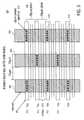
- FIG. 3is an illustration of an area of the die 302 having power 304 and 304 ′ and ground 303 ABM bars placed over ground 314 and 314 ′ and power 312 and 312 ′ lines existing within a metal layer of the die 302 and electrically interconnected with lined passivation openings (in the passivation and dielectric layers) 310 and 310 ′.
- the ABM bars 304 , 304 ′ and 303may be approximately 75 microns wide and spaced approximately 75 microns apart on the die 302 .
- the lined passivation openings 310 and 310 ′may be formed by an area that is approximately square with each side approximately 5 microns in length.
- a sufficient number of lined passivation openings 310 and 310 ′ between the ABM bars 304 , 304 ′ and 303 and the metal surfacecan be formed to interconnect the ABM bars 304 , 304 ′ and 303 to the respective power 312 and 312 ′ and ground 314 and 314 ′ lines.
- FIG. 3is an illustration of an area of the die 302 having power 304 and 304 ′ and ground 303 ABM bars placed over ground 312 and 312 ′ and power 314 and 314 ′ lines existing within a metal layer of the die 302 and electrically interconnected with lined passivation openings (in the passivation and dielectric layers) 310 and 310 ′.
- the ABM bars 304 , 304 ′ and 303may be approximately 75 microns wide and spaced approximately 75 microns apart on die 302 .
- the lined passivation openings 310 and 310 ′may be formed by an area that is approximately square with each side approximately 5 microns in length.
- a sufficient number of lined passivation openings 310 and 310 ′ between the ABM bars 304 , 304 ′ and 303 and the metal surfacecan be formed to interconnect the ABM bars 304 , 304 ′ and 303 to the respective power 314 and 314 ′ and ground 312 and 312 ′ lines.
- FIG. 3further illustrates the finer pitch 308 available (bars) 304 and 304 ′ than is available when using bumps (FIG. 1C above) to connect power and ground to circuitry outside the die 302 .
- the ABM bars 304 and 304 ′are better for power routing because they can more uniformly distribute power across the die 302 .
- the underlying power lines in the last metal layercan only occur under a bump, and bump pitch is limited to approximately 150 um due to process constraints.
- the power and ground linescan only be spaced every 75 microns.
- passivation openings 310can occur anywhere along the bar 304 and 304 ′, therefore power and ground lines (Vdd/Vss) 312 , 312 ′, 314 , and 314 ′ can be placed almost as often as desired, such as every 30 microns. Having more power and ground lines 312 , 312 ′, 314 , and 314 ′ that are spaced more closely together improves power delivery by reducing resistive drop and having lower inductance. The result is improved performance.
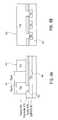
- FIGS. 4A & 4Billustrate side views of ABM ground bars 402 having interconnections (lined passivation openings) 404 to the M7 layer 406 .
- the interconnectspass through an Si 3 N 4 dielectric layer 408 and a polyimide passivation layer 410 .
- FIGS. 4A & 4Bshow the ABM ground bar 402 connecting to a copper ground line 410 fabricated from the M 7 406 layer while an adjacent ABM power bar 412 is separated from the ground line 410 by the Si 3 N 4 408 and polyimide 410 layers.
- FIGS. 5A-5Hillustrate a method for producing the ABM bars on the die.
- FIG. 5Aillustrates a final metal interconnect layer 501 such as M7 (deposited within a patterned dielectric layer) on a die 500 which can include a combination of power lines 502 and 502 ′ and ground lines 504 and 504 ′.
- a layer of a dielectric material 506such as silicon nitride (Si 3 N 4 ) or silicon carbide SiC is deposited over the surface of the die 500 that includes the etched M7 layer 501 .
- FIG. 5Cillustrates the deposit of a passivation layer 508 .
- the passivation layermay be a material such as a polyimide or silicon dioxide and is blanket deposited by sputtering, spinning, CVD, or rolling to cover the dielectric coating 506 .
- the surfacecan be patterned with a photoresist (not shown).
- FIG. 5Dillustrates passivation openings 510 and 510 ′ in the passivation layer 508 and the dielectric 506 layer, exposing areas of the metal power 502 and 502 ′, ground lines 504 and 504 ′ within M7 501 .
- the openings 510 and 510 ′may be created by first patterning with a photoresist (not shown) and then etching through the passivation 506 and dielectric 504 layers to expose lines 502 , 502 ′, 504 , and 504 ′ at M7 501 .
- FIG. 5Eis an illustration of lined passivation openings 512 and 512 ′ which are lined with a conductive metal or metal alloy. In an embodiment, the passivation openings 512 and 512 ′ have a dual layer (not shown) sputter lined with titanium and then copper.
- FIG. 5Fillustrates a patterned photoresist 514 applied over the passivation coating 506 .
- FIG. 5Gillustrates the results of an electroplating process to fill-in openings in the photoresist pattern 514 with copper 516 .
- FIG. 5Hillustrates a cross-section of the die 500 where the photoresist has been striped away with a solvent and number of ABM bars 518 and 518 ′ along with a copper signal bump 520 remain that are interconnected to lines 502 , 502 ′, 504 , and 504 ′ within M7 501 .
- FIGS. 6A & 6Billustrate a die-substrate assembly 600 .
- An assembly processsuch as an embodiment described in FIGS. 5A-5H above, can attach the die 602 to the substrate 604 .
- the substrate 604can be any mating component to connect the die 602 to outside circuitry, such as a package or printed circuit board where the substrate 604 can contain contacting ground 606 and 606 ′ and power 608 areas of solder 609 and 609 ′ to mate with the ground 610 and 610 ′ and power 612 bar areas on the die 602 .
- the solder 609 and 609 ′may be the low temperature solder such as lead tin or silver tin, that is coated over surfaces of copper beneath (not shown).
- a benefit of having equivalent mating solder areas 609 and 609 ′ on the substrate 604 to mate with the copper power 610 , and 610 ′ and ground 612 bars on the die 602 ,is that a rate of heat transfer from the die 602 , while the die is performing operations in a computer, can be increased.
- a heating cycleis then performed by placing the die-substrate assembly in a reflow oven that heats the solder until it flows as a liquid. After the reflow operation, the copper bumps are electrically and mechanically connected to the solder lands and the power/ground bars of the die are electrically and mechanically connected to the mating power/ground strips or lands on the substrate.
- a substratesuch as plastic packaging or a printed circuit board, that later mates with the die, may be passed through a soldering apparatus where one side is subjected to a soldering operation to solder hundreds of terminals on each of the substrates.
- wave soldering machinesfor this purpose is well known. These machines include conveyors that carry the boards over a molten bath of solder that is agitated to rise in waves against the undersides of the boards.
- a solder masking operationPrior to wave soldering, a solder masking operation is required to protect portions of the package substrate from being contacted by the hot molten solder.
- the solder maskis applied as one or more coatings through well-known techniques such as sputter, spray, or silk-screen such as through a steel screen mesh.
- solder maskWhen the solder mask is applied with a screen mesh, a pattern in the mesh can provide openings in the solder mask to be later filled with the solder operation.
- wave solderingis performed to fill-in the areas open in the mask. The cured solder mask remains on the finished substrate providing good dielectric coverage for the circuit lines to be protected.
Landscapes
- Engineering & Computer Science (AREA)
- Computer Hardware Design (AREA)
- Microelectronics & Electronic Packaging (AREA)
- Power Engineering (AREA)
- Physics & Mathematics (AREA)
- Condensed Matter Physics & Semiconductors (AREA)
- General Physics & Mathematics (AREA)
- Geometry (AREA)
- Internal Circuitry In Semiconductor Integrated Circuit Devices (AREA)
- Wire Bonding (AREA)
- Superconductor Devices And Manufacturing Methods Thereof (AREA)
- Coupling Device And Connection With Printed Circuit (AREA)
- Waveguides (AREA)
- Electric Connection Of Electric Components To Printed Circuits (AREA)
- Escalators And Moving Walkways (AREA)
- Replacing, Conveying, And Pick-Finding For Filamentary Materials (AREA)
- Forklifts And Lifting Vehicles (AREA)
- Production Of Multi-Layered Print Wiring Board (AREA)
Abstract
Description
1. Field of the Invention
This invention relates to the field of microchip packaging and in particular to routing power and ground connections between the microchip and the package substrate.
2. Discussion of Related Art
Integrated circuits that use high power levels, need a dense pattern of power and ground lines to deliver the required current and achieve expected performance. As the power requirements for a circuit increase, more of the normal interconnect layers (e.g. M5 and M6 on P860) are needed for routing power and ground and they are less available for routing signals. The need for routing power and ground must be addressed by adding more interconnect layers. FIG. 1A is an illustration of a die surface with a C4 bump pattern containing I/O for signal, power, and ground. Challenges to provide finer pitch bumps between a die and a die package have increased routing and routing complexity at the die surface. FIG. 1B is an illustration of a die surface with ABM bumps connected to ground (Vss) and power (Vdd) lines on the chip. With this design, minimum spacing between bumps is approximately 75 microns, bump diameters approximately 75 microns, with a minimum pitch of 150 microns to efficiently route signal lines.
An apparatus, comprising: a die having a surface, comprising: an array of electrically conductive bumps; and a plurality of electrically conductive bars positioned within the array of electrically conductive bumps.
FIG. 1A is an illustration of a die surface with a C4 bump pattern containing I/O for signal, power, and ground.
FIG. 1B is an illustration of a die surface with ABM bumps connected to ground (Vss) and power (Vdd) lines on the die.
FIG. 2A is an illustration of the die with power and ground bars using alternate bump metallurgy.
FIG. 2B is an illustration of the die with power and ground bars and an edge ring.
FIG. 3 is an illustration of ABM bars placed over ground and power lines existing within a metal layer and interconnected with lines passivation openings.
FIG. 4A is an illustration of the ABM bar connected to the M7 copper layer.
FIG. 4B is an illustration of the ABM bar connected to the M7 copper layer in a view rotated 90 degrees from that of FIG.4A.
FIGS. 5A-5H are illustrations of a method to produce ABM bars on the die.
FIG. 5A is an illustration of the die containing power and ground lines within a metal layer.
FIG. 5B is an illustration of the die have a dielectric layer deposited over the metal layer.
FIG. 5C is an illustration of the die having a passivation layer deposited over the dielectric layer.
FIG. 5D is an illustration of the die having passivation openings etched through the dielectric layer and the passivation layer.
FIG. 5E is an illustration of the die having lined passivation openings.
FIG. 5F is an illustration of the die having a patterned photoresist layer.
FIG. 5G is an illustration of the die having the patterns filled in with copper.
FIG. 5H is an illustration of the die with power bars, ground bars, and a bump having alternate bump metallurgy.
FIGS. 6A and 6B illustrate a die-substrate assembly 600.
A structure and method for providing power and ground bars, centered within an array of I/O signal bumps on a die surface is disclosed. In an embodiment, the I/O signal bumps and the power and ground bars could be in the form of copper bumps. The structure and method can provide an efficient means of connecting power and ground between a microchip (die) and a substrate. The structure and method can make use of a bump metallurgy that is different from solder (i.e. alternate bump metallurgy or ABM). As a result, the power and ground structures can be located on the die with the I/O signal bumps (signal bumps), positioned in an ordered array, surrounding the power and ground structures.
A structure and method for providing power and ground bars, centered within an array of I/O signal bumps on a die surface is disclosed. In an embodiment, the I/O signal bumps and the power and ground bars could be in the form of copper bumps. The structure and method can provide an efficient means of connecting power and ground between a microchip (die) and a substrate. The structure and method can make use of a bump metallurgy that is different from solder (i.e. alternate bump metallurgy or ABM). As a result, the power and ground structures can be located on the die with the I/O signal bumps (signal bumps), positioned in an ordered array, surrounding. As a further result, the power and ground structures can be fabricated from the same metal layer as the signal bumps. This structure and method allows for the placement of more power and ground lines within the interconnect metal layers since tighter spacing can be used.
In an embodiment, at assembly, the signal bumps on the die can mate with respective solder lands on a substrate such as a die package. The die package can have a number of solder lands to be in contact with the power and ground bars on the die as well as the signal bumps. Alternatively, the solder lands can cover a large enough area to contact the entire surface of one or more of the power bars and/or ground bars. The power bars and ground bars, and the mating solder lands, may take on any shape from square to a number of linear strips.
In the following description numerous specific details are set forth such as specific materials, equipment, and processes in order to provide a thorough understanding of the present invention. In other instances, well known computer assembly techniques and machinery have not been set forth in detail in order to minimize obscuring the present invention.
FIGS. 2A & 2B are illustrations of the die202 with power and ground bars204 using alternate bump metallurgy (ABM). In an embodiment as shown in FIG. 2A, the signal bumps206 are placed in an arrayed pattern having the power and ground bars204 positioned within. In an alternate embodiment, FIG. 2B, an additional series of bars are placed at the periphery of the signal bumps, i.e. the edge of the wafer. The purpose of the edge bars is to provide an improved seal when the die is attached to a substrate such as plastic packaging. In an embodiment, the power and ground bars204 can be formed in the shape of rectangles and separated from the top metal by a dielectric and a passivation coating. The power and ground bars can be subsequently coated with a thin layer of a low temperature solder to improve their electrical contact with the mating solder lands or bars on the mating substrate.
FIG. 3 is an illustration of an area of thedie 302 havingpower ground 303 ABM bars placed overground power die 302 and electrically interconnected with lined passivation openings (in the passivation and dielectric layers)310 and310′. The ABM bars304,304′ and303 may be approximately 75 microns wide and spaced approximately 75 microns apart on thedie 302. The linedpassivation openings passivation openings respective power ground
FIG. 3 is an illustration of an area of thedie 302 havingpower ground 303 ABM bars placed overground power die 302 and electrically interconnected with lined passivation openings (in the passivation and dielectric layers)310 and310′. The ABM bars304,304′ and303 may be approximately 75 microns wide and spaced approximately 75 microns apart ondie 302. The linedpassivation openings passivation openings respective power ground
FIG. 3 further illustrates thefiner pitch 308 available (bars)304 and304′ than is available when using bumps (FIG. 1C above) to connect power and ground to circuitry outside thedie 302. The ABM bars304 and304′ are better for power routing because they can more uniformly distribute power across thedie 302. For ABM bumps (FIG. 1B above), the underlying power lines in the last metal layer can only occur under a bump, and bump pitch is limited to approximately 150 um due to process constraints. The power and ground lines can only be spaced every 75 microns. Returning to FIG. 3, withABM bars passivation openings 310 can occur anywhere along thebar ground lines
FIGS. 4A & 4B illustrate side views of ABM ground bars402 having interconnections (lined passivation openings)404 to theM7 layer 406. In an embodiment, the interconnects pass through an Si3N4dielectric layer 408 and apolyimide passivation layer 410. FIGS. 4A & 4B show theABM ground bar 402 connecting to acopper ground line 410 fabricated from theM7 406 layer while an adjacentABM power bar 412 is separated from theground line 410 by the Si3N4408 andpolyimide 410 layers.
FIGS. 5A-5H illustrate a method for producing the ABM bars on the die. FIG. 5A illustrates a finalmetal interconnect layer 501 such as M7 (deposited within a patterned dielectric layer) on adie 500 which can include a combination ofpower lines ground lines dielectric material 506 such as silicon nitride (Si3N4) or silicon carbide SiC is deposited over the surface of the die500 that includes the etchedM7 layer 501. FIG. 5C illustrates the deposit of apassivation layer 508. In an embodiment, the passivation layer may be a material such as a polyimide or silicon dioxide and is blanket deposited by sputtering, spinning, CVD, or rolling to cover thedielectric coating 506. After application of the passivation layer, the surface can be patterned with a photoresist (not shown). FIG. 5D illustratespassivation openings passivation layer 508 and the dielectric506 layer, exposing areas of themetal power ground lines M7 501. Theopenings passivation 506 and dielectric504 layers to exposelines M7 501. FIG. 5E is an illustration of linedpassivation openings passivation openings photoresist 514 applied over thepassivation coating 506. FIG. 5G illustrates the results of an electroplating process to fill-in openings in thephotoresist pattern 514 withcopper 516. FIG. 5H illustrates a cross-section of thedie 500 where the photoresist has been striped away with a solvent and number of ABM bars518 and518′ along with acopper signal bump 520 remain that are interconnected tolines M7 501.
FIGS. 6A & 6B illustrate a die-substrate assembly 600. An assembly process, such as an embodiment described in FIGS. 5A-5H above, can attach thedie 602 to thesubstrate 604. Thesubstrate 604 can be any mating component to connect thedie 602 to outside circuitry, such as a package or printed circuit board where thesubstrate 604 can contain contactingground power 608 areas ofsolder ground power 612 bar areas on thedie 602. Thesolder mating solder areas substrate 604 to mate with thecopper power die 602, is that a rate of heat transfer from thedie 602, while the die is performing operations in a computer, can be increased.
A heating cycle is then performed by placing the die-substrate assembly in a reflow oven that heats the solder until it flows as a liquid. After the reflow operation, the copper bumps are electrically and mechanically connected to the solder lands and the power/ground bars of the die are electrically and mechanically connected to the mating power/ground strips or lands on the substrate.
During production, a substrate such as plastic packaging or a printed circuit board, that later mates with the die, may be passed through a soldering apparatus where one side is subjected to a soldering operation to solder hundreds of terminals on each of the substrates. The use of wave soldering machines for this purpose is well known. These machines include conveyors that carry the boards over a molten bath of solder that is agitated to rise in waves against the undersides of the boards. Prior to wave soldering, a solder masking operation is required to protect portions of the package substrate from being contacted by the hot molten solder. The solder mask is applied as one or more coatings through well-known techniques such as sputter, spray, or silk-screen such as through a steel screen mesh. When the solder mask is applied with a screen mesh, a pattern in the mesh can provide openings in the solder mask to be later filled with the solder operation. After cure of the solder masking, wave soldering is performed to fill-in the areas open in the mask. The cured solder mask remains on the finished substrate providing good dielectric coverage for the circuit lines to be protected.
Claims (5)
1. A method, comprising:
depositing a dielectric layer over a top metal layer of a die having one or more power lines and one or more ground lines formed thereon;
depositing a passivation layer upon the dielectric layer;
creating one or more passivation openings in the dielectric layer and the passivation layer such that a portion of at least one of the power lines and ground lines is exposed;
lining the passivation openings with a conductive material; and
depositing a plurality of electrically conductive bars on the top surface of the passivation layer that are in contact with the lined passivation openings.
2. The method ofclaim 1 further comprising:
placing an array of solder lands on a substrate; and
connecting the die to the substrate such that the array of solder lands mate with the plurality of electrically conductive bars on the die.
3. The method ofclaim 2 wherein at least one of the electrically conductive bars connects to power.
4. The method ofclaim 2 wherein at least one of the electrically conductive bars connects to ground.
5. The method ofclaim 2 wherein the plurality of the electrically conductive bars forms a periphery around the die.
Priority Applications (8)
| Application Number | Priority Date | Filing Date | Title |
|---|---|---|---|
| US09/823,427US6653563B2 (en) | 2001-03-30 | 2001-03-30 | Alternate bump metallurgy bars for power and ground routing |
| AT02721543TATE347176T1 (en) | 2001-03-30 | 2002-03-22 | SOLDER BUMP METALLURGICAL RAILS FOR SUPPLY AND GROUND LINE ROUTING |
| AU2002252469AAU2002252469A1 (en) | 2001-03-30 | 2002-03-22 | Alternate bump metallurgy bars for power and ground routing |
| CNB028076249ACN100440504C (en) | 2001-03-30 | 2002-03-22 | Method of forming bars of power and ground wiring by staggered bump metallurgy |
| EP02721543AEP1374306B1 (en) | 2001-03-30 | 2002-03-22 | Bump metallurgy bars for power and ground routing |
| PCT/US2002/008905WO2002080273A2 (en) | 2001-03-30 | 2002-03-22 | Alternate bump metallurgy bars for power and ground routing |
| DE60216433TDE60216433T2 (en) | 2001-03-30 | 2002-03-22 | LOTHÖCKMETALLURGI RAILS FOR SUPPLY AND MASS GUIDANCE |
| TW091106311ATW557553B (en) | 2001-03-30 | 2002-03-29 | Alternate bump metallurgy bars for power and ground routing |
Applications Claiming Priority (1)
| Application Number | Priority Date | Filing Date | Title |
|---|---|---|---|
| US09/823,427US6653563B2 (en) | 2001-03-30 | 2001-03-30 | Alternate bump metallurgy bars for power and ground routing |
Publications (2)
| Publication Number | Publication Date |
|---|---|
| US20020141171A1 US20020141171A1 (en) | 2002-10-03 |
| US6653563B2true US6653563B2 (en) | 2003-11-25 |
Family
ID=25238741
Family Applications (1)
| Application Number | Title | Priority Date | Filing Date |
|---|---|---|---|
| US09/823,427Expired - LifetimeUS6653563B2 (en) | 2001-03-30 | 2001-03-30 | Alternate bump metallurgy bars for power and ground routing |
Country Status (8)
| Country | Link |
|---|---|
| US (1) | US6653563B2 (en) |
| EP (1) | EP1374306B1 (en) |
| CN (1) | CN100440504C (en) |
| AT (1) | ATE347176T1 (en) |
| AU (1) | AU2002252469A1 (en) |
| DE (1) | DE60216433T2 (en) |
| TW (1) | TW557553B (en) |
| WO (1) | WO2002080273A2 (en) |
Cited By (42)
| Publication number | Priority date | Publication date | Assignee | Title |
|---|---|---|---|---|
| US20070205520A1 (en)* | 2006-03-02 | 2007-09-06 | Megica Corporation | Chip package and method for fabricating the same |
| US20080003806A1 (en)* | 2000-10-18 | 2008-01-03 | Megica Corporation | Post passivation interconnection schemes on top of IC chip |
| US20080006945A1 (en)* | 2006-06-27 | 2008-01-10 | Megica Corporation | Integrated circuit and method for fabricating the same |
| US20080048320A1 (en)* | 2001-03-05 | 2008-02-28 | Megica Corporation | Low fabrication cost, fine pitch and high reliability solder bump |
| US20080113504A1 (en)* | 2002-05-01 | 2008-05-15 | Megica Corporation | Low fabrication cost, high performance, high reliability chip scale package |
| US20080116581A1 (en)* | 2003-10-15 | 2008-05-22 | Megica Corporation | Post passivation interconnection schemes on top of the ic chips |
| US20080211105A1 (en)* | 2002-10-25 | 2008-09-04 | Megica Corporation | Method of assembling chips |
| US20090057901A1 (en)* | 2001-09-17 | 2009-03-05 | Megica Corporation | Structure of high performance combo chip and processing method |
| US20090057894A1 (en)* | 2004-07-09 | 2009-03-05 | Megica Corporation | Structure of Gold Bumps and Gold Conductors on one IC Die and Methods of Manufacturing the Structures |
| US20090065871A1 (en)* | 2005-09-23 | 2009-03-12 | Megica Corporation | Semiconductor chip and process for forming the same |
| US20090146305A1 (en)* | 2004-10-12 | 2009-06-11 | Megica Corporation | Post passivation interconnection schemes on top of the ic chips |
| US20090267213A1 (en)* | 2001-03-05 | 2009-10-29 | Megica Corporation | Structure and manufacturing method of a chip scale package with low fabrication cost, fine pitch and high reliability solder bump |
| US7645293B2 (en) | 2004-04-21 | 2010-01-12 | United States Surgical Corporation | Suture anchor installation system and method |
| US7855461B2 (en) | 2003-12-08 | 2010-12-21 | Megica Corporation | Chip structure with bumps and testing pads |
| US7863654B2 (en) | 1998-12-21 | 2011-01-04 | Megica Corporation | Top layers of metal for high performance IC's |
| US7898058B2 (en) | 2001-12-31 | 2011-03-01 | Megica Corporation | Integrated chip package structure using organic substrate and method of manufacturing the same |
| US7906422B2 (en) | 1998-12-21 | 2011-03-15 | Megica Corporation | Chip structure and process for forming the same |
| US7915734B2 (en) | 2001-12-13 | 2011-03-29 | Megica Corporation | Chip structure and process for forming the same |
| US7960270B2 (en) | 2002-01-07 | 2011-06-14 | Megica Corporation | Method for fabricating circuit component |
| US7960269B2 (en) | 2005-07-22 | 2011-06-14 | Megica Corporation | Method for forming a double embossing structure |
| US7964973B2 (en) | 2004-08-12 | 2011-06-21 | Megica Corporation | Chip structure |
| US7969006B2 (en) | 2006-09-29 | 2011-06-28 | Megica Corporation | Integrated circuit chips with fine-line metal and over-passivation metal |
| US8004092B2 (en) | 2005-10-28 | 2011-08-23 | Megica Corporation | Semiconductor chip with post-passivation scheme formed over passivation layer |
| US8013449B2 (en) | 2003-10-15 | 2011-09-06 | Megica Corporation | Post passivation interconnection schemes on top of the IC chips |
| US8022546B2 (en) | 1998-12-21 | 2011-09-20 | Megica Corporation | Top layers of metal for high performance IC's |
| US8021976B2 (en) | 2002-10-15 | 2011-09-20 | Megica Corporation | Method of wire bonding over active area of a semiconductor circuit |
| US8022544B2 (en) | 2004-07-09 | 2011-09-20 | Megica Corporation | Chip structure |
| US8030775B2 (en) | 2007-08-27 | 2011-10-04 | Megica Corporation | Wirebond over post passivation thick metal |
| US20110283034A1 (en)* | 2010-05-12 | 2011-11-17 | Samsung Electronics Co., Ltd. | Semiconductor chip, and semiconductor package and system each including the semiconductor chip |
| US8067837B2 (en) | 2004-09-20 | 2011-11-29 | Megica Corporation | Metallization structure over passivation layer for IC chip |
| US8148806B2 (en) | 2000-05-19 | 2012-04-03 | Megica Corporation | Multiple chips bonded to packaging structure with low noise and multiple selectable functions |
| US8178967B2 (en) | 2001-09-17 | 2012-05-15 | Megica Corporation | Low fabrication cost, high performance, high reliability chip scale package |
| US8193636B2 (en) | 2007-03-13 | 2012-06-05 | Megica Corporation | Chip assembly with interconnection by metal bump |
| US20120145439A1 (en)* | 2010-12-10 | 2012-06-14 | Askey Computer Corp. | Printed circuit board grounding structure for use with communication apparatus |
| US8242601B2 (en) | 2004-10-29 | 2012-08-14 | Megica Corporation | Semiconductor chip with passivation layer comprising metal interconnect and contact pads |
| US8294279B2 (en) | 2005-01-25 | 2012-10-23 | Megica Corporation | Chip package with dam bar restricting flow of underfill |
| US8304907B2 (en) | 1998-12-21 | 2012-11-06 | Megica Corporation | Top layers of metal for integrated circuits |
| US8492870B2 (en) | 2002-01-19 | 2013-07-23 | Megica Corporation | Semiconductor package with interconnect layers |
| US8535976B2 (en) | 2001-12-31 | 2013-09-17 | Megica Corporation | Method for fabricating chip package with die and substrate |
| US8901733B2 (en) | 2001-02-15 | 2014-12-02 | Qualcomm Incorporated | Reliable metal bumps on top of I/O pads after removal of test probe marks |
| US9030029B2 (en) | 2001-12-31 | 2015-05-12 | Qualcomm Incorporated | Chip package with die and substrate |
| US11508696B2 (en)* | 2017-06-20 | 2022-11-22 | Taiwan Semiconductor Manufacturing Company Ltd. | Semiconductor device |
Families Citing this family (6)
| Publication number | Priority date | Publication date | Assignee | Title |
|---|---|---|---|---|
| JP3768433B2 (en)* | 2001-11-19 | 2006-04-19 | 株式会社ルネサステクノロジ | Semiconductor device design method |
| US20050133933A1 (en)* | 2003-12-19 | 2005-06-23 | Advanpack Solutions Pte. Ltd. | Various structure/height bumps for wafer level-chip scale package |
| TWI286916B (en)* | 2004-10-18 | 2007-09-11 | Via Tech Inc | Circuit structure |
| US20090148594A1 (en)* | 2007-08-15 | 2009-06-11 | Tessera, Inc. | Interconnection element with plated posts formed on mandrel |
| JP5538682B2 (en)* | 2008-03-06 | 2014-07-02 | ピーエスフォー ルクスコ エスエイアールエル | Semiconductor device and manufacturing method thereof |
| JP6334851B2 (en)* | 2013-06-07 | 2018-05-30 | シナプティクス・ジャパン合同会社 | Semiconductor device, display device module, and display device module manufacturing method |
Citations (12)
| Publication number | Priority date | Publication date | Assignee | Title |
|---|---|---|---|---|
| US4710798A (en) | 1985-09-10 | 1987-12-01 | Northern Telecom Limited | Integrated circuit chip package |
| JPS6415737A (en) | 1987-06-16 | 1989-01-19 | Agfa Gevaert Nv | Polymer phosphonium mordant and photographic material |
| EP0361825A2 (en) | 1988-09-28 | 1990-04-04 | Nec Corporation | Semiconductor chip and method of manufacturing it |
| US5083187A (en) | 1990-05-16 | 1992-01-21 | Texas Instruments Incorporated | Integrated circuit device having bumped power supply buses over active surface areas and method of manufacture thereof |
| US5336992A (en)* | 1992-06-03 | 1994-08-09 | Trw Inc. | On-wafer integrated circuit electrical testing |
| JPH10301301A (en) | 1997-04-28 | 1998-11-13 | Hitachi Electron Eng Co Ltd | Gap window position detection method |
| US5886409A (en)* | 1996-01-16 | 1999-03-23 | Hitachi, Ltd. | Electrode structure of wiring substrate of semiconductor device having expanded pitch |
| JPH11111074A (en) | 1997-10-03 | 1999-04-23 | Yazaki Corp | Fire resistant wire |
| US5943597A (en)* | 1998-06-15 | 1999-08-24 | Motorola, Inc. | Bumped semiconductor device having a trench for stress relief |
| US6057596A (en) | 1998-10-19 | 2000-05-02 | Silicon Integrated Systems Corp. | Chip carrier having a specific power join distribution structure |
| US6171888B1 (en)* | 1996-03-08 | 2001-01-09 | Lsi Logic Corp. | Multi-layer tab tape having distinct signal, power and ground planes, semiconductor device assembly employing same, apparatus for and method of assembling same |
| US6307256B1 (en)* | 1998-10-26 | 2001-10-23 | Apack Technologies Inc. | Semiconductor package with a stacked chip on a leadframe |
Family Cites Families (8)
| Publication number | Priority date | Publication date | Assignee | Title |
|---|---|---|---|---|
| JP2624320B2 (en)* | 1989-01-24 | 1997-06-25 | 三菱電機株式会社 | Semiconductor device |
| JPH0555228A (en)* | 1991-08-27 | 1993-03-05 | Nec Corp | Semiconductor device |
| US5406122A (en)* | 1993-10-27 | 1995-04-11 | Hughes Aircraft Company | Microelectronic circuit structure including conductor bridges encapsulated in inorganic dielectric passivation layer |
| US5656858A (en)* | 1994-10-19 | 1997-08-12 | Nippondenso Co., Ltd. | Semiconductor device with bump structure |
| US5872051A (en)* | 1995-08-02 | 1999-02-16 | International Business Machines Corporation | Process for transferring material to semiconductor chip conductive pads using a transfer substrate |
| JP2000133668A (en)* | 1998-10-22 | 2000-05-12 | Sony Corp | Semiconductor device and packaging structure |
| JP3813367B2 (en)* | 1998-12-22 | 2006-08-23 | 三洋電機株式会社 | Semiconductor device and manufacturing method thereof |
| JP3647307B2 (en)* | 1999-04-19 | 2005-05-11 | キヤノン株式会社 | Printed circuit board and electronic device |
- 2001
- 2001-03-30USUS09/823,427patent/US6653563B2/ennot_activeExpired - Lifetime
- 2002
- 2002-03-22WOPCT/US2002/008905patent/WO2002080273A2/enactiveIP Right Grant
- 2002-03-22DEDE60216433Tpatent/DE60216433T2/ennot_activeExpired - Lifetime
- 2002-03-22CNCNB028076249Apatent/CN100440504C/ennot_activeExpired - Lifetime
- 2002-03-22EPEP02721543Apatent/EP1374306B1/ennot_activeExpired - Lifetime
- 2002-03-22ATAT02721543Tpatent/ATE347176T1/ennot_activeIP Right Cessation
- 2002-03-22AUAU2002252469Apatent/AU2002252469A1/ennot_activeAbandoned
- 2002-03-29TWTW091106311Apatent/TW557553B/ennot_activeIP Right Cessation
Patent Citations (12)
| Publication number | Priority date | Publication date | Assignee | Title |
|---|---|---|---|---|
| US4710798A (en) | 1985-09-10 | 1987-12-01 | Northern Telecom Limited | Integrated circuit chip package |
| JPS6415737A (en) | 1987-06-16 | 1989-01-19 | Agfa Gevaert Nv | Polymer phosphonium mordant and photographic material |
| EP0361825A2 (en) | 1988-09-28 | 1990-04-04 | Nec Corporation | Semiconductor chip and method of manufacturing it |
| US5083187A (en) | 1990-05-16 | 1992-01-21 | Texas Instruments Incorporated | Integrated circuit device having bumped power supply buses over active surface areas and method of manufacture thereof |
| US5336992A (en)* | 1992-06-03 | 1994-08-09 | Trw Inc. | On-wafer integrated circuit electrical testing |
| US5886409A (en)* | 1996-01-16 | 1999-03-23 | Hitachi, Ltd. | Electrode structure of wiring substrate of semiconductor device having expanded pitch |
| US6171888B1 (en)* | 1996-03-08 | 2001-01-09 | Lsi Logic Corp. | Multi-layer tab tape having distinct signal, power and ground planes, semiconductor device assembly employing same, apparatus for and method of assembling same |
| JPH10301301A (en) | 1997-04-28 | 1998-11-13 | Hitachi Electron Eng Co Ltd | Gap window position detection method |
| JPH11111074A (en) | 1997-10-03 | 1999-04-23 | Yazaki Corp | Fire resistant wire |
| US5943597A (en)* | 1998-06-15 | 1999-08-24 | Motorola, Inc. | Bumped semiconductor device having a trench for stress relief |
| US6057596A (en) | 1998-10-19 | 2000-05-02 | Silicon Integrated Systems Corp. | Chip carrier having a specific power join distribution structure |
| US6307256B1 (en)* | 1998-10-26 | 2001-10-23 | Apack Technologies Inc. | Semiconductor package with a stacked chip on a leadframe |
Non-Patent Citations (1)
| Title |
|---|
| PCT Search Report, International Application No.: PCT/US 02/08905, Apr. 10, 2003. |
Cited By (124)
| Publication number | Priority date | Publication date | Assignee | Title |
|---|---|---|---|---|
| US8350386B2 (en) | 1998-12-21 | 2013-01-08 | Megica Corporation | Top layers of metal for high performance IC's |
| US8304907B2 (en) | 1998-12-21 | 2012-11-06 | Megica Corporation | Top layers of metal for integrated circuits |
| US8022545B2 (en) | 1998-12-21 | 2011-09-20 | Megica Corporation | Top layers of metal for high performance IC's |
| US8138079B2 (en) | 1998-12-21 | 2012-03-20 | Megica Corporation | Method of wire bonding over active area of a semiconductor circuit |
| US8022546B2 (en) | 1998-12-21 | 2011-09-20 | Megica Corporation | Top layers of metal for high performance IC's |
| US7999384B2 (en) | 1998-12-21 | 2011-08-16 | Megica Corporation | Top layers of metal for high performance IC's |
| US8035227B2 (en) | 1998-12-21 | 2011-10-11 | Megica Corporation | Top layers of metal for high performance IC's |
| US8415800B2 (en) | 1998-12-21 | 2013-04-09 | Megica Corporation | Top layers of metal for high performance IC's |
| US7915157B2 (en) | 1998-12-21 | 2011-03-29 | Megica Corporation | Chip structure and process for forming the same |
| US7906422B2 (en) | 1998-12-21 | 2011-03-15 | Megica Corporation | Chip structure and process for forming the same |
| US7906849B2 (en) | 1998-12-21 | 2011-03-15 | Megica Corporation | Chip structure and process for forming the same |
| US7884479B2 (en) | 1998-12-21 | 2011-02-08 | Megica Corporation | Top layers of metal for high performance IC's |
| US8471384B2 (en) | 1998-12-21 | 2013-06-25 | Megica Corporation | Top layers of metal for high performance IC's |
| US7863654B2 (en) | 1998-12-21 | 2011-01-04 | Megica Corporation | Top layers of metal for high performance IC's |
| US8531038B2 (en) | 1998-12-21 | 2013-09-10 | Megica Corporation | Top layers of metal for high performance IC's |
| US8148806B2 (en) | 2000-05-19 | 2012-04-03 | Megica Corporation | Multiple chips bonded to packaging structure with low noise and multiple selectable functions |
| US20080042293A1 (en)* | 2000-10-18 | 2008-02-21 | Megica Corporation | Post passivation interconnection schemes on top of IC chip |
| US20080067694A1 (en)* | 2000-10-18 | 2008-03-20 | Megica Corporation | Post passivation interconnection schemes on top of IC chip |
| US20080001300A1 (en)* | 2000-10-18 | 2008-01-03 | Megica Corporation | Post passivation interconnection schemes on top of IC chip |
| US8188603B2 (en) | 2000-10-18 | 2012-05-29 | Megica Corporation | Post passivation interconnection schemes on top of IC chip |
| US8004088B2 (en) | 2000-10-18 | 2011-08-23 | Megica Corporation | Post passivation interconnection schemes on top of IC chip |
| US20080045008A1 (en)* | 2000-10-18 | 2008-02-21 | Megica Corporation | Post passivation interconnection schemes on top of IC chip |
| US8492900B2 (en) | 2000-10-18 | 2013-07-23 | Megica Corporation | Post passivation interconnection schemes on top of IC chip |
| US8482127B2 (en) | 2000-10-18 | 2013-07-09 | Megica Corporation | Post passivation interconnection schemes on top of IC chip |
| USRE43674E1 (en) | 2000-10-18 | 2012-09-18 | Megica Corporation | Post passivation metal scheme for high-performance integrated circuit devices |
| US20080045002A1 (en)* | 2000-10-18 | 2008-02-21 | Megica Corporation | Post passivation interconnection schemes on top of IC chip |
| US7915161B2 (en) | 2000-10-18 | 2011-03-29 | Megica Corporation | Post passivation interconnection schemes on top of IC chip |
| US7919865B2 (en) | 2000-10-18 | 2011-04-05 | Megica Corporation | Post passivation interconnection schemes on top of IC chip |
| US7892965B2 (en) | 2000-10-18 | 2011-02-22 | Megica Corporation | Post passivation interconnection schemes on top of IC chip |
| US7923366B2 (en) | 2000-10-18 | 2011-04-12 | Megica Corporation | Post passivation interconnection schemes on top of IC chip |
| US7902067B2 (en) | 2000-10-18 | 2011-03-08 | Megica Corporation | Post passivation interconnection schemes on top of the IC chips |
| US20080042285A1 (en)* | 2000-10-18 | 2008-02-21 | Megica Corporation | Post passivation interconnection schemes on top of IC chip |
| US20080003806A1 (en)* | 2000-10-18 | 2008-01-03 | Megica Corporation | Post passivation interconnection schemes on top of IC chip |
| US20080061444A1 (en)* | 2000-10-18 | 2008-03-13 | Megica Corporation | Post passivation interconnection schemes on top of IC chip |
| US8435883B2 (en) | 2000-10-18 | 2013-05-07 | Megica Corporation | Post passivation interconnection schemes on top of IC chips |
| US8461686B2 (en) | 2000-10-18 | 2013-06-11 | Megica Corporation | Post passivation interconnection schemes on top of IC chip |
| US8901733B2 (en) | 2001-02-15 | 2014-12-02 | Qualcomm Incorporated | Reliable metal bumps on top of I/O pads after removal of test probe marks |
| US8158508B2 (en) | 2001-03-05 | 2012-04-17 | Megica Corporation | Structure and manufacturing method of a chip scale package |
| US20080054459A1 (en)* | 2001-03-05 | 2008-03-06 | Megica Corporation | Low fabrication cost, fine pitch and high reliability solder bump |
| US8072070B2 (en) | 2001-03-05 | 2011-12-06 | Megica Corporation | Low fabrication cost, fine pitch and high reliability solder bump |
| US7863739B2 (en) | 2001-03-05 | 2011-01-04 | Megica Corporation | Low fabrication cost, fine pitch and high reliability solder bump |
| US20080048320A1 (en)* | 2001-03-05 | 2008-02-28 | Megica Corporation | Low fabrication cost, fine pitch and high reliability solder bump |
| US20090261473A1 (en)* | 2001-03-05 | 2009-10-22 | Megica Corporation | Low fabrication cost, fine pitch and high reliability solder bump |
| US8368213B2 (en) | 2001-03-05 | 2013-02-05 | Megica Corporation | Low fabrication cost, fine pitch and high reliability solder bump |
| US20090267213A1 (en)* | 2001-03-05 | 2009-10-29 | Megica Corporation | Structure and manufacturing method of a chip scale package with low fabrication cost, fine pitch and high reliability solder bump |
| US7902679B2 (en) | 2001-03-05 | 2011-03-08 | Megica Corporation | Structure and manufacturing method of a chip scale package with low fabrication cost, fine pitch and high reliability solder bump |
| US7960212B2 (en) | 2001-09-17 | 2011-06-14 | Megica Corporation | Structure of high performance combo chip and processing method |
| US7960842B2 (en) | 2001-09-17 | 2011-06-14 | Megica Corporation | Structure of high performance combo chip and processing method |
| US7919873B2 (en) | 2001-09-17 | 2011-04-05 | Megica Corporation | Structure of high performance combo chip and processing method |
| US20090057901A1 (en)* | 2001-09-17 | 2009-03-05 | Megica Corporation | Structure of high performance combo chip and processing method |
| US8178967B2 (en) | 2001-09-17 | 2012-05-15 | Megica Corporation | Low fabrication cost, high performance, high reliability chip scale package |
| US9369175B2 (en) | 2001-09-17 | 2016-06-14 | Qualcomm Incorporated | Low fabrication cost, high performance, high reliability chip scale package |
| US8124446B2 (en) | 2001-09-17 | 2012-02-28 | Megica Corporation | Structure of high performance combo chip and processing method |
| US8008776B2 (en) | 2001-12-13 | 2011-08-30 | Megica Corporation | Chip structure and process for forming the same |
| US7932603B2 (en) | 2001-12-13 | 2011-04-26 | Megica Corporation | Chip structure and process for forming the same |
| US7919867B2 (en) | 2001-12-13 | 2011-04-05 | Megica Corporation | Chip structure and process for forming the same |
| US8546947B2 (en)* | 2001-12-13 | 2013-10-01 | Megica Corporation | Chip structure and process for forming the same |
| US7915734B2 (en) | 2001-12-13 | 2011-03-29 | Megica Corporation | Chip structure and process for forming the same |
| US20110278727A1 (en)* | 2001-12-13 | 2011-11-17 | Megica Corporation | Chip structure and process for forming the same |
| US9030029B2 (en) | 2001-12-31 | 2015-05-12 | Qualcomm Incorporated | Chip package with die and substrate |
| US9136246B2 (en) | 2001-12-31 | 2015-09-15 | Qualcomm Incorporated | Integrated chip package structure using silicon substrate and method of manufacturing the same |
| US7898058B2 (en) | 2001-12-31 | 2011-03-01 | Megica Corporation | Integrated chip package structure using organic substrate and method of manufacturing the same |
| US8471361B2 (en) | 2001-12-31 | 2013-06-25 | Megica Corporation | Integrated chip package structure using organic substrate and method of manufacturing the same |
| US8835221B2 (en) | 2001-12-31 | 2014-09-16 | Qualcomm Incorporated | Integrated chip package structure using ceramic substrate and method of manufacturing the same |
| US8535976B2 (en) | 2001-12-31 | 2013-09-17 | Megica Corporation | Method for fabricating chip package with die and substrate |
| US8461679B2 (en) | 2002-01-07 | 2013-06-11 | Megica Corporation | Method for fabricating circuit component |
| US7960270B2 (en) | 2002-01-07 | 2011-06-14 | Megica Corporation | Method for fabricating circuit component |
| US8890336B2 (en) | 2002-01-07 | 2014-11-18 | Qualcomm Incorporated | Cylindrical bonding structure and method of manufacture |
| US8492870B2 (en) | 2002-01-19 | 2013-07-23 | Megica Corporation | Semiconductor package with interconnect layers |
| US8481418B2 (en) | 2002-05-01 | 2013-07-09 | Megica Corporation | Low fabrication cost, high performance, high reliability chip scale package |
| US20080113504A1 (en)* | 2002-05-01 | 2008-05-15 | Megica Corporation | Low fabrication cost, high performance, high reliability chip scale package |
| US8026588B2 (en) | 2002-10-15 | 2011-09-27 | Megica Corporation | Method of wire bonding over active area of a semiconductor circuit |
| US8742580B2 (en) | 2002-10-15 | 2014-06-03 | Megit Acquisition Corp. | Method of wire bonding over active area of a semiconductor circuit |
| US9153555B2 (en) | 2002-10-15 | 2015-10-06 | Qualcomm Incorporated | Method of wire bonding over active area of a semiconductor circuit |
| US8021976B2 (en) | 2002-10-15 | 2011-09-20 | Megica Corporation | Method of wire bonding over active area of a semiconductor circuit |
| US9142527B2 (en) | 2002-10-15 | 2015-09-22 | Qualcomm Incorporated | Method of wire bonding over active area of a semiconductor circuit |
| US20080211105A1 (en)* | 2002-10-25 | 2008-09-04 | Megica Corporation | Method of assembling chips |
| US8421222B2 (en) | 2002-10-25 | 2013-04-16 | Megica Corporation | Chip package having a chip combined with a substrate via a copper pillar |
| US8021921B2 (en) | 2002-10-25 | 2011-09-20 | Megica Corporation | Method of joining chips utilizing copper pillar |
| US8456013B2 (en) | 2003-10-15 | 2013-06-04 | Megica Corporation | Post passivation interconnection schemes on top of the IC chips |
| US8013449B2 (en) | 2003-10-15 | 2011-09-06 | Megica Corporation | Post passivation interconnection schemes on top of the IC chips |
| US7928576B2 (en) | 2003-10-15 | 2011-04-19 | Megica Corporation | Post passivation interconnection schemes on top of the IC chips |
| US20080116581A1 (en)* | 2003-10-15 | 2008-05-22 | Megica Corporation | Post passivation interconnection schemes on top of the ic chips |
| US7855461B2 (en) | 2003-12-08 | 2010-12-21 | Megica Corporation | Chip structure with bumps and testing pads |
| US7645293B2 (en) | 2004-04-21 | 2010-01-12 | United States Surgical Corporation | Suture anchor installation system and method |
| US20100179592A1 (en)* | 2004-04-21 | 2010-07-15 | United States Surgical Corporation | Suture anchor installation system and method |
| US8022544B2 (en) | 2004-07-09 | 2011-09-20 | Megica Corporation | Chip structure |
| US20090057894A1 (en)* | 2004-07-09 | 2009-03-05 | Megica Corporation | Structure of Gold Bumps and Gold Conductors on one IC Die and Methods of Manufacturing the Structures |
| US8519552B2 (en) | 2004-07-09 | 2013-08-27 | Megica Corporation | Chip structure |
| US8581404B2 (en) | 2004-07-09 | 2013-11-12 | Megit Acquistion Corp. | Structure of gold bumps and gold conductors on one IC die and methods of manufacturing the structures |
| US8159074B2 (en) | 2004-08-12 | 2012-04-17 | Megica Corporation | Chip structure |
| US7964973B2 (en) | 2004-08-12 | 2011-06-21 | Megica Corporation | Chip structure |
| US20110204510A1 (en)* | 2004-08-12 | 2011-08-25 | Megica Corporation | Chip structure and method for fabricating the same |
| US8742582B2 (en) | 2004-09-20 | 2014-06-03 | Megit Acquisition Corp. | Solder interconnect on IC chip |
| US8067837B2 (en) | 2004-09-20 | 2011-11-29 | Megica Corporation | Metallization structure over passivation layer for IC chip |
| US7880304B2 (en) | 2004-10-12 | 2011-02-01 | Megica Corporation | Post passivation interconnection schemes on top of the IC chips |
| US20090146305A1 (en)* | 2004-10-12 | 2009-06-11 | Megica Corporation | Post passivation interconnection schemes on top of the ic chips |
| US8242601B2 (en) | 2004-10-29 | 2012-08-14 | Megica Corporation | Semiconductor chip with passivation layer comprising metal interconnect and contact pads |
| US8294279B2 (en) | 2005-01-25 | 2012-10-23 | Megica Corporation | Chip package with dam bar restricting flow of underfill |
| US7960269B2 (en) | 2005-07-22 | 2011-06-14 | Megica Corporation | Method for forming a double embossing structure |
| US7932172B2 (en) | 2005-09-23 | 2011-04-26 | Megica Corporation | Semiconductor chip and process for forming the same |
| US20090065871A1 (en)* | 2005-09-23 | 2009-03-12 | Megica Corporation | Semiconductor chip and process for forming the same |
| US8319354B2 (en) | 2005-10-28 | 2012-11-27 | Megica Corporation | Semiconductor chip with post-passivation scheme formed over passivation layer |
| US8004092B2 (en) | 2005-10-28 | 2011-08-23 | Megica Corporation | Semiconductor chip with post-passivation scheme formed over passivation layer |
| US8836146B2 (en) | 2006-03-02 | 2014-09-16 | Qualcomm Incorporated | Chip package and method for fabricating the same |
| US20070205520A1 (en)* | 2006-03-02 | 2007-09-06 | Megica Corporation | Chip package and method for fabricating the same |
| US8471388B2 (en) | 2006-06-27 | 2013-06-25 | Megica Corporation | Integrated circuit and method for fabricating the same |
| US8022552B2 (en) | 2006-06-27 | 2011-09-20 | Megica Corporation | Integrated circuit and method for fabricating the same |
| US20080006945A1 (en)* | 2006-06-27 | 2008-01-10 | Megica Corporation | Integrated circuit and method for fabricating the same |
| US8618580B2 (en) | 2006-09-29 | 2013-12-31 | Megit Acquisition Corp. | Integrated circuit chips with fine-line metal and over-passivation metal |
| US8004083B2 (en) | 2006-09-29 | 2011-08-23 | Megica Corporation | Integrated circuit chips with fine-line metal and over-passivation metal |
| US8021918B2 (en) | 2006-09-29 | 2011-09-20 | Megica Corporation | Integrated circuit chips with fine-line metal and over-passivation metal |
| US7989954B2 (en)* | 2006-09-29 | 2011-08-02 | Megica Corporation | Integrated circuit chips with fine-line metal and over-passivation metal |
| US8373202B2 (en) | 2006-09-29 | 2013-02-12 | Megica Corporation | Integrated circuit chips with fine-line metal and over-passivation metal |
| US7969006B2 (en) | 2006-09-29 | 2011-06-28 | Megica Corporation | Integrated circuit chips with fine-line metal and over-passivation metal |
| US8193636B2 (en) | 2007-03-13 | 2012-06-05 | Megica Corporation | Chip assembly with interconnection by metal bump |
| US8030775B2 (en) | 2007-08-27 | 2011-10-04 | Megica Corporation | Wirebond over post passivation thick metal |
| US8519470B2 (en)* | 2010-05-12 | 2013-08-27 | Samsung Electronics Co., Ltd | Semiconductor chip, and semiconductor package and system each including the semiconductor chip |
| US20110283034A1 (en)* | 2010-05-12 | 2011-11-17 | Samsung Electronics Co., Ltd. | Semiconductor chip, and semiconductor package and system each including the semiconductor chip |
| US8735738B2 (en)* | 2010-12-10 | 2014-05-27 | Askey Computer Corp. | Printed circuit board grounding structure for use with communication apparatus |
| US20120145439A1 (en)* | 2010-12-10 | 2012-06-14 | Askey Computer Corp. | Printed circuit board grounding structure for use with communication apparatus |
| US11508696B2 (en)* | 2017-06-20 | 2022-11-22 | Taiwan Semiconductor Manufacturing Company Ltd. | Semiconductor device |
| US20230085054A1 (en)* | 2017-06-20 | 2023-03-16 | Taiwan Semiconductor Manufacturing Company Ltd. | Semiconductor device |
| US12322729B2 (en)* | 2017-06-20 | 2025-06-03 | Taiwan Semiconductor Manufacturing Company Ltd. | Semiconductor device |
Also Published As
| Publication number | Publication date |
|---|---|
| CN100440504C (en) | 2008-12-03 |
| CN1579019A (en) | 2005-02-09 |
| DE60216433T2 (en) | 2007-09-20 |
| WO2002080273A3 (en) | 2003-07-03 |
| TW557553B (en) | 2003-10-11 |
| US20020141171A1 (en) | 2002-10-03 |
| EP1374306B1 (en) | 2006-11-29 |
| AU2002252469A1 (en) | 2002-10-15 |
| EP1374306A2 (en) | 2004-01-02 |
| WO2002080273A2 (en) | 2002-10-10 |
| ATE347176T1 (en) | 2006-12-15 |
| DE60216433D1 (en) | 2007-01-11 |
Similar Documents
| Publication | Publication Date | Title |
|---|---|---|
| US6653563B2 (en) | Alternate bump metallurgy bars for power and ground routing | |
| KR100187867B1 (en) | Electronic package with multilevel connections | |
| US6614122B1 (en) | Controlling underfill flow locations on high density packages using physical trenches and dams | |
| US5450290A (en) | Printed circuit board with aligned connections and method of making same | |
| US6998290B2 (en) | Economical high density chip carrier | |
| US6329605B1 (en) | Components with conductive solder mask layers | |
| US6583039B2 (en) | Method of forming a bump on a copper pad | |
| JP2005217388A (en) | Pre-solder structure of semiconductor package substrate and its manufacturing method | |
| KR100418059B1 (en) | Bump Formation Method of Semiconductor Device | |
| WO2009023284A2 (en) | Interconnection element with plated posts formed on mandrel | |
| CN1953150B (en) | Method of making a circuitized substrate having a plurality of solder connection sites thereon | |
| US8853002B2 (en) | Methods for metal bump die assembly | |
| US20060252248A1 (en) | Method for fabricating electrically connecting structure of circuit board | |
| US7134199B2 (en) | Fluxless bumping process | |
| US7216424B2 (en) | Method for fabricating electrical connections of circuit board | |
| US7340829B2 (en) | Method for fabricating electrical connection structure of circuit board | |
| US6707145B2 (en) | Efficient multiple power and ground distribution of SMT IC packages | |
| KR100915735B1 (en) | Pad-rerouting for integrated circuit chips | |
| US6536653B2 (en) | One-step bumping/bonding method for forming semiconductor packages | |
| US7115496B2 (en) | Method for protecting the redistribution layer on wafers/chips | |
| KR20040048351A (en) | Method for producing an integrated circuit with a rewiring device and corresponding integrated circuit | |
| HK1209899A1 (en) | Flip chip pad geometry for an ic package substrate | |
| JP6503334B2 (en) | Copper pillar mounting board | |
| US7335591B2 (en) | Method for forming three-dimensional structures on a substrate | |
| US7701069B2 (en) | Solder interface locking using unidirectional growth of an intermetallic compound |
Legal Events
| Date | Code | Title | Description |
|---|---|---|---|
| AS | Assignment | Owner name:INTEL CORPORATION, CALIFORNIA Free format text:ASSIGNMENT OF ASSIGNORS INTEREST;ASSIGNOR:BOHR, MARK T.;REEL/FRAME:011850/0347 Effective date:20010428 | |
| STCF | Information on status: patent grant | Free format text:PATENTED CASE | |
| CC | Certificate of correction | ||
| FEPP | Fee payment procedure | Free format text:PAYOR NUMBER ASSIGNED (ORIGINAL EVENT CODE: ASPN); ENTITY STATUS OF PATENT OWNER: LARGE ENTITY | |
| FPAY | Fee payment | Year of fee payment:4 | |
| FPAY | Fee payment | Year of fee payment:8 | |
| FPAY | Fee payment | Year of fee payment:12 | |
| AS | Assignment | Owner name:TAIWAN SEMICONDUCTOR MANUFACTURING CO., LTD., TAIW Free format text:ASSIGNMENT OF ASSIGNORS INTEREST;ASSIGNOR:INTEL CORPORATION;REEL/FRAME:045559/0735 Effective date:20180308 |