US6652158B2 - Optical networking unit employing optimized optical packaging - Google Patents
Optical networking unit employing optimized optical packagingDownload PDFInfo
- Publication number
- US6652158B2 US6652158B2US09/836,500US83650001AUS6652158B2US 6652158 B2US6652158 B2US 6652158B2US 83650001 AUS83650001 AUS 83650001AUS 6652158 B2US6652158 B2US 6652158B2
- Authority
- US
- United States
- Prior art keywords
- optical
- holder
- active
- optical component
- networking unit
- Prior art date
- Legal status (The legal status is an assumption and is not a legal conclusion. Google has not performed a legal analysis and makes no representation as to the accuracy of the status listed.)
- Expired - Fee Related, expires
Links
- 230000003287optical effectEffects0.000titleclaimsabstractdescription402
- 230000006855networkingEffects0.000titleclaimsabstractdescription54
- 238000004806packaging method and processMethods0.000titledescription12
- 239000013307optical fiberSubstances0.000claimsabstractdescription86
- 239000000758substrateSubstances0.000claimsabstractdescription84
- 239000000463materialSubstances0.000claimsabstractdescription27
- 230000005855radiationEffects0.000claimsabstractdescription24
- 206010073306Exposure to radiationDiseases0.000claimsabstractdescription3
- 230000004044responseEffects0.000claimsabstractdescription3
- 239000000853adhesiveSubstances0.000claimsdescription33
- 230000001070adhesive effectEffects0.000claimsdescription33
- 239000000835fiberSubstances0.000description56
- 238000000034methodMethods0.000description38
- 238000009826distributionMethods0.000description11
- 239000002184metalSubstances0.000description9
- 238000004519manufacturing processMethods0.000description8
- 230000008569processEffects0.000description8
- 238000001723curingMethods0.000description7
- 238000001514detection methodMethods0.000description7
- 238000012986modificationMethods0.000description7
- 230000004048modificationEffects0.000description7
- 239000004593EpoxySubstances0.000description6
- 238000013459approachMethods0.000description6
- 230000005540biological transmissionEffects0.000description6
- 230000008878couplingEffects0.000description6
- 238000010168coupling processMethods0.000description6
- 238000005859coupling reactionMethods0.000description6
- 230000017525heat dissipationEffects0.000description5
- 230000033001locomotionEffects0.000description5
- 238000003466weldingMethods0.000description5
- 239000006096absorbing agentSubstances0.000description4
- 230000000712assemblyEffects0.000description4
- 238000000429assemblyMethods0.000description4
- 238000005498polishingMethods0.000description4
- 238000004026adhesive bondingMethods0.000description3
- 238000000576coating methodMethods0.000description3
- 239000011521glassSubstances0.000description3
- 239000004033plasticSubstances0.000description3
- 239000007787solidSubstances0.000description3
- 229910001369BrassInorganic materials0.000description2
- 239000006117anti-reflective coatingSubstances0.000description2
- 230000003667anti-reflective effectEffects0.000description2
- 239000010951brassSubstances0.000description2
- 239000000919ceramicSubstances0.000description2
- 238000003780insertionMethods0.000description2
- 230000037431insertionEffects0.000description2
- 230000013011matingEffects0.000description2
- 238000012544monitoring processMethods0.000description2
- 239000002470thermal conductorSubstances0.000description2
- 239000012780transparent materialSubstances0.000description2
- 238000003848UV Light-CuringMethods0.000description1
- 230000003321amplificationEffects0.000description1
- 230000002457bidirectional effectEffects0.000description1
- 239000005388borosilicate glassSubstances0.000description1
- 230000008859changeEffects0.000description1
- 239000011248coating agentSubstances0.000description1
- 238000010276constructionMethods0.000description1
- 238000010586diagramMethods0.000description1
- 229920001971elastomerPolymers0.000description1
- 230000002708enhancing effectEffects0.000description1
- -1for exampleSubstances0.000description1
- 238000003754machiningMethods0.000description1
- 238000003199nucleic acid amplification methodMethods0.000description1
- 229920001296polysiloxanePolymers0.000description1
- 238000012545processingMethods0.000description1
- 230000002035prolonged effectEffects0.000description1
- 238000003847radiation curingMethods0.000description1
- 238000012552reviewMethods0.000description1
- 239000000565sealantSubstances0.000description1
- 229920002379silicone rubberPolymers0.000description1
- 239000004945silicone rubberSubstances0.000description1
- 238000012546transferMethods0.000description1
Images


Classifications
- H—ELECTRICITY
- H04—ELECTRIC COMMUNICATION TECHNIQUE
- H04B—TRANSMISSION
- H04B10/00—Transmission systems employing electromagnetic waves other than radio-waves, e.g. infrared, visible or ultraviolet light, or employing corpuscular radiation, e.g. quantum communication
- H04B10/50—Transmitters
- H04B10/564—Power control
- G—PHYSICS
- G02—OPTICS
- G02B—OPTICAL ELEMENTS, SYSTEMS OR APPARATUS
- G02B6/00—Light guides; Structural details of arrangements comprising light guides and other optical elements, e.g. couplings
- G02B6/24—Coupling light guides
- G02B6/42—Coupling light guides with opto-electronic elements
- G02B6/4201—Packages, e.g. shape, construction, internal or external details
- G02B6/4202—Packages, e.g. shape, construction, internal or external details for coupling an active element with fibres without intermediate optical elements, e.g. fibres with plane ends, fibres with shaped ends, bundles
- H—ELECTRICITY
- H04—ELECTRIC COMMUNICATION TECHNIQUE
- H04B—TRANSMISSION
- H04B10/00—Transmission systems employing electromagnetic waves other than radio-waves, e.g. infrared, visible or ultraviolet light, or employing corpuscular radiation, e.g. quantum communication
- H04B10/50—Transmitters
- H04B10/501—Structural aspects
- H04B10/503—Laser transmitters
- H04B10/504—Laser transmitters using direct modulation
- H—ELECTRICITY
- H04—ELECTRIC COMMUNICATION TECHNIQUE
- H04L—TRANSMISSION OF DIGITAL INFORMATION, e.g. TELEGRAPHIC COMMUNICATION
- H04L7/00—Arrangements for synchronising receiver with transmitter
- H04L7/02—Speed or phase control by the received code signals, the signals containing no special synchronisation information
- H04L7/033—Speed or phase control by the received code signals, the signals containing no special synchronisation information using the transitions of the received signal to control the phase of the synchronising-signal-generating means, e.g. using a phase-locked loop
- H04L7/0337—Selecting between two or more discretely delayed clocks or selecting between two or more discretely delayed received code signals
- H04L7/0338—Selecting between two or more discretely delayed clocks or selecting between two or more discretely delayed received code signals the correction of the phase error being performed by a feed forward loop
- G—PHYSICS
- G02—OPTICS
- G02B—OPTICAL ELEMENTS, SYSTEMS OR APPARATUS
- G02B6/00—Light guides; Structural details of arrangements comprising light guides and other optical elements, e.g. couplings
- G02B6/24—Coupling light guides
- G02B6/42—Coupling light guides with opto-electronic elements
- G02B6/4201—Packages, e.g. shape, construction, internal or external details
- G02B6/4204—Packages, e.g. shape, construction, internal or external details the coupling comprising intermediate optical elements, e.g. lenses, holograms
- G—PHYSICS
- G02—OPTICS
- G02B—OPTICAL ELEMENTS, SYSTEMS OR APPARATUS
- G02B6/00—Light guides; Structural details of arrangements comprising light guides and other optical elements, e.g. couplings
- G02B6/24—Coupling light guides
- G02B6/42—Coupling light guides with opto-electronic elements
- G02B6/4201—Packages, e.g. shape, construction, internal or external details
- G02B6/4219—Mechanical fixtures for holding or positioning the elements relative to each other in the couplings; Alignment methods for the elements, e.g. measuring or observing methods especially used therefor
- G02B6/422—Active alignment, i.e. moving the elements in response to the detected degree of coupling or position of the elements
- G02B6/4227—Active alignment methods, e.g. procedures and algorithms
- G—PHYSICS
- G02—OPTICS
- G02B—OPTICAL ELEMENTS, SYSTEMS OR APPARATUS
- G02B6/00—Light guides; Structural details of arrangements comprising light guides and other optical elements, e.g. couplings
- G02B6/24—Coupling light guides
- G02B6/42—Coupling light guides with opto-electronic elements
- G02B6/4201—Packages, e.g. shape, construction, internal or external details
- G02B6/4246—Bidirectionally operating package structures
Definitions
- the present inventionrelates to optical assemblies and systems and methods for optical packaging of optical components including diode lasers, optical fibers and optical detectors. More particularly, the present invention relates to optical networking units and optical packaging of optical components used in optical networking units.
- optical componentssuch as diode lasers, optical detectors, beam splitters and optical fibers
- optical componentssuch as diode lasers, optical detectors, beam splitters and optical fibers
- one such application of significant commercial importanceinvolves the optical systems employed in fiber optic data distribution networks.
- Such fiber optic data distribution networksare becoming increasingly important for the provision of high bandwidth data to commercial and residential locations as well as providing conventional voice and/or cable TV (CATV) signals.
- CATVcable TV
- Such systemsemploy optical networking units of various types throughout the fiber optic distribution network.
- one type of optical networking unitmay comprise a diode laser and an optical fiber configured in a package to allow data transmission from the laser into the optical fiber.
- Another type of optical networking unit employed in the fiber optic distribution networksmay employ an optical fiber aligned with an optical detector in a compact package. In this type of optical assembly it is also very important to ensure a precise relationship between the optical fiber and the detector to have accurate detection of the modulated light provided from the fiber.
- Other types of optical assemblies used in fiber optic distribution networksinclude combinations of diode lasers and detectors optically coupled to a fiber. Typically such combinations of detectors and lasers also require a beam splitter. Such beam splitter must also be properly aligned relative to the light beam path between the other optical elements.
- Other optical componentsmay also be provided, for example, lenses and filters may also be combined in a single optical package comprising an optical networking unit.
- the active optical components in an optical networking unitsuch as the diode laser and photodetector are configured in standardized packages, such as transistor outline packages (TO can) which are generally cylindrical packages having leads extending from one side thereof.
- the optical fiberis typically provided in a ferrule which may be of standardized size and configuration for various network systems.
- the various passive componentsi.e. lenses, filters and beam splitters, in turn may be provided in various configurations and/or packages. In all these cases, and with all these configurations of components, it is critically important that precise alignment is provided and maintained between the different optical elements in the optical assembly.
- optical networking unitsIn addition to having precisely aligned components, optical networking units must be compact and relatively inexpensive to assemble. Since large numbers of such optical networking units are employed throughout a fiber optic distribution system, and since at various nodes or other points in the distribution system relatively large numbers of individual optical networking units may be combined at a single location, the combination of size and cost of the individual units may be very important to the effectiveness of the overall system. Clearly, however, as the optical package size is reduced it becomes more difficult to precisely align the optical elements and keep the cost of the unit low at the same time. Also, as fiber optics based data distribution approaches the consumer the requirement to reduce cost while maintaining precise tolerances in the optical elements included in the optical networking units pose the stringiest demands on the optical package construction and assembly.
- a metal housingis provided with cylindrical holes used to receive the TO cans holding the various active optical components.
- a tightly aligned cylindrical holeis also typically provided for the optical fiber ferrule.
- the holes provided in the metal housingare typically given relatively loose tolerances to allow the optical components to be adjusted for more precise alignment during assembly. Once the components are more accurately aligned the components are fixed in place using various techniques such as laser welding, screw set plus epoxy, or epoxy only.
- This two-step process of first providing tolerance holes in a housing and then aligning and fixing the optical componentsis necessary since the parts vary slightly from one to another and the inaccuracies accumulated between the parts requires active alignment of the optical element in relationship with the fiber and also sufficiently accurate positioning of the holes in the housing is impractical for conventional machining or other metal processing in a cost effective manner. Also, even if the holes in the housing can be sufficiently accurately provided, nonetheless there is significant variation between batches of optical components and even individual optical components from a single batch. Therefore, a fixed alignment configuration in the housing cannot accommodate individual variations in the optical components. This two-step process is itself limited in accuracy, however, since it is difficult to maintain the orientation and alignment of the components during the fixing process. Also, this two-step approach introduces additional costs to the assembly process since it is poorly adapted to any type of automation.
- the present inventionprovides an optical networking unit employing an optimal packaging of optical components which provides both a compact configuration and a high degree of accuracy in the alignment of the various optical components.
- the present inventionfurther provides a method for packaging optical components into such an optimized assembly in a manner which reduces the manufacturing costs and which is suitable for relatively high-volume production.
- a preferred embodiment of the present inventionprovides an optical networking unit comprising a substrate composed of a material transparent to radiation in a frequency range.
- An optical fiber holderis secured to the substrate and an optical fiber is secured to the optical fiber holder.
- An active optical component holderis also secured to the substrate and an active optical component, optically aligned with said optical fiber, is secured to the active optical component holder.
- At least one of the optical fiber holder and active optical component holderis secured to the substrate by a curable bonding material of a type curable in response to exposure to radiation in the frequency range.
- the bonding materialmay be a UV curable adhesive and the substrate composed of a material transparent to UV radiation.
- the active optical componentcomprises a diode laser.
- the active optical componentcomprises a photodetector.
- additional active optical componentsmay be provided in the optical networking unit.
- a photodetectormay be provided as a second active optical component to detect modulated light provided from the optical fiber. Such detection may be provided along with the transmission of modulated light to the fiber if the first active optical component is a laser.
- detection of two different wavelengths of modulated lightmay be provided by the optical networking unit if the first active optical component is also a photodetector.
- emission of two different wavelengths of modulated lightmay be provided by the optical networking unit if the first and second active optical component are lasers of different wavelength.
- the additional active optical componentmay also be secured to a holder which is bonded to the substrate by a radiation curable adhesive.
- Passive optical componentsmay also be provided, such as beam splitters, lenses, optical isolators, prisms, and filters. These may be secured to the optical fiber holder, active optical component holder, or directly to the substrate.
- a third active optical componentmay also be provided in another aspect of the invention, which component may also be a photodetector in a preferred embodiment.
- This aspect of the inventionmay provide detection of two wavelengths of light from the optical fiber and transmission of a third wavelength to the fiber by the laser. Alternatively, detection of three different wavelengths may be provided.
- the present inventionprovides a method of assembling optical components into an optical assembly.
- the methodcomprises providing a first optical component and a second optical component and aligning the first and second optical components in a desired optical configuration.
- a transparent substrateis also provided.
- the first and second optical componentsare secured to the substrate in their aligned configuration by exposing a radiation curable bonding material through the substrate while maintaining the relative configuration of the optical components.
- a radiation curable bonding materialFor example, UV light and a UV curable adhesive may be employed.
- the act of aligningcomprises monitoring the output of at least one of the optical components while adjusting the relative configuration of the components to optimize the optical coupling of the components.
- the methodmay further comprise mounting the first optical component to a first optical component holder and the second optical component to a second optical component holder.
- the act of securingmay then comprise securing the optical component holders to the substrate.
- the present inventionprovides an optical assembly comprising plural optical components secured to a substrate, wherein at least one of the components is secured to the substrate with a radiation curable bonding material.
- FIG. 1is a perspective view of an optical assembly in accordance with a first preferred embodiment of the present invention.
- FIGS. 2A-2Eare perspective views of the various components of the optical assembly of FIG. 1 .
- FIG. 3is an exploded view of the optical assembly of FIG. 1 configured in a housing.
- FIGS. 4A and 4Bare perspective and sectional views, respectively, of an optical assembly in accordance with a second preferred embodiment of the present invention.
- FIGS. 5A and 5Bare perspective views of a fiber optic holder and passive optics holder in accordance with an alternate embodiment of the present invention.
- FIGS. 6A-6Dare perspective and sectional views, respectively, of an optical assembly in accordance with a third preferred embodiment of the present invention.
- FIG. 7is a perspective view of a passive optics holder in accordance with a preferred embodiment of the present invention.
- FIG. 8is a perspective view of a passive optics assembly in accordance with a preferred embodiment of the present invention.
- FIG. 9is a schematic drawing of optics implemented in an optical assembly in accordance with the present invention.
- FIG. 10is a schematic drawing of optics implemented in an optical assembly in accordance with the present invention as shown in FIG. 9 further illustrating various configurations of passive optical components.
- FIG. 11is a perspective view of a passive optics assembly incorporating a lens, in accordance with an alternate embodiment of the present invention.
- FIG. 12is a schematic drawing of an optical assembly employing two fibers in accordance with another alternate embodiment of the present invention.
- FIGS. 13A-13Hare structural drawings illustrating an assembly method in accordance with a preferred embodiment of the present invention.
- FIG. 14is a process flow diagram illustrating an assembly method in accordance with a preferred embodiment of the present invention.
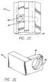
- FIGS. 1 and 2 A- 2 Ean optical assembly in accordance with a first preferred embodiment of the present invention is illustrated in perspective and component views, respectively.
- the optical assembly illustratedis a configuration employing optical components and alignment suitable for an application in a fiber optic distribution network and will also be referred to herein as an optical networking unit.
- optical networking unitmay be employed in other applications and with other optical components and configurations than those described therein or below. Therefore, the present invention is not limited to optical networking units, although such provide one preferred embodiment of the present invention.
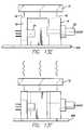
- optical assembly 10is illustrated in a perspective view.
- the embodiment of FIG. 1is an implementation employing two optical components, however, as will be described in relation to subsequent figures, the optical assembly and optical packaging method of the present invention may be employed for additional numbers of optical components, both passive and active in nature.
- the optical componentsare mounted on a substrate 12 via optical component holders 14 and 16 , respectively.
- the substrate 12is composed of a rigid transparent material which allows a desired wavelength of radiation to pass through.
- a radiation curing adhesive 18to be used to affix the optical component holders to the substrate 12 .
- a UV curing adhesiveis employed for the adhesive 18 and substrate 12 is transparent to UV light.
- a suitable UV curable adhesiveis Optocast 3400 epoxy and the corresponding wavelength of radiation is about 325 nm.
- the substratepreferably has a relatively low coefficient of thermal expansion.
- a suitable material for substrate 12is borosilicate glass.
- Other suitable rigid transparent materialsmay also be employed for transparent substrate 12 , however.
- the illustrated optical components mounted in respective optical component holders 14 , 16are an optical fiber 20 terminated in an optical fiber holder, sleeve, capillary tube, or ferrule 22 and an active optical component 24 .
- the optical component 24is illustrated configured in a cylindrical package which may be a conventional cylindrical transistor outline (TO) package or “TO can”.
- the optical component 24may be a laser diode, optical detector such as a diode photodetector, or other active optical component adapted for the particular application.
- the active componentmay also incorporate electrical circuitry or devices in a common package; for example, built-in amplification circuitry in the case of a detector or modulation circuitry in the case of a laser diode or other light source.
- the optical component holders 14 and 16are dimensioned so that the optical components are optically aligned, i.e., the holders are dimensioned such that the nominal optical axis of each of the components is configured the same distance above the top surface of the substrate 12 .
- the optical component holders 14 and 16may be composed of a suitable rigid material, such as a metal.
- a suitable rigid materialsuch as a metal.
- brassis one example of a suitable metal which might be employed for holders 14 and 16 .
- both the holders 14 and 16are composed of materials of relatively low, and closely matched, coefficients of thermal expansion to that of substrate 12 so that temperature variations will not cause the relative alignment of the components to change.
- the optical component holder 16is illustrated in FIG. 1 as having an L-shape with two mounting holes 26 and 28 which receive mounting members such as a screw. As will be described below in relation to FIG. 3, these are employed to mount the assembly to a housing and/or to a circuit board and also to thermally couple the component holder 16 to the housing to allow heat dissipation if the active component 24 is a significant heat generating component such as a laser diode or a photodetector with built-in amplifier such as a cable TV amplifier or a PIN-TIA photodetector (photodetector with built-in Trans Impedance Amplifier).
- a significant heat generating componentsuch as a laser diode or a photodetector with built-in amplifier such as a cable TV amplifier or a PIN-TIA photodetector (photodetector with built-in Trans Impedance Amplifier).
- the mounting holes 26 and 28 and the portion of the L-shape of component holder 16 containing the holesmay be dispensed with.
- the resultant shape of component holder 16is illustrated by the dashed line in FIG. 1, i.e., a simple rectangular block shape may be employed.
- Various other configurations and shapes of the optical component holder 16 and also optical component holder 14 , geared to facilitate mounting to external package or a housing, special features that enable gripping and holding during manufacturing and other featuresare also possible, however.
- the substrate 12is illustrated in a perspective view.
- the top surface 30 of the substrate 12is preferably a flat surface to facilitate the alignment of the optical component holders and optical components relative to the substrate and even bonding to the substrate.
- the substrate 12has a thickness T sufficient to provide structural rigidity to the overall assembly. For example, for a substrate material composed of glass a thickness of 50-200 mils may be suitable.
- the substrate 12is illustrated with a rectangular geometry in FIG. 2A, it should be appreciated that other geometries are also possible, for example, a cylindrical or other regular shape may be suitably employed.
- the top surface 30 of the substrate 12may be textured or roughened to enable an improved adhesive bond while maintaining transperancy to the curing radiation.
- the optical fiber 20 and ferrule 22may be conventional and the assembly of the present invention is preferably adapted to work with standardized optical fiber components. Therefore, the ferrule illustrated in FIG. 2B may have a simple generally cylindrical configuration and the fiber holder 14 has a matching suitable opening 36 . However, various other fiber and/or ferrule configurations may be employed and optical fiber holder 14 will be modified accordingly. Also, the assembly of the present invention can work with various ferrule materials, for example, ferrule 22 may be composed of glass, ceramic, metal or plastic.
- the tip of the fibermaybe extended from its sleeve or ferrule holder, angle polished or cleaved to reduce reflections with or without antireflection coating. Polishing the fiber tip after its insertion and securing in the holder 14 provides means for precise relationship of the angle polish plane to the holder.
- the diameter of the opening 36 in the optical fiber holder 14substantially corresponds to the diameter of the tip of ferrule 22 and has a slight taper in the case of a press fit mounting or slightly larger than the diameter of ferrule 22 in the case of an adhesive bonding between the ferrule and holder 14 .
- the end of the opening 36 facing the active optical component 24may be formed in an extension 34 from the body of the holder 14 .
- the extension 34can also be used during polishing of the fiber tip and/or used for securing additional components as will be explained later.
- the bottom surface 32 of the optical fiber holder 14is adapted to contact the flat surface 30 of the substrate 12 in a manner which will allow precise alignment of the optical fiber with the active component 24 and even bonding forces when the adhesive is cured. Therefore, the bottom surface 32 is either preferably flat or slightly curved with a slight curve illustrated in FIG. 2 C. As will be explained in more detail in relation to one of the preferred method of assembly of the present invention, such a slight curvature allows a slight movement during alignment from a perfectly perpendicular orientation relative to the substrate while still ensuring solid contact with the substrate and even bonding with the adhesive bonding material.
- the bonding surface 32 of the holder 14may be textured or roughened to enable an improved adhesive bond.
- the optical fiber holder 14is relatively simple in shape and easy to fabricate and therefore may be advantageously employed, it will be appreciated that such configuration is only one example of a suitable embodiment and a variety of other shapes and configurations for such holder 14 may be employed while remaining within the scope of the present invention.
- the shape of the holder 14is also appropriate for mounting into a polishing jig during its fabrication and held into a gripper or mounting platform during alignment as will be explained later.
- the active optical component 24 and optical component holder 16are illustrated in front and bottom perspective views respectively.
- Active optical component 24is illustrated in a simple cylindrical shape, which may correspond to a TO can package, and holder 16 has a matching opening 40 .
- TO can packagesare conventionally employed for many active optical components, various other configurations may be employed for the active optical component and/or it's package and active optical component holder 16 will be modified accordingly.
- the component 24is typically packaged in a metal can the optical component may be composed of various other materials, for example, glass, ceramic, or plastic.
- a lens 44 of suitable typemay also be provided as schematically illustrated.
- an aspheric, GRIN or ball lensmay be provided as part of the active device 24 .
- the diameter of the opening 40 in the active optical component holder 16substantially corresponds to the diameter of component 24 in the case of a press fit mounting or slightly larger than the diameter of component 24 in the case of an adhesive, welding or other bonding between the component 24 and holder 16 .
- the bottom surface 42 of the active optical component holder 14is adapted to contact the flat surface 30 of the substrate 12 in a manner which will allow precise alignment of the optical fiber with the active component 24 and even bonding to the substrate. Therefore, the bottom surface 42 is either preferably flat or slightly curved, with a slight curve on a portion of the bottom surface illustrated in FIG. 2 E. As will be explained in more detail in relation to the preferred method of assembly of the present invention, such a slight curvature allows a slight movement during alignment from a perfectly perpendicular orientation relative to the substrate while still ensuring solid contact with the substrate and even bonding with the adhesive bonding material.
- the bonding surface 42 of the active component 24may be textured or roughened to enable an improved adhesive bond.
- FIG. 1has been illustrated with an optical fiber and an active optical component such as a laser diode or a photodetector, it should be appreciated that other optical components may equally be provided in an optical assembly such illustrated in FIG. 1 .
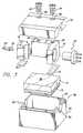
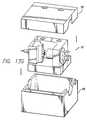
- FIG. 3an exploded view of the optical assembly of FIG. 1 configured in a housing is illustrated.
- the components of the optical assemblycorrespond to those described in relation to FIGS. 1 and 2 and like numerals are used in FIG. 3 .
- the illustrated embodiment of the housingincludes bottom and top sections 50 , 52 , respectively.
- the two sections 50 and 52mate to form a substantially sealed enclosure with the leads for active optical component 24 extending from a first opening 54 and with the optical fiber 20 extending from a second opening 56 .
- the top and bottom sections 50 and 52mate together along a mating surface 58 which may include a mating ridge 60 or other means for securely engaging the top and bottom sections.
- the active optical component holder 16is coupled to the top section 52 via screws 62 and 64 which engage mounting holes 26 and 28 in holder 16 and matching holes 66 and 68 in the top section 52 .
- Use of screws 62 and 64 to couple the active optical component holder 16 to the top section 52are preferably employed where a good thermal contact between the two structures is desired thereby allowing heat generated by the active optical component 24 to be dissipated through the housing.
- the housing materialis preferably chosen to have a good thermal conductivity and for example may be a suitable metal.
- the elongated portion of the L-shaped structure of holder 16also increases the contact area between the active optical component holder 16 and housing thereby further enhancing heat transfer into housing for dissipation into the air.
- additional heat dissipation meansmay be provided.
- a heat sinkmay be coupled to the exterior surface of the housing or directly to the active optical component 24 so as to extend from the housing to provide a larger surface for heat dissipation.
- optical component holder 16 and top section 52 of the housingmay be combined in a single piece.
- the housingneed not be composed of a metal or other good thermal conductor and a more inexpensive or easily molded material such as a plastic may be employed.
- the screws 62 and 64may also be used to couple the assembly to a circuit board or other suitable mounting structure.
- the direct coupling to the component holder 16 through the screws 62 and 64securely mounts the optics to the circuit board or other mounting surface. Vibration into the optics assembly may be further reduced by providing a cushioning layer 70 between the substrate 12 and the bottom section 50 of the housing.
- layer 70may be a caulking material, layer of rubber, or any other suitable cushioning material which may be easily introduced in manufacturing and assembly of the housing.
- the opening in the complete assembly where the fiber and the leads of the active components extend outsidemay be sealed with an appropriate silicone rubber.
- FIG. 3While a simple two-piece rectangular package is illustrated in FIG. 3 for the combined optics assembly 10 and housing, it will be appreciated that various other configurations may also be provided. Therefore, the present invention should not in any way be limited to the particular configuration or geometry illustrated in FIG. 3 and a variety of different housing structures and means of coupling to the optics assembly may be provided while remaining within the spirit and scope of the present invention.
- FIGS. 4A and 4Ba second preferred embodiment 100 of the optical assembly of the present invention is illustrated in perspective and side sectional views, respectively.
- the illustrated embodiment 100adds an additional active optical component 110 along with passive optics 112 to the embodiment of FIG. 1 .
- some of the components of the embodiment 100may correspond to those described above in relation to FIG. 1 and like numerals are used for such common components.
- the embodiment 100preferably comprises transparent substrate 12 to which are mounted the optical components via a radiation curable adhesive, as in the case of the previously described embodiment.
- the optical component 24 and optical component holder 16may be as described above in relation to the embodiment of FIG. 1 .
- the added optical component 110may preferably be any of a variety of known active optical components such as of the type described above in relation to active optical component 24 .
- active optical component 110may comprise a photodetector, a photodetector and built-in amplifier combination, such as a combined photodetector and cable TV amplifier or PIN-TIA combination, or other known active optical component.
- the second active optical component 110may preferably be provided in a conventional package such as a cylindrical TO can and the optical component holder 120 is preferably configured with an opening adapted to receive such a conventional component.
- the component holder 120is dimensioned so as to place the second active optical component 110 at the correct distance from the substrate 12 so as to be optically aligned with the optical axes of the optical fiber 20 and the first active optical component 24 .
- the holder 120is preferably a good thermal conductor such as brass and may be provided with mounting holes similar to holes 26 and 28 to thermally couple the holder 120 to a heat sink as described in relation to the holder 16 in the previously described embodiment.
- holder 120preferably has a relatively low coefficient of thermal expansion which also substantially matches that of substrate 12 and holders 16 and 114 .
- the holder 120is preferably affixed to the substrate 12 by the use of a radiation curable adhesive 18 ; for example, a UV curable adhesive as described previously may be employed, and has a flat or slightly curved lower surface for contacting the flat upper surface of substrate 12 .
- the optical fiber holder 114 of the embodiment 100may preferably be modified from the previously described optical fiber holder by the provision of a platform or extension 116 for receiving the passive optics 112 .
- the passive optics 112may be configured in a passive optics holder 118 which is mounted on a flat upper surface of platform 116 .
- passive optics 112may include a beam splitter and one or more or filters, to allow the optical path of the light beam to be provided to both the first and second active optical components 24 and 110 as well as the fiber.
- the passive optics 112may be mounted directly onto the flat surface of platform 116 .
- passive optics 112to be preconfigured relative to the optical fiber 20 and ferrule 22 prior to assembly of the component holder 114 onto the substrate 12 .
- the passive optics holder 118may alternatively be assembled directly onto substrate 12 in which case a radiation curable adhesive may be employed to adhere such holder to the substrate as in the case of the other optical component holders.
- the extension 116 of the optical fiber holder 114may be dispensed with.
- FIGS. 5A and 5Ban alternate embodiment of the optical fiber holder 114 is illustrated having a modified embodiment passive optics holder 118 .
- platform 116 of the previously described embodimentis replaced with a modified passive optics holder 118 having extensions 130 and 132 for engaging the fiber optic holder and suspending the passive optics in the optical path.
- the extensions 130 and 132engage matching slots 134 and 136 in the fiber optic holder 114 and the may be secured therein through any of a number of known techniques such as epoxy bonding, laser welding, or other known techniques.
- the passive optics holder and mounting techniqueis designed to facilitate the alignment and assembly of the passive optics relative to the optical fiber. It will be appreciated by those skilled in the art that other configurations are equally possible to provide the desired relation between the optical fiber and passive optical components and may vary with the particular optical components and configuration adopted for the overall assembly.
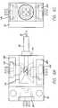
- FIGS. 6A-6Da third embodiment of the optical assembly of the present invention is illustrated employing four optical components, for example, three active optical components and an optical fiber, in a single compact optical assembly.
- the optical fiber, first active optical component, second active optical component and the substratemay generally correspond to the previously described embodiments and the discussion thereof applies to the present embodiment as well and is incorporated by reference. Accordingly, like numerals will be employed and a detailed discussion of these elements will not be provided for brevity.
- the assembly 200differs from the preceding embodiment by the addition of a fourth optical component which may be a third active optical component 210 in a preferred embodiment for an optical networking application.
- Third active optical componentmay be any of a variety of known active optical components such as of the type described above in relation to active optical component 24 .
- active optical component 210may comprise a photodetector, a photodetector and built-in amplifier combination, such as a combined photodetector and cable TV amplifier or PIN-TIA combination, or other known active optical component.
- the third active optical component 210may preferably be provided in a conventional package such as a cylindrical TO can and the third active optical component holder 220 is preferably configured with an opening adapted to receive such a conventional component.
- the component holder 220is dimensioned so as to place the third active optical component at the correct distance from the substrate 12 so as to be optically aligned with the optical axes of the optical fiber 20 and the first and second active optical components 24 and 110 .
- the holder 220may be provided with mounting holes similar to holes 26 and 28 to thermally couple the holder 220 to a housing or heat sink as described in relation to the holder 16 in the previously described embodiment.
- holder 220preferably has a relatively low coefficient of thermal expansion which also substantially matches that of substrate 12 .
- the holder 220is preferably affixed to the substrate 12 by the use of a radiation curable adhesive, for example, a UV curable adhesive as described previously may be employed, and has a flat or slightly curved lower surface for contacting the flat upper surface of substrate 12 .
- passive optics 112are preferably provided to direct the light beam to the various optical components. These passive optics may be provided in a holder 118 or mounted directly on extension 116 of fiber optic holder 114 , as described previously. If provided in a holder 118 , such holder may be mounted to the fiber holder or directly on substrate 12 .
- the choice of passive optical components and their configuration, both relative to each other and the fiber,may be selected for the specific implementation using criteria well known in the art. For example, the relative configuration is chosen generally to avoid undesired reflections as is well known in the art.
- the passive optics holder 118may comprise a block 230 of a suitable rigid material having a coefficient of thermal expansion matching the fiber optic component holder 114 .
- the passive optics holder 118preferably has a flat upper surface and includes mounting and alignment recesses 232 and 234 for receiving optical filters 236 and 238 therein.
- a wedge shaped extension 240in turn is provided which has first and second angled flat surfaces for receiving and aligning beam splitters 242 and 246 .
- the wedge and recess locationsare configured such the beam of light is directed to the active optical components and fiber with a minimum of undesired reflections and beam loss.
- the specific optical filters and beam splitters employedwill vary with the particular application and may be conventional in nature.
- the bottom surface of block 230preferably its flat to engage the upper flat surface of extension 116 of the fiber optic component holder 114 .
- the block 230may preferably be flat or slightly curved to mate with the upper flat surface of the substrate 12 , for reasons described in relation to the other optical component holders.
- the holder 118preferably will be mounted to substrate 12 via a radiation curable adhesive on the bottom surface thereof.
- the alignment configuration recesses and surfaces of holder 118 in FIG. 7may be incorporated in the platform 116 of the fiber holder described previously in an embodiment where the passive optics are mounted directly on the fiber holder.
- the passive optics assemblymay be mounted on the active optical component holder 16 instead of the fiber holder and the holder 16 may be modified accordingly. Also, the passive optical components may be split into two separate assemblies with one mounted on the fiber holder and one mounted on the active optical component holder. Alternatively, one passive optical component assembly may be mounted on the substrate and the other on holder 114 or 16 .
- the particular illustrated passive optics in FIG. 8correspond to suitable passive optics for a three active component embodiment of the optical assembly such as described in relation to FIGS. 6A-6D.
- One specific implementation of the optics for such a three active component embodimentwill be described below in relation to FIG. 9 .
- a single beam splitter and single optical filtermay be employed and the corresponding modifications in the passive optics holder 118 will be apparent to those skilled in the art.
- the configuration illustrated in FIG. 9may correspond to a data diplexer or duplexer.
- additional or different passive optical componentsmay be provided on holder 118 and such modifications will also be apparent to those skilled in the art.
- FIG. 9one preferred implementation of the optics for a four optical component embodiment corresponding to three active optical components and an optical fiber is illustrated in a schematic drawing. Like numerals for components described in the preceding embodiments will be employed for the optical components of FIG. 9 .
- the specific implementation of FIG. 9is suited for implementation as an optical networking unit and implementation in a fiber optic data distribution network is one preferred application thereof.
- a laser diode source 24corresponds to a first active optical component and provides a laser light at a first wavelength ⁇ 1 .
- ⁇ 1may lie in the range of 1280-1380 nm.
- the light provided by the laser diode 24will be modulated with data and provided to the optical fiber 20 for transmission along the fiber optic network as shown by the first beam path.
- Modulated laser light at a second wavelength ⁇ 2in turn is received into the optical networking unit from optical fiber 20 , as indicated by the second beam path, and passed to the first photodetector 110 corresponding to the second active optical component in the assembly described above. This incoming light is directed to the detector 110 by beam splitter 244 .
- ⁇ 2may lie in the range of 1440-1500 nm.
- Beam splitter 244may be for example a dichroic beam splitter of a type well known to those skilled in the art. Light at other wavelengths than ⁇ 2 are blocked from detector 110 by filter 238 .
- a third wavelength of laser light ⁇ 3may also be received from the optical fiber 20 and provided to a second photodetector 210 , corresponding to the third active optical component in the assembly described above.
- ⁇ 3may lie in the range of 1520-1600 nm. This third wavelength of light is provided to detector 210 by second beam splitter 242 .
- Beam splitter 242may also be for example a dichroic beam splitter of a type well known to those skilled in the art.
- the other wavelengths of light present in the optical assemblyare blocked by second filter 236 .
- first and second optical absorbers 246 , 248may be provided as indicated in FIG. 9 .
- the optical absorbersmay comprise antireflective or absorptive coatings on appropriate inner surfaces of the optical component holders and/or the housing of the optical assembly at locations where the light may be directed from the beam splitters.
- an antireflective coating 250may be provided on the surface of optical fiber 20 as schematically illustrated in FIG. 9 .
- the optical assembly of FIG. 9is illustrated with various additional configurations of passive optical elements which may be provided in the implementation of the optics of FIG. 9 .
- lensesmay be provided in various configurations in the optical assembly.
- suitable lensescan be GRIN, ball, aspheric, etc.
- FIG. 10two possible lens configurations are illustrated for each active optical element, on opposite sides of the corresponding filter.
- the mounting approach adopted for the lensesmay also be varied, for example, the lenses may be part of the active optical component package, mounted on the component holders, or mounted on one or more passive optical component holders in the beam path.
- the passive optical component holder or holdersin turn may be mounted on the fiber holder, active component holder or directly on the substrate.
- a suitable passive optical component holder which may incorporate a lensis illustrated in FIG. 11 described below.
- optical fibermay have a lens 252 which may be affixed to the end of the ferrule, mounted to the fiber holder, or mounted on a passive optical component holder.
- the passive optical component holderin turn may be mounted on the fiber holder or directly on the substrate.
- Laser diode 24also has an associated lens which may be incorporated in the diode package as lens 44 as has been described previously or may be configured on the laser diode holder or on a passive optical component holder, as indicated by lens 262 .
- the passive optical component holdermay be mounted on the fiber holder as described previously or on the laser diode holder as illustrated by passive optical component holder 266 in FIG. 10 .
- the passive optical component holder 266may also be mounted directly on the substrate. Holder 266 may be a common holder incorporating some or all of the other passive optical components or may be a separate holder incorporating lens 262 and/or selected other passive optical components. As also illustrated in FIG. 10 an optical isolator 264 may be provided in the beam path of laser diode 24 . Optical isolator may be mounted on holder 266 or directly on the laser diode holder.
- a lens 256 or 260is associated with first photodetector 110 , corresponding to the second active optical component in the assembly described above.
- Lens 256is configured on the photodetector side of the filter 238 whereas lens 260 is on the opposite side of the filter.
- the selection of the position of the lensmay depend on a variety of factors including the specific application, cost and space constraints, and the component packaging.
- Lens 256may be incorporated in the photodetector package, mounted on the photodetector holder or on a passive component holder.
- Lens 260may preferably be mounted on a passive component holder.
- the configuration with lens 260may incorporate filter 238 in the photodetector package or on the passive component holder.
- a lens 254 or 258is associated with second photodetector 210 , corresponding to the third active optical component in the assembly described above.
- Lens 254is configured on the photodetector side of the filter 236 whereas lens 258 is on the opposite side of the filter.
- the selection of the position of the lensmay depend on a variety of factors including the specific application, cost and space constraints, and the component packaging, however, the selection need not be the same for the two photodetectors.
- Lens 254similarly may be incorporated in the photodetector package, mounted on the photodetector holder or on a passive component holder.
- Lens 258may also preferably be mounted on the passive component holder and filter 238 may be incorporated in the photodetector package or mounted on the passive component holder.
- FIGS. 9 and 10It will be appreciated from comparison of the schematic drawings of FIGS. 9 and 10 with the preceding discussion of the preferred structural embodiments of the optical assembly of the present invention that a very compact implementation of the optical assembly of FIGS. 9 and 10 may be provided.
- the modular nature of the componentsenable easier configuration changes as compared with solid housing approaches.
- FIGS. 9 and 10the embodiment described previously with two active optical components and an optical fiber may effectively implement a bidirectional optical networking unit with a diode laser operating at a first wavelength ⁇ 1 and a photodetector detecting a second wavelength ⁇ 2 , and such an optical networking unit is implied herein from FIGS. 9 and 10 (merely corresponding to the absence of second detector 210 and associated passive optics in the figures).
- one active optical componenteither a laser or photodetector, operating at a wavelength ⁇ 1 and an optical fiber may equally be very effectively implemented in the compact assembly of the present invention and such an optical networking unit is also implied herein.
- two or more of ⁇ 1 , ⁇ 2 , and ⁇ 3may be equal.
- the corresponding beam splitterwill be a power splitting beam splitter as known in the art.
- implementing the optical assembly for a particular application and particular selection of opticsmay involve a variety of modifications from the preceding preferred embodiments and such modifications are within the spirit and scope of the present invention.
- FIG. 11a passive optics assembly 270 incorporating a lens, in accordance with an alternate embodiment of the present invention is illustrated in a perspective view.
- the passive optics assembly of FIG. 11may be advantageously employed with a configuration having a lens on the opposite side of a filter from a photodetector, or other active optical component, such as described above in relation to FIG. 10 .
- filter 238 and lens 260 in FIG. 11are given the same reference numerals as in FIG. 10 . Nonetheless it should be appreciated that the assembly of FIG. 11 may also be employed for lens 258 , 262 or 252 described in FIG. 10, or for a combination of two or more of these lenses.
- the passive optics assembly 270may comprise a block 272 of a suitable rigid material having a coefficient of thermal expansion matching the component holder to which it will be mounted.
- the block 272preferably has a flat upper surface and includes a mounting and alignment recess for receiving optical filter 238 therein.
- a wedge shaped extension 276in turn is provided which has first and second angled flat surfaces for receiving and aligning beam splitters 242 and 244 .
- the bottom surface of block 272preferably is configured to engage the active optical component to which it is mounted.
- the block 272may preferably be flat or slightly curved and may be textured or roughened to enable an improved adhesive bond to mate with the upper flat surface of the substrate 12 , for reasons described in relation to the other optical component holders.
- the block 272preferably will be mounted to substrate 12 via a radiation curable adhesive on the bottom surface thereof.
- a lens mounting extension 274preferably integrally formed as part of block 272 , is also provided.
- a front surface thereofreceives lens 260 which may be epoxy bonded or otherwise affixed to extension 274 .
- a cylindrical opening 278is provided in extension 274 to allow the laser light therethrough.
- a rear surface of extension 274may receive filter 238 aligned with the circular opening 278 .
- filter 238may be incorporated in the photodetector package or may be mounted on the photodetector holder.
- a variety of modifications of the assembly 270such as to add additional lenses, may be made and will be apparent to those skilled in the art.
- a laser diode source 24provides laser light at a first wavelength ⁇ 1 .
- ⁇ 1may lie in the range of 1250-1380 nm.
- Laser diode 24may incorporate a lens 44 as illustrated, or alternate lens configurations such as discussed above may be provided.
- the light provided by the laser diode 24will be modulated with data and provided to the optical fiber 20 for transmission along the fiber optic network as shown by the first beam path.
- Modulated laser light at a second wavelength ⁇ 2in turn is received into the optical networking unit from optical fiber 20 , as indicated by the second beam path, and passed to photodetector 110 .
- Photodetector 110may include lens 256 or the other lens configurations described above may be provided.
- the incoming light from fiber 20is directed to the detector 110 by beam splitter 244 .
- ⁇ 2may lie in the range of 1440-1500 nm.
- Light at other wavelengths than ⁇ 2are blocked from detector 110 by filter 238 .
- a third wavelength of laser light ⁇ 3may also be received from a second optical fiber 280 and provided to first optical fiber 20 .
- ⁇ 3may lie in the range of 1520-1600 nm.
- Fiber 280may include a lens 282 and a lens may similarly be provided on fiber 20 as has been described in previous embodiments.
- the other wavelengths of light present in the light transmitted by optical fiber 20 and LD source 24 scattered on beam splitter 242 or other stray light in the unitare blocked by second filter 236 .
- first and second optical absorbers 246 , 248may be provided.
- the optical absorbersmay comprise antireflective or absorptive coatings on appropriate inner surfaces of the optical component holders and/or the housing of the optical assembly at locations where the light may be directed from the beam splitters.
- an antireflective coating 250may be provided on the surface of optical fiber 20 and/or fiber 280 .
- FIGS. 9, 10 and 12are possible within the scope of the present invention.
- additional optical componentsmay be added, along with beam splitters, in a cascaded manner which is apparent from the illustrated embodiments.
- Various combinations of active optical components and fibersare possible in such additional embodiments.
- Various additional passive optical componentsincluding lenses, beam splitters, filters, prisms, and optical isolators may also be provided.
- a first act 300 in the method of present inventionis the assembly of the optical components in their respective holders and the securing of the components in place in the holders.
- the act of inserting and securing the optical component in the corresponding holdermay simply comprise inserting the component in the corresponding matching opening which is dimensioned so as to provide a relatively close fit with the optical component.
- the securing of the component to the holdermay simply be provided by a press fit to the holder. Otherwise, the inserting of the optical component into the holder is followed by a bonding or other securing act such as laser welding, epoxy bonding or other known technique for securing such components. If angled termination of the fiber is required the polishing can take place after insertion and securing the ferrule 22 inside the holder 14 .
- the passive opticsare first secured in the passive optics holder and then the holder is positioned on the extension of the optical fiber holder as illustrated in FIG. 13 C. The passive optics holder is then secured through bonding, laser welding or other known technique. Alternatively, the passive optics is positioned and secured directly on the fiber optic holder, e.g., on a platform 116 .
- This assembling and securing the optical components with the corresponding holderis repeated for as many active or passive optical components as are present in the final assembly.
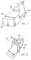
- the next act 310 in the method of the present inventioncomprises preconfiguring the optical components and holders on an alignment platform or other suitable alignment fixture.
- FIG. 13Din a top view which illustrates active optical component holder 16 configured on an alignment platform 400 with optical fiber holder 14 held in a fixed position by a suitable fixture 410 , illustrated by opposed gripping arms 410 in FIG. 13 D.
- the alignment platform 400is movable relative to the fixture 410 and is coupled to an appropriate positioning machine via arm 420 .
- a suitable positioning machineis commercially available from Burleigh Instruments, Inc., model Freedom 1000.
- platform 400is movable in at least one direction but preferably additional degrees of movement are also provided.
- two, three, four, five or six degrees of freedom positioningmay be provided. This may include pivoting degrees of motion for the platform as well as motion in the plane and perpendicular to the plane of the view of FIG. 13 D.
- the optical elementsare preconfigured relative to each other on the platform 400 and the grips 410 so that the optical axis of the two elements are approximately in alignment. For example, this may be done manually or by moving the alignment platform 400 to a preset position.
- the next act 320 in the method of the present inventioninvolves more precisely aligning the optical components while the components are active.
- the active component 24is a diode laser and the other optical component an optical fiber
- the lasermay be coupled to a predetermined data/modulation source and the output from the optical fiber monitored as the alignment platform 400 is adjusted.
- the output from the optical fibershows optimal coupling between the laser and the fiber the alignment is complete.
- the active optical componentis a detector
- an input modulated laser beammay be directed into the optical fiber and the output from the detector monitored.
- the platform 400may be adjusted to alter the alignment of the two optical components until an optimal output from the detector is provided.
- the next act 330 in the method of the present inventioncomprises placing the transparent substrate 12 onto the bottom surfaces of the optical components while maintaining the position of the component holders, as illustrated in FIG. 13E in a side view.
- the bottom surfaces of the optical component holdersare coated with a suitable radiation curable adhesive 18 prior to the placing of the substrate 12 onto the optical components.
- a suitable radiation curable adhesive 18it may be deposited immediately prior to the placing of the substrate 12 onto the components or may be provided earlier in the assembly process if exposure to air for a relatively prolonged period of time will not affect the curing properties of the adhesive.
- the adhesivemay be placed on the substrate at the approximate location of the component holders prior to lowering the substrate onto the holders.
- the next act 340 in the method of the present inventioncomprises exposure of the radiation curable adhesive with radiation through the transparent substrate while the optical components are maintained in their correctly aligned position.
- This act of the method of the present inventionis illustrated in FIG. 13F in a side view. More specifically, this act of curing the adhesive by exposure through the transparent substrate preferably comprises exposing the UV curable adhesive to UV radiation and preferably the adhesive comprises a relatively low coefficient thermal expansion adhesive having low curing shrinkage. As result, the amount of distortion of the alignment of the optical components will be minimized during the curing process. As result, after the curing process is completed the optical components will be secured to the substrate 12 in their correctly aligned position.
- one or two additional active optical componentsmay be provided in an optimized alignment relative to an optical fiber by repeating the above described acts of preconfiguring the optical component relative to the fiber, optimizing the alignment of the optical component to the fiber by monitoring an output of the component while the optical component is active, and exposing adhesive on the bottom of the optical component holder with radiation provided through the transparent substrate to cure the adhesive and fix the optical component holder in place.
- the next act 350 of the method of the present inventioncomprises assembling the housing around the optical components mounted on the assembly as illustrated in FIG. 13 G.
- the act of assembling the housing around the optical assemblymay include securing the housing to the circuit board or other support 430 via mounting holes 432 and 434 as illustrated in FIG. 13 H.
- the assembled housingmay then be sealed if desired to prevent moisture or dirt from affecting the optics.
- the optical fiber and ferruleare not directly mechanically coupled to the housing to avoid mechanical stress from the housing to the fiber. Therefore, the hole in the housing surrounding the ferrule and fiber may be sealed with a soft sealant such as a silicone gel to avoid rigid coupling to the housing.
- the present inventionprovides an optimized optical assembly, which provides a compact assembly of optical components which are optimized in their relationship relative to each other. It will be further appreciated the present invention provides a method for assembling the optical components into an optimized optical assembly which may be readily implemented in a cost-effective manner.
Landscapes
- Physics & Mathematics (AREA)
- Engineering & Computer Science (AREA)
- Computer Networks & Wireless Communication (AREA)
- Signal Processing (AREA)
- Optics & Photonics (AREA)
- Electromagnetism (AREA)
- General Physics & Mathematics (AREA)
- Optical Couplings Of Light Guides (AREA)
Abstract
Description
Claims (25)
Priority Applications (5)
| Application Number | Priority Date | Filing Date | Title |
|---|---|---|---|
| US09/836,500US6652158B2 (en) | 2000-09-05 | 2001-04-17 | Optical networking unit employing optimized optical packaging |
| US09/946,740US6606430B2 (en) | 2000-09-05 | 2001-09-04 | Passive optical network with analog distribution |
| PCT/US2001/027436WO2002021183A1 (en) | 2000-09-05 | 2001-09-04 | Optical networking unit employing optimized optical packaging |
| AU2001290614AAU2001290614A1 (en) | 2000-09-05 | 2001-09-04 | Optical networking unit employing optimized optical packaging |
| TW090121856ATW517473B (en) | 2000-09-05 | 2001-09-04 | Optical networking unit employing optimized optical packaging |
Applications Claiming Priority (2)
| Application Number | Priority Date | Filing Date | Title |
|---|---|---|---|
| US23013200P | 2000-09-05 | 2000-09-05 | |
| US09/836,500US6652158B2 (en) | 2000-09-05 | 2001-04-17 | Optical networking unit employing optimized optical packaging |
Related Parent Applications (1)
| Application Number | Title | Priority Date | Filing Date |
|---|---|---|---|
| US09/907,056Continuation-In-PartUS20020027688A1 (en) | 2000-09-05 | 2001-07-17 | Fiber optic transceiver employing digital dual loop compensation |
Related Child Applications (1)
| Application Number | Title | Priority Date | Filing Date |
|---|---|---|---|
| US09/946,740Continuation-In-PartUS6606430B2 (en) | 2000-09-05 | 2001-09-04 | Passive optical network with analog distribution |
Publications (2)
| Publication Number | Publication Date |
|---|---|
| US20020028049A1 US20020028049A1 (en) | 2002-03-07 |
| US6652158B2true US6652158B2 (en) | 2003-11-25 |
Family
ID=26923952
Family Applications (1)
| Application Number | Title | Priority Date | Filing Date |
|---|---|---|---|
| US09/836,500Expired - Fee RelatedUS6652158B2 (en) | 2000-09-05 | 2001-04-17 | Optical networking unit employing optimized optical packaging |
Country Status (4)
| Country | Link |
|---|---|
| US (1) | US6652158B2 (en) |
| AU (1) | AU2001290614A1 (en) |
| TW (1) | TW517473B (en) |
| WO (1) | WO2002021183A1 (en) |
Cited By (93)
| Publication number | Priority date | Publication date | Assignee | Title |
|---|---|---|---|---|
| US20030021310A1 (en)* | 2001-07-30 | 2003-01-30 | Agilent Technologies, Inc. | Method and apparatus for cooling electronic or opto-electronic devices |
| US20030081912A1 (en)* | 2001-10-31 | 2003-05-01 | Agilent Technologies, Inc. | Optical fibre alignment device and method |
| US20040101258A1 (en)* | 2002-11-26 | 2004-05-27 | Aronson Lewis B. | Devices for reflection reduction in optical devices |
| US20040151443A1 (en)* | 2002-11-21 | 2004-08-05 | Toshio Mizue | Optical module |
| US20040208601A1 (en)* | 2002-01-24 | 2004-10-21 | Ronson Tan | Systems, methods and apparatus for bi-directional optical transceivers |
| US20040228586A1 (en)* | 2003-03-07 | 2004-11-18 | Yoshiki Kuhara | Optical module and method of manufacturing the same |
| US20040264886A1 (en)* | 2003-06-26 | 2004-12-30 | Michael Powers | Low cost package design for fiber coupled optical component |
| US20050051598A1 (en)* | 2003-09-05 | 2005-03-10 | Trebor Heminway | Solder preform for low heat stress laser solder attachment |
| US20050098790A1 (en)* | 2003-09-19 | 2005-05-12 | Kendra Gallup | Surface emitting laser package having integrated optical element and alignment post |
| US20050141806A1 (en)* | 2003-12-31 | 2005-06-30 | Vodrahalli Nagesh K. | Multiplexing and demultiplexing optical signals |
| US20050157988A1 (en)* | 2004-01-15 | 2005-07-21 | Adrian Lo | Optical module for bi-directional communication system |
| US20050180755A1 (en)* | 2004-02-13 | 2005-08-18 | Samsung Electronics Co.; Ltd | Bi-directional optical transceiver module |
| US20050185899A1 (en)* | 2004-02-23 | 2005-08-25 | Adrian Lo | Optical transceiver and optical module used in the same |
| US20050231974A1 (en)* | 2004-04-14 | 2005-10-20 | Marvin Ruffin | Multiple LED focused lighting device |
| US7021838B2 (en) | 2003-12-16 | 2006-04-04 | Matsushita Electric Industrial Co., Ltd. | Optimizing alignment of an optical fiber to an optical output port |
| US20060204177A1 (en)* | 2005-03-14 | 2006-09-14 | Matsushita Electric Industrial Co., Ltd. | Low cost, high precision multi-point optical component attachment |
| US7284913B2 (en) | 2003-07-14 | 2007-10-23 | Matsushita Electric Industrial Co., Ltd. | Integrated fiber attach pad for optical package |
| US20070295446A1 (en)* | 2006-06-09 | 2007-12-27 | 3M Innovative Properties Company | Bonding method with flowable adhesive composition |
| US7343535B2 (en) | 2002-02-06 | 2008-03-11 | Avago Technologies General Ip Dte Ltd | Embedded testing capability for integrated serializer/deserializers |
| US20080144303A1 (en)* | 2006-12-19 | 2008-06-19 | Finisar Corporation | Electromagnetic interference shield for an optoelectronic module |
| US20080145003A1 (en)* | 2006-12-19 | 2008-06-19 | Finisar Corporation | Optical connector latch assembly for an optoelectronic module |
| US20080146066A1 (en)* | 2006-12-19 | 2008-06-19 | Finisar Corporation | Latch assembly for an optoelectronic module |
| US20080145004A1 (en)* | 2006-12-19 | 2008-06-19 | Finisar Corporation | Communications device |
| US20080145006A1 (en)* | 2006-12-19 | 2008-06-19 | Finisar Corporation | Communications device |
| US20080145002A1 (en)* | 2006-12-19 | 2008-06-19 | Finisar Corporation | Optical subassembly connector block for an optoelectronic module |
| US7413917B2 (en) | 2003-09-19 | 2008-08-19 | Avago Technologies Fiber Ip Pte Ltd | Integrated optics and electronics |
| US7422929B2 (en) | 2003-09-19 | 2008-09-09 | Avago Technologies Fiber Ip Pte Ltd | Wafer-level packaging of optoelectronic devices |
| US20080298041A1 (en)* | 2007-05-31 | 2008-12-04 | Finisar Corporation | Electromagnetic radiation shield for an optical subassembly |
| US20080298752A1 (en)* | 2007-05-31 | 2008-12-04 | Finisar Corporation | Electromagnetic radiation shield for an optical subassembly |
| US7520679B2 (en) | 2003-09-19 | 2009-04-21 | Avago Technologies Fiber Ip (Singapore) Pte. Ltd. | Optical device package with turning mirror and alignment post |
| US7590354B2 (en) | 2006-06-16 | 2009-09-15 | Corning Cable Systems Llc | Redundant transponder array for a radio-over-fiber optical fiber cable |
| US20090279894A1 (en)* | 2008-05-08 | 2009-11-12 | Jin-Shan Pan | Triple wavelength bidirectional optical communication system |
| US7627250B2 (en) | 2006-08-16 | 2009-12-01 | Corning Cable Systems Llc | Radio-over-fiber transponder with a dual-band patch antenna system |
| US7787823B2 (en) | 2006-09-15 | 2010-08-31 | Corning Cable Systems Llc | Radio-over-fiber (RoF) optical fiber cable system with transponder diversity and RoF wireless picocellular system using same |
| US7848654B2 (en) | 2006-09-28 | 2010-12-07 | Corning Cable Systems Llc | Radio-over-fiber (RoF) wireless picocellular system with combined picocells |
| US20110091155A1 (en)* | 2009-10-19 | 2011-04-21 | Lockheed Martin Corporation | In-line forward/backward fiber-optic signal analyzer |
| US20110268397A1 (en)* | 2010-05-03 | 2011-11-03 | Avago Technologies Fiber Ip (Singapore) Pte. Ltd. | Protective socket for use with a parallel optical transceiver module for protecting components of the module from airborne matter |
| US8111998B2 (en) | 2007-02-06 | 2012-02-07 | Corning Cable Systems Llc | Transponder systems and methods for radio-over-fiber (RoF) wireless picocellular systems |
| US8175459B2 (en) | 2007-10-12 | 2012-05-08 | Corning Cable Systems Llc | Hybrid wireless/wired RoF transponder and hybrid RoF communication system using same |
| US8275265B2 (en) | 2010-02-15 | 2012-09-25 | Corning Cable Systems Llc | Dynamic cell bonding (DCB) for radio-over-fiber (RoF)-based networks and communication systems and related methods |
| US8548330B2 (en) | 2009-07-31 | 2013-10-01 | Corning Cable Systems Llc | Sectorization in distributed antenna systems, and related components and methods |
| US8644844B2 (en) | 2007-12-20 | 2014-02-04 | Corning Mobileaccess Ltd. | Extending outdoor location based services and applications into enclosed areas |
| US20140086537A1 (en)* | 2012-09-24 | 2014-03-27 | The Boeing Company | Optical Connector |
| US20140126861A1 (en)* | 2012-11-08 | 2014-05-08 | Hon Hai Precision Industry Co., Ltd. | Fixing device for optical fiber detection |
| US8867919B2 (en) | 2007-07-24 | 2014-10-21 | Corning Cable Systems Llc | Multi-port accumulator for radio-over-fiber (RoF) wireless picocellular systems |
| US8873585B2 (en) | 2006-12-19 | 2014-10-28 | Corning Optical Communications Wireless Ltd | Distributed antenna system for MIMO technologies |
| US9037143B2 (en) | 2010-08-16 | 2015-05-19 | Corning Optical Communications LLC | Remote antenna clusters and related systems, components, and methods supporting digital data signal propagation between remote antenna units |
| US9042732B2 (en) | 2010-05-02 | 2015-05-26 | Corning Optical Communications LLC | Providing digital data services in optical fiber-based distributed radio frequency (RF) communication systems, and related components and methods |
| US9112611B2 (en) | 2009-02-03 | 2015-08-18 | Corning Optical Communications LLC | Optical fiber-based distributed antenna systems, components, and related methods for calibration thereof |
| US20150253595A1 (en)* | 2014-03-07 | 2015-09-10 | Fujitsu Optical Components Limited | Optical module and optical modulation device |
| US9178635B2 (en) | 2014-01-03 | 2015-11-03 | Corning Optical Communications Wireless Ltd | Separation of communication signal sub-bands in distributed antenna systems (DASs) to reduce interference |
| US9184843B2 (en) | 2011-04-29 | 2015-11-10 | Corning Optical Communications LLC | Determining propagation delay of communications in distributed antenna systems, and related components, systems, and methods |
| US9219879B2 (en) | 2009-11-13 | 2015-12-22 | Corning Optical Communications LLC | Radio-over-fiber (ROF) system for protocol-independent wired and/or wireless communication |
| US9240835B2 (en) | 2011-04-29 | 2016-01-19 | Corning Optical Communications LLC | Systems, methods, and devices for increasing radio frequency (RF) power in distributed antenna systems |
| US9247543B2 (en) | 2013-07-23 | 2016-01-26 | Corning Optical Communications Wireless Ltd | Monitoring non-supported wireless spectrum within coverage areas of distributed antenna systems (DASs) |
| US20160036530A1 (en)* | 2013-03-15 | 2016-02-04 | Nec Corporation | Optical transmission/reception device, optical communication system and optical transmission/reception method |
| US9258052B2 (en) | 2012-03-30 | 2016-02-09 | Corning Optical Communications LLC | Reducing location-dependent interference in distributed antenna systems operating in multiple-input, multiple-output (MIMO) configuration, and related components, systems, and methods |
| US9325429B2 (en) | 2011-02-21 | 2016-04-26 | Corning Optical Communications LLC | Providing digital data services as electrical signals and radio-frequency (RF) communications over optical fiber in distributed communications systems, and related components and methods |
| US9357551B2 (en) | 2014-05-30 | 2016-05-31 | Corning Optical Communications Wireless Ltd | Systems and methods for simultaneous sampling of serial digital data streams from multiple analog-to-digital converters (ADCS), including in distributed antenna systems |
| US9385810B2 (en) | 2013-09-30 | 2016-07-05 | Corning Optical Communications Wireless Ltd | Connection mapping in distributed communication systems |
| US9420542B2 (en) | 2014-09-25 | 2016-08-16 | Corning Optical Communications Wireless Ltd | System-wide uplink band gain control in a distributed antenna system (DAS), based on per band gain control of remote uplink paths in remote units |
| US9429467B2 (en) | 2014-04-11 | 2016-08-30 | Lockheed Martin Corporation | System for non-contact optical-power measurement |
| US9455784B2 (en) | 2012-10-31 | 2016-09-27 | Corning Optical Communications Wireless Ltd | Deployable wireless infrastructures and methods of deploying wireless infrastructures |
| US9525472B2 (en) | 2014-07-30 | 2016-12-20 | Corning Incorporated | Reducing location-dependent destructive interference in distributed antenna systems (DASS) operating in multiple-input, multiple-output (MIMO) configuration, and related components, systems, and methods |
| US9525488B2 (en) | 2010-05-02 | 2016-12-20 | Corning Optical Communications LLC | Digital data services and/or power distribution in optical fiber-based distributed communications systems providing digital data and radio frequency (RF) communications services, and related components and methods |
| US9531452B2 (en) | 2012-11-29 | 2016-12-27 | Corning Optical Communications LLC | Hybrid intra-cell / inter-cell remote unit antenna bonding in multiple-input, multiple-output (MIMO) distributed antenna systems (DASs) |
| US20170054497A1 (en)* | 2012-12-27 | 2017-02-23 | Sergeev Sergey Nikolaevich | Method of transmitting an optical data signal via a fiber optical medium in opposite directions at the same carrier wavelength |
| US9602210B2 (en) | 2014-09-24 | 2017-03-21 | Corning Optical Communications Wireless Ltd | Flexible head-end chassis supporting automatic identification and interconnection of radio interface modules and optical interface modules in an optical fiber-based distributed antenna system (DAS) |
| US9621293B2 (en) | 2012-08-07 | 2017-04-11 | Corning Optical Communications Wireless Ltd | Distribution of time-division multiplexed (TDM) management services in a distributed antenna system, and related components, systems, and methods |
| US9647758B2 (en) | 2012-11-30 | 2017-05-09 | Corning Optical Communications Wireless Ltd | Cabling connectivity monitoring and verification |
| US9661781B2 (en) | 2013-07-31 | 2017-05-23 | Corning Optical Communications Wireless Ltd | Remote units for distributed communication systems and related installation methods and apparatuses |
| US9673904B2 (en) | 2009-02-03 | 2017-06-06 | Corning Optical Communications LLC | Optical fiber-based distributed antenna systems, components, and related methods for calibration thereof |
| US9681313B2 (en) | 2015-04-15 | 2017-06-13 | Corning Optical Communications Wireless Ltd | Optimizing remote antenna unit performance using an alternative data channel |
| US9715157B2 (en) | 2013-06-12 | 2017-07-25 | Corning Optical Communications Wireless Ltd | Voltage controlled optical directional coupler |
| US9729267B2 (en) | 2014-12-11 | 2017-08-08 | Corning Optical Communications Wireless Ltd | Multiplexing two separate optical links with the same wavelength using asymmetric combining and splitting |
| US9730228B2 (en) | 2014-08-29 | 2017-08-08 | Corning Optical Communications Wireless Ltd | Individualized gain control of remote uplink band paths in a remote unit in a distributed antenna system (DAS), based on combined uplink power level in the remote unit |
| US9775123B2 (en) | 2014-03-28 | 2017-09-26 | Corning Optical Communications Wireless Ltd. | Individualized gain control of uplink paths in remote units in a distributed antenna system (DAS) based on individual remote unit contribution to combined uplink power |
| US9807700B2 (en) | 2015-02-19 | 2017-10-31 | Corning Optical Communications Wireless Ltd | Offsetting unwanted downlink interference signals in an uplink path in a distributed antenna system (DAS) |
| US9948349B2 (en) | 2015-07-17 | 2018-04-17 | Corning Optical Communications Wireless Ltd | IOT automation and data collection system |
| US9974074B2 (en) | 2013-06-12 | 2018-05-15 | Corning Optical Communications Wireless Ltd | Time-division duplexing (TDD) in distributed communications systems, including distributed antenna systems (DASs) |
| US10096909B2 (en) | 2014-11-03 | 2018-10-09 | Corning Optical Communications Wireless Ltd. | Multi-band monopole planar antennas configured to facilitate improved radio frequency (RF) isolation in multiple-input multiple-output (MIMO) antenna arrangement |
| US10094992B2 (en)* | 2015-02-23 | 2018-10-09 | Sumitomo Electric Device Innovations, Inc. | Optical module with wavelength dividing filter passively aligned with respect to housing |
| US10110308B2 (en) | 2014-12-18 | 2018-10-23 | Corning Optical Communications Wireless Ltd | Digital interface modules (DIMs) for flexibly distributing digital and/or analog communications signals in wide-area analog distributed antenna systems (DASs) |
| US10128951B2 (en) | 2009-02-03 | 2018-11-13 | Corning Optical Communications LLC | Optical fiber-based distributed antenna systems, components, and related methods for monitoring and configuring thereof |
| US10136200B2 (en) | 2012-04-25 | 2018-11-20 | Corning Optical Communications LLC | Distributed antenna system architectures |
| US10135533B2 (en) | 2014-11-13 | 2018-11-20 | Corning Optical Communications Wireless Ltd | Analog distributed antenna systems (DASS) supporting distribution of digital communications signals interfaced from a digital signal source and analog radio frequency (RF) communications signals |
| US10187151B2 (en) | 2014-12-18 | 2019-01-22 | Corning Optical Communications Wireless Ltd | Digital-analog interface modules (DAIMs) for flexibly distributing digital and/or analog communications signals in wide-area analog distributed antenna systems (DASs) |
| US10236924B2 (en) | 2016-03-31 | 2019-03-19 | Corning Optical Communications Wireless Ltd | Reducing out-of-channel noise in a wireless distribution system (WDS) |
| US10560214B2 (en) | 2015-09-28 | 2020-02-11 | Corning Optical Communications LLC | Downlink and uplink communication path switching in a time-division duplex (TDD) distributed antenna system (DAS) |
| US10659163B2 (en) | 2014-09-25 | 2020-05-19 | Corning Optical Communications LLC | Supporting analog remote antenna units (RAUs) in digital distributed antenna systems (DASs) using analog RAU digital adaptors |
| US10917172B2 (en)* | 2017-07-14 | 2021-02-09 | Nec Corporation | Pluggable optical module, optical communication system, and control method of pluggable optical module |
| US11178609B2 (en) | 2010-10-13 | 2021-11-16 | Corning Optical Communications LLC | Power management for remote antenna units in distributed antenna systems |
| US11700530B2 (en) | 2020-09-21 | 2023-07-11 | Cogitari, Inc. | Radio frequency threat detection |
Families Citing this family (19)
| Publication number | Priority date | Publication date | Assignee | Title |
|---|---|---|---|---|
| US6213651B1 (en)* | 1999-05-26 | 2001-04-10 | E20 Communications, Inc. | Method and apparatus for vertical board construction of fiber optic transmitters, receivers and transceivers |
| US6813420B1 (en)* | 2000-09-21 | 2004-11-02 | Axsun Technologies, Inc. | Process and system for tunable filter optical train alignment |
| WO2002057823A2 (en)* | 2001-01-22 | 2002-07-25 | Civcom Devices & Systems Ltd. | Fast all-optical switches and attenuators |
| WO2004038473A1 (en)* | 2002-10-22 | 2004-05-06 | Firecomms Limited | Connection of optical waveguides to optical devices |
| TW586275B (en)* | 2002-12-10 | 2004-05-01 | Delta Electronics Inc | Optical signal transceiver module and optical path arrangement method thereof |
| JP2005202157A (en)* | 2004-01-15 | 2005-07-28 | Tdk Corp | Optical module |
| KR100640421B1 (en)* | 2004-12-28 | 2006-10-31 | 삼성전자주식회사 | Multiwavelength Optical Device Module |
| EP2115511B1 (en)* | 2007-02-08 | 2019-01-23 | Finisar Corporation | Single piece triplexer housing |
| US9011025B2 (en) | 2011-12-19 | 2015-04-21 | Avago Technologies General Ip (Singapore) Pte. Ltd. | Modified transistor outline (TO)-can assembly for use in optical communications and a method |
| CN102830469B (en)* | 2012-08-21 | 2016-03-02 | 武汉电信器件有限公司 | A kind of single-fiber bidirectional device for CSFP module |
| CN105278058B (en)* | 2012-10-25 | 2017-04-12 | 青岛海信宽带多媒体技术有限公司 | ONU (optical network unit) triplexer optical assembly with optical time domain signal reflection function |
| US20140286612A1 (en)* | 2013-03-20 | 2014-09-25 | All Best Precision Technology Co., Ltd. | Coupling device |
| EP3130275A4 (en)* | 2014-05-15 | 2017-12-06 | Olympus Corporation | Optical unit and endoscope provided with optical unit |
| US9782063B2 (en) | 2014-12-16 | 2017-10-10 | Novartis Ag | Optical coupling efficiency detection assembly and method of assembling the same |
| CN104570239B (en)* | 2014-12-30 | 2017-01-25 | 陈敏 | A single-fiber multi-directional optical component |
| US9572629B1 (en) | 2015-08-31 | 2017-02-21 | Novartis Ag | Sub-micron alignment of a monitoring fiber for optical feedback in an ophthalmic endo-illumination system |
| JP7117138B2 (en)* | 2018-04-23 | 2022-08-12 | スタンレー電気株式会社 | laser module |
| US10948669B2 (en)* | 2019-06-25 | 2021-03-16 | Prime World International Holdings Ltd. | Method of coupling optical fiber or fiber array with optical active component |
| CN113467015B (en)* | 2021-08-03 | 2023-03-21 | 新疆师范大学 | Center calibrating device of laser coupling platform |
Citations (4)
| Publication number | Priority date | Publication date | Assignee | Title |
|---|---|---|---|---|
| US5343548A (en) | 1992-12-15 | 1994-08-30 | International Business Machines Corporation | Method and apparatus for batch, active alignment of laser arrays to fiber arrays |
| US5867622A (en) | 1997-07-15 | 1999-02-02 | Kyocera Corporation | Module for optical communication |
| US6282351B1 (en)* | 1998-02-20 | 2001-08-28 | Sumitomo Electric Industries, Ltd. | Optical module and a method of fabricating the same |
| US6366720B1 (en)* | 1999-07-09 | 2002-04-02 | Chiaro Networks Ltd. | Integrated optics beam deflector assemblies utilizing side mounting blocks for precise alignment |
Family Cites Families (1)
| Publication number | Priority date | Publication date | Assignee | Title |
|---|---|---|---|---|
| JPH03164706A (en)* | 1989-11-24 | 1991-07-16 | Fujitsu Ltd | Optical module manufacturing method |
- 2001
- 2001-04-17USUS09/836,500patent/US6652158B2/ennot_activeExpired - Fee Related
- 2001-09-04TWTW090121856Apatent/TW517473B/ennot_activeIP Right Cessation
- 2001-09-04WOPCT/US2001/027436patent/WO2002021183A1/enactiveApplication Filing
- 2001-09-04AUAU2001290614Apatent/AU2001290614A1/ennot_activeAbandoned
Patent Citations (4)
| Publication number | Priority date | Publication date | Assignee | Title |
|---|---|---|---|---|
| US5343548A (en) | 1992-12-15 | 1994-08-30 | International Business Machines Corporation | Method and apparatus for batch, active alignment of laser arrays to fiber arrays |
| US5867622A (en) | 1997-07-15 | 1999-02-02 | Kyocera Corporation | Module for optical communication |
| US6282351B1 (en)* | 1998-02-20 | 2001-08-28 | Sumitomo Electric Industries, Ltd. | Optical module and a method of fabricating the same |
| US6366720B1 (en)* | 1999-07-09 | 2002-04-02 | Chiaro Networks Ltd. | Integrated optics beam deflector assemblies utilizing side mounting blocks for precise alignment |
Cited By (174)
| Publication number | Priority date | Publication date | Assignee | Title |
|---|---|---|---|---|
| US20030021310A1 (en)* | 2001-07-30 | 2003-01-30 | Agilent Technologies, Inc. | Method and apparatus for cooling electronic or opto-electronic devices |
| US6910811B2 (en)* | 2001-10-31 | 2005-06-28 | Agilent Technologies, Inc. | Optical fiber alignment device and method |
| US20030081912A1 (en)* | 2001-10-31 | 2003-05-01 | Agilent Technologies, Inc. | Optical fibre alignment device and method |
| US20040208601A1 (en)* | 2002-01-24 | 2004-10-21 | Ronson Tan | Systems, methods and apparatus for bi-directional optical transceivers |
| US6954592B2 (en) | 2002-01-24 | 2005-10-11 | Jds Uniphase Corporation | Systems, methods and apparatus for bi-directional optical transceivers |
| US7343535B2 (en) | 2002-02-06 | 2008-03-11 | Avago Technologies General Ip Dte Ltd | Embedded testing capability for integrated serializer/deserializers |
| US7121743B2 (en)* | 2002-11-21 | 2006-10-17 | Sumitomo Electric Industries, Ltd. | Optical module |
| US20040151443A1 (en)* | 2002-11-21 | 2004-08-05 | Toshio Mizue | Optical module |
| WO2004049015A3 (en)* | 2002-11-26 | 2005-04-28 | Finisar Corp Llc | Devices for reflection reduction in optical devices |
| US20040101258A1 (en)* | 2002-11-26 | 2004-05-27 | Aronson Lewis B. | Devices for reflection reduction in optical devices |
| US7354201B2 (en)* | 2002-11-26 | 2008-04-08 | Finisar Corporation | Devices for reflection reduction in optical devices |
| US6948865B2 (en)* | 2003-03-07 | 2005-09-27 | Sumitomo Electric Industries, Ltd. | Optical module and method of manufacturing the same |
| US20040228586A1 (en)* | 2003-03-07 | 2004-11-18 | Yoshiki Kuhara | Optical module and method of manufacturing the same |
| US20040264886A1 (en)* | 2003-06-26 | 2004-12-30 | Michael Powers | Low cost package design for fiber coupled optical component |
| US6883978B2 (en)* | 2003-06-26 | 2005-04-26 | Matsushita Electric Industrial Co., Ltd. | Low cost package design for fiber coupled optical component |
| US7284913B2 (en) | 2003-07-14 | 2007-10-23 | Matsushita Electric Industrial Co., Ltd. | Integrated fiber attach pad for optical package |
| US20050051598A1 (en)* | 2003-09-05 | 2005-03-10 | Trebor Heminway | Solder preform for low heat stress laser solder attachment |
| US7410088B2 (en) | 2003-09-05 | 2008-08-12 | Matsushita Electric Industrial, Co., Ltd. | Solder preform for low heat stress laser solder attachment |
| US20050098790A1 (en)* | 2003-09-19 | 2005-05-12 | Kendra Gallup | Surface emitting laser package having integrated optical element and alignment post |
| US7422929B2 (en) | 2003-09-19 | 2008-09-09 | Avago Technologies Fiber Ip Pte Ltd | Wafer-level packaging of optoelectronic devices |
| US7413917B2 (en) | 2003-09-19 | 2008-08-19 | Avago Technologies Fiber Ip Pte Ltd | Integrated optics and electronics |
| US7520679B2 (en) | 2003-09-19 | 2009-04-21 | Avago Technologies Fiber Ip (Singapore) Pte. Ltd. | Optical device package with turning mirror and alignment post |
| US7358109B2 (en) | 2003-09-19 | 2008-04-15 | Avago Technologies Fiber Ip (Singapore) Pte. Ltd. | Surface emitting laser package having integrated optical element and alignment post |
| US7021838B2 (en) | 2003-12-16 | 2006-04-04 | Matsushita Electric Industrial Co., Ltd. | Optimizing alignment of an optical fiber to an optical output port |
| US20050141806A1 (en)* | 2003-12-31 | 2005-06-30 | Vodrahalli Nagesh K. | Multiplexing and demultiplexing optical signals |
| US7125174B2 (en)* | 2004-01-15 | 2006-10-24 | Tdk Corporation | Optical module for bi-directional communication system |
| US20050157988A1 (en)* | 2004-01-15 | 2005-07-21 | Adrian Lo | Optical module for bi-directional communication system |
| US20050180755A1 (en)* | 2004-02-13 | 2005-08-18 | Samsung Electronics Co.; Ltd | Bi-directional optical transceiver module |
| US7369776B2 (en)* | 2004-02-13 | 2008-05-06 | Samsung Electronics Co., Ltd. | Bi-directional optical transceiver module |
| US20050185899A1 (en)* | 2004-02-23 | 2005-08-25 | Adrian Lo | Optical transceiver and optical module used in the same |
| US7048451B2 (en)* | 2004-02-23 | 2006-05-23 | Tdk Corporation | Optical transceiver and optical module used in the same |
| US7182496B2 (en) | 2004-04-14 | 2007-02-27 | Opto Technology, Inc. | Multiple LED focused lighting device |
| US20050231974A1 (en)* | 2004-04-14 | 2005-10-20 | Marvin Ruffin | Multiple LED focused lighting device |
| WO2005103559A3 (en)* | 2004-04-14 | 2006-04-20 | Opto Technology Inc | Multiple led focused lighting device |
| US20060204177A1 (en)* | 2005-03-14 | 2006-09-14 | Matsushita Electric Industrial Co., Ltd. | Low cost, high precision multi-point optical component attachment |
| US7263260B2 (en) | 2005-03-14 | 2007-08-28 | Matsushita Electric Industrial Co., Ltd. | Low cost, high precision multi-point optical component attachment |
| US7491287B2 (en) | 2006-06-09 | 2009-02-17 | 3M Innovative Properties Company | Bonding method with flowable adhesive composition |
| US20070295446A1 (en)* | 2006-06-09 | 2007-12-27 | 3M Innovative Properties Company | Bonding method with flowable adhesive composition |
| US7590354B2 (en) | 2006-06-16 | 2009-09-15 | Corning Cable Systems Llc | Redundant transponder array for a radio-over-fiber optical fiber cable |
| US7627250B2 (en) | 2006-08-16 | 2009-12-01 | Corning Cable Systems Llc | Radio-over-fiber transponder with a dual-band patch antenna system |
| US7787823B2 (en) | 2006-09-15 | 2010-08-31 | Corning Cable Systems Llc | Radio-over-fiber (RoF) optical fiber cable system with transponder diversity and RoF wireless picocellular system using same |
| US7848654B2 (en) | 2006-09-28 | 2010-12-07 | Corning Cable Systems Llc | Radio-over-fiber (RoF) wireless picocellular system with combined picocells |
| US7845862B2 (en)* | 2006-12-19 | 2010-12-07 | Finisar Corporation | Communications device |
| US7646615B2 (en) | 2006-12-19 | 2010-01-12 | Finisar Corporation | Electromagnetic inferference shield for an optoelectronic module |
| US7484987B2 (en) | 2006-12-19 | 2009-02-03 | Finisar Corporation | Latch assembly for an optoelectronic module |
| US8873585B2 (en) | 2006-12-19 | 2014-10-28 | Corning Optical Communications Wireless Ltd | Distributed antenna system for MIMO technologies |
| US20080145002A1 (en)* | 2006-12-19 | 2008-06-19 | Finisar Corporation | Optical subassembly connector block for an optoelectronic module |
| US7543995B2 (en) | 2006-12-19 | 2009-06-09 | Finisar Corporation | Optical subassembly connector block for an optoelectronic module |
| US7547149B2 (en) | 2006-12-19 | 2009-06-16 | Finisar Corporation | Optical connector latch assembly for an optoelectronic module |
| US20080145006A1 (en)* | 2006-12-19 | 2008-06-19 | Finisar Corporation | Communications device |
| US9130613B2 (en) | 2006-12-19 | 2015-09-08 | Corning Optical Communications Wireless Ltd | Distributed antenna system for MIMO technologies |
| US20080145004A1 (en)* | 2006-12-19 | 2008-06-19 | Finisar Corporation | Communications device |
| US7625137B2 (en) | 2006-12-19 | 2009-12-01 | Finisar Corporation | Communications device |
| US20080145003A1 (en)* | 2006-12-19 | 2008-06-19 | Finisar Corporation | Optical connector latch assembly for an optoelectronic module |
| US20080144303A1 (en)* | 2006-12-19 | 2008-06-19 | Finisar Corporation | Electromagnetic interference shield for an optoelectronic module |
| US20080146066A1 (en)* | 2006-12-19 | 2008-06-19 | Finisar Corporation | Latch assembly for an optoelectronic module |
| US8111998B2 (en) | 2007-02-06 | 2012-02-07 | Corning Cable Systems Llc | Transponder systems and methods for radio-over-fiber (RoF) wireless picocellular systems |
| US7762729B2 (en)* | 2007-05-31 | 2010-07-27 | Finisar Corporation | Electromagnetic radiation shield for an optical subassembly |
| US7731431B2 (en)* | 2007-05-31 | 2010-06-08 | Finisar Corporation | Electromagnetic radiation shield for an optical subassembly |
| US20080298752A1 (en)* | 2007-05-31 | 2008-12-04 | Finisar Corporation | Electromagnetic radiation shield for an optical subassembly |
| US20080298041A1 (en)* | 2007-05-31 | 2008-12-04 | Finisar Corporation | Electromagnetic radiation shield for an optical subassembly |
| US8867919B2 (en) | 2007-07-24 | 2014-10-21 | Corning Cable Systems Llc | Multi-port accumulator for radio-over-fiber (RoF) wireless picocellular systems |
| US8175459B2 (en) | 2007-10-12 | 2012-05-08 | Corning Cable Systems Llc | Hybrid wireless/wired RoF transponder and hybrid RoF communication system using same |
| US8718478B2 (en) | 2007-10-12 | 2014-05-06 | Corning Cable Systems Llc | Hybrid wireless/wired RoF transponder and hybrid RoF communication system using same |
| US8644844B2 (en) | 2007-12-20 | 2014-02-04 | Corning Mobileaccess Ltd. | Extending outdoor location based services and applications into enclosed areas |
| US20090279894A1 (en)* | 2008-05-08 | 2009-11-12 | Jin-Shan Pan | Triple wavelength bidirectional optical communication system |
| US9112611B2 (en) | 2009-02-03 | 2015-08-18 | Corning Optical Communications LLC | Optical fiber-based distributed antenna systems, components, and related methods for calibration thereof |
| US10128951B2 (en) | 2009-02-03 | 2018-11-13 | Corning Optical Communications LLC | Optical fiber-based distributed antenna systems, components, and related methods for monitoring and configuring thereof |
| US10153841B2 (en) | 2009-02-03 | 2018-12-11 | Corning Optical Communications LLC | Optical fiber-based distributed antenna systems, components, and related methods for calibration thereof |
| US9673904B2 (en) | 2009-02-03 | 2017-06-06 | Corning Optical Communications LLC | Optical fiber-based distributed antenna systems, components, and related methods for calibration thereof |
| US9900097B2 (en) | 2009-02-03 | 2018-02-20 | Corning Optical Communications LLC | Optical fiber-based distributed antenna systems, components, and related methods for calibration thereof |
| US8548330B2 (en) | 2009-07-31 | 2013-10-01 | Corning Cable Systems Llc | Sectorization in distributed antenna systems, and related components and methods |
| US20110091155A1 (en)* | 2009-10-19 | 2011-04-21 | Lockheed Martin Corporation | In-line forward/backward fiber-optic signal analyzer |
| US8755649B2 (en) | 2009-10-19 | 2014-06-17 | Lockheed Martin Corporation | In-line forward/backward fiber-optic signal analyzer |
| US9729238B2 (en) | 2009-11-13 | 2017-08-08 | Corning Optical Communications LLC | Radio-over-fiber (ROF) system for protocol-independent wired and/or wireless communication |
| US9485022B2 (en) | 2009-11-13 | 2016-11-01 | Corning Optical Communications LLC | Radio-over-fiber (ROF) system for protocol-independent wired and/or wireless communication |
| US9219879B2 (en) | 2009-11-13 | 2015-12-22 | Corning Optical Communications LLC | Radio-over-fiber (ROF) system for protocol-independent wired and/or wireless communication |
| US8275265B2 (en) | 2010-02-15 | 2012-09-25 | Corning Cable Systems Llc | Dynamic cell bonding (DCB) for radio-over-fiber (RoF)-based networks and communication systems and related methods |
| US8831428B2 (en) | 2010-02-15 | 2014-09-09 | Corning Optical Communications LLC | Dynamic cell bonding (DCB) for radio-over-fiber (RoF)-based networks and communication systems and related methods |
| US9319138B2 (en) | 2010-02-15 | 2016-04-19 | Corning Optical Communications LLC | Dynamic cell bonding (DCB) for radio-over-fiber (RoF)-based networks and communication systems and related methods |
| US9270374B2 (en) | 2010-05-02 | 2016-02-23 | Corning Optical Communications LLC | Providing digital data services in optical fiber-based distributed radio frequency (RF) communications systems, and related components and methods |
| US9853732B2 (en) | 2010-05-02 | 2017-12-26 | Corning Optical Communications LLC | Digital data services and/or power distribution in optical fiber-based distributed communications systems providing digital data and radio frequency (RF) communications services, and related components and methods |
| US9042732B2 (en) | 2010-05-02 | 2015-05-26 | Corning Optical Communications LLC | Providing digital data services in optical fiber-based distributed radio frequency (RF) communication systems, and related components and methods |
| US9525488B2 (en) | 2010-05-02 | 2016-12-20 | Corning Optical Communications LLC | Digital data services and/or power distribution in optical fiber-based distributed communications systems providing digital data and radio frequency (RF) communications services, and related components and methods |
| US20110268397A1 (en)* | 2010-05-03 | 2011-11-03 | Avago Technologies Fiber Ip (Singapore) Pte. Ltd. | Protective socket for use with a parallel optical transceiver module for protecting components of the module from airborne matter |
| US8414309B2 (en)* | 2010-05-03 | 2013-04-09 | Avago Technologies Fiber Ip (Singapore) Pte. Ltd | Receptacle for an optical transceiver module for protecting the module from airborne particles |
| US9037143B2 (en) | 2010-08-16 | 2015-05-19 | Corning Optical Communications LLC | Remote antenna clusters and related systems, components, and methods supporting digital data signal propagation between remote antenna units |
| US10014944B2 (en) | 2010-08-16 | 2018-07-03 | Corning Optical Communications LLC | Remote antenna clusters and related systems, components, and methods supporting digital data signal propagation between remote antenna units |
| US11224014B2 (en) | 2010-10-13 | 2022-01-11 | Corning Optical Communications LLC | Power management for remote antenna units in distributed antenna systems |
| US11212745B2 (en) | 2010-10-13 | 2021-12-28 | Corning Optical Communications LLC | Power management for remote antenna units in distributed antenna systems |
| US11178609B2 (en) | 2010-10-13 | 2021-11-16 | Corning Optical Communications LLC | Power management for remote antenna units in distributed antenna systems |
| US11671914B2 (en) | 2010-10-13 | 2023-06-06 | Corning Optical Communications LLC | Power management for remote antenna units in distributed antenna systems |
| US8913892B2 (en) | 2010-10-28 | 2014-12-16 | Coring Optical Communications LLC | Sectorization in distributed antenna systems, and related components and methods |
| US9325429B2 (en) | 2011-02-21 | 2016-04-26 | Corning Optical Communications LLC | Providing digital data services as electrical signals and radio-frequency (RF) communications over optical fiber in distributed communications systems, and related components and methods |
| US10205538B2 (en) | 2011-02-21 | 2019-02-12 | Corning Optical Communications LLC | Providing digital data services as electrical signals and radio-frequency (RF) communications over optical fiber in distributed communications systems, and related components and methods |
| US9813164B2 (en) | 2011-02-21 | 2017-11-07 | Corning Optical Communications LLC | Providing digital data services as electrical signals and radio-frequency (RF) communications over optical fiber in distributed communications systems, and related components and methods |
| US9184843B2 (en) | 2011-04-29 | 2015-11-10 | Corning Optical Communications LLC | Determining propagation delay of communications in distributed antenna systems, and related components, systems, and methods |
| US9807722B2 (en) | 2011-04-29 | 2017-10-31 | Corning Optical Communications LLC | Determining propagation delay of communications in distributed antenna systems, and related components, systems, and methods |
| US9369222B2 (en) | 2011-04-29 | 2016-06-14 | Corning Optical Communications LLC | Determining propagation delay of communications in distributed antenna systems, and related components, systems, and methods |
| US10148347B2 (en) | 2011-04-29 | 2018-12-04 | Corning Optical Communications LLC | Systems, methods, and devices for increasing radio frequency (RF) power in distributed antenna systems |
| US9240835B2 (en) | 2011-04-29 | 2016-01-19 | Corning Optical Communications LLC | Systems, methods, and devices for increasing radio frequency (RF) power in distributed antenna systems |
| US9806797B2 (en) | 2011-04-29 | 2017-10-31 | Corning Optical Communications LLC | Systems, methods, and devices for increasing radio frequency (RF) power in distributed antenna systems |
| US9258052B2 (en) | 2012-03-30 | 2016-02-09 | Corning Optical Communications LLC | Reducing location-dependent interference in distributed antenna systems operating in multiple-input, multiple-output (MIMO) configuration, and related components, systems, and methods |
| US9813127B2 (en) | 2012-03-30 | 2017-11-07 | Corning Optical Communications LLC | Reducing location-dependent interference in distributed antenna systems operating in multiple-input, multiple-output (MIMO) configuration, and related components, systems, and methods |
| US10136200B2 (en) | 2012-04-25 | 2018-11-20 | Corning Optical Communications LLC | Distributed antenna system architectures |
| US10349156B2 (en) | 2012-04-25 | 2019-07-09 | Corning Optical Communications LLC | Distributed antenna system architectures |
| US9973968B2 (en) | 2012-08-07 | 2018-05-15 | Corning Optical Communications Wireless Ltd | Distribution of time-division multiplexed (TDM) management services in a distributed antenna system, and related components, systems, and methods |
| US9621293B2 (en) | 2012-08-07 | 2017-04-11 | Corning Optical Communications Wireless Ltd | Distribution of time-division multiplexed (TDM) management services in a distributed antenna system, and related components, systems, and methods |
| US20140086537A1 (en)* | 2012-09-24 | 2014-03-27 | The Boeing Company | Optical Connector |
| US9389373B2 (en)* | 2012-09-24 | 2016-07-12 | The Boeing Company | Optical connector |
| US9455784B2 (en) | 2012-10-31 | 2016-09-27 | Corning Optical Communications Wireless Ltd | Deployable wireless infrastructures and methods of deploying wireless infrastructures |
| US9039297B2 (en)* | 2012-11-08 | 2015-05-26 | Hon Hai Precision Industry Co., Ltd. | Fixing device for optical fiber detection |
| US20140126861A1 (en)* | 2012-11-08 | 2014-05-08 | Hon Hai Precision Industry Co., Ltd. | Fixing device for optical fiber detection |
| US9531452B2 (en) | 2012-11-29 | 2016-12-27 | Corning Optical Communications LLC | Hybrid intra-cell / inter-cell remote unit antenna bonding in multiple-input, multiple-output (MIMO) distributed antenna systems (DASs) |
| US10361782B2 (en) | 2012-11-30 | 2019-07-23 | Corning Optical Communications LLC | Cabling connectivity monitoring and verification |
| US9647758B2 (en) | 2012-11-30 | 2017-05-09 | Corning Optical Communications Wireless Ltd | Cabling connectivity monitoring and verification |
| US20170054497A1 (en)* | 2012-12-27 | 2017-02-23 | Sergeev Sergey Nikolaevich | Method of transmitting an optical data signal via a fiber optical medium in opposite directions at the same carrier wavelength |
| US10128942B2 (en)* | 2012-12-27 | 2018-11-13 | Sergeev Sergey Nikolaevich | Method of transmitting an optical data signal via a fiber optical medium in opposite directions at the same carrier wavelength |
| US20160036530A1 (en)* | 2013-03-15 | 2016-02-04 | Nec Corporation | Optical transmission/reception device, optical communication system and optical transmission/reception method |
| US10880003B2 (en)* | 2013-03-15 | 2020-12-29 | Nec Corporation | Optical transmission/ reception device, optical communication system and optical transmission/ reception method |
| US9584220B2 (en)* | 2013-03-15 | 2017-02-28 | Nec Corporation | Optical transmission/reception device, optical communication system and optical transmission/reception method |
| US20200091999A1 (en)* | 2013-03-15 | 2020-03-19 | Nec Corporation | Optical transmission/ reception device, optical communication system and optical transmission/ reception method |
| US12255681B2 (en)* | 2013-03-15 | 2025-03-18 | Nec Corporation | Optical transmission/reception device, optical communications system and optical transmission/reception method |
| US20220158726A1 (en)* | 2013-03-15 | 2022-05-19 | Nec Corporation | Optical transmission/reception device, optical communications system and optical transmission/reception method |
| US11277202B2 (en) | 2013-03-15 | 2022-03-15 | Nec Corporation | Optical transmission/reception device, optical communications system and optical transmission/reception method |
| US10447387B2 (en)* | 2013-03-15 | 2019-10-15 | Nec Corporation | Optical transmission/ reception device, optical communication system and optical transmission/ reception method |
| US9715157B2 (en) | 2013-06-12 | 2017-07-25 | Corning Optical Communications Wireless Ltd | Voltage controlled optical directional coupler |
| US11792776B2 (en) | 2013-06-12 | 2023-10-17 | Corning Optical Communications LLC | Time-division duplexing (TDD) in distributed communications systems, including distributed antenna systems (DASs) |
| US9974074B2 (en) | 2013-06-12 | 2018-05-15 | Corning Optical Communications Wireless Ltd | Time-division duplexing (TDD) in distributed communications systems, including distributed antenna systems (DASs) |
| US11291001B2 (en) | 2013-06-12 | 2022-03-29 | Corning Optical Communications LLC | Time-division duplexing (TDD) in distributed communications systems, including distributed antenna systems (DASs) |
| US9247543B2 (en) | 2013-07-23 | 2016-01-26 | Corning Optical Communications Wireless Ltd | Monitoring non-supported wireless spectrum within coverage areas of distributed antenna systems (DASs) |
| US10292056B2 (en) | 2013-07-23 | 2019-05-14 | Corning Optical Communications LLC | Monitoring non-supported wireless spectrum within coverage areas of distributed antenna systems (DASs) |
| US9967754B2 (en) | 2013-07-23 | 2018-05-08 | Corning Optical Communications Wireless Ltd | Monitoring non-supported wireless spectrum within coverage areas of distributed antenna systems (DASs) |
| US9526020B2 (en) | 2013-07-23 | 2016-12-20 | Corning Optical Communications Wireless Ltd | Monitoring non-supported wireless spectrum within coverage areas of distributed antenna systems (DASs) |
| US9661781B2 (en) | 2013-07-31 | 2017-05-23 | Corning Optical Communications Wireless Ltd | Remote units for distributed communication systems and related installation methods and apparatuses |
| US9385810B2 (en) | 2013-09-30 | 2016-07-05 | Corning Optical Communications Wireless Ltd | Connection mapping in distributed communication systems |
| US9178635B2 (en) | 2014-01-03 | 2015-11-03 | Corning Optical Communications Wireless Ltd | Separation of communication signal sub-bands in distributed antenna systems (DASs) to reduce interference |
| US9448424B2 (en)* | 2014-03-07 | 2016-09-20 | Fujitsu Optical Components Limited | Optical module and optical modulation device |
| US20150253595A1 (en)* | 2014-03-07 | 2015-09-10 | Fujitsu Optical Components Limited | Optical module and optical modulation device |
| US9775123B2 (en) | 2014-03-28 | 2017-09-26 | Corning Optical Communications Wireless Ltd. | Individualized gain control of uplink paths in remote units in a distributed antenna system (DAS) based on individual remote unit contribution to combined uplink power |
| US9429467B2 (en) | 2014-04-11 | 2016-08-30 | Lockheed Martin Corporation | System for non-contact optical-power measurement |
| US9791347B2 (en) | 2014-04-11 | 2017-10-17 | Lockheed Martin Corporation | Method and system for non-contact optical-power measurement |
| US9357551B2 (en) | 2014-05-30 | 2016-05-31 | Corning Optical Communications Wireless Ltd | Systems and methods for simultaneous sampling of serial digital data streams from multiple analog-to-digital converters (ADCS), including in distributed antenna systems |
| US9807772B2 (en) | 2014-05-30 | 2017-10-31 | Corning Optical Communications Wireless Ltd. | Systems and methods for simultaneous sampling of serial digital data streams from multiple analog-to-digital converters (ADCs), including in distributed antenna systems |
| US9929786B2 (en) | 2014-07-30 | 2018-03-27 | Corning Incorporated | Reducing location-dependent destructive interference in distributed antenna systems (DASS) operating in multiple-input, multiple-output (MIMO) configuration, and related components, systems, and methods |
| US9525472B2 (en) | 2014-07-30 | 2016-12-20 | Corning Incorporated | Reducing location-dependent destructive interference in distributed antenna systems (DASS) operating in multiple-input, multiple-output (MIMO) configuration, and related components, systems, and methods |
| US10256879B2 (en) | 2014-07-30 | 2019-04-09 | Corning Incorporated | Reducing location-dependent destructive interference in distributed antenna systems (DASS) operating in multiple-input, multiple-output (MIMO) configuration, and related components, systems, and methods |
| US10397929B2 (en) | 2014-08-29 | 2019-08-27 | Corning Optical Communications LLC | Individualized gain control of remote uplink band paths in a remote unit in a distributed antenna system (DAS), based on combined uplink power level in the remote unit |
| US9730228B2 (en) | 2014-08-29 | 2017-08-08 | Corning Optical Communications Wireless Ltd | Individualized gain control of remote uplink band paths in a remote unit in a distributed antenna system (DAS), based on combined uplink power level in the remote unit |
| US9602210B2 (en) | 2014-09-24 | 2017-03-21 | Corning Optical Communications Wireless Ltd | Flexible head-end chassis supporting automatic identification and interconnection of radio interface modules and optical interface modules in an optical fiber-based distributed antenna system (DAS) |
| US9929810B2 (en) | 2014-09-24 | 2018-03-27 | Corning Optical Communications Wireless Ltd | Flexible head-end chassis supporting automatic identification and interconnection of radio interface modules and optical interface modules in an optical fiber-based distributed antenna system (DAS) |
| US10659163B2 (en) | 2014-09-25 | 2020-05-19 | Corning Optical Communications LLC | Supporting analog remote antenna units (RAUs) in digital distributed antenna systems (DASs) using analog RAU digital adaptors |
| US9420542B2 (en) | 2014-09-25 | 2016-08-16 | Corning Optical Communications Wireless Ltd | System-wide uplink band gain control in a distributed antenna system (DAS), based on per band gain control of remote uplink paths in remote units |
| US9788279B2 (en) | 2014-09-25 | 2017-10-10 | Corning Optical Communications Wireless Ltd | System-wide uplink band gain control in a distributed antenna system (DAS), based on per-band gain control of remote uplink paths in remote units |
| US10096909B2 (en) | 2014-11-03 | 2018-10-09 | Corning Optical Communications Wireless Ltd. | Multi-band monopole planar antennas configured to facilitate improved radio frequency (RF) isolation in multiple-input multiple-output (MIMO) antenna arrangement |
| US10523326B2 (en) | 2014-11-13 | 2019-12-31 | Corning Optical Communications LLC | Analog distributed antenna systems (DASS) supporting distribution of digital communications signals interfaced from a digital signal source and analog radio frequency (RF) communications signals |
| US10135533B2 (en) | 2014-11-13 | 2018-11-20 | Corning Optical Communications Wireless Ltd | Analog distributed antenna systems (DASS) supporting distribution of digital communications signals interfaced from a digital signal source and analog radio frequency (RF) communications signals |
| US9729267B2 (en) | 2014-12-11 | 2017-08-08 | Corning Optical Communications Wireless Ltd | Multiplexing two separate optical links with the same wavelength using asymmetric combining and splitting |
| US10135561B2 (en) | 2014-12-11 | 2018-11-20 | Corning Optical Communications Wireless Ltd | Multiplexing two separate optical links with the same wavelength using asymmetric combining and splitting |
| US10361783B2 (en) | 2014-12-18 | 2019-07-23 | Corning Optical Communications LLC | Digital interface modules (DIMs) for flexibly distributing digital and/or analog communications signals in wide-area analog distributed antenna systems (DASs) |
| US10187151B2 (en) | 2014-12-18 | 2019-01-22 | Corning Optical Communications Wireless Ltd | Digital-analog interface modules (DAIMs) for flexibly distributing digital and/or analog communications signals in wide-area analog distributed antenna systems (DASs) |
| US10523327B2 (en) | 2014-12-18 | 2019-12-31 | Corning Optical Communications LLC | Digital-analog interface modules (DAIMs) for flexibly distributing digital and/or analog communications signals in wide-area analog distributed antenna systems (DASs) |
| US10110308B2 (en) | 2014-12-18 | 2018-10-23 | Corning Optical Communications Wireless Ltd | Digital interface modules (DIMs) for flexibly distributing digital and/or analog communications signals in wide-area analog distributed antenna systems (DASs) |
| US9807700B2 (en) | 2015-02-19 | 2017-10-31 | Corning Optical Communications Wireless Ltd | Offsetting unwanted downlink interference signals in an uplink path in a distributed antenna system (DAS) |
| US10292114B2 (en) | 2015-02-19 | 2019-05-14 | Corning Optical Communications LLC | Offsetting unwanted downlink interference signals in an uplink path in a distributed antenna system (DAS) |
| US10094992B2 (en)* | 2015-02-23 | 2018-10-09 | Sumitomo Electric Device Innovations, Inc. | Optical module with wavelength dividing filter passively aligned with respect to housing |
| US9681313B2 (en) | 2015-04-15 | 2017-06-13 | Corning Optical Communications Wireless Ltd | Optimizing remote antenna unit performance using an alternative data channel |
| US10009094B2 (en) | 2015-04-15 | 2018-06-26 | Corning Optical Communications Wireless Ltd | Optimizing remote antenna unit performance using an alternative data channel |
| US9948349B2 (en) | 2015-07-17 | 2018-04-17 | Corning Optical Communications Wireless Ltd | IOT automation and data collection system |
| US10560214B2 (en) | 2015-09-28 | 2020-02-11 | Corning Optical Communications LLC | Downlink and uplink communication path switching in a time-division duplex (TDD) distributed antenna system (DAS) |
| US10236924B2 (en) | 2016-03-31 | 2019-03-19 | Corning Optical Communications Wireless Ltd | Reducing out-of-channel noise in a wireless distribution system (WDS) |
| US10917172B2 (en)* | 2017-07-14 | 2021-02-09 | Nec Corporation | Pluggable optical module, optical communication system, and control method of pluggable optical module |
| US11342991B2 (en)* | 2017-07-14 | 2022-05-24 | Nec Corporation | Pluggable optical module, optical communication system, and control method of pluggable optical module |
| US11700530B2 (en) | 2020-09-21 | 2023-07-11 | Cogitari, Inc. | Radio frequency threat detection |
Also Published As
| Publication number | Publication date |
|---|---|
| AU2001290614A1 (en) | 2002-03-22 |
| US20020028049A1 (en) | 2002-03-07 |
| TW517473B (en) | 2003-01-11 |
| WO2002021183A1 (en) | 2002-03-14 |
Similar Documents
| Publication | Publication Date | Title |
|---|---|---|
| US6652158B2 (en) | Optical networking unit employing optimized optical packaging | |
| CA2033543C (en) | Optical fiber electro-optical module | |
| US6217231B1 (en) | Optical fiber assembly, optical module including an optical fiber assembly, and a manufacturing process thereof | |
| US6782162B2 (en) | Optical module and method for assembling the same | |
| CA1240133A (en) | Methods of and apparatus for coupling an optoelectronic component to an optical fiber | |
| US5692084A (en) | Package for an optoelectronic device | |
| US6374004B1 (en) | Optical subassembly | |
| US7050678B1 (en) | Optical module, optical element attachment method, and receptacle-fitted optical module | |
| JP2015515027A (en) | Optical fiber tray, optical fiber module, and optical fiber processing method | |
| US5011247A (en) | Uptapered single-mode optical fiber package for optoelectronic components | |
| TW201741707A (en) | Optical coupling assembly | |
| US6603906B2 (en) | Multi-port optical power monitoring package and method of manufacturing | |
| US6174092B1 (en) | Method and apparatus for coupling an optical fiber to an optoelectronic device | |
| WO2001027675A1 (en) | Interface between opto-electronic devices and fibers | |
| JPH08338927A (en) | Optical coupler and its assembling method | |
| US6931170B2 (en) | Fiber-attached optical devices with in-plane micromachined mirrors | |
| US6513992B2 (en) | Planar fiber optical housing | |
| US6643420B2 (en) | Optical subassembly | |
| JPH11160569A (en) | Optical coupling circuit | |
| US6371665B1 (en) | Plastic packaged optoelectronic device | |
| JP2006267237A (en) | Laser device and its assembling method and its attachment structure | |
| EP1306703A1 (en) | Optical devices for communication | |
| WO2002099469A2 (en) | Stable mechanical devices for precision optical alignment and packaging | |
| US20050201695A1 (en) | Hermetically-sealed lasers and methods of manufacturing | |
| US20040202478A1 (en) | Electro-optical module for transmitting and/or receiving optical signals of at least two optical data channels |
Legal Events
| Date | Code | Title | Description |
|---|---|---|---|
| AS | Assignment | Owner name:ZONU, INC., CALIFORNIA Free format text:ASSIGNMENT OF ASSIGNORS INTEREST;ASSIGNORS:BARTUR, MEIR;MAKONNEN, ALFRED;QUINN, KERRY;REEL/FRAME:011735/0077;SIGNING DATES FROM 20010409 TO 20010411 | |
| AS | Assignment | Owner name:WINDWARD VENTURES 2000, L.P., CALIFORNIA Free format text:SECURITY INTEREST;ASSIGNOR:ZONU INC.;REEL/FRAME:012951/0774 Effective date:20010725 Owner name:WINDWARD VENTURES 2000-A, L.P, CALIFORNIA Free format text:SECURITY INTEREST;ASSIGNOR:ZONU INC.;REEL/FRAME:012951/0774 Effective date:20010725 Owner name:ZVR ASSOCIATES, LLC, CALIFORNIA Free format text:SECURITY INTEREST;ASSIGNOR:ZONU INC.;REEL/FRAME:012951/0774 Effective date:20010725 | |
| AS | Assignment | Owner name:WINDWARD VENTURES, INC., AS COLLATERAL AGENT, CALI Free format text:INTELLECTUAL PROPERTY SECURITY AGREEMENT;ASSIGNOR:ZONU INC.;REEL/FRAME:013346/0672 Effective date:20020910 | |
| AS | Assignment | Owner name:DEVELOPMENT SPECIALISTS, INC., CALIFORNIA Free format text:ASSIGNMENT OF ASSIGNORS INTEREST;ASSIGNOR:ZONU, INC.;REEL/FRAME:014069/0345 Effective date:20021115 Owner name:MEIR BARTUR, CALIFORNIA Free format text:ASSIGNMENT OF ASSIGNORS INTEREST;ASSIGNOR:DEVELOPMENT SPECIALIST INC.;REEL/FRAME:014069/0342 Effective date:20030226 Owner name:OPTICAL ZONU CORPORATION, CALIFORNIA Free format text:ASSIGNMENT OF ASSIGNORS INTEREST;ASSIGNOR:BARTUR, MEIR;REEL/FRAME:014069/0353 Effective date:20030310 | |
| FEPP | Fee payment procedure | Free format text:ENTITY STATUS SET TO SMALL (ORIGINAL EVENT CODE: SMAL); ENTITY STATUS OF PATENT OWNER: SMALL ENTITY | |
| REMI | Maintenance fee reminder mailed | ||
| REIN | Reinstatement after maintenance fee payment confirmed | ||
| FEPP | Fee payment procedure | Free format text:PETITION RELATED TO MAINTENANCE FEES GRANTED (ORIGINAL EVENT CODE: PMFG); ENTITY STATUS OF PATENT OWNER: SMALL ENTITY | |
| FP | Lapsed due to failure to pay maintenance fee | Effective date:20071125 | |
| FPAY | Fee payment | Year of fee payment:4 | |
| SULP | Surcharge for late payment | ||
| REMI | Maintenance fee reminder mailed | ||
| LAPS | Lapse for failure to pay maintenance fees | ||
| STCH | Information on status: patent discontinuation | Free format text:PATENT EXPIRED DUE TO NONPAYMENT OF MAINTENANCE FEES UNDER 37 CFR 1.362 | |
| FP | Lapsed due to failure to pay maintenance fee | Effective date:20111125 |