US6650556B2 - Multi-phase DC—DC converter - Google Patents
Multi-phase DC—DC converterDownload PDFInfo
- Publication number
- US6650556B2 US6650556B2US10/000,737US73701AUS6650556B2US 6650556 B2US6650556 B2US 6650556B2US 73701 AUS73701 AUS 73701AUS 6650556 B2US6650556 B2US 6650556B2
- Authority
- US
- United States
- Prior art keywords
- regulator
- phase
- coupled
- shutdown switch
- fet
- Prior art date
- Legal status (The legal status is an assumption and is not a legal conclusion. Google has not performed a legal analysis and makes no representation as to the accuracy of the status listed.)
- Expired - Fee Related
Links
- 230000004044responseEffects0.000claimsabstractdescription7
- 230000001360synchronised effectEffects0.000claimsdescription16
- 239000004065semiconductorSubstances0.000claimsdescription2
- 238000004519manufacturing processMethods0.000claims5
- 230000005669field effectEffects0.000claims4
- 239000003990capacitorSubstances0.000description6
- 230000007246mechanismEffects0.000description4
- 238000000034methodMethods0.000description4
- 230000006378damageEffects0.000description2
- 230000006870functionEffects0.000description2
- 230000015654memoryEffects0.000description2
- 230000009471actionEffects0.000description1
- 230000008901benefitEffects0.000description1
- 230000001413cellular effectEffects0.000description1
- 238000010276constructionMethods0.000description1
- 230000008878couplingEffects0.000description1
- 238000010168coupling processMethods0.000description1
- 238000005859coupling reactionMethods0.000description1
- 230000001351cycling effectEffects0.000description1
- 230000000694effectsEffects0.000description1
- 230000006855networkingEffects0.000description1
- 230000003287optical effectEffects0.000description1
- 230000002028prematureEffects0.000description1
- 230000001012protectorEffects0.000description1
Images


Classifications
- H—ELECTRICITY
- H02—GENERATION; CONVERSION OR DISTRIBUTION OF ELECTRIC POWER
- H02J—CIRCUIT ARRANGEMENTS OR SYSTEMS FOR SUPPLYING OR DISTRIBUTING ELECTRIC POWER; SYSTEMS FOR STORING ELECTRIC ENERGY
- H02J1/00—Circuit arrangements for DC mains or DC distribution networks
- H02J1/10—Parallel operation of DC sources
- H02J1/102—Parallel operation of DC sources being switching converters
- H—ELECTRICITY
- H02—GENERATION; CONVERSION OR DISTRIBUTION OF ELECTRIC POWER
- H02M—APPARATUS FOR CONVERSION BETWEEN AC AND AC, BETWEEN AC AND DC, OR BETWEEN DC AND DC, AND FOR USE WITH MAINS OR SIMILAR POWER SUPPLY SYSTEMS; CONVERSION OF DC OR AC INPUT POWER INTO SURGE OUTPUT POWER; CONTROL OR REGULATION THEREOF
- H02M3/00—Conversion of DC power input into DC power output
- H02M3/02—Conversion of DC power input into DC power output without intermediate conversion into AC
- H02M3/04—Conversion of DC power input into DC power output without intermediate conversion into AC by static converters
- H02M3/10—Conversion of DC power input into DC power output without intermediate conversion into AC by static converters using discharge tubes with control electrode or semiconductor devices with control electrode
- H02M3/145—Conversion of DC power input into DC power output without intermediate conversion into AC by static converters using discharge tubes with control electrode or semiconductor devices with control electrode using devices of a triode or transistor type requiring continuous application of a control signal
- H02M3/155—Conversion of DC power input into DC power output without intermediate conversion into AC by static converters using discharge tubes with control electrode or semiconductor devices with control electrode using devices of a triode or transistor type requiring continuous application of a control signal using semiconductor devices only
- H02M3/156—Conversion of DC power input into DC power output without intermediate conversion into AC by static converters using discharge tubes with control electrode or semiconductor devices with control electrode using devices of a triode or transistor type requiring continuous application of a control signal using semiconductor devices only with automatic control of output voltage or current, e.g. switching regulators
- H02M3/158—Conversion of DC power input into DC power output without intermediate conversion into AC by static converters using discharge tubes with control electrode or semiconductor devices with control electrode using devices of a triode or transistor type requiring continuous application of a control signal using semiconductor devices only with automatic control of output voltage or current, e.g. switching regulators including plural semiconductor devices as final control devices for a single load
- H02M3/1584—Conversion of DC power input into DC power output without intermediate conversion into AC by static converters using discharge tubes with control electrode or semiconductor devices with control electrode using devices of a triode or transistor type requiring continuous application of a control signal using semiconductor devices only with automatic control of output voltage or current, e.g. switching regulators including plural semiconductor devices as final control devices for a single load with a plurality of power processing stages connected in parallel
Definitions
- the present inventionrelates generally to DC—DC converters and voltage regulators, and more specifically to a multi-phase DC—DC converter having redundant DC—DC phases or modules isolated by short protection mechanisms.
- FIG. 1Ashows a simplified example of an electronic system 5 according to the prior art.
- the systemis powered by an AC source 6 , to which is connected an AC-DC converter 7 .
- One component of a DC-powered electronic systemwhich is known to be subject to various types of failures, is the DC—DC converter 8 , whose primary function is typically to step the DC voltage down from e.g. 12 volts provided by the AC-DC converter to 5 volts or 3.3 volts or whatever is required by the particular load 9 for which the system is designed. Therefore, in previous systems it has been known to provide a redundant or duplicate DC—DC converter 10 in parallel with the primary DC—DC converter 7 . This is commonly known as “N+1 redundancy”. Unfortunately, this seldom-used protection has meant doubling the cost of the DC—DC converter portion of the system.
- FIG. 1Bshows an exemplary DC—DC converter 8 (or 10 ), such as may be used in the system of FIG. 1 A.
- the DC—DC converter 8includes a duty cycle controller 11 which provides duty cycle control signals SG 2 and SG 3 to respective switches Q 2 (“top switch”) and Q 3 (“bottom switch”) of a synchronous multi-phase buck regulator 12 .
- the top switch Q 2is often called a pass switching element, and the bottom switch Q 3 is often called a synchronous switching element.
- the output of the regulator 12is taken from the switch node between the two switches, and is fed to an inductor L 1 which stores energy and feeds into a diode DO which prevents current from returning into the regulator from the load.
- the inductor L 1 and capacitor C 1smooth the provided voltage and amperage over time.
- a capacitor C 2is coupled across the load to assist the regulator by providing current in response to changing demands from the load.
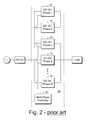
- FIG. 2shows a simplified, exemplary electronic system according to the '566 patent.
- the DC—DC converteris split into multiple phases 1-M (elements 21 to 24 ), which are controlled by a multi-phase controller 26 .
- the phases 1-Mare out of phase with each other.
- Each DC—DC phasecontributes to the overall output current provided to the load.
- the multi-phase controllersequences the phases to reduce ripple at the input and the output.
- the N+1 redundant DC—DC unit 10is there to continue powering the load.
- the loadwill be underpowered, or the remaining DC—DC phases will have to work harder to make up for the lost DC—DC phase(s). This may lead to premature failure of the overall DC—DC system, as the surviving DC—DC phases may have to work beyond their design parameters. In some cases, loss of one or more DC—DC phases may even result in a domino effect that takes down the other DC—DC phases, resulting in a loss of power to the load, or perhaps even destruction of the load.
- the present inventionoffers a more insightful, efficient, and inexpensive solution.
- FIG. 1Aillustrates an electronic system having a redundant DC—DC power supply, according to the prior art.
- FIG. 1Billustrates an electronic system powered by a synchronous multi-phase buck regulator, according to the prior art.
- FIG. 2illustrates an electronic system having a multi-phase DC—DC power supply, according to the prior art.
- FIG. 3illustrates an electronic system having a short-protected multi-phase DC—DC power supply, according to one embodiment of this invention.
- FIG. 4illustrates one embodiment of the short-protected multi-phase DC—DC power supply of this invention.
- FIG. 5illustrates another embodiment of the invention, in which a redundant DC—DC phase is ordinarily decoupled from the load.
- FIG. 3shows a system powered by one embodiment of the short-protected multi-phase DC—DC power supply 30 of this invention.
- the power supplyincludes two or more DC—DC phases, illustrated here as DC—DC phase 1 ( 31 ), DC—DC phase 2 ( 32 ), DC—DC phase 3 ( 33 ), up to DC—DC phase M ( 34 ).
- DC—DC phase 131
- DC—DC phase 232
- DC—DC phase 333
- DC—DC phase M34
- the phasesare powered by an AC-DC converter and are under the control of a multi-phase controller, to power a load.
- Each DC—DC phasereceives its own synchronization signal S 1 through SM, also known as switching signals, from the multi-phase controller.
- DC—DC phase 1illustrates details which may also be present in the other DC—DC phases.
- DC—DC phase 1includes a duty cycle controller 35 , a gate driver 36 , a short detector 37 , a short protector 38 , and a start-up controller or circuit 39 .
- all DC—DC phasesare of identical construction, while in other embodiments, they may differ from each other.
- various of the sub-components shownmay be optional, redundantly provided, and so forth.
- FIG. 4shows one exemplary embodiment of such a DC—DC phase ( 40 ).
- the readerwill appreciate that there are many ways and circuits in which the principles of this invention may be constructed, and that the specific circuitry shown in FIG. 4 is only by way of illustration and not limitation.
- the DC—DC phasereceives its respective synchronization or switching signal (in this example S 1 ) from the multi-phase controller at an input node.
- the synchronization signalis routed through an RC network (R 6 , C 3 , R 4 ) and through a diode D 2 , at which point it is regarded as signal SG 1 , which is to the input node of a top detector shutdown switch Q 1 .
- the switching signal SG 1turns the shutdown switch Q 1 and keeps it on in the normal operating mode, and turns the shutdown switch Q 1 off if top switch Q 2 or the bottom switch Q 3 fail short.
- the top detector shutdown switchis connected to the +V power rail input and to the synchronous multi-phase buck regulator, which includes top switch Q 2 and bottom switch Q 3 .
- the duty cycle control signals SG 2 and SG 3are provided from the duty cycle controller to the gates of the top and bottom switches.
- the duty cycle controllerwould provide a 10% duty cycle, in which SG 2 is held active for 10% and inactive for 90% of the time, while SG 3 is held inactive for 10% and active for 90% of the time.
- the switch node of the buck regulatoris coupled through a feedback loop including a capacitor C 4 to the input of the diode D 2 to provide enough charge or voltage to keep the shutdown switch Q 1 on in normal operating conditions.
- the switch nodeis also coupled through an inductor L 1 and the bottom detector shutdown switch Q 4 to the output node of the DC—DC phase, where it provides Vcc to the load.
- the bottom detector shutdown switchis connected so as to enable its FET body diode to provide the protection against current reversal which was provided in FIG. 1B by diode D 0 .
- the FET Q 4offers very low impedance so it will only produce a tiny fraction of the heat, and consume only a tiny fraction of the power as compared to the prior diode solution (DO of FIG. 1 B).
- the top switch detector shutdown switch Q 1activates by becoming an “open”, isolating the top switch, switch node, and the load from the +V rail. If Q 2 shorts, the gate of Q 1 goes low and discharges, turning off Q 1 , which isolates Q 2 .
- the bottom detector shutdown switch Q 4isolates the load from the buck regulator. Or, more to the point, the bottom detector shutdown switch isolates the failed buck regulator's output from those of the other DC—DC phases (shown in FIG. 3 ), which might shut down the system or otherwise cause their destruction as they would have a direct output path to ground.
- a comparator U 1monitors the voltage across the bottom detector shutdown switch Q 4 , and if Q 3 shorts and causes a back-current to feed from the load into the DC—DC phase, the comparator turns off the bottom detector shutdown switch, isolating this DC—DC phase. In this case, the diode D 1 provides latching to keep the bottom detector shutdown switch off, preventing it from cycling on and off.
- Resistors R 1 and R 9provide hysteresis to help eliminate false triggering of the comparator.
- the switch nodeBecause at start-up the regulator is not yet in full operation, the switch node is not yet switched, so it cannot provide the boost voltage (a square wave) to C 4 , through a diode D 2 to keep Q 1 on.
- the switch nodeAfter the regulator is up and running, the switch node will provide enough boost voltage to sustain and keep Q 1 on through C 4 , D 2 , then Q 5 turns S 1 off by closing and providing a path to ground so the S 1 pulse is fed to ground and isolated from the rest of the circuit shown in FIG. 4, but the S 1 pulse is still fed to the gate driver circuit (not shown in FIG. 4, but shown as 36 in FIG. 3 ).
- the S 1 signalis a positive-going pulse, which goes through the resistor R 6 and coupled through the capacitor C 3 and charges the capacitor C 4 , presenting a voltage higher than +V at the junction of diodes D 2 and D 3 .
- This voltagegoes on through diode D 2 to the gate of Q 1 , turning on Q 1 and providing the pass element Q 2 with the +V voltage.
- the capacitor C 4couples the switching voltage to provide a boost voltage to drive the gate of Q 1 .
- the output voltage Vccrises above 0.6 volts (a junction drop)
- Q 5turns on and disables the startup voltage. If a pass element fault occurs, the pulse occurring at the source of Q 2 will be interrupted and the boost voltage will be drained off by resistor R 7 , turning off Q 1 .
- a pass elementhas a failure, its series element will shut down, and will then shut down the phase pass element. If a synchronous element has a failure, the phase pass element will shut down and the series element will shut down.
- FIG. 5shows another embodiment 50 of the invention, in which one or more of the redundant DC—DC phases are ordinarily decoupled from the load and are kept in reserve, for use in case another DC—DC phase fails.
- FIG. 5shows only a single DC—DC phase M having this mechanism for being held in reserve.
- the power output of the redundant DC—DC phase Mis coupled to the load through a switch 51 , which is activated in response to one or more of the other DC—DC phases.
- “OK” or “running normally” outputs OK 1 -OK 4 of these other DC—DC phasesare active high and control the switch via a NAND gate 52 .
- the SG 1 signals(as illustrated in FIG. 4) of the non-reserve phases may be used as the OK signals.
- drawings showing methods, and the written descriptions thereof,should also be understood to illustrate machine-accessible media having recorded, encoded, or otherwise embodied therein instructions, functions, routines, control codes, firmware, software, or the like, which, when accessed, read, executed, loaded into, or otherwise utilized by a machine, will cause the machine to perform the illustrated methods.
- Such mediamay include, by way of illustration only and not limitation: magnetic, optical, magneto-optical, or other storage mechanisms, fixed or removable discs, drives, tapes, semiconductor memories, organic memories, CD-ROM, CD-R, CD-RW, DVD-ROM, DVD-R, DVD-RW, Zip, floppy, cassette, reel-to-reel, or the like.
- the machinesmay alternatively include down-the-wire, broadcast, or other delivery mechanisms such as Internet, local area network, wide area network, wireless, cellular, cable, laser, satellite, microwave, or other suitable carrier means, over which the instructions etc. may be delivered in the form of packets, serial data, parallel data, or other suitable format.
- the machinemay include, by way of illustration only and not limitation: microprocessor, embedded controller, PLA, PAL, FPGA, ASIC, computer, smart card, networking equipment, or any other machine, apparatus, system, or the like which is adapted to perform functionality defined by such instructions or the like.
- Such drawings, written descriptions, and corresponding claimsmay variously be understood as representing the instructions etc. taken alone, the instructions etc. as organized in their particular packet/serial/parallel/etc.
Landscapes
- Engineering & Computer Science (AREA)
- Power Engineering (AREA)
- Dc-Dc Converters (AREA)
Abstract
Description
1. Technical Field of the Invention
The present invention relates generally to DC—DC converters and voltage regulators, and more specifically to a multi-phase DC—DC converter having redundant DC—DC phases or modules isolated by short protection mechanisms.
2. Background Art
FIG. 1A shows a simplified example of an electronic system5 according to the prior art. The system is powered by anAC source 6, to which is connected an AC-DC converter 7. One component of a DC-powered electronic system which is known to be subject to various types of failures, is the DC—DC converter 8, whose primary function is typically to step the DC voltage down from e.g. 12 volts provided by the AC-DC converter to 5 volts or 3.3 volts or whatever is required by the particular load9 for which the system is designed. Therefore, in previous systems it has been known to provide a redundant or duplicate DC—DC converter 10 in parallel with the primary DC—DC converter 7. This is commonly known as “N+1 redundancy”. Unfortunately, this seldom-used protection has meant doubling the cost of the DC—DC converter portion of the system.
FIG. 1B shows an exemplary DC—DC converter8 (or10), such as may be used in the system of FIG.1A. The DC—DC converter 8 includes aduty cycle controller 11 which provides duty cycle control signals SG2 and SG3 to respective switches Q2 (“top switch”) and Q3 (“bottom switch”) of a synchronousmulti-phase buck regulator 12. The top switch Q2 is often called a pass switching element, and the bottom switch Q3 is often called a synchronous switching element. The output of theregulator 12 is taken from the switch node between the two switches, and is fed to an inductor L1 which stores energy and feeds into a diode DO which prevents current from returning into the regulator from the load. The inductor L1 and capacitor C1 smooth the provided voltage and amperage over time. A capacitor C2 is coupled across the load to assist the regulator by providing current in response to changing demands from the load.
James Dinh is co-inventor of the present invention and is the inventor of a related invention disclosed in U.S. Pat. No. 6,262,566 “DC-to-DC Controller Having a Multi-Phase Synchronous Buck Regulator” which issued Jul. 17, 2001. Both this patent and that one are assigned to Intel Corporation.
FIG. 2 shows a simplified, exemplary electronic system according to the '566 patent. In that system, the DC—DC converter is split into multiple phases 1-M (elements 21 to24), which are controlled by amulti-phase controller 26. In general, the phases 1-M are out of phase with each other. Each DC—DC phase contributes to the overall output current provided to the load. The multi-phase controller sequences the phases to reduce ripple at the input and the output.
In the system of FIG. 1A, if the main DC—DC unit 8 fails, the N+1 redundant DC—DC unit 10 is there to continue powering the load. In the system of FIG. 2, if any of the DC—DC phases fails, either the load will be underpowered, or the remaining DC—DC phases will have to work harder to make up for the lost DC—DC phase(s). This may lead to premature failure of the overall DC—DC system, as the surviving DC—DC phases may have to work beyond their design parameters. In some cases, loss of one or more DC—DC phases may even result in a domino effect that takes down the other DC—DC phases, resulting in a loss of power to the load, or perhaps even destruction of the load.
If one were willing to bear the cost of doubling-up the DC—DC componentry, one could impose the FIG. 1A N+1 thinking on the FIG. 2 system, and have two complete sets of DC—DC converter 20 in an N+1 redundant system.
The present invention, however, offers a more insightful, efficient, and inexpensive solution.
The invention will be understood more fully from the detailed description given below and from the accompanying drawings of embodiments of the invention which, however, should not be taken to limit the invention to the specific embodiments described, but are for explanation and understanding only.
FIG. 1A illustrates an electronic system having a redundant DC—DC power supply, according to the prior art.
FIG. 1B illustrates an electronic system powered by a synchronous multi-phase buck regulator, according to the prior art.
FIG. 2 illustrates an electronic system having a multi-phase DC—DC power supply, according to the prior art.
FIG. 3 illustrates an electronic system having a short-protected multi-phase DC—DC power supply, according to one embodiment of this invention.
FIG. 4 illustrates one embodiment of the short-protected multi-phase DC—DC power supply of this invention.
FIG. 5 illustrates another embodiment of the invention, in which a redundant DC—DC phase is ordinarily decoupled from the load.
FIG. 3 shows a system powered by one embodiment of the short-protected multi-phase DC—DC power supply 30 of this invention. The power supply includes two or more DC—DC phases, illustrated here as DC—DC phase1 (31), DC—DC phase2 (32), DC—DC phase3 (33), up to DC—DC phase M (34). The reader will appreciate that any suitable number of phases may be employed. As in the prior art, the phases are powered by an AC-DC converter and are under the control of a multi-phase controller, to power a load. Each DC—DC phase receives its own synchronization signal S1 through SM, also known as switching signals, from the multi-phase controller.
DC—DC phase 1 illustrates details which may also be present in the other DC—DC phases. DC—DC phase 1 includes aduty cycle controller 35, agate driver 36, ashort detector 37, ashort protector 38, and a start-up controller orcircuit 39. In some embodiments, all DC—DC phases are of identical construction, while in other embodiments, they may differ from each other. In some embodiments, various of the sub-components shown may be optional, redundantly provided, and so forth.
FIG. 4 shows one exemplary embodiment of such a DC—DC phase (40). The reader will appreciate that there are many ways and circuits in which the principles of this invention may be constructed, and that the specific circuitry shown in FIG. 4 is only by way of illustration and not limitation.
The DC—DC phase receives its respective synchronization or switching signal (in this example S1) from the multi-phase controller at an input node. The synchronization signal is routed through an RC network (R6, C3, R4) and through a diode D2, at which point it is regarded as signal SG1, which is to the input node of a top detector shutdown switch Q1. The switching signal SG1 turns the shutdown switch Q1 and keeps it on in the normal operating mode, and turns the shutdown switch Q1 off if top switch Q2 or the bottom switch Q3 fail short. The top detector shutdown switch is connected to the +V power rail input and to the synchronous multi-phase buck regulator, which includes top switch Q2 and bottom switch Q3. As in the prior art, the duty cycle control signals SG2 and SG3 are provided from the duty cycle controller to the gates of the top and bottom switches.
In a system in which the +V output of the AC-DC converter is 12 volts, and the desired Vcc voltage output to the load is 1.2 volts, the duty cycle controller would provide a 10% duty cycle, in which SG2 is held active for 10% and inactive for 90% of the time, while SG3 is held inactive for 10% and active for 90% of the time.
The switch node of the buck regulator is coupled through a feedback loop including a capacitor C4 to the input of the diode D2 to provide enough charge or voltage to keep the shutdown switch Q1 on in normal operating conditions.
The switch node is also coupled through an inductor L1 and the bottom detector shutdown switch Q4 to the output node of the DC—DC phase, where it provides Vcc to the load. The bottom detector shutdown switch is connected so as to enable its FET body diode to provide the protection against current reversal which was provided in FIG. 1B by diode D0. However, because the body diode will be shorted out by the FET Q4 when the FET Q4 is on in normal operating conditions, the FET Q4 offers very low impedance so it will only produce a tiny fraction of the heat, and consume only a tiny fraction of the power as compared to the prior diode solution (DO of FIG.1B).
In operation, if the buck regulator's top switch Q2 suffers a failure in which it shorts out and becomes, in essence, a wire connecting the switch node to the +V rail (which would, in a prior art system, likely destroy the load by coupling it to +V rather than the much lower Vcc), the top switch detector shutdown switch Q1 activates by becoming an “open”, isolating the top switch, switch node, and the load from the +V rail. If Q2 shorts, the gate of Q1 goes low and discharges, turning off Q1, which isolates Q2.
Similarly, if the buck regulator's bottom switch Q3 suffers a shorting failure, the bottom detector shutdown switch Q4 isolates the load from the buck regulator. Or, more to the point, the bottom detector shutdown switch isolates the failed buck regulator's output from those of the other DC—DC phases (shown in FIG.3), which might shut down the system or otherwise cause their destruction as they would have a direct output path to ground. A comparator U1 monitors the voltage across the bottom detector shutdown switch Q4, and if Q3 shorts and causes a back-current to feed from the load into the DC—DC phase, the comparator turns off the bottom detector shutdown switch, isolating this DC—DC phase. In this case, the diode D1 provides latching to keep the bottom detector shutdown switch off, preventing it from cycling on and off. Resistors R1 and R9 provide hysteresis to help eliminate false triggering of the comparator.
Because at start-up the regulator is not yet in full operation, the switch node is not yet switched, so it cannot provide the boost voltage (a square wave) to C4, through a diode D2 to keep Q1 on. After the regulator is up and running, the switch node will provide enough boost voltage to sustain and keep Q1 on through C4, D2, then Q5 turns S1 off by closing and providing a path to ground so the S1 pulse is fed to ground and isolated from the rest of the circuit shown in FIG. 4, but the S1 pulse is still fed to the gate driver circuit (not shown in FIG. 4, but shown as36 in FIG.3).
At startup, the S1 signal is a positive-going pulse, which goes through the resistor R6 and coupled through the capacitor C3 and charges the capacitor C4, presenting a voltage higher than +V at the junction of diodes D2 and D3. This voltage goes on through diode D2 to the gate of Q1, turning on Q1 and providing the pass element Q2 with the +V voltage. As the converter begins to run normally, the capacitor C4 couples the switching voltage to provide a boost voltage to drive the gate of Q1. When the output voltage Vcc rises above 0.6 volts (a junction drop), Q5 turns on and disables the startup voltage. If a pass element fault occurs, the pulse occurring at the source of Q2 will be interrupted and the boost voltage will be drained off by resistor R7, turning off Q1.
If a pass element has a failure, its series element will shut down, and will then shut down the phase pass element. If a synchronous element has a failure, the phase pass element will shut down and the series element will shut down.
FIG. 5 shows anotherembodiment 50 of the invention, in which one or more of the redundant DC—DC phases are ordinarily decoupled from the load and are kept in reserve, for use in case another DC—DC phase fails. For simplicity of illustration, FIG. 5 shows only a single DC—DC phase M having this mechanism for being held in reserve. In one embodiment, the power output of the redundant DC—DC phase M is coupled to the load through aswitch 51, which is activated in response to one or more of the other DC—DC phases. In one such embodiment, “OK” or “running normally” outputs OK1-OK4 of these other DC—DC phases are active high and control the switch via aNAND gate 52. In this mode, if any of the DC—DC phases suffers a failure, its OK signal will drop to ground, and the output of the NAND gate will go high, turning on the switch. In one such embodiment, the SG1 signals (as illustrated in FIG. 4) of the non-reserve phases may be used as the OK signals.
The reader will appreciate that this is only one simplistic method of holding one or more of the DC—DC phases in reserve. This method enables the reserve DC—DC phases to be up and running prior to their being called into action, yet prevents them from consuming significant power, which limits wear and tear on their devices. In other embodiments, it may be desirable to keep the reserve units completely inactive until they are needed, to further reduce power consumption.
The reader should appreciate that drawings showing methods, and the written descriptions thereof, should also be understood to illustrate machine-accessible media having recorded, encoded, or otherwise embodied therein instructions, functions, routines, control codes, firmware, software, or the like, which, when accessed, read, executed, loaded into, or otherwise utilized by a machine, will cause the machine to perform the illustrated methods. Such media may include, by way of illustration only and not limitation: magnetic, optical, magneto-optical, or other storage mechanisms, fixed or removable discs, drives, tapes, semiconductor memories, organic memories, CD-ROM, CD-R, CD-RW, DVD-ROM, DVD-R, DVD-RW, Zip, floppy, cassette, reel-to-reel, or the like. They may alternatively include down-the-wire, broadcast, or other delivery mechanisms such as Internet, local area network, wide area network, wireless, cellular, cable, laser, satellite, microwave, or other suitable carrier means, over which the instructions etc. may be delivered in the form of packets, serial data, parallel data, or other suitable format. The machine may include, by way of illustration only and not limitation: microprocessor, embedded controller, PLA, PAL, FPGA, ASIC, computer, smart card, networking equipment, or any other machine, apparatus, system, or the like which is adapted to perform functionality defined by such instructions or the like. Such drawings, written descriptions, and corresponding claims may variously be understood as representing the instructions etc. taken alone, the instructions etc. as organized in their particular packet/serial/parallel/etc. form, and/or the instructions etc. together with their storage or carrier media. The reader will further appreciate that such instructions etc. may be recorded or carried in compressed, encrypted, or rag otherwise encoded format without departing from the scope of this patent, even if the instructions etc. must be decrypted, decompressed, compiled, interpreted, or otherwise manipulated prior to their execution or other utilization by the machine.
Reference in the specification to “an embodiment,” “one embodiment,” “some embodiments,” or “other embodiments” means that a particular feature, structure, or characteristic described in connection with the embodiments is included in at least some embodiments, but not necessarily all embodiments, of the invention. The various appearances “an embodiment,” “one embodiment,” or “some embodiments” are not necessarily all referring to the same embodiments.
If the specification states a component, feature, structure, or characteristic “may”, “might”, or “could” be included, that particular component, feature, structure, or characteristic is not required to be included. If the specification or claim refers to “a” or “an” element, that does not mean there is only one of the element. If the specification or claims refer to “an additional” element, that does not preclude there being more than one of the additional element.
Those skilled in the art having the benefit of this disclosure will appreciate that many other variations from the foregoing description and drawings may be made within the scope of the present invention. Indeed, the invention is not limited to the details described above. Rather, it is the following claims including any amendments thereto that define the scope of the invention.
Claims (24)
1. A DC—DC regulator comprising:
a plurality of DC—DC phases, at least one of which includes,
a regulator, and
a detector shutdown switch coupled to isolate the regulator in response to the regulator having a short-circuit failure;
a redundant DC phase; and
a circuit to connect the redundant DC phase in response to the short-circuit failure in the at least one of the DC phases.
2. The DC—DC regulator ofclaim 1 wherein the detector shutdown switch comprises:
a top detector shutdown switch.
3. The DC—DC regulator ofclaim 1 wherein the detector shutdown switch comprises:
a bottom detector shutdown switch.
4. The DC—DC regulator ofclaim 1 wherein the detector shutdown switch comprises:
a top detector shutdown switch; and
a bottom detector shutdown switch.
5. The DC—DC regulator ofclaim 1 wherein the detector shutdown switch is coupled to isolate the regulator from a load.
6. The DC—DC regulator ofclaim 1 wherein the detector shutdown switch is coupled to isolate the regulator from a regulator of another of the DC—DC phases.
7. The DC—DC regulator ofclaim 1 wherein the detector shutdown switch comprises:
a field-effect transistor (FET) having a FET body diode coupled to inhibit current flow from a load back into the DC—DC regulator.
8. The DC—DC regulator ofclaim 1 wherein the regulator comprises:
a synchronous multi-phase buck regulator; and
a duty cycle controller coupled to provide duty cycle signals to the synchronous multi-phase buck regulator.
9. The DC—DC regulator ofclaim 1 further comprising:
a multi-phase controller coupled to provide respective switching signals to the plurality of DC—DC phases.
10. The DC—DC regulator ofclaim 9 further comprising:
a startup controller.
11. A synchronous multi-phase buck regulator to provide DC voltage to a load and comprising:
a top switch;
a switching node;
a bottom switch coupled to the top switch at the switching node;
an output node to be coupled to the load;
a first shutdown switch coupled in series between the switching node and the output node, the first shutdown switch comprising a field-effect transistor (FET) having a FET body diode coupled to inhibit current flow from the output node to the switch node; and
a comparator having inputs coupled across the FET and an output coupled to a gate of the FET.
12. The synchronous multi-phase buck regulator ofclaim 11 further comprising:
a resistor coupled in series between the FET and an input of the comparator.
13. The synchronous multi-phase buck regulator ofclaim 12 further comprising:
another resistor coupled in series between the FET and another input of the comparator.
14. The synchronous multi-phase buck regulator ofclaim 12 further comprising:
a diode coupled between an input of the comparator and the gate of the FET.
15. The synchronous multi-phase buck regulator ofclaim 11 to generate the DC voltage from another DC voltage, and further comprising:
an input node to receive the other DC voltage; and
a second shutdown switch coupled between the input node and the top switch.
16. The synchronous multi-phase buck regulator ofclaim 11 further comprising:
a phase control input to receive a switching signal; and
a third switch coupled to the output node and the phase control input node to inhibit the switching signal in response to the synchronous multi-phase buck regulator achieving a normal state of operation.
17. An electronic system comprising:
a load having an input; and
a DC—DC converter including,
a duty cycle controller, and
a plurality of DC—DC phases, each including,
a buck regulator having an input coupled to the duty cycle controller and having a switch node coupled to the input of the load,
a top shutdown switch coupled to the buck regulator, and
a bottom shutdown switch coupled to the buck regulator;
the plurality of DC—DC phases comprising a plurality of normal operation DC—DC phases; and
at least one reserve DC—DC phase.
18. The electronic system ofclaim 17 further comprising:
an AC-DC converter coupled to the DC—DC converter.
19. The electronic system ofclaim 18 wherein:
the bottom shutdown switch comprises a field effect transistor (FET) having a FET body diode coupled to inhibit current flow from the load to the buck regulator.
20. An article of manufacture comprising:
a machine-accessible medium having thereon data which, when accessed by a machine, enable the machine to create a semiconductor device including,
a multi-phase DC—DC converter including,
a synchronous multi-phase buck regulator, and
a shutdown switch coupled to the buck regulator to defeat the buck regulator in response to the buck regulator suffering a short circuit.
21. The article of manufacture ofclaim 20 wherein the machine-accessible medium has additional data that, when accessed by the machine, enable the machine to include in the multi-phase DC—DC converter:
a field-effect transistor (FET) having a FET body diode coupled to inhibit current flow from a load back into an output of the buck regulator.
22. The article of manufacture ofclaim 21 wherein the machine-accessible medium has additional data that, when accessed by the machine, enable the machine to include in the multi-phase DC—DC converter:
a reserve DC—DC phase in the multi-phase DC—DC converter.
23. The article of manufacture ofclaim 21 wherein the machine-accessible medium comprises a recording medium.
24. The article of manufacture ofclaim 21 wherein the machine-accessible medium comprises a communication link and the data comprise a carrier wave traversing the communication link.
Priority Applications (1)
| Application Number | Priority Date | Filing Date | Title |
|---|---|---|---|
| US10/000,737US6650556B2 (en) | 2001-10-31 | 2001-10-31 | Multi-phase DC—DC converter |
Applications Claiming Priority (1)
| Application Number | Priority Date | Filing Date | Title |
|---|---|---|---|
| US10/000,737US6650556B2 (en) | 2001-10-31 | 2001-10-31 | Multi-phase DC—DC converter |
Publications (2)
| Publication Number | Publication Date |
|---|---|
| US20030081438A1 US20030081438A1 (en) | 2003-05-01 |
| US6650556B2true US6650556B2 (en) | 2003-11-18 |
Family
ID=21692798
Family Applications (1)
| Application Number | Title | Priority Date | Filing Date |
|---|---|---|---|
| US10/000,737Expired - Fee RelatedUS6650556B2 (en) | 2001-10-31 | 2001-10-31 | Multi-phase DC—DC converter |
Country Status (1)
| Country | Link |
|---|---|
| US (1) | US6650556B2 (en) |
Cited By (83)
| Publication number | Priority date | Publication date | Assignee | Title |
|---|---|---|---|---|
| US20030030328A1 (en)* | 2001-08-07 | 2003-02-13 | Yazaki Corporation | Power distribution apparatus and intermediate connector therein |
| US20030142513A1 (en)* | 2002-01-31 | 2003-07-31 | Patrizio Vinciarelli | Factorized power architecture with point of load sine amplitude converters |
| US20030197245A1 (en)* | 2002-04-03 | 2003-10-23 | International Rectifier Corporation | Multiphase synchronous buck converter with improved output current sharing |
| US20030227280A1 (en)* | 2002-01-31 | 2003-12-11 | Patrizio Vinciarelli | Factorized power architecture with point of load sine amplitude converters |
| US20040120169A1 (en)* | 2002-12-20 | 2004-06-24 | Gerhard Schrom | Hysteretic DC-DC converters |
| US20050006956A1 (en)* | 2003-07-09 | 2005-01-13 | Fong Shi | Redundant power distribution system |
| US20050286191A1 (en)* | 2004-06-28 | 2005-12-29 | Pieter Vorenkamp | Power supply integrated circuit with multiple independent outputs |
| US20060071649A1 (en)* | 2004-09-30 | 2006-04-06 | Gerhard Schrom | Apparatus and method for multi-phase transformers |
| US20070013358A1 (en)* | 2005-06-30 | 2007-01-18 | Gerhard Schrom | Multiphase transformer for a multiphase DC-DC converter |
| US20070097571A1 (en)* | 2005-07-07 | 2007-05-03 | Intel Corporation | Multiphase voltage regulation using paralleled inductive circuits having magnetically coupled inductors |
| US20090066307A1 (en)* | 2007-09-10 | 2009-03-12 | Analog Devices, Inc. | Efficient voltage converter methods and structures |
| US20100033019A1 (en)* | 2008-08-06 | 2010-02-11 | Noribachi Llc | Modular solar device power distribution |
| TWI492018B (en)* | 2013-12-16 | 2015-07-11 | ||
| US9654007B1 (en) | 2016-06-22 | 2017-05-16 | Dialog Semiconductor (Uk) Limited | Regulation of a multiple stage switch mode power converter through an intermediate voltage control |
| US9800131B1 (en)* | 2016-05-11 | 2017-10-24 | Anpec Electronics Corporation | Phase controller and multi-phase voltage converter using the same |
| US9859707B2 (en) | 2014-09-11 | 2018-01-02 | Cpg Technologies, Llc | Simultaneous multifrequency receive circuits |
| US9857402B2 (en) | 2015-09-08 | 2018-01-02 | CPG Technologies, L.L.C. | Measuring and reporting power received from guided surface waves |
| US9882397B2 (en) | 2014-09-11 | 2018-01-30 | Cpg Technologies, Llc | Guided surface wave transmission of multiple frequencies in a lossy media |
| US9882436B2 (en) | 2015-09-09 | 2018-01-30 | Cpg Technologies, Llc | Return coupled wireless power transmission |
| US9882606B2 (en) | 2015-09-09 | 2018-01-30 | Cpg Technologies, Llc | Hybrid guided surface wave communication |
| US9887558B2 (en) | 2015-09-09 | 2018-02-06 | Cpg Technologies, Llc | Wired and wireless power distribution coexistence |
| US9887556B2 (en) | 2014-09-11 | 2018-02-06 | Cpg Technologies, Llc | Chemically enhanced isolated capacitance |
| US9887587B2 (en) | 2014-09-11 | 2018-02-06 | Cpg Technologies, Llc | Variable frequency receivers for guided surface wave transmissions |
| US9885742B2 (en) | 2015-09-09 | 2018-02-06 | Cpg Technologies, Llc | Detecting unauthorized consumption of electrical energy |
| US9887585B2 (en) | 2015-09-08 | 2018-02-06 | Cpg Technologies, Llc | Changing guided surface wave transmissions to follow load conditions |
| US9887557B2 (en) | 2014-09-11 | 2018-02-06 | Cpg Technologies, Llc | Hierarchical power distribution |
| US9893402B2 (en) | 2014-09-11 | 2018-02-13 | Cpg Technologies, Llc | Superposition of guided surface waves on lossy media |
| US9893403B2 (en) | 2015-09-11 | 2018-02-13 | Cpg Technologies, Llc | Enhanced guided surface waveguide probe |
| US9899718B2 (en) | 2015-09-11 | 2018-02-20 | Cpg Technologies, Llc | Global electrical power multiplication |
| US9912031B2 (en)* | 2013-03-07 | 2018-03-06 | Cpg Technologies, Llc | Excitation and use of guided surface wave modes on lossy media |
| US9910144B2 (en) | 2013-03-07 | 2018-03-06 | Cpg Technologies, Llc | Excitation and use of guided surface wave modes on lossy media |
| US9921256B2 (en) | 2015-09-08 | 2018-03-20 | Cpg Technologies, Llc | Field strength monitoring for optimal performance |
| US9923385B2 (en) | 2015-06-02 | 2018-03-20 | Cpg Technologies, Llc | Excitation and use of guided surface waves |
| US9941566B2 (en) | 2014-09-10 | 2018-04-10 | Cpg Technologies, Llc | Excitation and use of guided surface wave modes on lossy media |
| US9960470B2 (en) | 2014-09-11 | 2018-05-01 | Cpg Technologies, Llc | Site preparation for guided surface wave transmission in a lossy media |
| US9997040B2 (en) | 2015-09-08 | 2018-06-12 | Cpg Technologies, Llc | Global emergency and disaster transmission |
| US10001553B2 (en) | 2014-09-11 | 2018-06-19 | Cpg Technologies, Llc | Geolocation with guided surface waves |
| US10027177B2 (en) | 2015-09-09 | 2018-07-17 | Cpg Technologies, Llc | Load shedding in a guided surface wave power delivery system |
| US10027116B2 (en) | 2014-09-11 | 2018-07-17 | Cpg Technologies, Llc | Adaptation of polyphase waveguide probes |
| US10027131B2 (en) | 2015-09-09 | 2018-07-17 | CPG Technologies, Inc. | Classification of transmission |
| US10033198B2 (en) | 2014-09-11 | 2018-07-24 | Cpg Technologies, Llc | Frequency division multiplexing for wireless power providers |
| US10062944B2 (en) | 2015-09-09 | 2018-08-28 | CPG Technologies, Inc. | Guided surface waveguide probes |
| US10063095B2 (en) | 2015-09-09 | 2018-08-28 | CPG Technologies, Inc. | Deterring theft in wireless power systems |
| US10064254B1 (en) | 2017-06-01 | 2018-08-28 | Cooper Technologies Company | Multi-phase power supplies for light fixtures |
| US10074993B2 (en) | 2014-09-11 | 2018-09-11 | Cpg Technologies, Llc | Simultaneous transmission and reception of guided surface waves |
| US10079573B2 (en) | 2014-09-11 | 2018-09-18 | Cpg Technologies, Llc | Embedding data on a power signal |
| US10084223B2 (en) | 2014-09-11 | 2018-09-25 | Cpg Technologies, Llc | Modulated guided surface waves |
| US10101444B2 (en) | 2014-09-11 | 2018-10-16 | Cpg Technologies, Llc | Remote surface sensing using guided surface wave modes on lossy media |
| US10103452B2 (en) | 2015-09-10 | 2018-10-16 | Cpg Technologies, Llc | Hybrid phased array transmission |
| US10122218B2 (en) | 2015-09-08 | 2018-11-06 | Cpg Technologies, Llc | Long distance transmission of offshore power |
| US10135301B2 (en) | 2015-09-09 | 2018-11-20 | Cpg Technologies, Llc | Guided surface waveguide probes |
| US10141622B2 (en) | 2015-09-10 | 2018-11-27 | Cpg Technologies, Llc | Mobile guided surface waveguide probes and receivers |
| WO2018222196A1 (en)* | 2017-06-01 | 2018-12-06 | Cooper Technologies Company | Multi-phase power supplies for light fixtures |
| US10175048B2 (en) | 2015-09-10 | 2019-01-08 | Cpg Technologies, Llc | Geolocation using guided surface waves |
| US10175203B2 (en) | 2014-09-11 | 2019-01-08 | Cpg Technologies, Llc | Subsurface sensing using guided surface wave modes on lossy media |
| US10193595B2 (en) | 2015-06-02 | 2019-01-29 | Cpg Technologies, Llc | Excitation and use of guided surface waves |
| US10193229B2 (en) | 2015-09-10 | 2019-01-29 | Cpg Technologies, Llc | Magnetic coils having cores with high magnetic permeability |
| US10205326B2 (en) | 2015-09-09 | 2019-02-12 | Cpg Technologies, Llc | Adaptation of energy consumption node for guided surface wave reception |
| US10230270B2 (en) | 2015-09-09 | 2019-03-12 | Cpg Technologies, Llc | Power internal medical devices with guided surface waves |
| US10312747B2 (en) | 2015-09-10 | 2019-06-04 | Cpg Technologies, Llc | Authentication to enable/disable guided surface wave receive equipment |
| US10324163B2 (en) | 2015-09-10 | 2019-06-18 | Cpg Technologies, Llc | Geolocation using guided surface waves |
| US10396566B2 (en) | 2015-09-10 | 2019-08-27 | Cpg Technologies, Llc | Geolocation using guided surface waves |
| US10408915B2 (en) | 2015-09-10 | 2019-09-10 | Cpg Technologies, Llc | Geolocation using guided surface waves |
| US10408916B2 (en) | 2015-09-10 | 2019-09-10 | Cpg Technologies, Llc | Geolocation using guided surface waves |
| US10447342B1 (en) | 2017-03-07 | 2019-10-15 | Cpg Technologies, Llc | Arrangements for coupling the primary coil to the secondary coil |
| US10498393B2 (en) | 2014-09-11 | 2019-12-03 | Cpg Technologies, Llc | Guided surface wave powered sensing devices |
| US10498006B2 (en) | 2015-09-10 | 2019-12-03 | Cpg Technologies, Llc | Guided surface wave transmissions that illuminate defined regions |
| US10530257B1 (en) | 2019-03-26 | 2020-01-07 | International Business Machines Corporation | Adding a voltage level to a phase-redundant regulator level |
| US10559867B2 (en) | 2017-03-07 | 2020-02-11 | Cpg Technologies, Llc | Minimizing atmospheric discharge within a guided surface waveguide probe |
| US10559893B1 (en) | 2015-09-10 | 2020-02-11 | Cpg Technologies, Llc | Pulse protection circuits to deter theft |
| US10559866B2 (en) | 2017-03-07 | 2020-02-11 | Cpg Technologies, Inc | Measuring operational parameters at the guided surface waveguide probe |
| US10560147B1 (en) | 2017-03-07 | 2020-02-11 | Cpg Technologies, Llc | Guided surface waveguide probe control system |
| US10566903B1 (en) | 2019-03-26 | 2020-02-18 | International Business Machines Corporation | Sharing redundant regulator phases within a phase-redundant voltage regulator apparatus |
| US10581492B1 (en) | 2017-03-07 | 2020-03-03 | Cpg Technologies, Llc | Heat management around a phase delay coil in a probe |
| US10594217B2 (en) | 2016-09-28 | 2020-03-17 | Dialog Semiconductor (Uk) Limited | Asymmetric two-stage DC-DC switching converter |
| US10606295B1 (en) | 2019-03-26 | 2020-03-31 | International Business Machines Corporation | Sharing redundant regulator phases within a phase-redundant voltage regulator apparatus |
| US10615691B1 (en) | 2019-03-26 | 2020-04-07 | International Business Machines Corporation | Reallocation of regulator phases within a phase-redundant voltage regulator apparatus |
| US10630111B2 (en) | 2017-03-07 | 2020-04-21 | Cpg Technologies, Llc | Adjustment of guided surface waveguide probe operation |
| US10739803B1 (en) | 2019-03-26 | 2020-08-11 | International Business Machines Corporation | Reallocation of regulator phases within a phase-redundant voltage regulator apparatus |
| US10998993B2 (en) | 2015-09-10 | 2021-05-04 | CPG Technologies, Inc. | Global time synchronization using a guided surface wave |
| US20210194371A1 (en)* | 2019-04-08 | 2021-06-24 | Intel Corporation | Discontinuous conduction mode (dcm) voltage regulator circuit with reduced output voltage ripple |
| US11329564B2 (en) | 2019-06-14 | 2022-05-10 | Samsung Sdi Co., Ltd. | Control system for a battery system |
| RU2779907C1 (en)* | 2021-12-09 | 2022-09-15 | Федеральное государственное бюджетное учреждение "16 Центральный научно-исследовательский испытательный ордена Красной Звезды институт имени маршала войск связи А.И. Белова" Министерства обороны Российской Федерации | Three-phase rectifying device |
Families Citing this family (10)
| Publication number | Priority date | Publication date | Assignee | Title |
|---|---|---|---|---|
| US8391036B2 (en)* | 2009-12-29 | 2013-03-05 | International Business Machines Corporation | Selective enablement of power supply sections for improving efficiency |
| JP5924319B2 (en)* | 2013-08-23 | 2016-05-25 | オンキヨー&パイオニアテクノロジー株式会社 | Switching power supply circuit |
| KR101717761B1 (en)* | 2015-06-18 | 2017-03-22 | (주)티에이치엔 | Dual power supply system for vehicle |
| TWI657651B (en)* | 2018-05-23 | 2019-04-21 | 茂達電子股份有限公司 | Frequency compensation circuit used in dc voltage converter |
| WO2020194120A1 (en)* | 2019-03-26 | 2020-10-01 | International Business Machines Corporation | Reallocation of regulator phases within a phase-redundant voltage regulator apparatus |
| CN113632358A (en)* | 2019-03-26 | 2021-11-09 | 国际商业机器公司 | Share redundant regulator phases within a phase redundant voltage regulator device |
| DE102019213076A1 (en)* | 2019-08-30 | 2021-03-04 | Robert Bosch Gmbh | Control device for a DC voltage converter, DC voltage converter and method for controlling a DC voltage converter |
| US11682896B2 (en)* | 2021-06-08 | 2023-06-20 | International Business Machines Corporation | Fault detection in redundant power supplies |
| DE102022207368B4 (en)* | 2022-07-19 | 2024-12-05 | Lenze Se | Method for automatic stability detection of a controller cascade |
| CN115986688B (en)* | 2022-11-25 | 2025-06-27 | 锦浪科技股份有限公司 | Fault isolation method for three-level DC/DC parallel system |
Citations (10)
| Publication number | Priority date | Publication date | Assignee | Title |
|---|---|---|---|---|
| US5270589A (en)* | 1991-01-17 | 1993-12-14 | Kabushiki Kaisha Toshiba | Input/output buffer circuit for semiconductor integrated circuit |
| US5592072A (en)* | 1995-01-24 | 1997-01-07 | Dell Usa, L.P. | High performance dual section voltage regulator |
| US5870296A (en)* | 1997-10-14 | 1999-02-09 | Maxim Integrated Products, Inc. | Dual interleaved DC to DC switching circuits realized in an integrated circuit |
| US5892389A (en)* | 1997-06-03 | 1999-04-06 | Motorola, Inc. | Method and circuit for current limiting of DC-DC regulators |
| US6031743A (en)* | 1998-10-28 | 2000-02-29 | International Business Machines Corporation | Fault isolation in a redundant power converter |
| US6031702A (en)* | 1997-10-22 | 2000-02-29 | Siliconix Incorporated | Short circuit protected DC-DC converter using disconnect switching and method of protecting load against short circuits |
| US6035261A (en)* | 1998-10-28 | 2000-03-07 | International Business Machines Corporation | Fault reporting in a redundant power converter |
| US6055167A (en)* | 1998-08-10 | 2000-04-25 | Custom Power Systems, Inc. | Pulse width modulated boost converter integrated with power factor correction circuit |
| US6362608B1 (en)* | 2001-02-01 | 2002-03-26 | Maxim Integrated Products, Inc. | Multi-phase switching converters and methods |
| US6404175B1 (en)* | 1999-11-15 | 2002-06-11 | Semtech Corporation | Multi-phase and multi-module power supplies with balanced current between phases and modules |
- 2001
- 2001-10-31USUS10/000,737patent/US6650556B2/ennot_activeExpired - Fee Related
Patent Citations (10)
| Publication number | Priority date | Publication date | Assignee | Title |
|---|---|---|---|---|
| US5270589A (en)* | 1991-01-17 | 1993-12-14 | Kabushiki Kaisha Toshiba | Input/output buffer circuit for semiconductor integrated circuit |
| US5592072A (en)* | 1995-01-24 | 1997-01-07 | Dell Usa, L.P. | High performance dual section voltage regulator |
| US5892389A (en)* | 1997-06-03 | 1999-04-06 | Motorola, Inc. | Method and circuit for current limiting of DC-DC regulators |
| US5870296A (en)* | 1997-10-14 | 1999-02-09 | Maxim Integrated Products, Inc. | Dual interleaved DC to DC switching circuits realized in an integrated circuit |
| US6031702A (en)* | 1997-10-22 | 2000-02-29 | Siliconix Incorporated | Short circuit protected DC-DC converter using disconnect switching and method of protecting load against short circuits |
| US6055167A (en)* | 1998-08-10 | 2000-04-25 | Custom Power Systems, Inc. | Pulse width modulated boost converter integrated with power factor correction circuit |
| US6031743A (en)* | 1998-10-28 | 2000-02-29 | International Business Machines Corporation | Fault isolation in a redundant power converter |
| US6035261A (en)* | 1998-10-28 | 2000-03-07 | International Business Machines Corporation | Fault reporting in a redundant power converter |
| US6404175B1 (en)* | 1999-11-15 | 2002-06-11 | Semtech Corporation | Multi-phase and multi-module power supplies with balanced current between phases and modules |
| US6362608B1 (en)* | 2001-02-01 | 2002-03-26 | Maxim Integrated Products, Inc. | Multi-phase switching converters and methods |
Cited By (127)
| Publication number | Priority date | Publication date | Assignee | Title |
|---|---|---|---|---|
| US20030030328A1 (en)* | 2001-08-07 | 2003-02-13 | Yazaki Corporation | Power distribution apparatus and intermediate connector therein |
| US20040183513A1 (en)* | 2002-01-31 | 2004-09-23 | Vlt Corporation, A Texas Corporation | Low-loss transformer-coupled gate driver |
| US20050286271A1 (en)* | 2002-01-31 | 2005-12-29 | Vlt Corporation, A California Corporation | Point of load sine amplitude converters and methods |
| US20030227280A1 (en)* | 2002-01-31 | 2003-12-11 | Patrizio Vinciarelli | Factorized power architecture with point of load sine amplitude converters |
| US6984965B2 (en)* | 2002-01-31 | 2006-01-10 | Vlt, Inc. | Factorized power architecture with point of load sine amplitude converters |
| US20040174147A1 (en)* | 2002-01-31 | 2004-09-09 | Vlt Corporation, A Texas Corporation | Factorized power architecture with point of load sine amplitude converters |
| US20030142513A1 (en)* | 2002-01-31 | 2003-07-31 | Patrizio Vinciarelli | Factorized power architecture with point of load sine amplitude converters |
| US20040184289A1 (en)* | 2002-01-31 | 2004-09-23 | Vlt Corporation, A Texas Corporation | Output resistance modulation in power converters |
| US6975098B2 (en) | 2002-01-31 | 2005-12-13 | Vlt, Inc. | Factorized power architecture with point of load sine amplitude converters |
| US6934166B2 (en) | 2002-01-31 | 2005-08-23 | Vlt, Inc. | Output resistance modulation in power converters |
| US7145786B2 (en)* | 2002-01-31 | 2006-12-05 | Vlt, Inc. | Point of load sine amplitude converters and methods |
| US6911848B2 (en) | 2002-01-31 | 2005-06-28 | Vlt, Inc. | Low-loss transformer-coupled gate driver |
| US6930893B2 (en) | 2002-01-31 | 2005-08-16 | Vlt, Inc. | Factorized power architecture with point of load sine amplitude converters |
| US6803750B2 (en)* | 2002-04-03 | 2004-10-12 | International Rectifier Corporation | Multiphase synchronous buck converter with improved output current sharing |
| US20030197245A1 (en)* | 2002-04-03 | 2003-10-23 | International Rectifier Corporation | Multiphase synchronous buck converter with improved output current sharing |
| US20040120169A1 (en)* | 2002-12-20 | 2004-06-24 | Gerhard Schrom | Hysteretic DC-DC converters |
| US6801026B2 (en)* | 2002-12-20 | 2004-10-05 | Intel Corporation | Hysteretic DC-DC converters |
| US20050006956A1 (en)* | 2003-07-09 | 2005-01-13 | Fong Shi | Redundant power distribution system |
| US7190090B2 (en)* | 2003-07-09 | 2007-03-13 | The Boeing Company | Redundant power distribution system |
| US20050286191A1 (en)* | 2004-06-28 | 2005-12-29 | Pieter Vorenkamp | Power supply integrated circuit with multiple independent outputs |
| US20060071649A1 (en)* | 2004-09-30 | 2006-04-06 | Gerhard Schrom | Apparatus and method for multi-phase transformers |
| US7315463B2 (en) | 2004-09-30 | 2008-01-01 | Intel Corporation | Apparatus and method for multi-phase transformers |
| US8994344B2 (en) | 2005-06-30 | 2015-03-31 | Intel Corporation | Multiphase transformer for a multiphase DC-DC converter |
| US8358112B2 (en) | 2005-06-30 | 2013-01-22 | Intel Corporation | Multiphase transformer for a multiphase DC-DC converter |
| US7504808B2 (en) | 2005-06-30 | 2009-03-17 | Intel Corporation | Multiphase transformer for a multiphase DC-DC converter |
| US20070013358A1 (en)* | 2005-06-30 | 2007-01-18 | Gerhard Schrom | Multiphase transformer for a multiphase DC-DC converter |
| US20070097571A1 (en)* | 2005-07-07 | 2007-05-03 | Intel Corporation | Multiphase voltage regulation using paralleled inductive circuits having magnetically coupled inductors |
| US20090066307A1 (en)* | 2007-09-10 | 2009-03-12 | Analog Devices, Inc. | Efficient voltage converter methods and structures |
| US7893669B2 (en) | 2007-09-10 | 2011-02-22 | Analog Devices, Inc. | Efficient voltage converter methods and structures |
| US20100033019A1 (en)* | 2008-08-06 | 2010-02-11 | Noribachi Llc | Modular solar device power distribution |
| US10680306B2 (en) | 2013-03-07 | 2020-06-09 | CPG Technologies, Inc. | Excitation and use of guided surface wave modes on lossy media |
| US9912031B2 (en)* | 2013-03-07 | 2018-03-06 | Cpg Technologies, Llc | Excitation and use of guided surface wave modes on lossy media |
| US9910144B2 (en) | 2013-03-07 | 2018-03-06 | Cpg Technologies, Llc | Excitation and use of guided surface wave modes on lossy media |
| TWI492018B (en)* | 2013-12-16 | 2015-07-11 | ||
| US10998604B2 (en) | 2014-09-10 | 2021-05-04 | Cpg Technologies, Llc | Excitation and use of guided surface wave modes on lossy media |
| US10224589B2 (en) | 2014-09-10 | 2019-03-05 | Cpg Technologies, Llc | Excitation and use of guided surface wave modes on lossy media |
| US9941566B2 (en) | 2014-09-10 | 2018-04-10 | Cpg Technologies, Llc | Excitation and use of guided surface wave modes on lossy media |
| US10355480B2 (en) | 2014-09-11 | 2019-07-16 | Cpg Technologies, Llc | Adaptation of polyphase waveguide probes |
| US10001553B2 (en) | 2014-09-11 | 2018-06-19 | Cpg Technologies, Llc | Geolocation with guided surface waves |
| US9887556B2 (en) | 2014-09-11 | 2018-02-06 | Cpg Technologies, Llc | Chemically enhanced isolated capacitance |
| US9887587B2 (en) | 2014-09-11 | 2018-02-06 | Cpg Technologies, Llc | Variable frequency receivers for guided surface wave transmissions |
| US10498393B2 (en) | 2014-09-11 | 2019-12-03 | Cpg Technologies, Llc | Guided surface wave powered sensing devices |
| US10177571B2 (en) | 2014-09-11 | 2019-01-08 | Cpg Technologies, Llc | Simultaneous multifrequency receive circuits |
| US9887557B2 (en) | 2014-09-11 | 2018-02-06 | Cpg Technologies, Llc | Hierarchical power distribution |
| US9893402B2 (en) | 2014-09-11 | 2018-02-13 | Cpg Technologies, Llc | Superposition of guided surface waves on lossy media |
| US10175203B2 (en) | 2014-09-11 | 2019-01-08 | Cpg Technologies, Llc | Subsurface sensing using guided surface wave modes on lossy media |
| US10381843B2 (en) | 2014-09-11 | 2019-08-13 | Cpg Technologies, Llc | Hierarchical power distribution |
| US9859707B2 (en) | 2014-09-11 | 2018-01-02 | Cpg Technologies, Llc | Simultaneous multifrequency receive circuits |
| US10355481B2 (en) | 2014-09-11 | 2019-07-16 | Cpg Technologies, Llc | Simultaneous multifrequency receive circuits |
| US10135298B2 (en) | 2014-09-11 | 2018-11-20 | Cpg Technologies, Llc | Variable frequency receivers for guided surface wave transmissions |
| US10193353B2 (en) | 2014-09-11 | 2019-01-29 | Cpg Technologies, Llc | Guided surface wave transmission of multiple frequencies in a lossy media |
| US9882397B2 (en) | 2014-09-11 | 2018-01-30 | Cpg Technologies, Llc | Guided surface wave transmission of multiple frequencies in a lossy media |
| US9960470B2 (en) | 2014-09-11 | 2018-05-01 | Cpg Technologies, Llc | Site preparation for guided surface wave transmission in a lossy media |
| US10101444B2 (en) | 2014-09-11 | 2018-10-16 | Cpg Technologies, Llc | Remote surface sensing using guided surface wave modes on lossy media |
| US10153638B2 (en) | 2014-09-11 | 2018-12-11 | Cpg Technologies, Llc | Adaptation of polyphase waveguide probes |
| US10320200B2 (en) | 2014-09-11 | 2019-06-11 | Cpg Technologies, Llc | Chemically enhanced isolated capacitance |
| US10027116B2 (en) | 2014-09-11 | 2018-07-17 | Cpg Technologies, Llc | Adaptation of polyphase waveguide probes |
| US10084223B2 (en) | 2014-09-11 | 2018-09-25 | Cpg Technologies, Llc | Modulated guided surface waves |
| US10033198B2 (en) | 2014-09-11 | 2018-07-24 | Cpg Technologies, Llc | Frequency division multiplexing for wireless power providers |
| US10320045B2 (en) | 2014-09-11 | 2019-06-11 | Cpg Technologies, Llc | Superposition of guided surface waves on lossy media |
| US10079573B2 (en) | 2014-09-11 | 2018-09-18 | Cpg Technologies, Llc | Embedding data on a power signal |
| US10074993B2 (en) | 2014-09-11 | 2018-09-11 | Cpg Technologies, Llc | Simultaneous transmission and reception of guided surface waves |
| US9923385B2 (en) | 2015-06-02 | 2018-03-20 | Cpg Technologies, Llc | Excitation and use of guided surface waves |
| US10193595B2 (en) | 2015-06-02 | 2019-01-29 | Cpg Technologies, Llc | Excitation and use of guided surface waves |
| US9857402B2 (en) | 2015-09-08 | 2018-01-02 | CPG Technologies, L.L.C. | Measuring and reporting power received from guided surface waves |
| US10274527B2 (en) | 2015-09-08 | 2019-04-30 | CPG Technologies, Inc. | Field strength monitoring for optimal performance |
| US10320233B2 (en) | 2015-09-08 | 2019-06-11 | Cpg Technologies, Llc | Changing guided surface wave transmissions to follow load conditions |
| US9997040B2 (en) | 2015-09-08 | 2018-06-12 | Cpg Technologies, Llc | Global emergency and disaster transmission |
| US10122218B2 (en) | 2015-09-08 | 2018-11-06 | Cpg Technologies, Llc | Long distance transmission of offshore power |
| US9921256B2 (en) | 2015-09-08 | 2018-03-20 | Cpg Technologies, Llc | Field strength monitoring for optimal performance |
| US10132845B2 (en) | 2015-09-08 | 2018-11-20 | Cpg Technologies, Llc | Measuring and reporting power received from guided surface waves |
| US10467876B2 (en) | 2015-09-08 | 2019-11-05 | Cpg Technologies, Llc | Global emergency and disaster transmission |
| US9887585B2 (en) | 2015-09-08 | 2018-02-06 | Cpg Technologies, Llc | Changing guided surface wave transmissions to follow load conditions |
| US10205326B2 (en) | 2015-09-09 | 2019-02-12 | Cpg Technologies, Llc | Adaptation of energy consumption node for guided surface wave reception |
| US10027177B2 (en) | 2015-09-09 | 2018-07-17 | Cpg Technologies, Llc | Load shedding in a guided surface wave power delivery system |
| US10148132B2 (en) | 2015-09-09 | 2018-12-04 | Cpg Technologies, Llc | Return coupled wireless power transmission |
| US10516303B2 (en) | 2015-09-09 | 2019-12-24 | Cpg Technologies, Llc | Return coupled wireless power transmission |
| US10425126B2 (en) | 2015-09-09 | 2019-09-24 | Cpg Technologies, Llc | Hybrid guided surface wave communication |
| US10135301B2 (en) | 2015-09-09 | 2018-11-20 | Cpg Technologies, Llc | Guided surface waveguide probes |
| US10536037B2 (en) | 2015-09-09 | 2020-01-14 | Cpg Technologies, Llc | Load shedding in a guided surface wave power delivery system |
| US9882606B2 (en) | 2015-09-09 | 2018-01-30 | Cpg Technologies, Llc | Hybrid guided surface wave communication |
| US9887558B2 (en) | 2015-09-09 | 2018-02-06 | Cpg Technologies, Llc | Wired and wireless power distribution coexistence |
| US9882436B2 (en) | 2015-09-09 | 2018-01-30 | Cpg Technologies, Llc | Return coupled wireless power transmission |
| US10230270B2 (en) | 2015-09-09 | 2019-03-12 | Cpg Technologies, Llc | Power internal medical devices with guided surface waves |
| US10063095B2 (en) | 2015-09-09 | 2018-08-28 | CPG Technologies, Inc. | Deterring theft in wireless power systems |
| US10333316B2 (en) | 2015-09-09 | 2019-06-25 | Cpg Technologies, Llc | Wired and wireless power distribution coexistence |
| US10062944B2 (en) | 2015-09-09 | 2018-08-28 | CPG Technologies, Inc. | Guided surface waveguide probes |
| US10027131B2 (en) | 2015-09-09 | 2018-07-17 | CPG Technologies, Inc. | Classification of transmission |
| US9885742B2 (en) | 2015-09-09 | 2018-02-06 | Cpg Technologies, Llc | Detecting unauthorized consumption of electrical energy |
| US10193229B2 (en) | 2015-09-10 | 2019-01-29 | Cpg Technologies, Llc | Magnetic coils having cores with high magnetic permeability |
| US10601099B2 (en) | 2015-09-10 | 2020-03-24 | Cpg Technologies, Llc | Mobile guided surface waveguide probes and receivers |
| US10312747B2 (en) | 2015-09-10 | 2019-06-04 | Cpg Technologies, Llc | Authentication to enable/disable guided surface wave receive equipment |
| US10998993B2 (en) | 2015-09-10 | 2021-05-04 | CPG Technologies, Inc. | Global time synchronization using a guided surface wave |
| US10559893B1 (en) | 2015-09-10 | 2020-02-11 | Cpg Technologies, Llc | Pulse protection circuits to deter theft |
| US10103452B2 (en) | 2015-09-10 | 2018-10-16 | Cpg Technologies, Llc | Hybrid phased array transmission |
| US10324163B2 (en) | 2015-09-10 | 2019-06-18 | Cpg Technologies, Llc | Geolocation using guided surface waves |
| US10396566B2 (en) | 2015-09-10 | 2019-08-27 | Cpg Technologies, Llc | Geolocation using guided surface waves |
| US10408915B2 (en) | 2015-09-10 | 2019-09-10 | Cpg Technologies, Llc | Geolocation using guided surface waves |
| US10408916B2 (en) | 2015-09-10 | 2019-09-10 | Cpg Technologies, Llc | Geolocation using guided surface waves |
| US10141622B2 (en) | 2015-09-10 | 2018-11-27 | Cpg Technologies, Llc | Mobile guided surface waveguide probes and receivers |
| US10175048B2 (en) | 2015-09-10 | 2019-01-08 | Cpg Technologies, Llc | Geolocation using guided surface waves |
| US10498006B2 (en) | 2015-09-10 | 2019-12-03 | Cpg Technologies, Llc | Guided surface wave transmissions that illuminate defined regions |
| US9893403B2 (en) | 2015-09-11 | 2018-02-13 | Cpg Technologies, Llc | Enhanced guided surface waveguide probe |
| US9899718B2 (en) | 2015-09-11 | 2018-02-20 | Cpg Technologies, Llc | Global electrical power multiplication |
| US10355333B2 (en) | 2015-09-11 | 2019-07-16 | Cpg Technologies, Llc | Global electrical power multiplication |
| US10326190B2 (en) | 2015-09-11 | 2019-06-18 | Cpg Technologies, Llc | Enhanced guided surface waveguide probe |
| US9800131B1 (en)* | 2016-05-11 | 2017-10-24 | Anpec Electronics Corporation | Phase controller and multi-phase voltage converter using the same |
| US9654007B1 (en) | 2016-06-22 | 2017-05-16 | Dialog Semiconductor (Uk) Limited | Regulation of a multiple stage switch mode power converter through an intermediate voltage control |
| US10594217B2 (en) | 2016-09-28 | 2020-03-17 | Dialog Semiconductor (Uk) Limited | Asymmetric two-stage DC-DC switching converter |
| US10630111B2 (en) | 2017-03-07 | 2020-04-21 | Cpg Technologies, Llc | Adjustment of guided surface waveguide probe operation |
| US10447342B1 (en) | 2017-03-07 | 2019-10-15 | Cpg Technologies, Llc | Arrangements for coupling the primary coil to the secondary coil |
| US10559867B2 (en) | 2017-03-07 | 2020-02-11 | Cpg Technologies, Llc | Minimizing atmospheric discharge within a guided surface waveguide probe |
| US10559866B2 (en) | 2017-03-07 | 2020-02-11 | Cpg Technologies, Inc | Measuring operational parameters at the guided surface waveguide probe |
| US10560147B1 (en) | 2017-03-07 | 2020-02-11 | Cpg Technologies, Llc | Guided surface waveguide probe control system |
| US10581492B1 (en) | 2017-03-07 | 2020-03-03 | Cpg Technologies, Llc | Heat management around a phase delay coil in a probe |
| US10064254B1 (en) | 2017-06-01 | 2018-08-28 | Cooper Technologies Company | Multi-phase power supplies for light fixtures |
| WO2018222196A1 (en)* | 2017-06-01 | 2018-12-06 | Cooper Technologies Company | Multi-phase power supplies for light fixtures |
| US10615691B1 (en) | 2019-03-26 | 2020-04-07 | International Business Machines Corporation | Reallocation of regulator phases within a phase-redundant voltage regulator apparatus |
| US10606295B1 (en) | 2019-03-26 | 2020-03-31 | International Business Machines Corporation | Sharing redundant regulator phases within a phase-redundant voltage regulator apparatus |
| US10566903B1 (en) | 2019-03-26 | 2020-02-18 | International Business Machines Corporation | Sharing redundant regulator phases within a phase-redundant voltage regulator apparatus |
| US10739803B1 (en) | 2019-03-26 | 2020-08-11 | International Business Machines Corporation | Reallocation of regulator phases within a phase-redundant voltage regulator apparatus |
| US10958175B2 (en) | 2019-03-26 | 2021-03-23 | International Business Machines Corporation | Adding a voltage level to a phase-redundant regulator level |
| US10530257B1 (en) | 2019-03-26 | 2020-01-07 | International Business Machines Corporation | Adding a voltage level to a phase-redundant regulator level |
| US20210194371A1 (en)* | 2019-04-08 | 2021-06-24 | Intel Corporation | Discontinuous conduction mode (dcm) voltage regulator circuit with reduced output voltage ripple |
| US11791731B2 (en)* | 2019-04-08 | 2023-10-17 | Intel Corporation | Discontinuous conduction mode (DCM) voltage regulator circuit with reduced output voltage ripple |
| US11329564B2 (en) | 2019-06-14 | 2022-05-10 | Samsung Sdi Co., Ltd. | Control system for a battery system |
| RU2779907C1 (en)* | 2021-12-09 | 2022-09-15 | Федеральное государственное бюджетное учреждение "16 Центральный научно-исследовательский испытательный ордена Красной Звезды институт имени маршала войск связи А.И. Белова" Министерства обороны Российской Федерации | Three-phase rectifying device |
Also Published As
| Publication number | Publication date |
|---|---|
| US20030081438A1 (en) | 2003-05-01 |
Similar Documents
| Publication | Publication Date | Title |
|---|---|---|
| US6650556B2 (en) | Multi-phase DC—DC converter | |
| US6204648B1 (en) | DC-to-DC converter capable of preventing overvoltage | |
| US6268711B1 (en) | Battery manager | |
| US6674657B2 (en) | Overvoltage-protective device for power system, AC/DC converter and DC/DC converter constituting the power system | |
| US6043705A (en) | Boost converter having extended holdup time and method of operation | |
| EP2206216B1 (en) | Static transfer switch device, power supply apparatus using the switch device and switching method thereof | |
| US5122726A (en) | Overvoltage protection for redundant power supplies | |
| US8274267B2 (en) | Hybrid power converter | |
| EP1484664B1 (en) | Architecture for switching power source to a load in a battery powered system | |
| US6473280B1 (en) | Switching voltage regulator failure detection circuit and method | |
| US20150229160A1 (en) | Power failure prevention system and circuits | |
| US6407899B1 (en) | Fault detection in a redundant power converter | |
| US7274113B2 (en) | Power supply circuit and electronic device | |
| JP2009100502A (en) | Power supply switching device and power supply system using the same | |
| US12007821B2 (en) | Power loss prevention circuit with mitigation for failed energy storage banks | |
| FI116175B (en) | Method and device for protecting drives | |
| CA2609040C (en) | Method and apparatus for providing a remedial strategy for an electrical circuit | |
| JPH0150303B2 (en) | ||
| JP2500877B2 (en) | Power supply | |
| US20240333024A1 (en) | Integrated circuit with fault reporting structure | |
| JPH0440926B2 (en) | ||
| JP7399066B2 (en) | power converter | |
| JP2001103753A (en) | Switching power supply unit | |
| JP2024086307A (en) | Power interruption protection circuit, power interruption protection controller, data storage device | |
| JPH09330136A (en) | DC stabilized power supply circuit |
Legal Events
| Date | Code | Title | Description |
|---|---|---|---|
| AS | Assignment | Owner name:INTEL CORPORATION, CALIFORNIA Free format text:ASSIGNMENT OF ASSIGNORS INTEREST;ASSIGNORS:DINH, JAMES S.;BUDELMAN, GERALD A.;REEL/FRAME:012348/0447 Effective date:20011031 | |
| FEPP | Fee payment procedure | Free format text:PAYOR NUMBER ASSIGNED (ORIGINAL EVENT CODE: ASPN); ENTITY STATUS OF PATENT OWNER: LARGE ENTITY | |
| FPAY | Fee payment | Year of fee payment:4 | |
| FPAY | Fee payment | Year of fee payment:8 | |
| REMI | Maintenance fee reminder mailed | ||
| LAPS | Lapse for failure to pay maintenance fees | ||
| STCH | Information on status: patent discontinuation | Free format text:PATENT EXPIRED DUE TO NONPAYMENT OF MAINTENANCE FEES UNDER 37 CFR 1.362 | |
| FP | Lapsed due to failure to pay maintenance fee | Effective date:20151118 |