US6649531B2 - Process for forming a damascene structure - Google Patents
Process for forming a damascene structureDownload PDFInfo
- Publication number
- US6649531B2 US6649531B2US09/994,340US99434001AUS6649531B2US 6649531 B2US6649531 B2US 6649531B2US 99434001 AUS99434001 AUS 99434001AUS 6649531 B2US6649531 B2US 6649531B2
- Authority
- US
- United States
- Prior art keywords
- layer
- substrate
- gas mixture
- photoresist
- exposing
- Prior art date
- Legal status (The legal status is an assumption and is not a legal conclusion. Google has not performed a legal analysis and makes no representation as to the accuracy of the status listed.)
- Expired - Lifetime, expires
Links
Images


Classifications
- H—ELECTRICITY
- H01—ELECTRIC ELEMENTS
- H01L—SEMICONDUCTOR DEVICES NOT COVERED BY CLASS H10
- H01L21/00—Processes or apparatus adapted for the manufacture or treatment of semiconductor or solid state devices or of parts thereof
- H01L21/70—Manufacture or treatment of devices consisting of a plurality of solid state components formed in or on a common substrate or of parts thereof; Manufacture of integrated circuit devices or of parts thereof
- H01L21/71—Manufacture of specific parts of devices defined in group H01L21/70
- H01L21/768—Applying interconnections to be used for carrying current between separate components within a device comprising conductors and dielectrics
- H01L21/76801—Applying interconnections to be used for carrying current between separate components within a device comprising conductors and dielectrics characterised by the formation and the after-treatment of the dielectrics, e.g. smoothing
- H01L21/76802—Applying interconnections to be used for carrying current between separate components within a device comprising conductors and dielectrics characterised by the formation and the after-treatment of the dielectrics, e.g. smoothing by forming openings in dielectrics
- H01L21/76807—Applying interconnections to be used for carrying current between separate components within a device comprising conductors and dielectrics characterised by the formation and the after-treatment of the dielectrics, e.g. smoothing by forming openings in dielectrics for dual damascene structures
- H01L21/76808—Applying interconnections to be used for carrying current between separate components within a device comprising conductors and dielectrics characterised by the formation and the after-treatment of the dielectrics, e.g. smoothing by forming openings in dielectrics for dual damascene structures involving intermediate temporary filling with material
- H—ELECTRICITY
- H01—ELECTRIC ELEMENTS
- H01L—SEMICONDUCTOR DEVICES NOT COVERED BY CLASS H10
- H01L21/00—Processes or apparatus adapted for the manufacture or treatment of semiconductor or solid state devices or of parts thereof
- H01L21/02—Manufacture or treatment of semiconductor devices or of parts thereof
- H01L21/02041—Cleaning
- H01L21/02057—Cleaning during device manufacture
- H01L21/0206—Cleaning during device manufacture during, before or after processing of insulating layers
- H01L21/02063—Cleaning during device manufacture during, before or after processing of insulating layers the processing being the formation of vias or contact holes
- H—ELECTRICITY
- H01—ELECTRIC ELEMENTS
- H01L—SEMICONDUCTOR DEVICES NOT COVERED BY CLASS H10
- H01L21/00—Processes or apparatus adapted for the manufacture or treatment of semiconductor or solid state devices or of parts thereof
- H01L21/02—Manufacture or treatment of semiconductor devices or of parts thereof
- H01L21/04—Manufacture or treatment of semiconductor devices or of parts thereof the devices having potential barriers, e.g. a PN junction, depletion layer or carrier concentration layer
- H01L21/18—Manufacture or treatment of semiconductor devices or of parts thereof the devices having potential barriers, e.g. a PN junction, depletion layer or carrier concentration layer the devices having semiconductor bodies comprising elements of Group IV of the Periodic Table or AIIIBV compounds with or without impurities, e.g. doping materials
- H01L21/30—Treatment of semiconductor bodies using processes or apparatus not provided for in groups H01L21/20 - H01L21/26
- H01L21/31—Treatment of semiconductor bodies using processes or apparatus not provided for in groups H01L21/20 - H01L21/26 to form insulating layers thereon, e.g. for masking or by using photolithographic techniques; After treatment of these layers; Selection of materials for these layers
- H01L21/3105—After-treatment
- H01L21/311—Etching the insulating layers by chemical or physical means
- H01L21/31105—Etching inorganic layers
- H01L21/31111—Etching inorganic layers by chemical means
- H01L21/31116—Etching inorganic layers by chemical means by dry-etching
- H—ELECTRICITY
- H01—ELECTRIC ELEMENTS
- H01L—SEMICONDUCTOR DEVICES NOT COVERED BY CLASS H10
- H01L21/00—Processes or apparatus adapted for the manufacture or treatment of semiconductor or solid state devices or of parts thereof
- H01L21/02—Manufacture or treatment of semiconductor devices or of parts thereof
- H01L21/04—Manufacture or treatment of semiconductor devices or of parts thereof the devices having potential barriers, e.g. a PN junction, depletion layer or carrier concentration layer
- H01L21/18—Manufacture or treatment of semiconductor devices or of parts thereof the devices having potential barriers, e.g. a PN junction, depletion layer or carrier concentration layer the devices having semiconductor bodies comprising elements of Group IV of the Periodic Table or AIIIBV compounds with or without impurities, e.g. doping materials
- H01L21/30—Treatment of semiconductor bodies using processes or apparatus not provided for in groups H01L21/20 - H01L21/26
- H01L21/31—Treatment of semiconductor bodies using processes or apparatus not provided for in groups H01L21/20 - H01L21/26 to form insulating layers thereon, e.g. for masking or by using photolithographic techniques; After treatment of these layers; Selection of materials for these layers
- H01L21/3105—After-treatment
- H01L21/311—Etching the insulating layers by chemical or physical means
- H01L21/31127—Etching organic layers
- H01L21/31133—Etching organic layers by chemical means
- H01L21/31138—Etching organic layers by chemical means by dry-etching
- H—ELECTRICITY
- H01—ELECTRIC ELEMENTS
- H01L—SEMICONDUCTOR DEVICES NOT COVERED BY CLASS H10
- H01L21/00—Processes or apparatus adapted for the manufacture or treatment of semiconductor or solid state devices or of parts thereof
- H01L21/02—Manufacture or treatment of semiconductor devices or of parts thereof
- H01L21/02104—Forming layers
- H01L21/02107—Forming insulating materials on a substrate
- H01L21/02109—Forming insulating materials on a substrate characterised by the type of layer, e.g. type of material, porous/non-porous, pre-cursors, mixtures or laminates
- H01L21/02112—Forming insulating materials on a substrate characterised by the type of layer, e.g. type of material, porous/non-porous, pre-cursors, mixtures or laminates characterised by the material of the layer
- H01L21/02123—Forming insulating materials on a substrate characterised by the type of layer, e.g. type of material, porous/non-porous, pre-cursors, mixtures or laminates characterised by the material of the layer the material containing silicon
- H01L21/02126—Forming insulating materials on a substrate characterised by the type of layer, e.g. type of material, porous/non-porous, pre-cursors, mixtures or laminates characterised by the material of the layer the material containing silicon the material containing Si, O, and at least one of H, N, C, F, or other non-metal elements, e.g. SiOC, SiOC:H or SiONC
- H—ELECTRICITY
- H01—ELECTRIC ELEMENTS
- H01L—SEMICONDUCTOR DEVICES NOT COVERED BY CLASS H10
- H01L21/00—Processes or apparatus adapted for the manufacture or treatment of semiconductor or solid state devices or of parts thereof
- H01L21/02—Manufacture or treatment of semiconductor devices or of parts thereof
- H01L21/02104—Forming layers
- H01L21/02107—Forming insulating materials on a substrate
- H01L21/02109—Forming insulating materials on a substrate characterised by the type of layer, e.g. type of material, porous/non-porous, pre-cursors, mixtures or laminates
- H01L21/02205—Forming insulating materials on a substrate characterised by the type of layer, e.g. type of material, porous/non-porous, pre-cursors, mixtures or laminates the layer being characterised by the precursor material for deposition
- H01L21/02208—Forming insulating materials on a substrate characterised by the type of layer, e.g. type of material, porous/non-porous, pre-cursors, mixtures or laminates the layer being characterised by the precursor material for deposition the precursor containing a compound comprising Si
- H01L21/02214—Forming insulating materials on a substrate characterised by the type of layer, e.g. type of material, porous/non-porous, pre-cursors, mixtures or laminates the layer being characterised by the precursor material for deposition the precursor containing a compound comprising Si the compound comprising silicon and oxygen
- H01L21/02216—Forming insulating materials on a substrate characterised by the type of layer, e.g. type of material, porous/non-porous, pre-cursors, mixtures or laminates the layer being characterised by the precursor material for deposition the precursor containing a compound comprising Si the compound comprising silicon and oxygen the compound being a molecule comprising at least one silicon-oxygen bond and the compound having hydrogen or an organic group attached to the silicon or oxygen, e.g. a siloxane
- H—ELECTRICITY
- H01—ELECTRIC ELEMENTS
- H01L—SEMICONDUCTOR DEVICES NOT COVERED BY CLASS H10
- H01L21/00—Processes or apparatus adapted for the manufacture or treatment of semiconductor or solid state devices or of parts thereof
- H01L21/02—Manufacture or treatment of semiconductor devices or of parts thereof
- H01L21/02104—Forming layers
- H01L21/02107—Forming insulating materials on a substrate
- H01L21/02225—Forming insulating materials on a substrate characterised by the process for the formation of the insulating layer
- H01L21/0226—Forming insulating materials on a substrate characterised by the process for the formation of the insulating layer formation by a deposition process
- H01L21/02263—Forming insulating materials on a substrate characterised by the process for the formation of the insulating layer formation by a deposition process deposition from the gas or vapour phase
- H01L21/02271—Forming insulating materials on a substrate characterised by the process for the formation of the insulating layer formation by a deposition process deposition from the gas or vapour phase deposition by decomposition or reaction of gaseous or vapour phase compounds, i.e. chemical vapour deposition
- H01L21/02274—Forming insulating materials on a substrate characterised by the process for the formation of the insulating layer formation by a deposition process deposition from the gas or vapour phase deposition by decomposition or reaction of gaseous or vapour phase compounds, i.e. chemical vapour deposition in the presence of a plasma [PECVD]
Definitions
- the disclosurerelates to the fabrication of integrated circuits and more particularly, to an interconnect structure and a process for forming the interconnect structure.
- Integrated circuitsare now transitioning from aluminum to copper metal interconnects as device generation goes beyond 0.25 micron design rules.
- Aluminum metalis limited for these design rules due to its inability to reliably carry current in smaller sized circuit lines.
- Copperhas lower resistivity than aluminum so it can carry more current in smaller areas, thus enabling faster and denser chips with increased computing power.
- the integration of copperreduces the number of interconnect levels required and consequently removes numerous processing steps which directly impact overall yield. Beyond the 0.25 micron generation of devices, current densities can reach levels that induce electromigration failure of traditional doped aluminum conductors.
- the increased electromigration resistance of copper relative to aluminumovercomes this limitation, which primarily impacts the finest pitch lines found at the lower interconnect levels.
- the low k dielectric materialstypically include materials containing Si, C, O and H and have a dielectric constant less than about 3.5.
- the low k materialsmay be polymeric or non-polymeric.
- low k dielectricsinclude organosilicate glasses, methylsiloxane, methylsesquioxanes, hydrogen silsesquioxanes, polyimides, parylenes, fluorocarbons, benzocyclobutenes and other organic and inorganic materials.
- the damascene processuses most of the same chipmaking technologies to form the interconnect as the traditional structure but differs in the way in which the structure is built. Instead of etching a pattern in the metal film and surrounding it with a dielectric material, the damascene process typically includes etching a pattern into the dielectric film, then filling the pattern with copper.
- An advantage to the damascene processis that the metal etch is replaced with a simpler dielectric etch as the critical step that defines the width and spacing of the interconnect lines.
- RIEReactive Ion Etch
- RIEis highly anisotropic and can be used to selectively etch a layer with well defined vertical walls.
- gasesmust be chosen with specific consideration to the material desired to be etched.
- the product obtained from the reaction between the gas plasma and the material surfacemust be sufficiently volatile to be removed from the material surface by the reactor system.
- the reactive gasesare introduced into a reactor chamber at reduced pressure. The chamber is then energized through the introduction of radio frequency (RF) energy, which allows the reactive gases to transform into reactive species which in turn can be used to selectively etch portions of the exposed surfaces.
- RFradio frequency
- the new low k dielectricstypically contain carbon within its structure making these materials more resist-like.
- the presence of carbonhas been found to reduce the selectivity for current RIE processes.
- a reduction in selectivitycan affect the critical dimensions patterned into the dielectric. It is important to maintain a critical dimension (CD) for the various features patterned into the substrate within a tightly controlled specification as well as promote proper underlayer surface conditions so that additional layers may be deposited or formed. Small deviations in the patterned profiles formed in the underlayers can adversely impact device performance, yield and reliability of the final integrated circuit.
- CDcritical dimension
- RIE plasmastypically are generated from oxygen-containing gases that are selective for removing traditional dielectrics, such as SiO 2 , relative to a photoresist mask. It has been found that these types of oxygen-containing plasmas readily damage certain low k materials used in advanced integrated circuit manufacture. Exposure of the low k materials to the oxygen-containing plasma can raise the dielectric constant of the low k dielectric underlayers during plasma processing. The increases in dielectric constant affects, among others, interconnect capacitance, which directly impacts device performance.
- the process of removing the photoresist mask, polymers and post etch residues after the features have been etched into the substrateis generally known as stripping or ashing.
- the stripping or ashing processmust exhibit high selectivity since small deviations in the etched profiles can adversely impact device performance, yield and reliability of the final integrated circuit. Since most of the new low k dielectrics contain carbon within their structure, current processes exhibit reduced selectivity. Moreover, the current processes for ashing or stripping photoresist from new low k dielectric materials can result in pullback of the dielectric film and/or cause an increase in the effective k value of the dielectric film.
- a method of forming a damascene structureincludes depositing a bilayer comprising a first dielectric layer and a second dielectric layer onto a barrier layer of a substrate, wherein first layer has a dielectric constant higher than the second layer.
- the second layeris selected from a low k dielectric material comprising Si, C, O and H.
- a first layer of photoresistis formed on the second dielectric layer and a via feature is patterned in the photoresist, wherein the via feature exposes a portion of the second dielectric layer.
- the substrateis then exposed to a first reactive ion etching process, wherein the first reactive ion etch process anisotropically removes the exposed portion of the second dielectric layer to expose a portion of the first dielectric layer.
- the substrateis then exposed to a second reactive ion etching process, wherein the second reactive ion etch process anisotropically removes the exposed portion of the first layer to expose a portion of a barrier layer.
- the first photoresist layer, polymers and post etch residuesare stripped from the substrate.
- a planar coating of an anti-reflective layeris applied to the substrate and a second photoresist layer is formed on the anti-reflective layer.
- the second photoresist layeris patterned to form a trench feature, wherein the trench feature exposes a portion of the anti-reflective layer.
- the substrateis exposed to a third reactive ion etching process to anisotropically partially remove the exposed portion of the anti-reflective layer and further remove a portion of the underlying second layer.
- the anti-reflective layer, the photoresist, polymers and post etch residuesare then stripped from the substrate.
- the substrateis then exposed to a fourth reactive ion etching process to anisotropically remove the exposed portion of the barrier layer.
- the processmay further include depositing a seed layer onto the substrate.
- a copper metal layeris then deposited onto the seed layer; and polished.
- a second barrier layeris then deposited onto the substrate.
- the process for removing the photoresist from the substrateincludes exposing the photoresist to a reactive plasma, wherein a gas mixture for forming the plasma consists essentially of ethylene, oxygen and nitrogen; and selectively removing the photoresist layer from the underlying layer, wherein the underlying layer is substantially the same as before exposing the photoresist to the plasma.
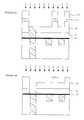
- FIGS. 1 (A-J)is a cross sectional view showing a damascene process flow for fabricating an interconnect structure.
- a process for the formation of electrical interconnect lines between different layers in a semiconductor deviceis described.
- the processovercomes a number of problems noted in the prior art.
- the processemploys a low k dielectric bilayer that does not result in pullback of the dielectric film or cause an increase in the effective k value of the dielectric film.
- lithographic patterning of photoresists on the dielectric bilayerresults in well defined feature.
- the processprovides novel RIE chemistry that provides high etch selectivity and CD control.
- the RIE processcan be adapted to selectively strip or ash residual photoresist and post etch residues.
- FIGS. 1 (A-J)there is depicted a dual damascene process flow suitable for practicing the present invention.
- the illustrated dual damascene process flowis exemplary only. It is understood that a variety of damascene process strategies could be used.
- the substrate 10may be a semiconductor wafer or chip which is composed of any Si-containing semiconductor material such as, but not limited to Si, SiGe, Si/SiGe, silicon-on-insulator and other like Si containing semiconductor materials.
- the substratemay be of the n- or p-type depending on the desired device to be fabricated.
- the substratemay contain various isolation and/or device regions formed in the substrate or on a surface thereof.
- the substratemay also contain metallic pads on the surface thereof. For clarity, the above mentioned regions and metallic pads are not shown in the drawings, but are nevertheless meant to be included with the substrate.
- the substratemay also be a circuit that includes CMOS devices therein, or alternatively, substrate may be one of the interconnect levels of the interconnect structure.
- the first conductor layer 12includes a completed metal interconnect and a dielectric layer.
- An optional thin capping layer 14 of silicon nitride, silicon oxycarbide, silicon oxynitride, silicon nitride carbide, silicon carbide or the likeis deposited onto the first metal layer.
- the dielectric capping layer 14if needed, generally serves as, among others, an etch stop, an adhesion promoter for copper metal deposition and also provides protection to the underlying first metal layer 12 . i.e., a barrier layer.
- a bilayer dielectric structurecomprising a first layer 16 and a second layer 18 is formed or deposited onto the etch stop layer 14 .
- the first layer 16is selected to have a higher dielectric constant than the second layer 18 .
- the first layeris silicon dioxide.
- the dielectric constant of silicon dioxideis about 4.0.
- the silicon dioxide layeris preferably deposited using standard plasma enhanced chemical vapor deposition (PECVD) or high density plasma chemical vapor deposition (HDP CVD) processes generally known to those in the art.
- the first layer 16may instead comprise a hybrid dielectric structure, such as those hybrid structures described in U.S. patent Ser. No. 09/596,750, now U.S. Pat. No. 6,548,901, herein incorporated by reference in its entirety.
- the second layer 18is preferably a low k dielectric film containing Si, C, O, and H and has a dielectric constant less than then first layer.
- the dielectric constantis less than or about 3.5.
- the second layer 18is a nonpolymeric hydrogenated oxidized silicon carbon layer (SiCOH) having a dielectric constant of about 2.7 to about 2.9. Hydrogenated oxidized silicon carbon and processes for deposition thereof are generally described in U.S. Pat. No. 6,147,009 to Grill et al., herein incorporated by reference in its entirety.
- the second layeri.e., hydrogenated oxidized silicon carbon layer
- the second layeris deposited by PECVD or HDP CVD from a gas mixture containing an organosilicon precursor gas and an oxygen-providing gas, which are substantially free from nitrogen.
- the precursor gascontains at least one organosilicon compound having a ring structure.
- Suitable organosilicon precursor gasesinclude molecules with ring structures such as 1,3,5,7-tetramethylcyclotetrasiloxane (TMCTS, or C 4 H 16 O 4 Si 4 ), tetraethylcyclotetrasiloxane (C 8 H 24 O 4 Si 4 ), or decamethylcyclopentasiloxane (C 10 H 30 O 5 Si 5 ) or other cyclic methyl siloxanes.
- TCTS1,3,5,7-tetramethylcyclotetrasiloxane
- C 8 H 24 O 4 Si 4tetraethylcyclotetrasiloxane
- decamethylcyclopentasiloxaneC 10 H 30 O 5 Si 5
- other precursorscomprising Si, C, O and H containing gases that are substantially free from nitrogen may also be used.
- Such precursorsmay be selected from the group of methylsilanes, such as tetramethylsilane (Si(CH 3 ) 4 ), or trimethylsilane (SiH(CH 3 ) 3 ).
- the oxygen-providing gasincludes those compounds that contain oxygen.
- the oxygen providing gasis selected from the group consisting of oxygen, carbon monoxide, carbon dioxide, water vapor, ozone and mixtures thereof.
- a photoresist layer 20is coated onto the second dielectric layer 18 , selectively patterned by exposure to activating energy and subsequently developed to form a relief image in the photoresist.
- the relief imageincludes the formation of a via 21 that exposes a portion of the second dielectric layer 18 .
- viaor “contact” refers to vias, trenches, grooves, contact holes, and the like in a substrate.
- footingmay be caused by a chemical interaction occurring at an interface between the exposed regions of photoresist and the underlying layer.
- the exposed regionscontain catalytic amounts of acid for providing a solubility differential during subsequent development between the exposed and unexposed regions of photoresist. Neutralization of the acid at the interface can lead to footing and/or prolonged exposure times
- DUV photoresistsare optimized for exposure to radiation having a wavelength at about 248 nm.
- DUV photoresist formulationstypically include a binder resin and a photoacid generator (PAG).
- the binder resinsare typically modified polyvinyl phenol polymers or polyvinylphenol/acrylate copolymers in which the phenol or carboxylate groups are partially “blocked” or protected by moieties which can be chemically cleaved.
- these systemsare based on an acid catalyzed mechanism wherein a strong acid is generated upon exposure of activating energy to a photoacid generator compound present in the photoresist formulation. A dissolution differential then exists between exposed (deprotected polymer) and unexposed (protected polymer) regions. It is this catalytic mechanism that is primarily responsible for the high sensitivity of these systems.
- Photoresists optimized for exposure to radiation at 193 nmemploy a variety of other protected polymers that necessarily contain few or no aromatic groups due to the strong absorption of 193 nm light to aromatic compounds.
- some of these photoresistsare based on acrylate polymers having various non-aromatic functional groups. Similar to DUV photoresists, these resists also utilize an amplification mechanism.
- the PAG chemistry of 193 nm resistsis essentially the same as that of DUV resists.
- the footing phenomena of photoresistsis especially problematic with low k dielectrics formed by PECVD from a gas mixture including a nitrogen containing gas.
- a nitrogen containing gascan create free amine groups within the resulting dielectric structure.
- the free amine groupscan interact at the interface with the catalytic amount of acid generated upon exposure of the photoresist to activating energy, thereby neutralizing some of the acid.
- subsequent development of the photoresistfails to remove or clear the amine poisoned areas resulting in footing.
- the use of the second layer 18 as describedadvantageously results in improved critical dimension (CD) control.
- CDcritical dimension
- the sidewalls of the via profilesare vertical and importantly, the dielectric/photoresist interface exhibits no footing.
- an anisotropic etching processis performed to etch away the exposed portion of the second dielectric layer 18 until the silicon dioxide layer 16 is exposed.
- the anisotropic etching processis a reactive ion etching process. This step can be performed using commercially available reactive ion etch/downstream microwave plasma ashing systems.
- the removal of the second dielectric layer 18is performed with a gas mixture containing CHF 3 , CF 4 , O 2 and argon, wherein the total pressure of all four gases is between about 5 millitorr (mT) and about 500 mT.
- the flow rate of CHF 3is provided at about 20 standard cubic centimeters per minute (sccm)
- CF 4is provided at a flow rate of about 60 sccm
- O 2is provided at a flow rate of about 5 sccm
- argonis at about 400 sccm.
- the power levelis maintained between about 100 Watts (W) and about 3000 W.
- the reactive ion etchis performed at a temperature of about 20° C. for a period of about 2 minutes.
- a dual frequency powermay be employed using two RF generators, each powered between about 100 and about 2000 watts.
- the reactive ion etching process parameters discussed hereinrefer to 200 mm sized wafers. As wafers scale from 200 mm to 300 mm, the flows and powers mentioned herein are expected to scale as well. Those skilled in the art will be able to optimize the process parameters for 300 mm sized wafers in view of this disclosure.
- the substrateis exposed to a different RIE chemistry selective for selectively removing the first dielectric layer 16 , i.e, silicon dioxide.
- the selective removal of the SiO 2 layer 16is performed in the same apparatus described above used to perform the removal of the second dielectric layer 18 , i.e., the SiCOH layer.
- an atmosphere comprising carbon monoxide (CO), C 4 F 8 , O 2 and argon having a total pressure of between about 10 to about 200 mTis established. More preferably, a total pressure of about 28 mT is established.
- the flow rates for the gasesare as follows: CO is at about 100 sccm, C 4 F 8 is at about 6 sccm, O 2 is at about 5 sccm and argon is at about 100 sccm.
- the power usedis maintained at about 3500 W at a temperature of about 20° C. until the first layer 16 is removed to the etch stop layer 14 as determined using standard methods known to those of skill in the semiconductor fabrication arts.
- each generatorwill be powered between 100 and 2000 W.
- the resulting viahas a high aspect ratio preferably between about 10:1 to less than about 1:1. More preferably, the resulting aspect ratio is about 3:1.
- residual photoresist, polymers and etch residuesare removed by a plasma-mediated stripping or ashing process.
- the photoresist, polymers and etch residuesare removed in the same apparatus as described above.
- a high density plasma reactive ion etching processHDP RIE
- the plasmais formed from a gas mixture including C 2 H 4 , O 2 and nitrogen atmosphere having a total pressure between about 1 to about 100 mT. More preferably, the total pressure is about 10 mT.
- a flow rate for C 2 H 4is between about 5 to about 20 sccm; more preferably, the flow rate is about 11 sccm.
- a flow rate for O 2is between about 10 to about 50 sccm; more preferably, the flow rate is about 20 sccm.
- a flow rate for nitrogenis between about 10 to about 200 sccm; more preferably, the flow rate is about 80 sccm.
- the power level usedis maintained at a level between about 200 to about 2000 W, more preferably about 800 W with a plasma frequency between about 50 to about 500 Megahertz (MHz) and more preferably, from about about 1.6 to about 27 MHz.
- the processingis continued for a period of about 3 minutes at a temperature of about 20° C.
- the use of ethyleneprotects the sidewalls of the via during the stripping process and maintains the critical dimension within tightly controlled specifications.
- ethylene gasforms a polymer on the sidewall during the photoresist mask removal.
- hydrocarbonsmay be used in addition to ethylene or in place of ethylene. Suitable hydrocarbons include methane, acetylene, C 4 H 8 , cyclic alkene, alkene or the like.
- the hydrocarbonsare a gas or vapor under plasma forming conditions.
- a high density plasma (HDP) RIEis generated from a gas mixture including SO 2 , O 2 and Ar at about 10 mT.
- a flow rate for SO 2is less than about 60 sccm, with a flow rate of about 20 sccm preferred.
- a flow rate for O 2is less than about 60 sccm, with a flow rate of about 20 sccm preferred.
- the flow rateis less than 500 sccm with a flow rate somewhat greater than 0 sccm preferred, i.e., a trickle amount.
- the power level usedis maintained at a level between about 100 W to about 1000 W, with about 260 W source preferred, a bias from about 10 W to about 500 W with about 80 W preferred, and a plasma frequency of about 1.6 MHz to about 2.7 MHz, with about 13.56 MHz preferred.
- the processingis continued for a period of about 1.5 minutes at a temperature of about 10° C.
- the plasmais formed from a gas mixture including forming gas (4% H 2 in N 2 ), CF 4 and oxygen at 1000 mT.
- a flow rate for the forming gasis from about 100 to about 10000 sccm, with about 5000 sccm preferred.
- a flow rate for CF 4is less than about 1000 sccm, with about 100 sccm preferred.
- the flow rateis somewhat greater than about 0 sccm.
- the power level usedis maintained at a level from about 500 W to about 2500 W, with about 900 W preferred and a plasma frequency of about 13.56 Megahertz (MHz).
- the processingis continued for a period of about 30 seconds at a temperature of about 250° C.
- the stepmay first be run without CF 4 for 1 to 3 minutes and then switched to the above named N 2 —H 2 /CF 4 plasma.
- the plasmais formed from a gas mixture of N 2 , H 2 , NH 3 or forming gas (10% H 2 in N 2 ), CF 4 and oxygen at a total pressure between about 20 to about 1000 mT.
- a flow rate for the gas mixtureis between about 100 to about 2000 sccm.
- the power level usedis maintained at a level between about 200 to about 2000 W.
- the processingis continued for a period of about 3 minutes at a temperature of about 0° C.
- the photoresist stripping processis highly selective.
- the critical dimension of the viais substantially unchanged after stripping.
- a planarizing layer 22 of an anti-reflective coating (ARC)is formed on the substrate surface.
- a photoresist layer 24is subsequently coated and patterned to form the line-level, e.g., a trench feature 25 , using photolithographic techniques.
- the substrate 10is exposed to an etching process for removing a portion of the second layer 18 to form the line level.
- a selective anisotropic RIE processis used to remove the exposed regions of ARC on the substrate.
- the selective RIE plasmauses a gas mixture containing N 2 , O 2 , and CO at about 18 millitorr (mT).
- a flow rate for the N 2 gasis between about 10 to about 1000 sccm, for O 2 gas is between about 5 to about 50 sccm and for CO gas, it is between about 10 to about 200 sccm.
- the flow rate for the N 2 gasis about 100 sccm, for O 2 gas at about 20 sccm and for CO gas at about 30 sccm.
- the power level usedis maintained at a level between about 200 to about 1500 watts for a period of about 45 to about 180 seconds at a temperature of about 20° C.
- a portion of the second layer 18 (SiCOH)is removed.
- the depth of removalis preferably time-based.
- the RIE plasmais generated from a gas mixture containing CHF 3 , CF 4 , O 2 and argon, wherein the total pressure of all four gases is about 60 mT.
- the flow rate of CHF 3is provided at about 20 sccm
- CF 4is provided at a flow rate of about 60 sccm
- O 2is provided at a flow rate of about 5 sccm
- argonis at about 400 sccm.
- the power levelis maintained between about 100 W and about 2000 W. If using a dual frequency power source, each generator is maintained between about 100 W and about 2000 W.
- the reactive ion etchis performed at a temperature of about 20° C. for a period of about 30 seconds.
- the selective RIE plasmauses a gas mixture containing forming gas at 100 mT.
- a flow rate for the forming gas (10% hydrogen in nitrogen)is at about 500 sccm.
- the power level usedis maintained at a level between about 100 W to 2000 W with a plasma frequency of about 13.56 to about 60 MHz.
- the processingis continued for a period of about 30 seconds at a temperature of about 20° C. to remove a portion of the anti-reflective layer to the second layer 18 .
- a portion of the second layer 18SiCOH
- the inventionis not intended to be limited to forming gas.
- Other hydrogen gas and noble gas combinationsincluding N 2 , H 2 , NH 3 , N 2 H 2 , Ar, He, Xe, Kr or the like may be utilized.
- FIG. 1Hresidual photoresist, residual ARC, polymers and post-etch residues are selectively removed from the substrate using one of the plasma mediated ashing processes as previously described in FIG. 1 E.
- the dielectric capping layer 14is selectively removed.
- a RIE process for removing the layeris generated from a gas mixture containing CHF 3 , O 2 and argon at about 12 mT.
- a flow rate for CHF 3is at about 12 sccm, for O 2 at about 10 sccm and for argon at about 425 sccm.
- the power level usedis maintained at a level between about 500 W to about 2000 W with a plasma frequency of about 1.6 to about 13.56 Megahertz (MHz). More preferably, the power level is at about 800 W and the plasma frequency is maintained between about 1.6 to about 2.2 MHz.
- a copper metal deposition processis used to fill the spaces left by the etching and stripping process to form the second metal layer.
- Current copper deposition techniquesrequire the deposition of a barrier layer that also acts as a seed layer for subsequent copper deposition. After the copper has been deposited, the wafer surface is then planarized typically by a chemical mechanical polishing step. A barrier layer 26 is then deposited and the above described processes are repeated. In this manner, the integrated circuit or the like is formed.
Landscapes
- Engineering & Computer Science (AREA)
- General Physics & Mathematics (AREA)
- Physics & Mathematics (AREA)
- Condensed Matter Physics & Semiconductors (AREA)
- Manufacturing & Machinery (AREA)
- Computer Hardware Design (AREA)
- Microelectronics & Electronic Packaging (AREA)
- Power Engineering (AREA)
- Chemical & Material Sciences (AREA)
- General Chemical & Material Sciences (AREA)
- Chemical Kinetics & Catalysis (AREA)
- Inorganic Chemistry (AREA)
- Drying Of Semiconductors (AREA)
- Internal Circuitry In Semiconductor Integrated Circuit Devices (AREA)
Abstract
Description
Claims (20)
Priority Applications (1)
| Application Number | Priority Date | Filing Date | Title |
|---|---|---|---|
| US09/994,340US6649531B2 (en) | 2001-11-26 | 2001-11-26 | Process for forming a damascene structure |
Applications Claiming Priority (1)
| Application Number | Priority Date | Filing Date | Title |
|---|---|---|---|
| US09/994,340US6649531B2 (en) | 2001-11-26 | 2001-11-26 | Process for forming a damascene structure |
Publications (2)
| Publication Number | Publication Date |
|---|---|
| US20030100190A1 US20030100190A1 (en) | 2003-05-29 |
| US6649531B2true US6649531B2 (en) | 2003-11-18 |
Family
ID=25540554
Family Applications (1)
| Application Number | Title | Priority Date | Filing Date |
|---|---|---|---|
| US09/994,340Expired - LifetimeUS6649531B2 (en) | 2001-11-26 | 2001-11-26 | Process for forming a damascene structure |
Country Status (1)
| Country | Link |
|---|---|
| US (1) | US6649531B2 (en) |
Cited By (48)
| Publication number | Priority date | Publication date | Assignee | Title |
|---|---|---|---|---|
| US20030186537A1 (en)* | 2002-03-27 | 2003-10-02 | Matsushita Electric Industrial Co., Ltd. | Method for fabricating electronic device |
| US20030207563A1 (en)* | 1998-11-25 | 2003-11-06 | Smith Patricia B. | Method for photoresist strip, sidewall polymer removal and passivation for aluminum metallization |
| US20040155012A1 (en)* | 2003-02-12 | 2004-08-12 | Lam Research Corporation | Methods of reducing photoresist distortion while etching in a plasma processing system |
| US20040161924A1 (en)* | 2003-02-14 | 2004-08-19 | Jei-Ming Chen | Damascene interconnect with bilayer capping film |
| US20050239278A1 (en)* | 2004-04-27 | 2005-10-27 | Agency For Science, Technology And Research | Process of forming a composite diffusion barrier in copper/organic low-k damascene technology |
| US20050260845A1 (en)* | 2004-05-21 | 2005-11-24 | Texas Instruments Incorporated | Low-K dielectric etch process for dual-damascene structures |
| US20050287790A1 (en)* | 2002-10-30 | 2005-12-29 | Fujitsu Limited | Silicon oxycarbide, growth method of silicon oxycarbide layer, semiconductor device and manufacture method for semiconductor device |
| US7030041B2 (en)* | 2004-03-15 | 2006-04-18 | Applied Materials Inc. | Adhesion improvement for low k dielectrics |
| US20060105576A1 (en)* | 2004-11-18 | 2006-05-18 | International Business Machines Corporation | High ion energy and reative species partial pressure plasma ash process |
| US7049249B2 (en) | 2003-01-13 | 2006-05-23 | Applied Materials | Method of improving stability in low k barrier layers |
| US7091137B2 (en) | 2001-12-14 | 2006-08-15 | Applied Materials | Bi-layer approach for a hermetic low dielectric constant layer for barrier applications |
| US7157384B2 (en) | 2001-12-14 | 2007-01-02 | Applied Materials, Inc. | Low dielectric (low k) barrier films with oxygen doping by plasma-enhanced chemical vapor deposition (PECVD) |
| US20070023806A1 (en)* | 2005-07-29 | 2007-02-01 | International Business Machines Corporation | Method and structure for forming slot via bitline for MRAM devices |
| US20070049007A1 (en)* | 2005-08-31 | 2007-03-01 | International Business Machines Corporation | Interconnect structure and method for forming the same |
| US7229911B2 (en) | 2004-04-19 | 2007-06-12 | Applied Materials, Inc. | Adhesion improvement for low k dielectrics to conductive materials |
| US7288205B2 (en) | 2004-07-09 | 2007-10-30 | Applied Materials, Inc. | Hermetic low dielectric constant layer for barrier applications |
| US20080038934A1 (en)* | 2006-04-18 | 2008-02-14 | Air Products And Chemicals, Inc. | Materials and methods of forming controlled void |
| US20080044992A1 (en)* | 2006-08-21 | 2008-02-21 | Hynix Semiconductor Inc. | Method for fabricating a recess gate in a semiconductor device |
| SG142201A1 (en)* | 2006-11-07 | 2008-05-28 | United Microelectronics Corp | Method for fabricating a dual damascene structure |
| US20080132067A1 (en)* | 2006-11-30 | 2008-06-05 | Hong Ma | Method for fabricating a dual damascene structure |
| US20080153247A1 (en)* | 2006-12-26 | 2008-06-26 | Hynix Semiconductor Inc. | Method For Manufacturing Semiconductor Device |
| US20080207002A1 (en)* | 2007-02-27 | 2008-08-28 | International Business Machines Corporation | Method of removing graphitic and/or fluorinated organic layers from the surface of a chip passivation layer having si-containing compounds |
| US20080303160A1 (en)* | 2004-03-13 | 2008-12-11 | Colburn Matthew E | Method for fabricating dual damascene structures using photo-imprint lithography, methods for fabricating imprint lithography molds for dual damascene structures, materials for imprintable dielectrics and equipment for photo-imprint lithography used in dual damascene patterning |
| US20090081418A1 (en)* | 2007-09-20 | 2009-03-26 | International Business Machines Corporation | Spin-on antireflective coating for integration of patternable dielectric materials and interconnect structures |
| US20090079076A1 (en)* | 2007-09-20 | 2009-03-26 | International Business Machines Corporation | Patternable dielectric film structure with improved lithography and method of fabricating same |
| US20090079075A1 (en)* | 2007-09-20 | 2009-03-26 | International Business Machines Corporation | Interconnect structures with patternable low-k dielectrics and method of fabricating same |
| US20090315186A1 (en)* | 2008-06-20 | 2009-12-24 | Nec Electronics Corporation | Method for manufacturing semiconductor device and the semiconductor device |
| US7749563B2 (en) | 2002-10-07 | 2010-07-06 | Applied Materials, Inc. | Two-layer film for next generation damascene barrier application with good oxidation resistance |
| US20120115303A1 (en)* | 2010-11-08 | 2012-05-10 | International Business Machines Corporation | Method of fabricating damascene structures |
| US8232198B2 (en) | 2010-08-05 | 2012-07-31 | International Business Machines Corporation | Self-aligned permanent on-chip interconnect structure formed by pitch splitting |
| US8367540B2 (en) | 2009-11-19 | 2013-02-05 | International Business Machines Corporation | Interconnect structure including a modified photoresist as a permanent interconnect dielectric and method of fabricating same |
| US8399359B2 (en) | 2011-06-01 | 2013-03-19 | United Microelectronics Corp. | Manufacturing method for dual damascene structure |
| US8450212B2 (en) | 2011-06-28 | 2013-05-28 | International Business Machines Corporation | Method of reducing critical dimension process bias differences between narrow and wide damascene wires |
| US8518832B1 (en) | 2011-06-27 | 2013-08-27 | Western Digital (Fremont), Llc | Process for masking and removal of residue from complex shapes |
| US8647991B1 (en) | 2012-07-30 | 2014-02-11 | United Microelectronics Corp. | Method for forming dual damascene opening |
| US8703397B1 (en) | 2012-03-29 | 2014-04-22 | Western Digital (Fremont), Llc | Method for providing side shields for a magnetic recording transducer |
| US8735295B2 (en) | 2012-06-19 | 2014-05-27 | United Microelectronics Corp. | Method of manufacturing dual damascene structure |
| US8822137B2 (en) | 2011-08-03 | 2014-09-02 | International Business Machines Corporation | Self-aligned fine pitch permanent on-chip interconnect structures and method of fabrication |
| US20140308817A1 (en)* | 2013-04-16 | 2014-10-16 | Tokyo Electron Limited | Etching method |
| US8890318B2 (en) | 2011-04-15 | 2014-11-18 | International Business Machines Corporation | Middle of line structures |
| US8900988B2 (en) | 2011-04-15 | 2014-12-02 | International Business Machines Corporation | Method for forming self-aligned airgap interconnect structures |
| US8921226B2 (en) | 2013-01-14 | 2014-12-30 | United Microelectronics Corp. | Method of forming semiconductor structure having contact plug |
| US8962490B1 (en) | 2013-10-08 | 2015-02-24 | United Microelectronics Corp. | Method for fabricating semiconductor device |
| US9001467B1 (en) | 2014-03-05 | 2015-04-07 | Western Digital (Fremont), Llc | Method for fabricating side shields in a magnetic writer |
| US9054160B2 (en) | 2011-04-15 | 2015-06-09 | International Business Machines Corporation | Interconnect structure and method for fabricating on-chip interconnect structures by image reversal |
| US20150348892A1 (en)* | 2014-05-28 | 2015-12-03 | United Microelectronics Corp. | Interposer fabricating process and wafer packaging structure |
| US9236298B2 (en) | 2011-09-08 | 2016-01-12 | Globalfoundries Inc. | Methods for fabrication interconnect structures with functional components and electrical conductive contact structures on a same level |
| US9299847B2 (en) | 2012-05-10 | 2016-03-29 | Globalfoundries Inc. | Printed transistor and fabrication method |
Families Citing this family (13)
| Publication number | Priority date | Publication date | Assignee | Title |
|---|---|---|---|---|
| US20030213617A1 (en)* | 2002-05-20 | 2003-11-20 | Subramanian Karthikeyan | Method and structure of a reducing intra-level and inter-level capacitance of a semiconductor device |
| GB2394879B (en)* | 2002-11-04 | 2005-11-23 | Electrolux Outdoor Prod Ltd | Trimmer |
| US20040219790A1 (en)* | 2003-04-30 | 2004-11-04 | Wilson Aaron R | Etching methods, RIE methods, and methods of increasing the stability of photoresist during RIE |
| JP2006024670A (en)* | 2004-07-07 | 2006-01-26 | Sony Corp | Manufacturing method of semiconductor device |
| US9318378B2 (en)* | 2004-08-21 | 2016-04-19 | Globalfoundries Singapore Pte. Ltd. | Slot designs in wide metal lines |
| US20060086690A1 (en)* | 2004-10-21 | 2006-04-27 | Ming-Huan Tsai | Dielectric etching method to prevent photoresist damage and bird's beak |
| US20070243714A1 (en)* | 2006-04-18 | 2007-10-18 | Applied Materials, Inc. | Method of controlling silicon-containing polymer build up during etching by using a periodic cleaning step |
| US7815815B2 (en) | 2006-08-01 | 2010-10-19 | Sony Corporation | Method and apparatus for processing the peripheral and edge portions of a wafer after performance of a surface treatment thereon |
| US8435419B2 (en)* | 2010-06-14 | 2013-05-07 | Applied Materials, Inc. | Methods of processing substrates having metal materials |
| KR101973077B1 (en) | 2012-01-18 | 2019-04-29 | 삼성디스플레이 주식회사 | Method of manufacturing trench, metal wire, and thin film transistor array panel |
| US11037798B2 (en)* | 2016-11-09 | 2021-06-15 | Tokyo Electron Limited | Self-limiting cyclic etch method for carbon-based films |
| US10453684B1 (en)* | 2018-05-09 | 2019-10-22 | Applied Materials, Inc. | Method for patterning a material layer with desired dimensions |
| CN114284208B (en)* | 2021-12-20 | 2024-10-18 | 武汉新芯集成电路股份有限公司 | Method for manufacturing semiconductor device |
Citations (17)
| Publication number | Priority date | Publication date | Assignee | Title |
|---|---|---|---|---|
| US4099999A (en)* | 1977-06-13 | 1978-07-11 | Xerox Corporation | Method of making etched-striped substrate planar laser |
| JPS547275A (en) | 1977-06-18 | 1979-01-19 | Nippon Telegr & Teleph Corp <Ntt> | X-ray mask support and its manufacture |
| JPH06296340A (en) | 1993-04-09 | 1994-10-21 | Hitachi Ltd | Rotating electric machine |
| US5661083A (en) | 1996-01-30 | 1997-08-26 | Integrated Device Technology, Inc. | Method for via formation with reduced contact resistance |
| JPH09304023A (en) | 1996-05-21 | 1997-11-28 | Hitachi Ltd | Sample size measuring device |
| US5710079A (en) | 1996-05-24 | 1998-01-20 | Lsi Logic Corporation | Method and apparatus for forming dielectric films |
| US5770523A (en) | 1996-09-09 | 1998-06-23 | Taiwan Semiconductor Manufacturing Company, Ltd. | Method for removal of photoresist residue after dry metal etch |
| US5861064A (en) | 1997-03-17 | 1999-01-19 | Fsi Int Inc | Process for enhanced photoresist removal in conjunction with various methods and chemistries |
| US5902702A (en) | 1996-05-15 | 1999-05-11 | Mitsubishi Denki Kabushiki Kaisha | Phase shift mask, blank for phase shift mask, and method of manufacturing phase shift mask |
| US5970376A (en) | 1997-12-29 | 1999-10-19 | Taiwan Semiconductor Manufacturing Company, Ltd. | Post via etch plasma treatment method for forming with attenuated lateral etching a residue free via through a silsesquioxane spin-on-glass (SOG) dielectric layer |
| US6013582A (en) | 1997-12-08 | 2000-01-11 | Applied Materials, Inc. | Method for etching silicon oxynitride and inorganic antireflection coatings |
| US6017817A (en)* | 1999-05-10 | 2000-01-25 | United Microelectronics Corp. | Method of fabricating dual damascene |
| US6080529A (en) | 1997-12-12 | 2000-06-27 | Applied Materials, Inc. | Method of etching patterned layers useful as masking during subsequent etching or for damascene structures |
| US6097095A (en) | 1999-06-09 | 2000-08-01 | Alliedsignal Inc. | Advanced fabrication method of integrated circuits with borderless vias and low dielectric-constant inter-metal dielectrics |
| US6350700B1 (en)* | 2000-06-28 | 2002-02-26 | Lsi Logic Corporation | Process for forming trenches and vias in layers of low dielectric constant carbon-doped silicon oxide dielectric material of an integrated circuit structure |
| US6372635B1 (en)* | 2001-02-06 | 2002-04-16 | Advanced Micro Devices, Inc. | Method for making a slot via filled dual damascene low k interconnect structure without middle stop layer |
| US6429121B1 (en)* | 2001-02-07 | 2002-08-06 | Advanced Micro Devices, Inc. | Method of fabricating dual damascene with silicon carbide via mask/ARC |
- 2001
- 2001-11-26USUS09/994,340patent/US6649531B2/ennot_activeExpired - Lifetime
Patent Citations (17)
| Publication number | Priority date | Publication date | Assignee | Title |
|---|---|---|---|---|
| US4099999A (en)* | 1977-06-13 | 1978-07-11 | Xerox Corporation | Method of making etched-striped substrate planar laser |
| JPS547275A (en) | 1977-06-18 | 1979-01-19 | Nippon Telegr & Teleph Corp <Ntt> | X-ray mask support and its manufacture |
| JPH06296340A (en) | 1993-04-09 | 1994-10-21 | Hitachi Ltd | Rotating electric machine |
| US5661083A (en) | 1996-01-30 | 1997-08-26 | Integrated Device Technology, Inc. | Method for via formation with reduced contact resistance |
| US5902702A (en) | 1996-05-15 | 1999-05-11 | Mitsubishi Denki Kabushiki Kaisha | Phase shift mask, blank for phase shift mask, and method of manufacturing phase shift mask |
| JPH09304023A (en) | 1996-05-21 | 1997-11-28 | Hitachi Ltd | Sample size measuring device |
| US5710079A (en) | 1996-05-24 | 1998-01-20 | Lsi Logic Corporation | Method and apparatus for forming dielectric films |
| US5770523A (en) | 1996-09-09 | 1998-06-23 | Taiwan Semiconductor Manufacturing Company, Ltd. | Method for removal of photoresist residue after dry metal etch |
| US5861064A (en) | 1997-03-17 | 1999-01-19 | Fsi Int Inc | Process for enhanced photoresist removal in conjunction with various methods and chemistries |
| US6013582A (en) | 1997-12-08 | 2000-01-11 | Applied Materials, Inc. | Method for etching silicon oxynitride and inorganic antireflection coatings |
| US6080529A (en) | 1997-12-12 | 2000-06-27 | Applied Materials, Inc. | Method of etching patterned layers useful as masking during subsequent etching or for damascene structures |
| US5970376A (en) | 1997-12-29 | 1999-10-19 | Taiwan Semiconductor Manufacturing Company, Ltd. | Post via etch plasma treatment method for forming with attenuated lateral etching a residue free via through a silsesquioxane spin-on-glass (SOG) dielectric layer |
| US6017817A (en)* | 1999-05-10 | 2000-01-25 | United Microelectronics Corp. | Method of fabricating dual damascene |
| US6097095A (en) | 1999-06-09 | 2000-08-01 | Alliedsignal Inc. | Advanced fabrication method of integrated circuits with borderless vias and low dielectric-constant inter-metal dielectrics |
| US6350700B1 (en)* | 2000-06-28 | 2002-02-26 | Lsi Logic Corporation | Process for forming trenches and vias in layers of low dielectric constant carbon-doped silicon oxide dielectric material of an integrated circuit structure |
| US6372635B1 (en)* | 2001-02-06 | 2002-04-16 | Advanced Micro Devices, Inc. | Method for making a slot via filled dual damascene low k interconnect structure without middle stop layer |
| US6429121B1 (en)* | 2001-02-07 | 2002-08-06 | Advanced Micro Devices, Inc. | Method of fabricating dual damascene with silicon carbide via mask/ARC |
Non-Patent Citations (1)
| Title |
|---|
| Ruth DeJule, "Dual-Damascene: Overcoming Process Issues", Jun. 2000,"www.semiconductor.net." |
Cited By (87)
| Publication number | Priority date | Publication date | Assignee | Title |
|---|---|---|---|---|
| US20030207563A1 (en)* | 1998-11-25 | 2003-11-06 | Smith Patricia B. | Method for photoresist strip, sidewall polymer removal and passivation for aluminum metallization |
| US7157384B2 (en) | 2001-12-14 | 2007-01-02 | Applied Materials, Inc. | Low dielectric (low k) barrier films with oxygen doping by plasma-enhanced chemical vapor deposition (PECVD) |
| US7091137B2 (en) | 2001-12-14 | 2006-08-15 | Applied Materials | Bi-layer approach for a hermetic low dielectric constant layer for barrier applications |
| US7022619B2 (en)* | 2002-03-27 | 2006-04-04 | Matsushita Electric Industrial Co., Ltd. | Method for fabricating electronic device |
| US20030186537A1 (en)* | 2002-03-27 | 2003-10-02 | Matsushita Electric Industrial Co., Ltd. | Method for fabricating electronic device |
| US7749563B2 (en) | 2002-10-07 | 2010-07-06 | Applied Materials, Inc. | Two-layer film for next generation damascene barrier application with good oxidation resistance |
| US7485570B2 (en)* | 2002-10-30 | 2009-02-03 | Fujitsu Limited | Silicon oxycarbide, growth method of silicon oxycarbide layer, semiconductor device and manufacture method for semiconductor device |
| US20050287790A1 (en)* | 2002-10-30 | 2005-12-29 | Fujitsu Limited | Silicon oxycarbide, growth method of silicon oxycarbide layer, semiconductor device and manufacture method for semiconductor device |
| US7049249B2 (en) | 2003-01-13 | 2006-05-23 | Applied Materials | Method of improving stability in low k barrier layers |
| US6942816B2 (en)* | 2003-02-12 | 2005-09-13 | Lam Research Corporation | Methods of reducing photoresist distortion while etching in a plasma processing system |
| WO2004073025A3 (en)* | 2003-02-12 | 2005-03-03 | Lam Res Comporation | Methods of reducing photoresist distortion while etching in a plasma processing system |
| US20040155012A1 (en)* | 2003-02-12 | 2004-08-12 | Lam Research Corporation | Methods of reducing photoresist distortion while etching in a plasma processing system |
| US6873057B2 (en)* | 2003-02-14 | 2005-03-29 | United Microelectrtonics Corp. | Damascene interconnect with bi-layer capping film |
| US20040161924A1 (en)* | 2003-02-14 | 2004-08-19 | Jei-Ming Chen | Damascene interconnect with bilayer capping film |
| US7982312B2 (en)* | 2004-03-13 | 2011-07-19 | International Business Machines Corporation | Method for fabricating dual damascene structures using photo-imprint lithography, methods for fabricating imprint lithography molds for dual damascene structures, materials for imprintable dielectrics and equipment for photo-imprint lithography used in dual damascene patterning |
| US20080303160A1 (en)* | 2004-03-13 | 2008-12-11 | Colburn Matthew E | Method for fabricating dual damascene structures using photo-imprint lithography, methods for fabricating imprint lithography molds for dual damascene structures, materials for imprintable dielectrics and equipment for photo-imprint lithography used in dual damascene patterning |
| US7030041B2 (en)* | 2004-03-15 | 2006-04-18 | Applied Materials Inc. | Adhesion improvement for low k dielectrics |
| US7459404B2 (en) | 2004-03-15 | 2008-12-02 | Applied Materials, Inc. | Adhesion improvement for low k dielectrics |
| US7229911B2 (en) | 2004-04-19 | 2007-06-12 | Applied Materials, Inc. | Adhesion improvement for low k dielectrics to conductive materials |
| US7335990B2 (en)* | 2004-04-27 | 2008-02-26 | Agency For Science, Technology And Research | Process of forming a composite diffusion barrier in copper/organic low-k damascene technology |
| US7244674B2 (en)* | 2004-04-27 | 2007-07-17 | Agency For Science Technology And Research | Process of forming a composite diffusion barrier in copper/organic low-k damascene technology |
| US20070252278A1 (en)* | 2004-04-27 | 2007-11-01 | Chaoyong Li | Process of forming a composite diffusion barrier in copper/organic low-k damascene technology |
| US20050239278A1 (en)* | 2004-04-27 | 2005-10-27 | Agency For Science, Technology And Research | Process of forming a composite diffusion barrier in copper/organic low-k damascene technology |
| US7192877B2 (en)* | 2004-05-21 | 2007-03-20 | Texas Instruments Incorporated | Low-K dielectric etch process for dual-damascene structures |
| US20050260845A1 (en)* | 2004-05-21 | 2005-11-24 | Texas Instruments Incorporated | Low-K dielectric etch process for dual-damascene structures |
| US7288205B2 (en) | 2004-07-09 | 2007-10-30 | Applied Materials, Inc. | Hermetic low dielectric constant layer for barrier applications |
| US7253116B2 (en) | 2004-11-18 | 2007-08-07 | International Business Machines Corporation | High ion energy and reative species partial pressure plasma ash process |
| US20060105576A1 (en)* | 2004-11-18 | 2006-05-18 | International Business Machines Corporation | High ion energy and reative species partial pressure plasma ash process |
| US7635884B2 (en) | 2005-07-29 | 2009-12-22 | International Business Machines Corporation | Method and structure for forming slot via bitline for MRAM devices |
| US20090302405A1 (en)* | 2005-07-29 | 2009-12-10 | International Business Machines Corporation | Method for forming slot via bitline for mram devices |
| US7825420B2 (en)* | 2005-07-29 | 2010-11-02 | International Business Machines Corporation | Method for forming slot via bitline for MRAM devices |
| US20070023806A1 (en)* | 2005-07-29 | 2007-02-01 | International Business Machines Corporation | Method and structure for forming slot via bitline for MRAM devices |
| US7727888B2 (en)* | 2005-08-31 | 2010-06-01 | International Business Machines Corporation | Interconnect structure and method for forming the same |
| US20070049007A1 (en)* | 2005-08-31 | 2007-03-01 | International Business Machines Corporation | Interconnect structure and method for forming the same |
| US20080038934A1 (en)* | 2006-04-18 | 2008-02-14 | Air Products And Chemicals, Inc. | Materials and methods of forming controlled void |
| US8399349B2 (en)* | 2006-04-18 | 2013-03-19 | Air Products And Chemicals, Inc. | Materials and methods of forming controlled void |
| US8846522B2 (en) | 2006-04-18 | 2014-09-30 | Air Products And Chemicals, Inc. | Materials and methods of forming controlled void |
| US7557030B2 (en)* | 2006-08-21 | 2009-07-07 | Hynix Semiconductor Inc. | Method for fabricating a recess gate in a semiconductor device |
| US20080044992A1 (en)* | 2006-08-21 | 2008-02-21 | Hynix Semiconductor Inc. | Method for fabricating a recess gate in a semiconductor device |
| SG142201A1 (en)* | 2006-11-07 | 2008-05-28 | United Microelectronics Corp | Method for fabricating a dual damascene structure |
| US7510965B2 (en) | 2006-11-30 | 2009-03-31 | United Microelectronics Corp. | Method for fabricating a dual damascene structure |
| US20080132067A1 (en)* | 2006-11-30 | 2008-06-05 | Hong Ma | Method for fabricating a dual damascene structure |
| US7585780B2 (en)* | 2006-12-26 | 2009-09-08 | Hynix Semiconductor Inc. | Method for manufacturing semiconductor device |
| US20080153247A1 (en)* | 2006-12-26 | 2008-06-26 | Hynix Semiconductor Inc. | Method For Manufacturing Semiconductor Device |
| US20080207002A1 (en)* | 2007-02-27 | 2008-08-28 | International Business Machines Corporation | Method of removing graphitic and/or fluorinated organic layers from the surface of a chip passivation layer having si-containing compounds |
| US7938976B2 (en)* | 2007-02-27 | 2011-05-10 | International Business Machines Corporation | Method of removing graphitic and/or fluorinated organic layers from the surface of a chip passivation layer having Si-containing compounds |
| US7709370B2 (en) | 2007-09-20 | 2010-05-04 | International Business Machines Corporation | Spin-on antireflective coating for integration of patternable dielectric materials and interconnect structures |
| US7944055B2 (en) | 2007-09-20 | 2011-05-17 | International Business Machines Corporation | Spin-on antireflective coating for integration of patternable dielectric materials and interconnect structures |
| US20090079075A1 (en)* | 2007-09-20 | 2009-03-26 | International Business Machines Corporation | Interconnect structures with patternable low-k dielectrics and method of fabricating same |
| US8084862B2 (en) | 2007-09-20 | 2011-12-27 | International Business Machines Corporation | Interconnect structures with patternable low-k dielectrics and method of fabricating same |
| US20090081418A1 (en)* | 2007-09-20 | 2009-03-26 | International Business Machines Corporation | Spin-on antireflective coating for integration of patternable dielectric materials and interconnect structures |
| US8618663B2 (en) | 2007-09-20 | 2013-12-31 | International Business Machines Corporation | Patternable dielectric film structure with improved lithography and method of fabricating same |
| US9484248B2 (en) | 2007-09-20 | 2016-11-01 | Globalfoundries Inc. | Patternable dielectric film structure with improved lithography and method of fabricating same |
| US8450854B2 (en) | 2007-09-20 | 2013-05-28 | International Business Machines Corporation | Interconnect structures with patternable low-k dielectrics and method of fabricating same |
| US20090079076A1 (en)* | 2007-09-20 | 2009-03-26 | International Business Machines Corporation | Patternable dielectric film structure with improved lithography and method of fabricating same |
| US20090315186A1 (en)* | 2008-06-20 | 2009-12-24 | Nec Electronics Corporation | Method for manufacturing semiconductor device and the semiconductor device |
| US8008777B2 (en)* | 2008-06-20 | 2011-08-30 | Renesas Electronics Corporation | Method for manufacturing semiconductor device and the semiconductor device |
| US9431295B2 (en) | 2009-11-19 | 2016-08-30 | Globalfoundries Inc. | Interconnect structure including a modified photoresist as a permanent interconnect dielectric and method of fabricating same |
| US8367540B2 (en) | 2009-11-19 | 2013-02-05 | International Business Machines Corporation | Interconnect structure including a modified photoresist as a permanent interconnect dielectric and method of fabricating same |
| US8232198B2 (en) | 2010-08-05 | 2012-07-31 | International Business Machines Corporation | Self-aligned permanent on-chip interconnect structure formed by pitch splitting |
| US8795556B2 (en) | 2010-08-05 | 2014-08-05 | International Business Machines Corporation | Self-aligned permanent on-chip interconnect structure formed by pitch splitting |
| US8293638B2 (en)* | 2010-11-08 | 2012-10-23 | International Business Machines Corporation | Method of fabricating damascene structures |
| US20120115303A1 (en)* | 2010-11-08 | 2012-05-10 | International Business Machines Corporation | Method of fabricating damascene structures |
| US9490202B2 (en) | 2011-04-15 | 2016-11-08 | GlobalFoundries, Inc. | Self-aligned airgap interconnect structures |
| US8890318B2 (en) | 2011-04-15 | 2014-11-18 | International Business Machines Corporation | Middle of line structures |
| US9343354B2 (en) | 2011-04-15 | 2016-05-17 | Globalfoundries Inc. | Middle of line structures and methods for fabrication |
| US9245791B2 (en) | 2011-04-15 | 2016-01-26 | Globalfoundries Inc. | Method for fabricating a contact |
| US9054160B2 (en) | 2011-04-15 | 2015-06-09 | International Business Machines Corporation | Interconnect structure and method for fabricating on-chip interconnect structures by image reversal |
| US8900988B2 (en) | 2011-04-15 | 2014-12-02 | International Business Machines Corporation | Method for forming self-aligned airgap interconnect structures |
| US8399359B2 (en) | 2011-06-01 | 2013-03-19 | United Microelectronics Corp. | Manufacturing method for dual damascene structure |
| US8518832B1 (en) | 2011-06-27 | 2013-08-27 | Western Digital (Fremont), Llc | Process for masking and removal of residue from complex shapes |
| US8450212B2 (en) | 2011-06-28 | 2013-05-28 | International Business Machines Corporation | Method of reducing critical dimension process bias differences between narrow and wide damascene wires |
| US8822137B2 (en) | 2011-08-03 | 2014-09-02 | International Business Machines Corporation | Self-aligned fine pitch permanent on-chip interconnect structures and method of fabrication |
| US9209126B2 (en) | 2011-08-03 | 2015-12-08 | Globalfoundries Inc. | Self-aligned fine pitch permanent on-chip interconnect structures and method of fabrication |
| US9236298B2 (en) | 2011-09-08 | 2016-01-12 | Globalfoundries Inc. | Methods for fabrication interconnect structures with functional components and electrical conductive contact structures on a same level |
| US8703397B1 (en) | 2012-03-29 | 2014-04-22 | Western Digital (Fremont), Llc | Method for providing side shields for a magnetic recording transducer |
| US9299847B2 (en) | 2012-05-10 | 2016-03-29 | Globalfoundries Inc. | Printed transistor and fabrication method |
| US8735295B2 (en) | 2012-06-19 | 2014-05-27 | United Microelectronics Corp. | Method of manufacturing dual damascene structure |
| US8647991B1 (en) | 2012-07-30 | 2014-02-11 | United Microelectronics Corp. | Method for forming dual damascene opening |
| US8921226B2 (en) | 2013-01-14 | 2014-12-30 | United Microelectronics Corp. | Method of forming semiconductor structure having contact plug |
| US9105585B2 (en)* | 2013-04-16 | 2015-08-11 | Tokyo Electron Limited | Etching method |
| US20140308817A1 (en)* | 2013-04-16 | 2014-10-16 | Tokyo Electron Limited | Etching method |
| US8962490B1 (en) | 2013-10-08 | 2015-02-24 | United Microelectronics Corp. | Method for fabricating semiconductor device |
| US9001467B1 (en) | 2014-03-05 | 2015-04-07 | Western Digital (Fremont), Llc | Method for fabricating side shields in a magnetic writer |
| US20150348892A1 (en)* | 2014-05-28 | 2015-12-03 | United Microelectronics Corp. | Interposer fabricating process and wafer packaging structure |
| US9466560B2 (en)* | 2014-05-28 | 2016-10-11 | United Microelectronics Corp. | Interposer fabricating process and wafer packaging structure |
| US9929081B2 (en)* | 2014-05-28 | 2018-03-27 | United Microelectronics Corp. | Interposer fabricating process |
Also Published As
| Publication number | Publication date |
|---|---|
| US20030100190A1 (en) | 2003-05-29 |
Similar Documents
| Publication | Publication Date | Title |
|---|---|---|
| US6649531B2 (en) | Process for forming a damascene structure | |
| US6207583B1 (en) | Photoresist ashing process for organic and inorganic polymer dielectric materials | |
| US7235478B2 (en) | Polymer spacer formation | |
| US6740566B2 (en) | Ultra-thin resist shallow trench process using high selectivity nitride etch | |
| US6720132B2 (en) | Bi-layer photoresist dry development and reactive ion etch method | |
| US7390749B2 (en) | Self-aligned pitch reduction | |
| US6638875B2 (en) | Oxygen free plasma stripping process | |
| US8470708B2 (en) | Double patterning strategy for contact hole and trench in photolithography | |
| US6787452B2 (en) | Use of amorphous carbon as a removable ARC material for dual damascene fabrication | |
| US7399712B1 (en) | Method for etching organic hardmasks | |
| US7067235B2 (en) | Bi-layer photoresist dry development and reactive ion etch method | |
| US6936533B2 (en) | Method of fabricating semiconductor devices having low dielectric interlayer insulation layer | |
| JP5122106B2 (en) | Carbon-containing film etching method and semiconductor device manufacturing method using the same | |
| US7351635B2 (en) | Method of fabricating microelectronic device using super critical fluid | |
| US7291553B2 (en) | Method for forming dual damascene with improved etch profiles | |
| WO2003081665A1 (en) | Process for producing semiconductor device and semiconductor device | |
| US20050032354A1 (en) | Method for selectively controlling damascene CD bias | |
| US7189643B2 (en) | Semiconductor device and method of fabricating the same | |
| US6858542B2 (en) | Semiconductor fabrication method for making small features | |
| US6787455B2 (en) | Bi-layer photoresist method for forming high resolution semiconductor features | |
| US6875699B1 (en) | Method for patterning multilevel interconnects | |
| US7192880B2 (en) | Method for line etch roughness (LER) reduction for low-k interconnect damascene trench etching | |
| JP4651956B2 (en) | Interlayer dielectric film dry etching method | |
| JP4681217B2 (en) | Interlayer dielectric film dry etching method | |
| US6613665B1 (en) | Process for forming integrated circuit structure comprising layer of low k dielectric material having antireflective properties in an upper surface |
Legal Events
| Date | Code | Title | Description |
|---|---|---|---|
| AS | Assignment | Owner name:INTERNATIONAL BUSINESS MACHINES CORPORATION, NEW Y Free format text:ASSIGNMENT OF ASSIGNORS INTEREST;ASSIGNORS:COTE, WILLIAM J.;DALTON, TIMOTHY J.;DEV, PRAKASH CHIMANLAL;AND OTHERS;REEL/FRAME:012327/0463;SIGNING DATES FROM 20010926 TO 20011120 Owner name:INFINEON TECHNOLOGIES NORTH AMERICA CORP., CALIFOR Free format text:ASSIGNMENT OF ASSIGNORS INTEREST;ASSIGNOR:LEE, GILL YONG;REEL/FRAME:012327/0625 Effective date:20011009 | |
| STCF | Information on status: patent grant | Free format text:PATENTED CASE | |
| FEPP | Fee payment procedure | Free format text:PAYOR NUMBER ASSIGNED (ORIGINAL EVENT CODE: ASPN); ENTITY STATUS OF PATENT OWNER: LARGE ENTITY | |
| AS | Assignment | Owner name:INFINEON TECHNOLOGIES AG, GERMANY Free format text:ASSIGNMENT OF ASSIGNORS INTEREST;ASSIGNOR:INFINEON TECHNOLOGIES NORTH AMERICA CORP.;REEL/FRAME:015871/0170 Effective date:20050407 | |
| FPAY | Fee payment | Year of fee payment:4 | |
| AS | Assignment | Owner name:QIMONDA AG, GERMANY Free format text:ASSIGNMENT OF ASSIGNORS INTEREST;ASSIGNOR:INFINEON TECHNOLOGIES AG;REEL/FRAME:023788/0535 Effective date:20060425 | |
| FPAY | Fee payment | Year of fee payment:8 | |
| AS | Assignment | Owner name:INFINEON TECHNOLOGIES AG, GERMANY Free format text:ASSIGNMENT OF ASSIGNORS INTEREST;ASSIGNOR:QIMONDA AG;REEL/FRAME:035623/0001 Effective date:20141009 | |
| FPAY | Fee payment | Year of fee payment:12 | |
| SULP | Surcharge for late payment | Year of fee payment:11 | |
| AS | Assignment | Owner name:GLOBALFOUNDRIES U.S. 2 LLC, NEW YORK Free format text:ASSIGNMENT OF ASSIGNORS INTEREST;ASSIGNOR:INTERNATIONAL BUSINESS MACHINES CORPORATION;REEL/FRAME:036550/0001 Effective date:20150629 | |
| AS | Assignment | Owner name:GLOBALFOUNDRIES INC., CAYMAN ISLANDS Free format text:ASSIGNMENT OF ASSIGNORS INTEREST;ASSIGNORS:GLOBALFOUNDRIES U.S. 2 LLC;GLOBALFOUNDRIES U.S. INC.;REEL/FRAME:036779/0001 Effective date:20150910 | |
| AS | Assignment | Owner name:SAMSUNG ELECTRONICS CO., LTD., KOREA, REPUBLIC OF Free format text:ASSIGNMENT OF ASSIGNORS INTEREST;ASSIGNOR:INFINEON TECHNOLOGIES AG;REEL/FRAME:037221/0885 Effective date:20150930 | |
| AS | Assignment | Owner name:WILMINGTON TRUST, NATIONAL ASSOCIATION, DELAWARE Free format text:SECURITY AGREEMENT;ASSIGNOR:GLOBALFOUNDRIES INC.;REEL/FRAME:049490/0001 Effective date:20181127 | |
| AS | Assignment | Owner name:GLOBALFOUNDRIES U.S. INC., CALIFORNIA Free format text:ASSIGNMENT OF ASSIGNORS INTEREST;ASSIGNOR:GLOBALFOUNDRIES INC.;REEL/FRAME:054633/0001 Effective date:20201022 | |
| AS | Assignment | Owner name:GLOBALFOUNDRIES INC., CAYMAN ISLANDS Free format text:RELEASE BY SECURED PARTY;ASSIGNOR:WILMINGTON TRUST, NATIONAL ASSOCIATION;REEL/FRAME:054636/0001 Effective date:20201117 | |
| AS | Assignment | Owner name:GLOBALFOUNDRIES U.S. INC., NEW YORK Free format text:RELEASE BY SECURED PARTY;ASSIGNOR:WILMINGTON TRUST, NATIONAL ASSOCIATION;REEL/FRAME:056987/0001 Effective date:20201117 |