US6646697B1 - Liquid crystal display - Google Patents
Liquid crystal displayDownload PDFInfo
- Publication number
- US6646697B1 US6646697B1US09/254,937US25493799AUS6646697B1US 6646697 B1US6646697 B1US 6646697B1US 25493799 AUS25493799 AUS 25493799AUS 6646697 B1US6646697 B1US 6646697B1
- Authority
- US
- United States
- Prior art keywords
- liquid crystal
- crystal display
- polarizing film
- display panel
- reflection
- Prior art date
- Legal status (The legal status is an assumption and is not a legal conclusion. Google has not performed a legal analysis and makes no representation as to the accuracy of the status listed.)
- Expired - Lifetime
Links
Images


Classifications
- G—PHYSICS
- G04—HOROLOGY
- G04G—ELECTRONIC TIME-PIECES
- G04G9/00—Visual time or date indication means
- G04G9/0023—Visual time or date indication means by light valves in general
- G04G9/0029—Details
- G04G9/0035—Details constructional
- G—PHYSICS
- G02—OPTICS
- G02F—OPTICAL DEVICES OR ARRANGEMENTS FOR THE CONTROL OF LIGHT BY MODIFICATION OF THE OPTICAL PROPERTIES OF THE MEDIA OF THE ELEMENTS INVOLVED THEREIN; NON-LINEAR OPTICS; FREQUENCY-CHANGING OF LIGHT; OPTICAL LOGIC ELEMENTS; OPTICAL ANALOGUE/DIGITAL CONVERTERS
- G02F1/00—Devices or arrangements for the control of the intensity, colour, phase, polarisation or direction of light arriving from an independent light source, e.g. switching, gating or modulating; Non-linear optics
- G02F1/01—Devices or arrangements for the control of the intensity, colour, phase, polarisation or direction of light arriving from an independent light source, e.g. switching, gating or modulating; Non-linear optics for the control of the intensity, phase, polarisation or colour
- G02F1/13—Devices or arrangements for the control of the intensity, colour, phase, polarisation or direction of light arriving from an independent light source, e.g. switching, gating or modulating; Non-linear optics for the control of the intensity, phase, polarisation or colour based on liquid crystals, e.g. single liquid crystal display cells
- G02F1/133—Constructional arrangements; Operation of liquid crystal cells; Circuit arrangements
- G02F1/1333—Constructional arrangements; Manufacturing methods
- G02F1/1347—Arrangement of liquid crystal layers or cells in which the final condition of one light beam is achieved by the addition of the effects of two or more layers or cells
- G02F1/13471—Arrangement of liquid crystal layers or cells in which the final condition of one light beam is achieved by the addition of the effects of two or more layers or cells in which all the liquid crystal cells or layers remain transparent, e.g. FLC, ECB, DAP, HAN, TN, STN, SBE-LC cells
- G—PHYSICS
- G02—OPTICS
- G02F—OPTICAL DEVICES OR ARRANGEMENTS FOR THE CONTROL OF LIGHT BY MODIFICATION OF THE OPTICAL PROPERTIES OF THE MEDIA OF THE ELEMENTS INVOLVED THEREIN; NON-LINEAR OPTICS; FREQUENCY-CHANGING OF LIGHT; OPTICAL LOGIC ELEMENTS; OPTICAL ANALOGUE/DIGITAL CONVERTERS
- G02F1/00—Devices or arrangements for the control of the intensity, colour, phase, polarisation or direction of light arriving from an independent light source, e.g. switching, gating or modulating; Non-linear optics
- G02F1/01—Devices or arrangements for the control of the intensity, colour, phase, polarisation or direction of light arriving from an independent light source, e.g. switching, gating or modulating; Non-linear optics for the control of the intensity, phase, polarisation or colour
- G02F1/13—Devices or arrangements for the control of the intensity, colour, phase, polarisation or direction of light arriving from an independent light source, e.g. switching, gating or modulating; Non-linear optics for the control of the intensity, phase, polarisation or colour based on liquid crystals, e.g. single liquid crystal display cells
- G02F1/133—Constructional arrangements; Operation of liquid crystal cells; Circuit arrangements
- G02F1/1333—Constructional arrangements; Manufacturing methods
- G02F1/1335—Structural association of cells with optical devices, e.g. polarisers or reflectors
- G02F1/133528—Polarisers
- G02F1/133536—Reflective polarizers
- G—PHYSICS
- G02—OPTICS
- G02F—OPTICAL DEVICES OR ARRANGEMENTS FOR THE CONTROL OF LIGHT BY MODIFICATION OF THE OPTICAL PROPERTIES OF THE MEDIA OF THE ELEMENTS INVOLVED THEREIN; NON-LINEAR OPTICS; FREQUENCY-CHANGING OF LIGHT; OPTICAL LOGIC ELEMENTS; OPTICAL ANALOGUE/DIGITAL CONVERTERS
- G02F1/00—Devices or arrangements for the control of the intensity, colour, phase, polarisation or direction of light arriving from an independent light source, e.g. switching, gating or modulating; Non-linear optics
- G02F1/01—Devices or arrangements for the control of the intensity, colour, phase, polarisation or direction of light arriving from an independent light source, e.g. switching, gating or modulating; Non-linear optics for the control of the intensity, phase, polarisation or colour
- G02F1/13—Devices or arrangements for the control of the intensity, colour, phase, polarisation or direction of light arriving from an independent light source, e.g. switching, gating or modulating; Non-linear optics for the control of the intensity, phase, polarisation or colour based on liquid crystals, e.g. single liquid crystal display cells
- G02F1/133—Constructional arrangements; Operation of liquid crystal cells; Circuit arrangements
- G02F1/1333—Constructional arrangements; Manufacturing methods
- G02F1/1335—Structural association of cells with optical devices, e.g. polarisers or reflectors
- G02F1/133528—Polarisers
- G02F1/133545—Dielectric stack polarisers
Definitions
- the present inventionrelates to a liquid crystal display device used to display time information for a timepiece such as hours, minutes, and seconds and calendar information such as date, a day of the week, month, and year in digital form, using a liquid crystal display panel, or to display information from a microcomputer, a memo or the like, or to display information upon receiving a signal from the outside.
- the liquid crystal display panel in the liquid crystal display device used for these electronic machines and devicescan be broadly classified into two groups. One includes liquid crystal display panels using a polarizing film and the other includes types of liquid crystal display panels not using a polarizing film.
- the present inventionrelates to a liquid crystal display panel using a combination of a liquid crystal cell with a polarizing film.
- this kind of liquid crystal display deviceperforms display by voltage control of the transmission and absorption of light through a liquid crystal layer and a polarizing film.
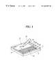
- FIG. 17is a perspective view of a conventional liquid crystal display device used to perform the display of data.
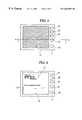
- FIG. 18is a schematic sectional view taken along the line 18 — 18 in FIG. 17 .
- FIG. 19is an enlarged sectional view of a portion in the liquid crystal display panel in FIG. 18 .
- a liquid crystal display panel 300 used in this liquid crystal display deviceincludes, in order from the side of glass 2 shown in FIG. 18 (the side visible to a viewer), a first substrate 11 , a first electrode 12 , a second substrate 13 facing the first substrate 11 at a predetermined distance, and a second electrode 14 provided on the second substrate 13 , wherein a portion where the first electrode 12 and the second electrode 14 overlap one another serves as a display pixel.
- the first electrode 12 and the second electrode 14are striped electrodes and are in a matrix-type display pixel arrangement.
- a liquid crystal layer 15exists between the first substrate 11 and the second substrate 13 , and the liquid crystal layer 15 is sealed with a sealing agent 33 and a sealant.
- An alignment layeris provided on the first substrate 11 and the second substrate 13 to align the liquid crystal layer 15 in a predetermined direction.
- the liquid crystal layer 15aligns in the direction corresponding to the time 7:30 on the first substrate 11 side, and the time 4:30 on the second substrate 13 , and has a twist angle of 90°.
- a super twisted nematic liquid crystal having an enlarged twist angle from 210° to 260°is sometimes used.
- a first polarizing film 21consists of an absorption-type polarizing film on which a coloring agent is spread in the one direction is provided on the first substrate 11
- a second polarizing film 22consists of, for example, DBEF (trade name) made by Sumitomo 3M Co., Ltd. is provided as a reflection-type polarizing film on the second substrate 12 .
- the transmission axes of the first polarizing film 21 and the second polarizing film 22are disposed parallel with each other and by combination with a liquid crystal panel, a strong reflection state can be shown when the voltage applied to the liquid crystal layer 15 is low, and a transmission state can be shown when the applied voltage is high.
- a light source 7consisting of an electroluminescent element (EL) is provided below the liquid crystal display panel 300 , and a printed circuit board 5 to apply a predetermined voltage to the liquid crystal display panel 300 and the light source 7 is provided.
- ELelectroluminescent element
- an integrated circuit (IC) 96comprising a driver circuit to drive a liquid crystal display panel is provided and a flexible printed circuit (FPC) 36 is used to connect the printed circuit board 5 and the liquid crystal display panel.
- ICintegrated circuit
- FPCflexible printed circuit
- the printed circuit board 5 and the light source 7are connected through a terminal for a light source (not shown).
- the liquid crystal display panel 300is held with a panel stopper, and is connected to the printed circuit board 5 and the like with a circuit board stopper holding the printed circuit board 5 and the like.
- a battery 6is connected by means of a battery stopping spring 38 .
- a liquid crystal display device moduleconsisting of the liquid crystal display panel 300 and the printed circuit board 5 is housed in the inside of a case 1 of the liquid crystal display device, having a glass 2 and a case back 3 .
- the liquid crystal display device having such a structurehas a display section 41 shown in FIG. 17, and the display section 41 has a input-letter display section 48 which makes it possible to input on the liquid crystal display panel with an input-pen 10 .
- the liquid crystal display devicealso has a series of control switches to display information necessary to a viewer.
- the liquid crystal display deviceis provided with buttons such as scroll (+), ( ⁇ ) buttons 51 and 52 to scroll the display, a display mode shifting button 53 , and an electric power switch 54 and with a speaker 40 for acoustic information.
- buttonssuch as scroll (+), ( ⁇ ) buttons 51 and 52 to scroll the display, a display mode shifting button 53 , and an electric power switch 54 and with a speaker 40 for acoustic information.
- These control switch or buttonsare mounted on a switch board 70 shown in FIG. 18 and are connected with the printed circuit board 5 through a FPC 71 .
- the display of only the data aloneimparts a monotonous design, and further lacks an interesting feature, which leads to loss of popularity among customers.
- a method of shielding (opening and closing of a shutter) a portion or all of the data-display section of the liquid crystal display device in accordance with circumstances at the time of use or internal condition of the liquid crystal display devicehas been studied, but it can not be said sufficient with regard to making the liquid crystal display device thinner and controllable.
- a time-display sectioncan be performed by a liquid crystal display device user, a timer, or a signal from the outside through communication, or that display or no display of information can be carried out by using a portion of the time-display section itself as a shutter.
- a liquid crystal display device usera timer, or a signal from the outside through communication
- display or no display of informationcan be carried out by using a portion of the time-display section itself as a shutter.
- a liquid crystal display deviceis comprised of laminated plural liquid crystal display panels, each of which comprises a liquid crystal layer filled in a gap between a pair of transparent substrates which provide an electrode on each opposing inner surface, and a reflection-type polarizing film which transmits the light linearly polarized in the direction parallel to the transmission axis thereof and reflects the light linearly polarized in the direction orthogonal to the transmission axis thereof, is disposed on at least any surface among the top surface of the plural liquid crystal display panels, between liquid crystal display panels, and the bottom surface of the plural liquid crystal display panels.
- two of the above described liquid crystal display panelsare laminated in such a manner that at least a portion thereof is overlaped each other, and the above described reflection-type polarizing film may be disposed at any one position among the top surface of the two laminated liquid crystal display panels, between the two laminated liquid crystal display panels, and the bottom surface thereof.
- each one of the two liquid crystal display panelshas an inner substrate facing the other liquid crystal display panel and an outer substrate placed opposite the other liquid crystal display panel, and the reflective-type polarizing film is disposed between the inner substrates of the two liquid crystal display panels.
- the reflection-type polarizing filmis preferably disposed in such a manner that the reflection-type polarizing film is adhered to the inner substrate of one of the liquid crystal display panels and a predetermined gap is provided between the reflective-type polarizing film and the inner substrate of the other liquid crystal display panel.
- the gap between the above described reflection-type polarizing film and the inner substrate of the other liquid crystal display panelcan be formed with a printed layer provided around the display area of the liquid crystal display panel.
- a liquid crystal display devicecan be structured in such a manner that two of the above structured liquid crystal display panels are laminated so that at least a portion thereof is respectively overlaped each other, and a first polarizing film is disposed on the top surface of the two laminated liquid crystal display panels, a second polarizing film is disposed between the two liquid crystal display panels, and a third polarizing film is on the bottom surface, respectively.
- a plurality of the above-described reflection-type polarizing filmscan be disposed.
- the top surface of the laminated two liquid crystal display panelsis placed on the visible side, and that the first polarizing film is an absorption-type polarizing film to transmit the light linearly polarized in the direction parallel to a transmission axis thereof but to absorb the light linearly polarized in the direction orthogonal to the transmission axis thereof, the second polarizing film is a reflection-type polarizing film, and the third polarizing film is a combination of a light-diffusion layer and the reflection-type polarizing film.
- the first polarizing film, the second polarizing film, and the above described liquid crystal display panel disposed in betweenare arranged to have a high transmission characteristic, as opposed to having a high reflection characteristic, in relation to a viewer side, when a voltage applied to the liquid crystal display panel is increased.
- first polarizing film, the second polarizing film, and the liquid crystal display panel disposed in betweenare arranged to have a high reflection characteristic, as opposed to having a high transmission characteristic, in relation to the viewer side, when a voltage applied to the liquid crystal display panel is increased.
- a liquid crystal display devicein a liquid crystal display device according to the invention, two liquid crystal display panels structured as described above are laminated in such a manner that at least a portion respectively of the two liquid crystal panel is overlaped each other, a first polarizing film is disposed on the upper surface of the first liquid crystal display panel disposed on the viewer side of the laminated two liquid crystal display panels, a second polarizing film is disposed between the first liquid crystal display panel and the second liquid crystal display panel, that is the other liquid crystal display panel, and the third polarizing film is disposed on the bottom surface of the above described second liquid crystal panel, respectively.
- the first liquid crystal display panelhas a plurality of segment display sections, and when the display shows a high transmission characteristic with the first polarizing film, the second polarizing film and the first liquid crystal display panel, the portion between each segment display section of the first liquid crystal display panel has a steady section in which a high reflection characteristic is constantly maintained when no voltage is applied to the liquid crystal layer.
- the second liquid crystal display panelhas a display pixel consisting of a matrix-type electrode structure.
- the display pixel of the second liquid crystal display panelis smaller than the above-described steady section, and a font size displayed by the second liquid crystal display panel can be made larger than the steady section of the first liquid crystal display panel.
- a reflection-type polarizing filmis disposed between the first liquid crystal display panel and the second liquid crystal display panel, an optical power-generating element which generates electric power on exposure to light is disposed on the bottom side of the second liquid crystal display panel, viewed through the polarizing film, and the display is performed on the first liquid crystal display panel or on the second liquid crystal display panel by means of light having a wavelength area contributing to the power generation of the optical power-generating element so that the electric power generated by the optical power-generating element can be used for power to drive the first and second liquid crystal display panels.
- a light scattering layeris preferably disposed between the optical power-generating element and the second liquid crystal display panel.
- a light-wavelength conversion layerwhich absorbs short wavelength light and emits long wavelength light, can be arranged between the above described optical power-generating element and the second liquid crystal display panel.
- a liquid crystal display devicehas at least any one of a sensor which detects a control signal generated by a viewer (user), a sensor to detect the circumstances of use, and a sensor to detect the time at which the liquid crystal display device displays, and a ratio of light incident on the transmission axis of the reflection-type polarizing film to light incident on the reflection axis intersecting the transmission axis at right angles can be varied by the liquid crystal display panel in accordance with a signal output by the sensor.
- a sensor which detects a radio wave signal existing in the applied circumstancemay also be provided, and in accordance with the signal detected by the sensor and an output signal therefrom, a ratio of light incident on the transmission axis to the light incident on the reflection axis orthogonal to the transmission axis can be varied by the liquid crystal display panel.
- the liquid crystal display panelcan be driven in synchronization with the light source.
- a fluorescent ink layerwhich emits light by absorbing light and changing the wavelength thereof can be provided on any place among the light source, on the polarizing film in the lowest layer, or between the above described light source and the polarizing film.
- a light-diffusion layerconsisting of a spacer on at least any one of the bottom side and the top side of the above described reflection-type polarizing film so that the reflection-type polarizing film and a opposing substrate form a gap with the spacer.
- FIG. 1is a perspective view of a liquid crystal display device showing a first embodiment of the present invention
- FIG. 2is a plane view showing a shutter-closed state of the liquid crystal display device
- FIG. 3is a plane view similarly showing a shutter-opened state
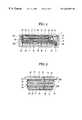
- FIG. 4is a schematic sectional view taken along the line 4 — 4 in FIG. 2, and
- FIG. 5is an enlarged sectional view of the liquid crystal display panel portion thereof in which a middle portion is broken away;
- FIG. 6is a system block diagram of the liquid crystal display device of the first embodiment of the present invention.
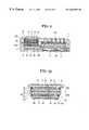
- FIG. 7is a schematic sectional view of a liquid crystal display device showing a second embodiment of the present invention.
- FIG. 8is an enlarged sectional view of the liquid crystal display panel portion thereof in which a middle portion is broken away;
- FIG. 9is a schematic sectional view of a liquid crystal display device showing a third embodiment of the present invention.
- FIG. 10is an enlarged sectional view of the liquid crystal display panel portion thereof in which the middle portion is broken away.
- FIG. 11is an enlarged sectional view of a liquid crystal display panel portion of a liquid crystal display device showing a fourth embodiment of the present invention, in which a middle portion is broken away;
- FIG. 12is an enlarged sectional view of a liquid crystal display panel portion of a liquid crystal display device showing a fifth embodiment of the present invention, in which a middle portion is broken away;
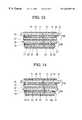
- FIG. 13is an enlarged sectional view of a liquid crystal display panel portion of a liquid crystal display device showing a sixth embodiment of the present invention, in which a middle portion is broken away;
- FIG. 14is an enlarged sectional view of a liquid crystal display panel portion of a liquid crystal display device showing a seventh embodiment of the present invention, in which a middle portion is broken away;
- FIG. 15is an enlarged sectional view of a liquid crystal display panel portion of a liquid crystal display device showing an eighth embodiment of the present invention, in which a middle portion is broken away;
- FIG. 16is an enlarged sectional view of a liquid crystal display panel portion of a liquid crystal display device showing a ninth embodiment of the present invention, in which a middle portion is broken away;
- FIG. 17is a perspective view showing an example of the conventional liquid crystal display device.
- FIG. 18is a schematic section al view taken along the line 18 — 18 in FIG. 17, and
- FIG. 19is an enlarged sectional view of the liquid crystal display panel portion in which a middle portion is broken away.
- the liquid crystal display device of the present inventionis provided with plural liquid crystal display panels which are laminated in such a manner that at least a portion of the display areas are overlaped each other respectively.
- a first liquid crystal display panel 100 and a second liquid crystal display panel 200are laminated so that most of the display area of each overlaps the other.
- the first liquid crystal display panel 100consists of a first substrate 11 , a first electrode 12 formed in the inner surface thereof, a second substrate 13 facing the first substrate 11 at a predetermined distance, and a second electrode 14 formed in the inside surface of the second substrate 13 , in order from the glass 2 side (side visible to a viewer).
- the first substrate 11 and the second substrate 13are transparent glass plates and on the inner facing surfaces of the substrate 11 and 13 , the first electrode 12 and the second electrode 14 are formed in predetermined patterns of indium tin oxide (ITO), a transparent conductive material.
- ITOindium tin oxide
- the display pixelhas a non-divided one-face electrode shape.
- a first liquid crystal layer 15is provided between the first substrate 11 and the second substrate 13 , contained therebetween by a sealing agent 33 and a sealant.
- An alignment layeris provided on the first substrate 11 , the second substrate 13 , and the first and second electrode 12 , 14 shown in FIG. 5, to align the first liquid crystal layer 15 in a predetermined direction.
- the liquid crystalsalign in the direction corresponding to the time 7:30 on the first substrate 11 , and the time 4:30 on the second substrate 13 , and the twist angle of the first liquid crystal layer 15 is 90°.
- first polarizing film 21consisting of an absorption-type polarizing film in which pigments are stretched in the one direction
- second polarizing film 22consisting of, for example, DBEF (trade name) manufactured by Sumitomo 3M Co., Ltd. as a reflection-type polarizing film.
- the first polarizing film 21 and the second polarizing film 22are arranged in such a manner that their transmission axes are parallel to each other, and in combination with the liquid crystal display panel 100 , they exhibit a strong reflective characteristic when voltage applied to the liquid crystal layer 15 is low, and exhibit a transmission characteristic when high voltage is applied.
- the second polarizing film 22is adhered on the second substrate 13 of the liquid crystal display panel 100 with an adhesive agent.
- the structure of the second liquid crystal display panel 200includes, in order from the glass 2 side (side visible to a viewer), a third substrate 16 , a third electrode 17 formed on the inside surface thereof, a fourth substrate 18 which faces the third substrate 16 at a predetermined distance, and a fourth electrode 19 formed on the inside surface thereof. Overlapping portions of the third electrodes 17 and the fourth electrodes 19 are display pixels.
- the third electrodes 17 and the fourth electrodes 19 of the second liquid crystal display panel 200form a shape of striped electrodes intersecting each other at right angles to be a matrix-form display pixel array.
- a second liquid crystal layer 20is provided and sealed therein by a sealing agent 33 and a sealant.
- an alignment layeris provided to align the second liquid crystal layer 20 in a predetermined direction.
- the second liquid crystal layer 20is aligned on the direction corresponding to the time 7:30 in the third substrate 16 side and the time 4:30 on the fourth substrate 18 side, and the twist angle is taken to be 90°. That is, the first liquid crystal layer 15 and the second liquid crystal layer 20 have the same alignment directions and the good viewing directions are the same.
- No polarizing filmis provided on the third substrate 16 and the second polarizing film 22 is used instead thereof, and an absorption-type polarizing film 23 is arranged as a third polarizing film on the fourth substrate 18 .
- the first polarizing film 21 and the second polarizing film 22are disposed in such a manner that their transmission axes intersect with each other, and by combining the liquid crystal display panels 100 and 200 , a high transmission characteristic is exhibited when low voltage is applied to the second liquid crystal layer 20 , and a high absorption characteristic is exhibited when high voltage is applied.
- a spacer 35is provided between the second polarizing film 22 and the third substrate 16 , and it has a structure to provide a gap so as to not allow at least the second polarizing film 22 to be in contact with the third substrate 16 . Further, a translucent reflecting film 25 which reflects more than 50% of light and transmits the remainder thereof is provided at the bottom surface of the third polarizing film 23 .
- a light source 7which consists of an electroluminescent (EL) element is disposed on the bottom of the second liquid crystal display panel 200 , and the printed circuit board 5 to apply a predetermined voltage to the first and second liquid crystal display panels 100 , 200 and the light source 7 is further provided.
- ELelectroluminescent
- the first liquid crystal panelis connected to the fourth substrate 18 of the second liquid crystal panel 200 . Then, they are in turn connected to the printed circuit board 5 through a flexible printed circuit (FPC) 37 attached to the fourth substrate 18 .
- FPCflexible printed circuit
- connection of the printed circuit board 5 with the second liquid crystal display panel 200is carried out by the face-down mounting on the fourth substrate 18 of a panel driver IC for driving the liquid crystal display panel, using a chip-on-glass method (COG) and connected through the FPC 37 .
- COGchip-on-glass method
- this structure of mountingcan be said to be a suitable mounting means for the first liquid crystal display panel 100 and the second liquid display panel 200 .
- the second polarizing film 22is adhered on the bottom surface of the second substrate 13 with an adhesive agent, and between the second polarizing film 22 and the third substrate 16 the spacer 35 made of plastic beads is spread.
- the second polarizing film 22is a reflection-type polarizing film, the occurrence of distortion in the second polarizing film 22 becomes visible even if it is a small distortion such as that which is invisible in the conventional absorption-type polarizing film.
- the occurrence of distortion in the second polarizing film 22lowers the display quality.
- the gap between the second polarizing film 22 and the third substrate 16depends on the uniformity of area and thickness between the second substrate 13 and the third substrate 16 , or the uniformity of thickness between the second polarizing film 22 and the adhesive layer. Since the size is limited in the case of the liquid crystal display device, the gap is limited by an amount of the sprayed plastic beads. If the amount of beads is greater than 10 pcs/mm 2 , the gap in a range between 5 to 100 micrometers ( ⁇ m) is suitable, and in a range between 10 to 50 micrometers ( ⁇ m) is more suitable to prevent the display quality of the second liquid crystal display panel 200 from lowering.
- interference fringesbreak out due to close proximity of the second polarizing film 22 with the third substrate 16 .
- the battery 6is fixed with a battery stopper 38 on the side wall of the printed circuit board 5 .
- a scroll up (+) botton 51 and a scroll down ( ⁇ ) button 52are provided to allow user input of commands, and the buttons or switches are connected to the printed circuit board 5 through a switch board 70 and a switch-use FPC 71 .
- liquid crystal display modulehaving a two-layer structure of the first liquid crystal display panel 100 and the second liquid crystal display panel 200 is assembled.
- the liquid crystal display devicethus structured has a shutter-display section 41 (FIG. 1 to FIG. 3) which consists of an undivided electrode structure having an area of the first liquid crystal display panel 100 larger than the area of the display section of the liquid crystal display panel 200 , and becomes a shutter display 44 which has an uniform display as shown in FIG. 2 and which shows a strong reflective characteristic when no voltage or low voltage is applied on the first liquid crystal layer 15 .
- a shutter-display section 41(FIG. 1 to FIG. 3) which consists of an undivided electrode structure having an area of the first liquid crystal display panel 100 larger than the area of the display section of the liquid crystal display panel 200 , and becomes a shutter display 44 which has an uniform display as shown in FIG. 2 and which shows a strong reflective characteristic when no voltage or low voltage is applied on the first liquid crystal layer 15 .
- the first liquid crystal display panel 100serves as a closed shutter to shield the display of the second liquid crystal display panel 200 .
- a schedule display 42 to show information in the memory IC and a shutter-control display 43are shown on the display section of the second liquid crystal display panel to be waiting a command to open or close of the shutter.
- the shutter function of the first liquid crystal display panel 100operates as shown in FIG. 1, and a change in shutter display 44 from a transmission state to a reflection state is displayed on a part of the display section, and a shutter-state display 47 in a secret (closing) operation is put on.
- the gap of the first liquid layer 15is made step-wise in this embodiment.
- the shuttertakes an open state with even a low voltage applied at the place where the gap of the first liquid crystal layer 15 is small.
- the shutterremains in a closed state until it reaches a high voltage condition.
- the voltage applied to the first liquid crystal display panel 100By making the voltage applied to the first liquid crystal display panel 100 higher, it is controlled to a state of transmittance over its entire area, and as shown in FIG. 3, all of the surface of the display section of the second liquid crystal display panel 200 can be seen as the shutter display section 41 is controlled to a full-open state.
- a pen-input type input deviceis provided on the glass 2 in this embodiment.
- the pen-input type input devicehas a pressure-sensitive system and an electromagnetic induction system, and the pressure-sensitive system is advantageous because of its portability and cost-performance.
- the methodis performed in a manner wherein two sheets of thin film substrate face each other divided by a spacer therebetween, and a high-resistance transparent conductive film is formed on each facing surface of the two sheets of the substrate and a position where the upper and lower transparent conductive films are brought into contact with each other by an applied pressure is computed from the resistance value.
- An information-generating means 92consists of a standard signal generating circuit 72 , a memory information circuit 75 , and an input information circuit 76 , and the standard signal generating circuit 72 is structured with a power source circuit 73 and a central processing circuit (CPU) 74 .
- the CPU 74performs each kind of signal processing based on a clock signal (several ten megaHz).
- a bidirectional processingis performed with the memory information circuit 75 or the input information circuit 76 , so that the information necessary for the display of the display device (the second liquid crystal display panel) 79 is supplied.
- Information from the memory information circuit 75 and the input information circuit 76is converted into a predetermined signal by a CPU 74 , transferred to a controller circuit 85 , outputted to a scanning signal generating circuit 77 and a data signal generating circuit 78 , and input to the display device 79 .
- memory informationinformation from pen-input type input device, shutter information and so on are displayed.
- a shutter display sectionthat is a display of the first liquid crystal display panel 100 will be explained.
- a switch signal output from a switching means 80is output as a control signal to a shutter controlling means 93 consisting of an open-close control circuit 81 to control a strong reflection state (shutter closing) and a full transmission state (shutter opening) on the display of the first liquid crystal display panel, and an open-close driving circuit 82 to drive a switch shutter device 83 that is the first liquid crystal display panel 100 .
- the switch means 80utilizes a signal inputted by a pen-input type input device in the first embodiment.
- a characteristic of the first embodimentis to provide the second polarizing film 22 between the first liquid crystal display panel 100 and the second liquid crystal display panel 200 , and the second polarizing film 22 is a reflection-type polarizing film which is adhered to the second substrate 13 .
- a predetermined gap filled by spacer made of spherical plastic beadsis provided between the second polarizing film 22 and the third substrate 16 , which prevents the occurrence of interference fringes caused by the second polarizing film 22 and the third substrate 16 , and makes it easy to position the first liquid crystal display panel and the second liquid crystal display panel.
- the power consumptioncan be adjusted as necessary.
- FIG. 7Second Embodiment: FIG. 7, FIG. 8
- FIG. 7 and FIG. 8a liquid crystal display device according to the second embodiment of the present invention will be explained with reference to FIG. 7 and FIG. 8 .
- the same reference numeralsare used to the same portion as these are used as in the explanation of the above described first embodiment in FIG. 4 and FIG. 5, and the explanation thereof is omitted.
- a feature different from the first embodimentis that a spacer 45 consisting of a printed layer is provided between the second substrate 13 and the second polarizing film 22 , and the second polarizing film 22 is adhered on the third substrate 16 .
- a diffusion layer 46 and the third polarizing film 23are disposed on the bottom side of the fourth substrate 18 .
- no glass 2is provided on the viewer side of the liquid crystal display device, the case 1 and the first substrate 11 have an equal surface height, and acrylic resin 88 is filled in the border portion of the first substrate 11 and the case 1 .
- a printed layer 89is provided on the first polarizing film 21 of the first substrate 11 and the case 1 .
- a reflection-type polarizing filmis used as the second polarizing film 22 and as the third polarizing film 23 .
- the first and second electrodes 12 , 14 of the first liquid crystal display panel 100are formed in a striped manner and are arranged such that the electrode stripes intersect with each other at right angles, and the display pixels are formed thereby in a matrix form at a plurality of intersection points of the striped electrodes.
- the first polarizing film 21consisting of an absorption-type polarizing film is disposed on the first substrate 11 of the first liquid crystal display panel 100 , and on the second substrate 13 the spacer 45 consisting of a printed layer is provided to occupy a predetermined gap between second substrate 13 and the second polarizing film 22 on the third substrate 16 of the liquid crystal display panel 200 .
- the printed layerserves as, for instance, a panel cover for the first liquid crystal display panel 100 or a panel cover for the second liquid crystal display panel 200 , and the spacer 45 for the second polarizing film 22 .
- the second liquid crystal display panel 200is the same as the second liquid crystal display panel 200 in the first embodiment.
- the second polarizing film 22is adhered on the third substrate 16 of the second liquid crystal display panel 22 with an adhesive agent.
- a diffusion layer 46which diffuses light by means of mixed beads of different refractive indexes in the adhesive agent, and a reflection-type polarizing film adhered with the diffusion layer 46 .
- the third polarizing film 23is a reflection-type polarizing film and by disposing the diffusion layer 46 between the fourth substrate 18 and the third polarizing film 23 , light transmitted through the second polarizing film 22 is allowed to reach the third polarizing film 23 through the diffusion layer 46 , and the light is reflected toward the second polarized film 22 side.
- the first liquid crystal display panel 100shows a reflection state and a transmission state
- the second liquid crystal display panel 200shows a diffusion state or transmission state, whereby a difference from the display of the first liquid crystal display panel 100 is emphasized, and display visibility of the second liquid crystal display panel 200 is improved.
- the third polarizing film 23has a reflection characteristic, loss of light, such as loss caused by a translucent reflecting film, is avoided, and suitable reflection corresponding to the polarized light through the second polarizing film 22 and the second liquid crystal layer 20 can be performed, thereby a bright display is realized.
- a light source 7composed of an electroluminescent (EL) element is disposed under the second liquid crystal display panel 200 , and a printed circuit board to apply a predetermined voltage to the liquid crystal display panel and the light source 7 is provided.
- ELelectroluminescent
- the surface of the first substrate 11 and the surface of the case 1 of the liquid crystal display deviceare nearly the same in height.
- a liquid crystal display panelis disposed below the glass, which makes the display appear within rather than on the display. Therefore, there has been a pursuit of a design wherein the liquid crystal display panel and the case 1 have the same surface height.
- the first liquid crystal display panel 100is fixed to the case 1 with acrylic resin 88 , and the air-tightness therein is secured. Further, a printed layer 89 to perform shielding is provided on a portion of the case 1 , the first substrate 11 and the first polarizing film 21 . The printed layer 89 can prevent the peeling off of a laminated portion of the first polarizing film 21 , or peeling of the first substrate 11 , and protect the assembly from humidity by shielding the resin 88 which fixes the first liquid crystal display panel 100 to the case 1 .
- the polarizing filmis a reflection-type polarizing film, in order to improve the brightness of the first liquid crystal display panel 100 with reflection by the third polarizing film 23 and the second polarizing film 22 .
- FIG. 9FIG. 9
- FIG. 9 and FIG. 10a liquid crystal display device according to the third embodiment of the present invention will be explained with reference to FIG. 9 and FIG. 10 .
- the same numeralsare used as for the same or corresponding portions in the drawings for the first, and the second embodiments explained hereinbefore, and an explanation thereof is omitted.
- an arrangement of a first liquid crystal display panel 100 and a second liquid crystal display panel 200is, as shown in FIG. 10, nearly the same as that of the second embodiment shown in FIG. 8 .
- a diffusion layer 46 and a third polarizing film 23consisting of a reflection-type polarizing film is provided.
- the second polarizing film 22 and the third polarizing film 23are arranged in such a manner that their transmission axes intersect at right angles, and combined with a second liquid crystal layer 20 , they have a high transmission characteristic when voltage applied to the liquid crystal layer 15 is low, and have a strong reflection characteristic when high voltage is applied.
- a printed layer 55 formed on the third substrate 16is provided between the second polarizing film 22 and the third substrate 16 , and the second polarizing film 22 and the third substrate 16 are separated by a predetermined gap 56 .
- a module of the liquid crystal display devicehaving a two-layer structure consisting of the first liquid crystal display panel 100 and the second liquid crystal display panel 200 is provided.
- the first and second liquid crystal display panels 100 and 200 so arrangedare held by a case 1 , a glass 2 , and a case back 3 of a cellular phone.
- a light source 7is provided below the second liquid crystal display panel 200 and the light source 7 , a transmitting/receiving circuit 98 , a battery 6 and a key-switch 50 for the input of a command or information are connected to the printed circuit board 5 directly or through a switch.
- the battery 6is held by a battery cover 99 .
- FIG. 11is an enlarged sectional view of the liquid crystal display panel in which a middle portion is broken away.
- the characteristic feature of the fourth embodimentlies in that a second substrate 13 and a second polarizing film 22 are adhered with an adhesive agent, and a diffusion layer 57 is provided between the second polarizing film 22 and a second substrate 13 . Below a fourth substrate 18 , the diffusion layer 46 and a third polarizing film 23 are disposed. The second polarizing film 22 and the third polarizing film 23 are a reflection-type polarizing film.
- the occurrence of interference fringes caused by contact of the second polarizing film 22 with the third substrate 16can be prevented, and whiteness of the second liquid crystal display panel is emphasized, as the diffusion layer 57 is provided between the second polarizing film 22 and the second substrate 13 .
- a reflection-type polarizing filmis used as the third polarizing film 23
- a diffusion layer 46is disposed between a fourth substrate 18 and the third polarizing film 23 so that light penetrating through the second polarizing film 22 reaches the reflection-type polarizing film, that is the third polarizing film 23 , effectivelly through the diffusion layer 46 , and the light is reflected thereby toward the second polarizing film 22 side.
- the first liquid crystal display panel 100shows a reflection state and a transmission state
- a virtual contrast ratiois higher when the second liquid crystal display panel 200 shows a diffusive state and a transmission state, and thus the visibility of the display of the second liquid crystal display panel 200 can be improved.
- the third polarizing film 23has a reflection characteristic, loss of light can be further reduced as compared with the case of using a translucent polarizing film.
- the suitable reflection for polarized light of the second polarizing film 22 and the second crystal liquid layer 20can be utilized, a bright display can be realized.
- a fluorescent printed layeris provided on the bottom of the third polarizing film 23 , and a color having a wavelength in the visible long wave-length range side is adopted for the color of the fluorescent print-layer, whereby a bright display in an attractive color becomes possible when the first liquid crystal display panel 100 is in a transmission state and the second liquid crystal display panel 200 is also in a transmission state.
- FIG. 12is an enlarged sectional view of the liquid crystal display panel of the liquid crystal display device in which a middle portion is broken away.
- a characteristic feature of the fifth embodimentis such that a second substrate 13 and a second polarizing film 22 are bonded together with an adhesive agent and a gap (an air layer) 56 is provided between the second polarizing film 22 and a third substrate 16 .
- a reflection-type polarizing filmis disposed as a third polarizing film 23 .
- a protrusionis provided on a portion of a panel stopper to fix the first liquid crystal display panel 100 and the second liquid crystal display panel 200 , and by inserting the protrusion between the first liquid crystal display panel 100 and the second liquid crystal display panel 200 , the fixing of the liquid crystal display panels 100 and 200 and the formation of the gap 56 can be performed at the same time.
- the second liquid crystal display panel 200can possess a large reflection characteristic when the second polarizing film 22 and the third polarizing film 23 consist of a reflection-type polarizing film, whereby the reflection characteristic of the first liquid crystal display panel 100 can be enhanced.
- the second liquid crystal display panel 200has not a segment electrode structure, and, in place of it, has a third electrode 17 and a fourth electrode 19 formed in a striped electrode structure, and an intersection point of the striped electrode structure comprises a pixel electrode, it becomes possible to reversibly shift a large area of the display into a transmission state or a reflection state. Therefore, in a portion of the first liquid crystal display panel 100 in a reflection state, an excellent reflection characteristic can be achieved when the second liquid crystal display panel 200 is also in a reflection state.
- an aftereffect of the reflection state of the first liquid crystal display panel 100can be remained by displaying a reflection state and a transmission state through the second liquid crystal display panel 200 .
- the reflection characteristic of the first liquid crystal display panel 100is reinforced by utilizing the reflection characteristic of the second liquid crystal display panel 200 , and a portion being in a transmission state can appear in a full reflection state oweing to a corresponding pixel of the second liquid crystal display panel 200 in a reflective state.
- a bright displaycan be realized with a liquid crystal display panel having a double structure.
- FIG. 13is an enlarged sectional view of the liquid crystal display panel portion of the liquid crystal display device in which a middle portion is broken away.
- a characteristic feature of the fifth embodimentis such that a second substrate 13 and a second polarizing film 22 are bonded together with an adhesive agent and a gap (an air layer) 56 is provided between the second polarizing film 22 and a third substrate 16 .
- a reflection-type polarizing filmis disposed as a third polarizing film 23 .
- Another featureis to provide a color filter 58 between the fourth substrate 18 and the third polarizing film 23 .
- a reflection-type polarizing film adhered by means of an adhesive agentis provided as the third polarizing film 23 con the fourth substrate 18 of a second liquid crystal display panel 200 . Further, a color filter 58 is provided between the third polarizing film 23 and the fourth substrate 18 .
- the color filter 58By providing the color filter 58 , a bright reflection color can be achieved, utilizing the reflection characteristic of the third polarizing film 23 .
- a multiple color filteras the color filter 58 , a variety of designs can be achieved and the design is further improved through a synergistic effect of the opening and closing of the first liquid crystal display panel 100 .
- the color filter 58by making the color filter 58 to be a fluorescent printed layer, a bright color can be realized.
- the second liquid crystal display panel 200can possess a large reflection characteristic when the second polarizing film 22 and the third polarizing film 23 consist of a reflection-type polarizing film, whereby the reflection characteristic of the first liquid crystal display panel 100 can be enhanced. This effect is the same as that in the case of the aforementioned fifth embodiment.
- FIG. 14is an enlarged sectional view of the liquid crystal display panel portion of the liquid crystal display device in which a middle portion is broken away.
- One of the characteristics of the seventh embodimentis that a polarizing film formed of two layers of a reflection-type polarizing film and an absorption-type polarizing film is used for a first polarizing film 21 .
- a second substrate 13 and a second polarizing film 22are adhered with an adhesive agent and a gap (air layer) 56 is provided between the second polarizing film 22 and a third substrate 17 .
- Another characteristicis such that a third polarizing film 23 being a reflection-type polarizing film is disposed below a fourth substrate 18 , and the second, polarizing film 22 and the third polarizing film 23 consist of a reflection-type polarizing film.
- a first liquid crystal display panel 100 of the liquid crystal display devicearranges the transmission axes of the first polarizing film 21 and the second polarizing film 22 are parallel.
- the display panel 100shows a strong reflection characteristic and when the voltage is high, it shows a transmission characteristic.
- the second polarizing film 22is adhered to the second substrate 13 with an adhesive agent.
- an absorption-type polarizing film (a fifth polarizing film) 26 on the first polarizing film 21when the first liquid crystal display panel 100 is in a transmission state, external light incident on a reflection axis of the reflection-type polarizing film is absorbed by the absorption-type polarizing film 26 .
- visibility of the display of the second liquid crystal display panel 200can be improved and the effective utilization of light is achieved by means of multiple reflection of the first polarizing film 21 and the second Polarizing film 22 , so that the loss of light due to the double-layer structure of the liquid crystal display panel can be reduced.
- FIG. 15is an enlarged sectional view of the liquid crystal display panel portion of the liquid crystal display device in which a middle portion is broken away.
- the characteristic feature of the eighth embodimentis such that a super twisted nematic (STN) liquid crystal is adopted as a second liquid crystal layer which is used for the second liquid crystal display panel 200 , and an retardation film 59 is provided below the second polarizing film 22 .
- STNsuper twisted nematic
- the first liquid crystal display panel 100since the first liquid crystal display panel 100 is utilized as a shutter, the number of pixels is small. Therefore a twisted nematic (TN) liquid crystal is used as a liquid crystal layer 15 .
- the second liquid crystal display panel 200adopts a matrix form composed of intersection points of plural striped electrodes as the display pixels. Accordingly, since the number of display pixels is large, a super twisted nematic liquid crystal is used as a liquid crystal layer 20 .
- a super twisted nematic (STN) liquid crystal layeris utilized to the second liquid crystal layer 20 .
- the twist angle thereofis arranged in the range of 210° to 260°.
- the retardation film 59is provided between a second polarizing film 22 and a third substrate 16 to delete birefringent color of the second liquid crystal layer 20 .
- the retardation film 59is desirably used in an adhered form with the second polarizing film 22 because it is too thin to use alone in a single film form.
- the alignment direction in the second liquid crystal layer 20 and the direction of the transmission axis of a third polarizing film 23depend on the direction of the transmission axis of the second polarizing film 22 .
- the twist angle of the super twisted nematic liquid crystalis arranged to be 210°.
- the product ( ⁇ nd) of the gap (d) and the difference, in refractive index ( ⁇ n) of the second liquid crystal layer 20is set to be 845 nanometer (nm).
- the direction of the time 3:00is here defined as zero degrees, the direction of anti-liquid crystal display device is plus (+), and the direction of liquid crystal display device is minus ( ⁇ ).
- the alignment direction on the first substrate 11is set to be ⁇ 112.5 degrees, and the alignment direction on the second substrate 13 is set to be +97.5°.
- the direction of the reflection axis of the second polarizing film 22 provided on the second substrate 13is +45°, and the angle of the retardation film 59 provided between the second polarizing film 22 and the third substrate 16 is +90°.
- the retardation value of the retardation film 59is 575 nanometer (nm).
- the third polarizing film 23is disposed in the direction of +90°.
- the second liquid crystal display panel 200can perform a normally transparent display, and a display of a segment electrode having a large number of divisions can be performed. In addition, a display having an wide viewing angle can be realized.
- an STN liquid crystal layeris preferable in order to emphasize the transmission characteristic of the second liquid crystal display panel, improve the temperature dependence of the transmission characteristic, improve the viewing angle dependence, and increase the number of divisions of the segment electrode.
- an active matrix-type liquid crystal display panelhaving a switching element at each pixel portion.
- FIG. 16is an enlarged sectional view of the liquid crystal display panel portion of the liquid crystal display device in which a middle portion is broken, away.
- the characteristic feature of the ninth embodimentis such that the embodiment has a structure to avoid a region between the segment electrodes used for the first liquid crystal display panel 100 of the liquid crystal display device where a shutter is usually in a closing state.
- FIG. 16the same components as those in the first embodiment are given the same numerals and the explanation thereof will be omitted.
- the configuration of the first liquid crystal display panel 100is provided with, in order from the side visible to a viewer, a first substrate 11 , a fifth electrode 28 provided on the first substrate 11 , a protection layer 29 having insulation quality, provided on the fifth electrode 28 , and a first electrode 12 provided on the protection layer 29 .
- the fifth electrode 28is provided in such a manner that it overlays the whole surface of the first electrode 12 .
- a sixth electrode 34 , the protection layer 29 , and a second electrode 14 provided on the protection layer 29are provided on a second substrate 13 facing the first substrate 11 at a predetermined distance, as of the same manner in the first substrate 11 , and a portion where the first electrode 12 overlaps the second electrode 14 becomes a display pixel.
- the display electrodesare of the shape so called a segment-type electrode and are divided into plural segments.
- a fifth polarizing film 26composed of an absorption-type polarizing film, and a first polarizing film 21 composed of a reflection-type polarizing film, are provided on the first substrate 11 .
- the transmission axes of the first polarizing film 21 and the fifth polarizing film 26are disposed in parallel.
- a second polarizing film 22 composed of a reflection-type polarizing filmis provided on the second substrate 13 of the first liquid crystal display panel 100 .
- the panelBy disposing the transmission axes of the first polarizing film 21 and the second polarizing film 22 in parallel, and by combining them with a liquid crystal layer 15 , the panel shows a strong reflection characteristic when voltage applied to the liquid crystal layer 15 is low, and shows a transmission characteristic when a high voltage is applied.
- the second polarizing film 22is adhered to the second substrate 13 with an adhesive agent.
- the first liquid crystal display panel 100is structured as described above.
- the fifth electrode 28is provided between the first electrode 12 and the first substrate 11
- the sixth electrode 34is similarly provided between the second electrode 14 and the second substrate 13 .
- the structure of the second liquid crystal display panel 200has, in order from a the visible side of a viewer, a third substrate 16 , a third electrode 17 , a fourth substrate 18 opposing to the third substrate 16 at a predetermined interval, and a fourth electrode 19 provided on the fourth substrate 18 , and an overlapping portion of the third electrode 17 and the fourth electrode 19 is a display pixel.
- a matrix type display composed of intersection points of plural striped electrodesis adopted for the display electrode.
- a second liquid crystal layer 20which is filled with a sealing agent 33 and a sealant (not shown).
- An alignment layeris provided on the third substrate 16 and the fourth substrate 18 to align the second liquid crystal layer 20 in a predetermined direction.
- No polarizing filmis provided on the third substrate 16 , and the second polarizing film 22 is used in place thereof.
- a reflection-type polarizing filmis provided and is bonded by an adhesive layer to the fourth substrate 18 .
- the occurrence of interference fringes caused by contact of the second polarizing film 22 with the third substrate 16can be prevented.
- the second liquid crystal display panelhas a high reflection characteristic, and the reflection characteristic of the first liquid crystal display panel can be intensified thereby.
- the second liquid crystal display panelis not comprised of a segment electrode structure, and the third electrode 17 and the fourth electrode 19 are formed with a striped electrode structure and an intersection point of the striped electrodes becomes a pixel electrode, since a large area can be controlled to a transmission state or a reflection state, by making the second liquid crystal display panel configured thusly to be in a reflection state on a portion where the first liquid crystal display panel is in a reflection state, an improved reflection characteristic quality can be achieved.
- the second liquid crystal display panelmay display a reflective state or a transmission state, thereby the aftereffects of the reflection state of the first liquid crystal display panel may be left in the display.
- a diffusion layer 46is provided between the fourth substrate 18 and the third polarizing film 23 , and a reflection-type polarizing film is adopted for the third polarizing film 23 , it becomes a display to reflect light toward the back surface of the third polarizing film 23 and realize a diffused white-colored display (diffusion effect).
- an optical power generation elementsuch as a solar call, which converts a designated wavelength of light energy to electrical energy on the back surface of the third polarizing film 23 , improvement of the contrast ratio and power generation can be achieved at the same time
- the display on the lower liquid crystal display panelcan be shielded (shuttered) by the upper liquid crystal display panel or, by synchronizing the display of the upper liquid crystal display panel and the lower liquid crystal display panel, a complex display can be realized.
- the transmittance and the reflectancecan be improved compared to a case wherein a conventional translucent reflecting film is used, and in addition, a mirrored display can be attained.
- a reflection display and a transmission displayare made possible by using a reflection-type polarizing film between plural liquid crystal display panels.
- the lower layer displaycan be achieved while securing high transmission quarity.
- the case for the liquid crystal display device and the display of the liquid crystal display panelare given a unified appearance, which differs from the conventional visual impression of a liquid crystal display panel and improves the visually attractive quality of the shutter function of the liquid crystal display panel.
- the display devicehas a structure in which a first liquid crystal display panel and a second liquid crystal display panel are arranged one on top of the other, by providing the first liquid crystal display panel with an electrode structure changeable between a full reflection state and a transmission state, the display of the lower side liquid crystal display panel can be sharply reproduced when the first liquid crystal display panel is in a transmission state.
- the whole display surfacecan not be in a transmission state, because a predetermined gap is provided between the segment electrodes or between the matrix electrodes.
- a font size used for the display of the lower side liquid crystal display panelis smaller than a portion (display pixel) of the segment electrode of the first liquid crystal display panel, it is disposed on the portion of the segment electrode of the first liquid crystal display panel to prevent the shielding caused by the non-transmission portion of the first liquid crystal display panel and to improve the visibility thereof.
- the display of the first liquid crystal display panelis in a reflection state and a transmission state
- the display of the second liquid crystal display panelis performed by the combinations of transmission and absorption, transmission and reflection, or transmission and diffusion.
- improvement of the contrast ratiobecomes possible by providing a diffused quality.
- the contrast ratio of the display of the first liquid crystal display panel to the display of the second liquid crystal display panelcan be enlarged and at the same time, when the display of the second liquid crystal display panel is performed using an outside light source, the light passing through a portion of the first liquid crystal display panel having a high transmittance is used. Consequently, by providing a means to use a polarizing film as a reflecting film or by providing a reflecting film below the polarizing film, a bright display can be realized.
- a fluorescent ink layerto perform reflection and emission of light having a specific wavelength when optically excited by incident light, between a polarizing film of the second liquid crystal display panel and a light source, a display having a high contrast ratio can be realized without using a reflecting film.
- the color of the fluorescent ink layerabsorbs or reflects the light in a high energy region through the polarizing film, a bright display can be realized by using a fluorescent ink which shows visible light having long wavelengths.
- a portion of the first liquid crystal display panelis utilized.
- a portion of the first liquid crystal display panelis set in a transmissible state, and the display of the second liquid crystal display panel is set in a visible state.
- the second liquid crystal display panelis made larger than the first liquid crystal display panel, so that the display of the;, second liquid crystal display panel can be recognizable without depending on the display state of the first liquid crystal display panel.
- a liquid crystal display panel arranged below the first liquid crystal display panelis divided in multiple divisions with a portion to perform shielding or display visible through the display of the first liquid crystal display panel and a portion to recognize the display of a third liquid crystal display panel without independing on the display of the first liquid crystal display panel.
- the display condition of the first liquid crystal display panelfunctions as a shutter to shield the display of the lower liquid crystal display panel
- the movement of a liquid crystal display devicecan none-the-less be confirmed.
- the first liquid crystal panelis in a high reflection state (shutter closed)
- a high reflection statesinutter closed
- the display of the second liquid crystal display panelby making uniform the display of the second liquid crystal display panel, an overall uniform display can be obtained and the contrast ratio remains high even when the second liquid crystal display panel can be seen through the first liquid crystal display panel.
- the second liquid crystal display panelshows a uniform display
- the power consumptionwhich is an important aspect of the liquid crystal display device can be reduced.
- a twisted nematic liquid crystalis used for the first liquid crystal layer, and a twisted nematic liquid crystal or a super twisted nematic liquid crystal is used for the second liquid crystal layer, are shown.
- a twisted nematic liquid crystalis most suitable for the first liquid crystal display layer, but the invention is not limited to the twisted nematic liquid crystal, in particular.
- a twisted nematic liquid crystal or a super twisted nematic liquid crystalis most suitable with regard to the number of divisions of the segment electrode and the viewing angle, which is however, not limited in particular.
- a gapis provided between a second polarizing film consisting of a reflecting-type polarizing film arranged on the first liquid crystal display panel and the second liquid crystal display panel, with a spacer.
Landscapes
- Physics & Mathematics (AREA)
- Nonlinear Science (AREA)
- General Physics & Mathematics (AREA)
- Mathematical Physics (AREA)
- Chemical & Material Sciences (AREA)
- Crystallography & Structural Chemistry (AREA)
- Optics & Photonics (AREA)
- Liquid Crystal (AREA)
- Liquid Crystal Display Device Control (AREA)
Abstract
Description
Claims (16)
Applications Claiming Priority (5)
| Application Number | Priority Date | Filing Date | Title |
|---|---|---|---|
| JP19405397 | 1997-07-18 | ||
| JP9-194053 | 1997-07-18 | ||
| JP10-131547 | 1998-05-14 | ||
| JP13154798 | 1998-05-14 | ||
| PCT/JP1998/003256WO1999004315A1 (en) | 1997-07-18 | 1998-07-21 | Liquid crystal display |
Publications (1)
| Publication Number | Publication Date |
|---|---|
| US6646697B1true US6646697B1 (en) | 2003-11-11 |
Family
ID=26466363
Family Applications (1)
| Application Number | Title | Priority Date | Filing Date |
|---|---|---|---|
| US09/254,937Expired - LifetimeUS6646697B1 (en) | 1997-07-18 | 1998-07-21 | Liquid crystal display |
Country Status (9)
| Country | Link |
|---|---|
| US (1) | US6646697B1 (en) |
| EP (1) | EP0933663B1 (en) |
| JP (1) | JP3154498B2 (en) |
| KR (1) | KR100334470B1 (en) |
| CN (1) | CN1154875C (en) |
| AU (1) | AU8244598A (en) |
| BR (1) | BR9806032A (en) |
| DE (1) | DE69811201T2 (en) |
| WO (1) | WO1999004315A1 (en) |
Cited By (66)
| Publication number | Priority date | Publication date | Assignee | Title |
|---|---|---|---|---|
| US20020105483A1 (en)* | 1995-10-05 | 2002-08-08 | Shunpei Yamazaki | Three dimensional display unit and display method |
| US20040051827A1 (en)* | 2002-06-24 | 2004-03-18 | Shoji Hinata | Display device and electronic device having the same |
| US20040100598A1 (en)* | 2001-02-28 | 2004-05-27 | Masaya Adachi | Device capable of switching between image display status and a mirror status, and equipment provided therewith |
| US20040233348A1 (en)* | 2003-05-21 | 2004-11-25 | Toppoly Optoelectronics Corp. | Light structure for panel display |
| US20070273662A1 (en)* | 2006-05-26 | 2007-11-29 | Hon Hai Precision Industry Co., Ltd. | Display apparatus and display method for a portable device |
| US20070279756A1 (en)* | 2004-10-26 | 2007-12-06 | Daniel Rosario | Rearview Mirror For A Motor Vehicle |
| US20080117363A1 (en)* | 2006-11-20 | 2008-05-22 | Sanyo Electronic Co., Ltd. | Liquid crystal display device and apparatus with display function |
| US20080204463A1 (en)* | 2007-02-27 | 2008-08-28 | Adam Cybart | Adaptable User Interface and Mechanism for a Title Portable Electronic Device |
| US20080204418A1 (en)* | 2007-02-27 | 2008-08-28 | Adam Cybart | Adaptable User Interface and Mechanism for a Portable Electronic Device |
| US20080204417A1 (en)* | 2007-02-27 | 2008-08-28 | Pierce Paul M | Multimodal Adaptive User Interface for a Portable Electronic Device |
| US20080207254A1 (en)* | 2007-02-27 | 2008-08-28 | Pierce Paul M | Multimodal Adaptive User Interface for a Portable Electronic Device |
| US20080266244A1 (en)* | 2007-04-30 | 2008-10-30 | Xiaoping Bai | Dual Sided Electrophoretic Display |
| US20080273148A1 (en)* | 2007-05-03 | 2008-11-06 | Won-Gap Yoon | Panel for controlling viewing angle and liquid crystal display having the same |
| US20080291169A1 (en)* | 2007-05-21 | 2008-11-27 | Brenner David S | Multimodal Adaptive User Interface for a Portable Electronic Device |
| US20080309589A1 (en)* | 2007-06-13 | 2008-12-18 | Morales Joseph M | Segmented Electroluminescent Device for Morphing User Interface |
| US20080316397A1 (en)* | 2007-06-22 | 2008-12-25 | Polak Robert D | Colored Morphing Apparatus for an Electronic Device |
| US20090042619A1 (en)* | 2007-08-10 | 2009-02-12 | Pierce Paul M | Electronic Device with Morphing User Interface |
| US20090046072A1 (en)* | 2007-08-13 | 2009-02-19 | Emig David M | Electrically Non-interfering Printing for Electronic Devices Having Capacitive Touch Sensors |
| US20090161059A1 (en)* | 2007-12-19 | 2009-06-25 | Emig David M | Field Effect Mode Electro-Optical Device Having a Quasi-Random Photospacer Arrangement |
| US20090201446A1 (en)* | 2008-02-08 | 2009-08-13 | Motorola, Inc. | Electronic device and lc shutter for polarization-sensitive switching between transparent and diffusive states |
| US20090201447A1 (en)* | 2008-02-08 | 2009-08-13 | Motorola, Inc. | Electronic device and lc shutter with diffusive reflective polarizer |
| US20090303419A1 (en)* | 2008-06-05 | 2009-12-10 | Epson Imaging Devices Corporation | Liquid crystal display device |
| US20100177273A1 (en)* | 2007-10-26 | 2010-07-15 | Fujitsu Limited | Liquid crystal display panel, liquid crystal display device having the same, and method of manufacturing the same |
| US20100277786A1 (en)* | 2008-07-10 | 2010-11-04 | Gentex Corporation | Rearview Mirror Assemblies With Anisotropic Polymer Laminates |
| US7888629B2 (en) | 1998-01-07 | 2011-02-15 | Donnelly Corporation | Vehicular accessory mounting system with a forwardly-viewing camera |
| US7898398B2 (en) | 1997-08-25 | 2011-03-01 | Donnelly Corporation | Interior mirror system |
| US7898719B2 (en) | 2003-10-02 | 2011-03-01 | Donnelly Corporation | Rearview mirror assembly for vehicle |
| US7906756B2 (en) | 2002-05-03 | 2011-03-15 | Donnelly Corporation | Vehicle rearview mirror system |
| US7916009B2 (en) | 1998-01-07 | 2011-03-29 | Donnelly Corporation | Accessory mounting system suitable for use in a vehicle |
| US7914188B2 (en) | 1997-08-25 | 2011-03-29 | Donnelly Corporation | Interior rearview mirror system for a vehicle |
| US7918570B2 (en) | 2002-06-06 | 2011-04-05 | Donnelly Corporation | Vehicular interior rearview information mirror system |
| US7926960B2 (en) | 1999-11-24 | 2011-04-19 | Donnelly Corporation | Interior rearview mirror system for vehicle |
| US20110132900A1 (en)* | 2008-08-08 | 2011-06-09 | Mitsubishi Electric Corporation | Heat cooking device |
| US8000894B2 (en) | 2000-03-02 | 2011-08-16 | Donnelly Corporation | Vehicular wireless communication system |
| US8019505B2 (en) | 2003-10-14 | 2011-09-13 | Donnelly Corporation | Vehicle information display |
| US8044776B2 (en) | 2000-03-02 | 2011-10-25 | Donnelly Corporation | Rear vision system for vehicle |
| US8049640B2 (en) | 2003-05-19 | 2011-11-01 | Donnelly Corporation | Mirror assembly for vehicle |
| US8072318B2 (en) | 2001-01-23 | 2011-12-06 | Donnelly Corporation | Video mirror system for vehicle |
| US8083386B2 (en) | 2001-01-23 | 2011-12-27 | Donnelly Corporation | Interior rearview mirror assembly with display device |
| US8154418B2 (en) | 2008-03-31 | 2012-04-10 | Magna Mirrors Of America, Inc. | Interior rearview mirror system |
| US8164817B2 (en) | 1994-05-05 | 2012-04-24 | Donnelly Corporation | Method of forming a mirrored bent cut glass shape for vehicular exterior rearview mirror assembly |
| US8179236B2 (en) | 2000-03-02 | 2012-05-15 | Donnelly Corporation | Video mirror system suitable for use in a vehicle |
| US8194133B2 (en) | 2000-03-02 | 2012-06-05 | Donnelly Corporation | Vehicular video mirror system |
| US8228588B2 (en) | 2002-09-20 | 2012-07-24 | Donnelly Corporation | Interior rearview mirror information display system for a vehicle |
| US8277059B2 (en) | 2002-09-20 | 2012-10-02 | Donnelly Corporation | Vehicular electrochromic interior rearview mirror assembly |
| US8282226B2 (en) | 2002-06-06 | 2012-10-09 | Donnelly Corporation | Interior rearview mirror system |
| US8288711B2 (en) | 1998-01-07 | 2012-10-16 | Donnelly Corporation | Interior rearview mirror system with forwardly-viewing camera and a control |
| US8294975B2 (en) | 1997-08-25 | 2012-10-23 | Donnelly Corporation | Automotive rearview mirror assembly |
| US8335032B2 (en) | 2002-09-20 | 2012-12-18 | Donnelly Corporation | Reflective mirror assembly |
| US8462204B2 (en) | 1995-05-22 | 2013-06-11 | Donnelly Corporation | Vehicular vision system |
| US8503062B2 (en) | 2005-05-16 | 2013-08-06 | Donnelly Corporation | Rearview mirror element assembly for vehicle |
| US8511841B2 (en) | 1994-05-05 | 2013-08-20 | Donnelly Corporation | Vehicular blind spot indicator mirror |
| US8525703B2 (en) | 1998-04-08 | 2013-09-03 | Donnelly Corporation | Interior rearview mirror system |
| US8545030B2 (en) | 2004-07-12 | 2013-10-01 | Gentex Corporation | Rearview mirror assemblies with anisotropic polymer laminates |
| US20130342512A1 (en)* | 2012-06-25 | 2013-12-26 | Sharp Kabushiki Kaisha | Multiple function display system |
| US20140347313A1 (en)* | 2013-05-22 | 2014-11-27 | Waltop International Corporation | Electromagnetic induction panel structure and method of manufacturing the same, and electromagnetic handwriting input device |
| US9019091B2 (en) | 1999-11-24 | 2015-04-28 | Donnelly Corporation | Interior rearview mirror system |
| EP2837967A3 (en)* | 2013-08-12 | 2015-06-10 | Samsung Electronics Co., Ltd | Display panel and display apparatus having the same |
| KR20170136049A (en)* | 2016-05-30 | 2017-12-11 | 엘지디스플레이 주식회사 | Mirror display |
| US20190041684A1 (en)* | 2017-08-02 | 2019-02-07 | Panasonic Liquid Crystal Display Co., Ltd. | Liquid crystal display device |
| US10699612B2 (en) | 2014-10-27 | 2020-06-30 | Sharp Kabushiki Kaisha | Display system with specular reflective mode |
| US10708575B2 (en) | 2012-06-25 | 2020-07-07 | Sharp Kabushiki Kaisha | Display system with diffuse and specular reflective modes |
| US11360438B2 (en) | 2015-06-11 | 2022-06-14 | Samsung Display Co., Ltd. | Display device and electronic watch including the same |
| US11448919B2 (en)* | 2019-11-14 | 2022-09-20 | Samsung Display Co., Ltd. | Display device |
| US11747679B2 (en) | 2019-11-07 | 2023-09-05 | Hefei Boe Display Technology Co., Ltd | Display panel and manufacturing method of the same |
| US12174494B2 (en)* | 2021-07-05 | 2024-12-24 | Dai Nippon Printing Co., Ltd. | Light control member and light control device |
Families Citing this family (35)
| Publication number | Priority date | Publication date | Assignee | Title |
|---|---|---|---|---|
| JP2001134221A (en) | 1999-09-13 | 2001-05-18 | Asulab Sa | Display assembly including two overlapping display devices |
| EP1085364B1 (en)* | 1999-09-13 | 2007-07-18 | Asulab S.A. | Display ensemble comprising two stacked display devices |
| MXPA02003689A (en) | 2002-03-01 | 2004-04-05 | Fossil Inc | Improved timepiece. |
| CN1643558A (en)* | 2002-03-18 | 2005-07-20 | 皇家飞利浦电子股份有限公司 | Reflector with built-in display |
| JP4758099B2 (en)* | 2002-07-08 | 2011-08-24 | コーニンクレッカ フィリップス エレクトロニクス エヌ ヴィ | Reflective 3D display |
| JP2004117652A (en)* | 2002-09-25 | 2004-04-15 | Rohm Co Ltd | Composite display device |
| JP4543031B2 (en)* | 2003-02-20 | 2010-09-15 | コーニンクレッカ フィリップス エレクトロニクス エヌ ヴィ | Mirror with built-in display |
| CN1942817A (en)* | 2004-04-30 | 2007-04-04 | 富士通株式会社 | Liquid crystal display |
| KR101147127B1 (en)* | 2005-10-13 | 2012-05-25 | 엘지디스플레이 주식회사 | Liquid Crystal Display Device And Dribing Method Thereof |
| DE102006040523B4 (en)* | 2006-08-30 | 2014-10-16 | Johnson Controls Automotive Electronics Gmbh | Display device for a motor vehicle and use of a display device |
| GB2443649A (en) | 2006-11-07 | 2008-05-14 | Sharp Kk | Liquid crystal device having splay-twist and splay-bend mode |
| US7643107B2 (en) | 2007-05-01 | 2010-01-05 | Citizen Holdings Co., Ltd. | Liquid crystal display apparatus |
| US7742125B2 (en)* | 2007-08-24 | 2010-06-22 | World Properties, Inc. | Light switch having plural shutters |
| CN101414441A (en)* | 2007-10-19 | 2009-04-22 | 陈国平 | Color liquid crystal display device driven by field sequence and drive method thereof |
| JP5323138B2 (en)* | 2011-06-14 | 2013-10-23 | シャープ株式会社 | Display device |
| CN103105709A (en)* | 2013-01-30 | 2013-05-15 | 江苏亿成光电科技有限公司 | Multi-content super-wide temperature liquid crystal display |
| JP6153813B2 (en)* | 2013-08-12 | 2017-06-28 | 富士フイルム株式会社 | Liquid crystal display |
| WO2016067606A1 (en)* | 2014-10-27 | 2016-05-06 | Sharp Kabushiki Kaisha | Display system with diffuse and specular reflective modes |
| CN107077026B (en)* | 2014-10-28 | 2021-01-01 | 夏普株式会社 | Mirror display |
| CN107407833B (en)* | 2015-03-20 | 2021-01-08 | 夏普株式会社 | mirror display |
| CN115840316B (en)* | 2016-10-13 | 2025-08-19 | 大日本印刷株式会社 | Laminate, light control device, light control member, and vehicle |
| CN106526951B (en)* | 2016-11-29 | 2021-01-26 | 京东方科技集团股份有限公司 | Mirror display device and control method thereof |
| KR102813258B1 (en)* | 2016-12-15 | 2025-05-26 | 엘지디스플레이 주식회사 | Liquid crystal display device |
| CN110088671A (en)* | 2016-12-20 | 2019-08-02 | 日本精机株式会社 | Liquid crystal display panel |
| JP3225094U (en)* | 2017-03-27 | 2020-02-13 | 株式会社村上開明堂 | Reflective liquid crystal cell |
| JP7021867B2 (en)* | 2017-05-30 | 2022-02-17 | 株式会社村上開明堂 | Mirror display device |
| KR102407979B1 (en)* | 2017-10-31 | 2022-06-13 | 엘지디스플레이 주식회사 | Mirror Display Device |
| CN109991790A (en) | 2017-12-29 | 2019-07-09 | 中华映管股份有限公司 | Electronically controlled light valve and display device |
| CN109031735A (en)* | 2018-08-31 | 2018-12-18 | 出门问问信息科技有限公司 | Display device and electronic equipment |
| US11808957B2 (en) | 2019-02-25 | 2023-11-07 | Visteon Global Technologies, Inc. | System and method for adjusting light intensity in a display system |
| US11953778B2 (en)* | 2019-02-25 | 2024-04-09 | Visteon Global Technologies, Inc. | System and method for adjusting light intensity in a display system |
| CN110850625B (en)* | 2019-11-26 | 2021-07-06 | 惠州市华星光电技术有限公司 | Liquid crystal display module and display device |
| JP7461217B2 (en)* | 2020-05-22 | 2024-04-03 | スタンレー電気株式会社 | optical device |
| JP7143381B2 (en)* | 2020-10-05 | 2022-09-28 | エルジー ディスプレイ カンパニー リミテッド | Liquid crystal display device and manufacturing method thereof |
| CN115128859B (en)* | 2021-03-24 | 2024-11-22 | 群创光电股份有限公司 | Display device |
Citations (24)
| Publication number | Priority date | Publication date | Assignee | Title |
|---|---|---|---|---|
| JPS531495A (en) | 1976-06-25 | 1978-01-09 | Omron Tateisi Electronics Co | Liquid crystal display unit |
| JPS58144884A (en) | 1982-02-24 | 1983-08-29 | 株式会社日立製作所 | Liquid crystal display |
| JPS60144785A (en) | 1984-01-06 | 1985-07-31 | 松下電器産業株式会社 | LCD display element with solar battery |
| JPS61260202A (en) | 1985-05-15 | 1986-11-18 | Hitachi Ltd | liquid crystal display device |
| JPS63101828A (en) | 1986-10-17 | 1988-05-06 | Daihatsu Motor Co Ltd | Liquid crystal display device |
| JPH01178927A (en) | 1987-12-29 | 1989-07-17 | Idemitsu Kosan Co Ltd | liquid crystal display element |
| JPH0235415A (en) | 1988-07-26 | 1990-02-06 | Ricoh Co Ltd | liquid crystal display device |
| JPH0281523U (en) | 1988-12-09 | 1990-06-22 | ||
| EP0379241A1 (en) | 1989-01-16 | 1990-07-25 | Koninklijke Philips Electronics N.V. | Liquid crystal display device |
| EP0431795A2 (en) | 1989-11-20 | 1991-06-12 | Sharp Kabushiki Kaisha | Color liquid crystal display device |
| JPH0497134A (en) | 1990-08-09 | 1992-03-30 | Sharp Corp | color liquid crystal display device |
| JPH04362917A (en) | 1991-03-15 | 1992-12-15 | Toshiba Corp | Lcd device |
| JPH05346570A (en) | 1992-06-15 | 1993-12-27 | Seiko Instr Inc | Liquid crystal display device |
| JPH06273744A (en) | 1993-03-24 | 1994-09-30 | Optrex Corp | Liquid crystal display element and liquid crystal display device using this element |
| JPH07142752A (en) | 1993-06-16 | 1995-06-02 | Nikon Corp | Solar cell with wavelength conversion function |
| WO1997001789A2 (en) | 1995-06-26 | 1997-01-16 | Minnesota Mining And Manufacturing Company | Optical panel capable of switching between reflective and transmissive states |
| JPH0926573A (en) | 1995-07-11 | 1997-01-28 | Fuji Xerox Co Ltd | Liquid crystal display device |
| JPH09113893A (en) | 1995-10-16 | 1997-05-02 | Hitachi Ltd | Reflective liquid crystal display |
| EP0927917A1 (en) | 1997-07-18 | 1999-07-07 | Citizen Watch Co. Ltd. | Watch |
| US6008871A (en)* | 1997-01-20 | 1999-12-28 | Seiko Epson Corporation | Transflective liquid crystal display device having a reflective polarizer |
| US6028656A (en)* | 1996-10-09 | 2000-02-22 | Cambridge Research & Instrumentation Inc. | Optical polarization switch and method of using same |
| US6204901B1 (en)* | 1997-07-31 | 2001-03-20 | Duke University | Liquid crystal color shutters that include reflective polarizers that pass color components of light of a first polarization and that reflect a majority of color components of light of a second polarization |
| US6215537B1 (en)* | 1998-11-12 | 2001-04-10 | Mitsubishi Denki Kabushiki Kaisha | Liquid crystal display having backscattering polarizer |
| US6243068B1 (en)* | 1998-05-29 | 2001-06-05 | Silicon Graphics, Inc. | Liquid crystal flat panel display with enhanced backlight brightness and specially selected light sources |
- 1998
- 1998-07-21EPEP98932600Apatent/EP0933663B1/ennot_activeExpired - Lifetime
- 1998-07-21KRKR1019997002039Apatent/KR100334470B1/ennot_activeExpired - Fee Related
- 1998-07-21USUS09/254,937patent/US6646697B1/ennot_activeExpired - Lifetime
- 1998-07-21AUAU82445/98Apatent/AU8244598A/ennot_activeAbandoned
- 1998-07-21WOPCT/JP1998/003256patent/WO1999004315A1/enactiveIP Right Grant
- 1998-07-21JPJP50692699Apatent/JP3154498B2/ennot_activeExpired - Fee Related
- 1998-07-21CNCNB988010003Apatent/CN1154875C/ennot_activeExpired - Fee Related
- 1998-07-21BRBR9806032-5Apatent/BR9806032A/ennot_activeIP Right Cessation
- 1998-07-21DEDE69811201Tpatent/DE69811201T2/ennot_activeExpired - Lifetime
Patent Citations (24)
| Publication number | Priority date | Publication date | Assignee | Title |
|---|---|---|---|---|
| JPS531495A (en) | 1976-06-25 | 1978-01-09 | Omron Tateisi Electronics Co | Liquid crystal display unit |
| JPS58144884A (en) | 1982-02-24 | 1983-08-29 | 株式会社日立製作所 | Liquid crystal display |
| JPS60144785A (en) | 1984-01-06 | 1985-07-31 | 松下電器産業株式会社 | LCD display element with solar battery |
| JPS61260202A (en) | 1985-05-15 | 1986-11-18 | Hitachi Ltd | liquid crystal display device |
| JPS63101828A (en) | 1986-10-17 | 1988-05-06 | Daihatsu Motor Co Ltd | Liquid crystal display device |
| JPH01178927A (en) | 1987-12-29 | 1989-07-17 | Idemitsu Kosan Co Ltd | liquid crystal display element |
| JPH0235415A (en) | 1988-07-26 | 1990-02-06 | Ricoh Co Ltd | liquid crystal display device |
| JPH0281523U (en) | 1988-12-09 | 1990-06-22 | ||
| EP0379241A1 (en) | 1989-01-16 | 1990-07-25 | Koninklijke Philips Electronics N.V. | Liquid crystal display device |
| EP0431795A2 (en) | 1989-11-20 | 1991-06-12 | Sharp Kabushiki Kaisha | Color liquid crystal display device |
| JPH0497134A (en) | 1990-08-09 | 1992-03-30 | Sharp Corp | color liquid crystal display device |
| JPH04362917A (en) | 1991-03-15 | 1992-12-15 | Toshiba Corp | Lcd device |
| JPH05346570A (en) | 1992-06-15 | 1993-12-27 | Seiko Instr Inc | Liquid crystal display device |
| JPH06273744A (en) | 1993-03-24 | 1994-09-30 | Optrex Corp | Liquid crystal display element and liquid crystal display device using this element |
| JPH07142752A (en) | 1993-06-16 | 1995-06-02 | Nikon Corp | Solar cell with wavelength conversion function |
| WO1997001789A2 (en) | 1995-06-26 | 1997-01-16 | Minnesota Mining And Manufacturing Company | Optical panel capable of switching between reflective and transmissive states |
| JPH0926573A (en) | 1995-07-11 | 1997-01-28 | Fuji Xerox Co Ltd | Liquid crystal display device |
| JPH09113893A (en) | 1995-10-16 | 1997-05-02 | Hitachi Ltd | Reflective liquid crystal display |
| US6028656A (en)* | 1996-10-09 | 2000-02-22 | Cambridge Research & Instrumentation Inc. | Optical polarization switch and method of using same |
| US6008871A (en)* | 1997-01-20 | 1999-12-28 | Seiko Epson Corporation | Transflective liquid crystal display device having a reflective polarizer |
| EP0927917A1 (en) | 1997-07-18 | 1999-07-07 | Citizen Watch Co. Ltd. | Watch |
| US6204901B1 (en)* | 1997-07-31 | 2001-03-20 | Duke University | Liquid crystal color shutters that include reflective polarizers that pass color components of light of a first polarization and that reflect a majority of color components of light of a second polarization |
| US6243068B1 (en)* | 1998-05-29 | 2001-06-05 | Silicon Graphics, Inc. | Liquid crystal flat panel display with enhanced backlight brightness and specially selected light sources |
| US6215537B1 (en)* | 1998-11-12 | 2001-04-10 | Mitsubishi Denki Kabushiki Kaisha | Liquid crystal display having backscattering polarizer |
Non-Patent Citations (3)
| Title |
|---|
| Australian Search Report dated Jun. 16, 2000. |
| European Office Action dated Jun. 15, 2001. |
| European Search Report dated Oct. 17, 2000. |
Cited By (186)
| Publication number | Priority date | Publication date | Assignee | Title |
|---|---|---|---|---|
| US8511841B2 (en) | 1994-05-05 | 2013-08-20 | Donnelly Corporation | Vehicular blind spot indicator mirror |
| US8164817B2 (en) | 1994-05-05 | 2012-04-24 | Donnelly Corporation | Method of forming a mirrored bent cut glass shape for vehicular exterior rearview mirror assembly |
| US8559093B2 (en) | 1995-04-27 | 2013-10-15 | Donnelly Corporation | Electrochromic mirror reflective element for vehicular rearview mirror assembly |
| US8462204B2 (en) | 1995-05-22 | 2013-06-11 | Donnelly Corporation | Vehicular vision system |
| US20070279319A1 (en)* | 1995-10-05 | 2007-12-06 | Semiconductor Energy Laboratory Co., Ltd | Three Dimensional Display Unit and Display Method |
| US8242974B2 (en) | 1995-10-05 | 2012-08-14 | Semiconductor Energy Laboratory Co., Ltd. | Three dimensional display unit and display method |
| US20020105483A1 (en)* | 1995-10-05 | 2002-08-08 | Shunpei Yamazaki | Three dimensional display unit and display method |
| US7123213B2 (en) | 1995-10-05 | 2006-10-17 | Semiconductor Energy Laboratory Co., Ltd. | Three dimensional display unit and display method |
| US8711062B2 (en) | 1995-10-05 | 2014-04-29 | Semiconductor Energy Laboratory Co., Ltd. | Display unit and display method |
| US8100568B2 (en) | 1997-08-25 | 2012-01-24 | Donnelly Corporation | Interior rearview mirror system for a vehicle |
| US8779910B2 (en) | 1997-08-25 | 2014-07-15 | Donnelly Corporation | Interior rearview mirror system |
| US8610992B2 (en) | 1997-08-25 | 2013-12-17 | Donnelly Corporation | Variable transmission window |
| US8267559B2 (en) | 1997-08-25 | 2012-09-18 | Donnelly Corporation | Interior rearview mirror assembly for a vehicle |
| US8294975B2 (en) | 1997-08-25 | 2012-10-23 | Donnelly Corporation | Automotive rearview mirror assembly |
| US7898398B2 (en) | 1997-08-25 | 2011-03-01 | Donnelly Corporation | Interior mirror system |
| US8309907B2 (en) | 1997-08-25 | 2012-11-13 | Donnelly Corporation | Accessory system suitable for use in a vehicle and accommodating a rain sensor |
| US8063753B2 (en) | 1997-08-25 | 2011-11-22 | Donnelly Corporation | Interior rearview mirror system |
| US7914188B2 (en) | 1997-08-25 | 2011-03-29 | Donnelly Corporation | Interior rearview mirror system for a vehicle |
| US8094002B2 (en) | 1998-01-07 | 2012-01-10 | Donnelly Corporation | Interior rearview mirror system |
| US7888629B2 (en) | 1998-01-07 | 2011-02-15 | Donnelly Corporation | Vehicular accessory mounting system with a forwardly-viewing camera |
| US8134117B2 (en) | 1998-01-07 | 2012-03-13 | Donnelly Corporation | Vehicular having a camera, a rain sensor and a single-ball interior electrochromic mirror assembly attached at an attachment element |
| US8325028B2 (en) | 1998-01-07 | 2012-12-04 | Donnelly Corporation | Interior rearview mirror system |
| US8288711B2 (en) | 1998-01-07 | 2012-10-16 | Donnelly Corporation | Interior rearview mirror system with forwardly-viewing camera and a control |
| US7916009B2 (en) | 1998-01-07 | 2011-03-29 | Donnelly Corporation | Accessory mounting system suitable for use in a vehicle |
| US7994471B2 (en) | 1998-01-07 | 2011-08-09 | Donnelly Corporation | Interior rearview mirror system with forwardly-viewing camera |
| US8525703B2 (en) | 1998-04-08 | 2013-09-03 | Donnelly Corporation | Interior rearview mirror system |
| US8884788B2 (en) | 1998-04-08 | 2014-11-11 | Donnelly Corporation | Automotive communication system |
| US9481306B2 (en) | 1998-04-08 | 2016-11-01 | Donnelly Corporation | Automotive communication system |
| US9221399B2 (en) | 1998-04-08 | 2015-12-29 | Magna Mirrors Of America, Inc. | Automotive communication system |
| US9376061B2 (en) | 1999-11-24 | 2016-06-28 | Donnelly Corporation | Accessory system of a vehicle |
| US7926960B2 (en) | 1999-11-24 | 2011-04-19 | Donnelly Corporation | Interior rearview mirror system for vehicle |
| US8162493B2 (en) | 1999-11-24 | 2012-04-24 | Donnelly Corporation | Interior rearview mirror assembly for vehicle |
| US10144355B2 (en) | 1999-11-24 | 2018-12-04 | Donnelly Corporation | Interior rearview mirror system for vehicle |
| US9019091B2 (en) | 1999-11-24 | 2015-04-28 | Donnelly Corporation | Interior rearview mirror system |
| US9278654B2 (en) | 1999-11-24 | 2016-03-08 | Donnelly Corporation | Interior rearview mirror system for vehicle |
| US9809168B2 (en) | 2000-03-02 | 2017-11-07 | Magna Electronics Inc. | Driver assist system for vehicle |
| US9783114B2 (en) | 2000-03-02 | 2017-10-10 | Donnelly Corporation | Vehicular video mirror system |
| US8194133B2 (en) | 2000-03-02 | 2012-06-05 | Donnelly Corporation | Vehicular video mirror system |
| US8179236B2 (en) | 2000-03-02 | 2012-05-15 | Donnelly Corporation | Video mirror system suitable for use in a vehicle |
| US8427288B2 (en) | 2000-03-02 | 2013-04-23 | Donnelly Corporation | Rear vision system for a vehicle |
| US8543330B2 (en) | 2000-03-02 | 2013-09-24 | Donnelly Corporation | Driver assist system for vehicle |
| US9315151B2 (en) | 2000-03-02 | 2016-04-19 | Magna Electronics Inc. | Driver assist system for vehicle |
| US8908039B2 (en) | 2000-03-02 | 2014-12-09 | Donnelly Corporation | Vehicular video mirror system |
| US10053013B2 (en) | 2000-03-02 | 2018-08-21 | Magna Electronics Inc. | Vision system for vehicle |
| US8000894B2 (en) | 2000-03-02 | 2011-08-16 | Donnelly Corporation | Vehicular wireless communication system |
| US8676491B2 (en) | 2000-03-02 | 2014-03-18 | Magna Electronics Inc. | Driver assist system for vehicle |
| US8044776B2 (en) | 2000-03-02 | 2011-10-25 | Donnelly Corporation | Rear vision system for vehicle |
| US10131280B2 (en) | 2000-03-02 | 2018-11-20 | Donnelly Corporation | Vehicular video mirror system |
| US10239457B2 (en) | 2000-03-02 | 2019-03-26 | Magna Electronics Inc. | Vehicular vision system |
| US10179545B2 (en) | 2000-03-02 | 2019-01-15 | Magna Electronics Inc. | Park-aid system for vehicle |
| US8271187B2 (en) | 2000-03-02 | 2012-09-18 | Donnelly Corporation | Vehicular video mirror system |
| US8121787B2 (en) | 2000-03-02 | 2012-02-21 | Donnelly Corporation | Vehicular video mirror system |
| US9014966B2 (en) | 2000-03-02 | 2015-04-21 | Magna Electronics Inc. | Driver assist system for vehicle |
| US9809171B2 (en) | 2000-03-02 | 2017-11-07 | Magna Electronics Inc. | Vision system for vehicle |
| US9019090B2 (en) | 2000-03-02 | 2015-04-28 | Magna Electronics Inc. | Vision system for vehicle |
| US8095310B2 (en) | 2000-03-02 | 2012-01-10 | Donnelly Corporation | Video mirror system for a vehicle |
| US8083386B2 (en) | 2001-01-23 | 2011-12-27 | Donnelly Corporation | Interior rearview mirror assembly with display device |
| US8654433B2 (en) | 2001-01-23 | 2014-02-18 | Magna Mirrors Of America, Inc. | Rearview mirror assembly for vehicle |
| US8072318B2 (en) | 2001-01-23 | 2011-12-06 | Donnelly Corporation | Video mirror system for vehicle |
| US9694749B2 (en) | 2001-01-23 | 2017-07-04 | Magna Electronics Inc. | Trailer hitching aid system for vehicle |
| US10272839B2 (en) | 2001-01-23 | 2019-04-30 | Magna Electronics Inc. | Rear seat occupant monitoring system for vehicle |
| US9352623B2 (en) | 2001-01-23 | 2016-05-31 | Magna Electronics Inc. | Trailer hitching aid system for vehicle |
| US8653959B2 (en) | 2001-01-23 | 2014-02-18 | Donnelly Corporation | Video mirror system for a vehicle |
| US7495719B2 (en) | 2001-02-28 | 2009-02-24 | Hitachi Displays, Ltd. | Device capable of switching between an image display status and a mirror status, and an instrument disposed therewith |
| US20040100598A1 (en)* | 2001-02-28 | 2004-05-27 | Masaya Adachi | Device capable of switching between image display status and a mirror status, and equipment provided therewith |
| US8106347B2 (en) | 2002-05-03 | 2012-01-31 | Donnelly Corporation | Vehicle rearview mirror system |
| US8304711B2 (en) | 2002-05-03 | 2012-11-06 | Donnelly Corporation | Vehicle rearview mirror system |
| US7906756B2 (en) | 2002-05-03 | 2011-03-15 | Donnelly Corporation | Vehicle rearview mirror system |
| US8282226B2 (en) | 2002-06-06 | 2012-10-09 | Donnelly Corporation | Interior rearview mirror system |
| US8608327B2 (en) | 2002-06-06 | 2013-12-17 | Donnelly Corporation | Automatic compass system for vehicle |
| US8465162B2 (en) | 2002-06-06 | 2013-06-18 | Donnelly Corporation | Vehicular interior rearview mirror system |
| US8465163B2 (en) | 2002-06-06 | 2013-06-18 | Donnelly Corporation | Interior rearview mirror system |
| US7918570B2 (en) | 2002-06-06 | 2011-04-05 | Donnelly Corporation | Vehicular interior rearview information mirror system |
| US8177376B2 (en) | 2002-06-06 | 2012-05-15 | Donnelly Corporation | Vehicular interior rearview mirror system |
| US8047667B2 (en) | 2002-06-06 | 2011-11-01 | Donnelly Corporation | Vehicular interior rearview mirror system |
| US20040051827A1 (en)* | 2002-06-24 | 2004-03-18 | Shoji Hinata | Display device and electronic device having the same |
| US7057681B2 (en) | 2002-06-24 | 2006-06-06 | Seiko Epson Corporation | Liquid crystal display with mirror mode having top reflective polarizer |
| US10363875B2 (en) | 2002-09-20 | 2019-07-30 | Donnelly Corportion | Vehicular exterior electrically variable reflectance mirror reflective element assembly |
| US8335032B2 (en) | 2002-09-20 | 2012-12-18 | Donnelly Corporation | Reflective mirror assembly |
| US9545883B2 (en) | 2002-09-20 | 2017-01-17 | Donnelly Corporation | Exterior rearview mirror assembly |
| US8506096B2 (en) | 2002-09-20 | 2013-08-13 | Donnelly Corporation | Variable reflectance mirror reflective element for exterior mirror assembly |
| US8797627B2 (en) | 2002-09-20 | 2014-08-05 | Donnelly Corporation | Exterior rearview mirror assembly |
| US10538202B2 (en) | 2002-09-20 | 2020-01-21 | Donnelly Corporation | Method of manufacturing variable reflectance mirror reflective element for exterior mirror assembly |
| US8277059B2 (en) | 2002-09-20 | 2012-10-02 | Donnelly Corporation | Vehicular electrochromic interior rearview mirror assembly |
| US9090211B2 (en) | 2002-09-20 | 2015-07-28 | Donnelly Corporation | Variable reflectance mirror reflective element for exterior mirror assembly |
| US8727547B2 (en) | 2002-09-20 | 2014-05-20 | Donnelly Corporation | Variable reflectance mirror reflective element for exterior mirror assembly |
| US10661716B2 (en) | 2002-09-20 | 2020-05-26 | Donnelly Corporation | Vehicular exterior electrically variable reflectance mirror reflective element assembly |
| US9341914B2 (en) | 2002-09-20 | 2016-05-17 | Donnelly Corporation | Variable reflectance mirror reflective element for exterior mirror assembly |
| US8400704B2 (en) | 2002-09-20 | 2013-03-19 | Donnelly Corporation | Interior rearview mirror system for a vehicle |
| US9073491B2 (en) | 2002-09-20 | 2015-07-07 | Donnelly Corporation | Exterior rearview mirror assembly |
| US9878670B2 (en) | 2002-09-20 | 2018-01-30 | Donnelly Corporation | Variable reflectance mirror reflective element for exterior mirror assembly |
| US10029616B2 (en) | 2002-09-20 | 2018-07-24 | Donnelly Corporation | Rearview mirror assembly for vehicle |
| US8228588B2 (en) | 2002-09-20 | 2012-07-24 | Donnelly Corporation | Interior rearview mirror information display system for a vehicle |
| US8049640B2 (en) | 2003-05-19 | 2011-11-01 | Donnelly Corporation | Mirror assembly for vehicle |
| US9557584B2 (en) | 2003-05-19 | 2017-01-31 | Donnelly Corporation | Rearview mirror assembly for vehicle |
| US9783115B2 (en) | 2003-05-19 | 2017-10-10 | Donnelly Corporation | Rearview mirror assembly for vehicle |
| US11433816B2 (en) | 2003-05-19 | 2022-09-06 | Magna Mirrors Of America, Inc. | Vehicular interior rearview mirror assembly with cap portion |
| US8508384B2 (en) | 2003-05-19 | 2013-08-13 | Donnelly Corporation | Rearview mirror assembly for vehicle |
| US10449903B2 (en) | 2003-05-19 | 2019-10-22 | Donnelly Corporation | Rearview mirror assembly for vehicle |
| US10166927B2 (en) | 2003-05-19 | 2019-01-01 | Donnelly Corporation | Rearview mirror assembly for vehicle |
| US10829052B2 (en) | 2003-05-19 | 2020-11-10 | Donnelly Corporation | Rearview mirror assembly for vehicle |
| US8325055B2 (en) | 2003-05-19 | 2012-12-04 | Donnelly Corporation | Mirror assembly for vehicle |
| US20040233348A1 (en)* | 2003-05-21 | 2004-11-25 | Toppoly Optoelectronics Corp. | Light structure for panel display |
| US8705161B2 (en) | 2003-10-02 | 2014-04-22 | Donnelly Corporation | Method of manufacturing a reflective element for a vehicular rearview mirror assembly |
| US8179586B2 (en) | 2003-10-02 | 2012-05-15 | Donnelly Corporation | Rearview mirror assembly for vehicle |
| US7898719B2 (en) | 2003-10-02 | 2011-03-01 | Donnelly Corporation | Rearview mirror assembly for vehicle |
| US8379289B2 (en) | 2003-10-02 | 2013-02-19 | Donnelly Corporation | Rearview mirror assembly for vehicle |
| US8019505B2 (en) | 2003-10-14 | 2011-09-13 | Donnelly Corporation | Vehicle information display |
| US8355839B2 (en) | 2003-10-14 | 2013-01-15 | Donnelly Corporation | Vehicle vision system with night vision function |
| US8095260B1 (en) | 2003-10-14 | 2012-01-10 | Donnelly Corporation | Vehicle information display |
| US8170748B1 (en) | 2003-10-14 | 2012-05-01 | Donnelly Corporation | Vehicle information display system |
| US8577549B2 (en) | 2003-10-14 | 2013-11-05 | Donnelly Corporation | Information display system for a vehicle |
| US8545030B2 (en) | 2004-07-12 | 2013-10-01 | Gentex Corporation | Rearview mirror assemblies with anisotropic polymer laminates |
| US9910310B2 (en) | 2004-07-12 | 2018-03-06 | Gentex Corporation | Variable reflectance mirror system |
| US10466524B2 (en) | 2004-07-12 | 2019-11-05 | Gentex Corporation | Variable reflectance mirror system |
| US20070279756A1 (en)* | 2004-10-26 | 2007-12-06 | Daniel Rosario | Rearview Mirror For A Motor Vehicle |
| US7656586B2 (en) | 2004-10-26 | 2010-02-02 | Volkswagen Ag | Rearview mirror for a motor vehicle |
| US8282253B2 (en) | 2004-11-22 | 2012-10-09 | Donnelly Corporation | Mirror reflective element sub-assembly for exterior rearview mirror of a vehicle |
| US8503062B2 (en) | 2005-05-16 | 2013-08-06 | Donnelly Corporation | Rearview mirror element assembly for vehicle |
| US11072288B2 (en) | 2005-09-14 | 2021-07-27 | Magna Mirrors Of America, Inc. | Vehicular exterior rearview mirror assembly with blind spot indicator element |
| US11285879B2 (en) | 2005-09-14 | 2022-03-29 | Magna Mirrors Of America, Inc. | Vehicular exterior rearview mirror assembly with blind spot indicator element |
| US8833987B2 (en) | 2005-09-14 | 2014-09-16 | Donnelly Corporation | Mirror reflective element sub-assembly for exterior rearview mirror of a vehicle |
| US10308186B2 (en) | 2005-09-14 | 2019-06-04 | Magna Mirrors Of America, Inc. | Vehicular exterior rearview mirror assembly with blind spot indicator |
| US9694753B2 (en) | 2005-09-14 | 2017-07-04 | Magna Mirrors Of America, Inc. | Mirror reflective element sub-assembly for exterior rearview mirror of a vehicle |
| US9045091B2 (en) | 2005-09-14 | 2015-06-02 | Donnelly Corporation | Mirror reflective element sub-assembly for exterior rearview mirror of a vehicle |
| US9758102B1 (en) | 2005-09-14 | 2017-09-12 | Magna Mirrors Of America, Inc. | Mirror reflective element sub-assembly for exterior rearview mirror of a vehicle |
| US10150417B2 (en) | 2005-09-14 | 2018-12-11 | Magna Mirrors Of America, Inc. | Mirror reflective element sub-assembly for exterior rearview mirror of a vehicle |
| US10829053B2 (en) | 2005-09-14 | 2020-11-10 | Magna Mirrors Of America, Inc. | Vehicular exterior rearview mirror assembly with blind spot indicator |
| US11124121B2 (en) | 2005-11-01 | 2021-09-21 | Magna Electronics Inc. | Vehicular vision system |
| US11970113B2 (en) | 2005-11-01 | 2024-04-30 | Magna Electronics Inc. | Vehicular vision system |
| US20070273662A1 (en)* | 2006-05-26 | 2007-11-29 | Hon Hai Precision Industry Co., Ltd. | Display apparatus and display method for a portable device |
| US7800713B2 (en)* | 2006-11-20 | 2010-09-21 | Sanyo Electric Co., Ltd. | Liquid crystal display device and apparatus with display function |
| US20080117363A1 (en)* | 2006-11-20 | 2008-05-22 | Sanyo Electronic Co., Ltd. | Liquid crystal display device and apparatus with display function |
| US20080204418A1 (en)* | 2007-02-27 | 2008-08-28 | Adam Cybart | Adaptable User Interface and Mechanism for a Portable Electronic Device |
| US20080204417A1 (en)* | 2007-02-27 | 2008-08-28 | Pierce Paul M | Multimodal Adaptive User Interface for a Portable Electronic Device |
| US20080204428A1 (en)* | 2007-02-27 | 2008-08-28 | Pierce Paul M | Multimodal Adaptive User Interface for an Electronic Device with Digital Branding Capabilities |
| US20080207254A1 (en)* | 2007-02-27 | 2008-08-28 | Pierce Paul M | Multimodal Adaptive User Interface for a Portable Electronic Device |
| US20080204463A1 (en)* | 2007-02-27 | 2008-08-28 | Adam Cybart | Adaptable User Interface and Mechanism for a Title Portable Electronic Device |
| US8902152B2 (en) | 2007-04-30 | 2014-12-02 | Motorola Mobility Llc | Dual sided electrophoretic display |
| US20080266244A1 (en)* | 2007-04-30 | 2008-10-30 | Xiaoping Bai | Dual Sided Electrophoretic Display |
| US8493530B2 (en)* | 2007-05-03 | 2013-07-23 | Samsung Display Co., Ltd. | Panel for controlling viewing angle and liquid crystal display having the same |
| US20080273148A1 (en)* | 2007-05-03 | 2008-11-06 | Won-Gap Yoon | Panel for controlling viewing angle and liquid crystal display having the same |
| WO2008144682A3 (en)* | 2007-05-21 | 2009-01-29 | Motorola Inc | Multimodal adaptive user interface for a portable electronic device |
| US20080291169A1 (en)* | 2007-05-21 | 2008-11-27 | Brenner David S | Multimodal Adaptive User Interface for a Portable Electronic Device |
| US20080309589A1 (en)* | 2007-06-13 | 2008-12-18 | Morales Joseph M | Segmented Electroluminescent Device for Morphing User Interface |
| US8957863B2 (en) | 2007-06-22 | 2015-02-17 | Google Technology Holdings LLC | Colored morphing apparatus for an electronic device |
| US20080316397A1 (en)* | 2007-06-22 | 2008-12-25 | Polak Robert D | Colored Morphing Apparatus for an Electronic Device |
| US9122092B2 (en) | 2007-06-22 | 2015-09-01 | Google Technology Holdings LLC | Colored morphing apparatus for an electronic device |
| US20090225057A1 (en)* | 2007-06-22 | 2009-09-10 | Polak Robert D | Colored Morphing Apparatus for an Electronic Device |
| US20090042619A1 (en)* | 2007-08-10 | 2009-02-12 | Pierce Paul M | Electronic Device with Morphing User Interface |
| US8077154B2 (en) | 2007-08-13 | 2011-12-13 | Motorola Mobility, Inc. | Electrically non-interfering printing for electronic devices having capacitive touch sensors |
| US20090046072A1 (en)* | 2007-08-13 | 2009-02-19 | Emig David M | Electrically Non-interfering Printing for Electronic Devices Having Capacitive Touch Sensors |
| US8279392B2 (en)* | 2007-10-26 | 2012-10-02 | Fujitsu Limited | Liquid crystal display panel, liquid crystal display device having the same, and method of manufacturing the same |
| US20100177273A1 (en)* | 2007-10-26 | 2010-07-15 | Fujitsu Limited | Liquid crystal display panel, liquid crystal display device having the same, and method of manufacturing the same |
| US8139195B2 (en) | 2007-12-19 | 2012-03-20 | Motorola Mobility, Inc. | Field effect mode electro-optical device having a quasi-random photospacer arrangement |
| US20090161059A1 (en)* | 2007-12-19 | 2009-06-25 | Emig David M | Field Effect Mode Electro-Optical Device Having a Quasi-Random Photospacer Arrangement |
| US20090201446A1 (en)* | 2008-02-08 | 2009-08-13 | Motorola, Inc. | Electronic device and lc shutter for polarization-sensitive switching between transparent and diffusive states |
| US20090201447A1 (en)* | 2008-02-08 | 2009-08-13 | Motorola, Inc. | Electronic device and lc shutter with diffusive reflective polarizer |
| US8059232B2 (en) | 2008-02-08 | 2011-11-15 | Motorola Mobility, Inc. | Electronic device and LC shutter for polarization-sensitive switching between transparent and diffusive states |
| US7864270B2 (en) | 2008-02-08 | 2011-01-04 | Motorola, Inc. | Electronic device and LC shutter with diffusive reflective polarizer |
| US8508383B2 (en) | 2008-03-31 | 2013-08-13 | Magna Mirrors of America, Inc | Interior rearview mirror system |
| US10175477B2 (en) | 2008-03-31 | 2019-01-08 | Magna Mirrors Of America, Inc. | Display system for vehicle |
| US8154418B2 (en) | 2008-03-31 | 2012-04-10 | Magna Mirrors Of America, Inc. | Interior rearview mirror system |
| US20090303419A1 (en)* | 2008-06-05 | 2009-12-10 | Epson Imaging Devices Corporation | Liquid crystal display device |
| US20100277786A1 (en)* | 2008-07-10 | 2010-11-04 | Gentex Corporation | Rearview Mirror Assemblies With Anisotropic Polymer Laminates |
| US10427606B2 (en) | 2008-07-10 | 2019-10-01 | Gentex Corporation | Rearview mirror assemblies with anisotropic polymer laminates |
| KR101240108B1 (en)* | 2008-08-08 | 2013-03-06 | 미쓰비시덴끼 홈기기 가부시키가이샤 | Cooking device |
| US20110132900A1 (en)* | 2008-08-08 | 2011-06-09 | Mitsubishi Electric Corporation | Heat cooking device |
| US9679506B2 (en)* | 2012-06-25 | 2017-06-13 | Sharp Kabushiki Kaisha | Multiple function display system |
| US20130342512A1 (en)* | 2012-06-25 | 2013-12-26 | Sharp Kabushiki Kaisha | Multiple function display system |
| US10708575B2 (en) | 2012-06-25 | 2020-07-07 | Sharp Kabushiki Kaisha | Display system with diffuse and specular reflective modes |
| US20140347313A1 (en)* | 2013-05-22 | 2014-11-27 | Waltop International Corporation | Electromagnetic induction panel structure and method of manufacturing the same, and electromagnetic handwriting input device |
| US9377920B2 (en)* | 2013-05-22 | 2016-06-28 | Wacom Co., Ltd. | Electromagnetic induction panel structure and method of manufacturing the same, and electromagnetic handwriting input device |
| EP2837967A3 (en)* | 2013-08-12 | 2015-06-10 | Samsung Electronics Co., Ltd | Display panel and display apparatus having the same |
| US9977298B2 (en) | 2013-08-12 | 2018-05-22 | Samsung Electronics Co., Ltd. | Display panel and display apparatus having the same |
| US10699612B2 (en) | 2014-10-27 | 2020-06-30 | Sharp Kabushiki Kaisha | Display system with specular reflective mode |
| US11360438B2 (en) | 2015-06-11 | 2022-06-14 | Samsung Display Co., Ltd. | Display device and electronic watch including the same |
| US11762341B2 (en) | 2015-06-11 | 2023-09-19 | Samsung Display Co., Ltd. | Display device and electronic watch including the same |
| US12248282B2 (en) | 2015-06-11 | 2025-03-11 | Samsung Display Co., Ltd. | Display device and electronic watch including the same |
| US10222888B2 (en)* | 2016-05-30 | 2019-03-05 | Lg Display Co., Ltd. | Mirror display |
| KR20170136049A (en)* | 2016-05-30 | 2017-12-11 | 엘지디스플레이 주식회사 | Mirror display |
| US10718966B2 (en)* | 2017-08-02 | 2020-07-21 | Panasonic Liquid Crystal Display Co., Ltd. | Liquid crystal display device |
| US20190041684A1 (en)* | 2017-08-02 | 2019-02-07 | Panasonic Liquid Crystal Display Co., Ltd. | Liquid crystal display device |
| US11747679B2 (en) | 2019-11-07 | 2023-09-05 | Hefei Boe Display Technology Co., Ltd | Display panel and manufacturing method of the same |
| US11448919B2 (en)* | 2019-11-14 | 2022-09-20 | Samsung Display Co., Ltd. | Display device |
| US12174494B2 (en)* | 2021-07-05 | 2024-12-24 | Dai Nippon Printing Co., Ltd. | Light control member and light control device |
Also Published As
| Publication number | Publication date |
|---|---|
| JP3154498B2 (en) | 2001-04-09 |
| DE69811201D1 (en) | 2003-03-13 |
| BR9806032A (en) | 1999-10-13 |
| KR20000068539A (en) | 2000-11-25 |
| EP0933663A1 (en) | 1999-08-04 |
| HK1022529A1 (en) | 2000-08-11 |
| EP0933663B1 (en) | 2003-02-05 |
| CN1234878A (en) | 1999-11-10 |
| AU8244598A (en) | 1999-02-10 |
| DE69811201T2 (en) | 2003-08-14 |
| CN1154875C (en) | 2004-06-23 |
| EP0933663A4 (en) | 2000-11-29 |
| KR100334470B1 (en) | 2002-04-26 |
| WO1999004315A1 (en) | 1999-01-28 |
Similar Documents
| Publication | Publication Date | Title |
|---|---|---|
| US6646697B1 (en) | Liquid crystal display | |
| EP0930522B1 (en) | Liquid crystal display | |
| JP3702643B2 (en) | Display device and electronic timepiece | |
| US6643224B1 (en) | Timepiece including multiple liquid crystal displays | |
| EP0936492B1 (en) | Liquid crystal display | |
| JP3858581B2 (en) | Liquid crystal device and electronic device | |
| US20030081151A1 (en) | Display device, electronic apparatus using the same and light guider for display devices | |
| US7136138B1 (en) | Liquid crystal display device | |
| US6624858B2 (en) | Light scattering type liquid crystal display panel for timepiece | |
| US6556515B1 (en) | Watch with liquid crystal display panel | |
| JP3480260B2 (en) | Liquid crystal devices and electronic equipment | |
| KR100295130B1 (en) | Liquid crystal display panel | |
| JP3858477B2 (en) | Liquid crystal display device and electronic apparatus including the same | |
| JP2001201764A (en) | Liquid crystal display | |
| JP2000221897A (en) | Display device and electronic device using the same | |
| EP1182494B1 (en) | Liquid crystal panel | |
| JP3350022B2 (en) | Liquid crystal display | |
| JP2001337319A (en) | Electronic clock | |
| JP4252124B2 (en) | clock | |
| JP3271264B2 (en) | Display device and electronic device using the same | |
| JPH1164553A (en) | Clock device | |
| JPH1144786A (en) | Watch device | |
| JPH1144786A5 (en) |
Legal Events
| Date | Code | Title | Description |
|---|---|---|---|
| AS | Assignment | Owner name:CITIZEN WATCH CO., LTD., JAPAN Free format text:ASSIGNMENT OF ASSIGNORS INTEREST;ASSIGNORS:SEKIGUCHI, KANETAKA;AKIYAMA, TAKASHI;IDE, MASAFUMI;AND OTHERS;REEL/FRAME:010381/0987 Effective date:19990303 | |
| AS | Assignment | Owner name:CITZEN WATCH CO., LTD., JAPAN Free format text:CHANGE OF ASSIGNEE'S ADDRESS;ASSIGNOR:CITIZEN WATCH CO., LTD.;REEL/FRAME:011830/0351 Effective date:20010522 | |
| STCF | Information on status: patent grant | Free format text:PATENTED CASE | |
| FEPP | Fee payment procedure | Free format text:PAYOR NUMBER ASSIGNED (ORIGINAL EVENT CODE: ASPN); ENTITY STATUS OF PATENT OWNER: LARGE ENTITY | |
| CC | Certificate of correction | ||
| FPAY | Fee payment | Year of fee payment:4 | |
| AS | Assignment | Owner name:CITIZEN HOLDINGS CO., LTD., JAPAN Free format text:CHANGE OF NAME;ASSIGNOR:CITIZEN WATCH CO., LTD.;REEL/FRAME:019817/0701 Effective date:20070402 | |
| FPAY | Fee payment | Year of fee payment:8 | |
| FPAY | Fee payment | Year of fee payment:12 | |
| AS | Assignment | Owner name:CITIZEN WATCH CO., LTD., JAPAN Free format text:CHANGE OF NAME;ASSIGNOR:CITIZEN HOLDINGS CO., LTD.;REEL/FRAME:041479/0804 Effective date:20161005 |